WO2013157513A1 - 超電導ケーブルの接続構造 - Google Patents
超電導ケーブルの接続構造 Download PDFInfo
- Publication number
- WO2013157513A1 WO2013157513A1 PCT/JP2013/061162 JP2013061162W WO2013157513A1 WO 2013157513 A1 WO2013157513 A1 WO 2013157513A1 JP 2013061162 W JP2013061162 W JP 2013061162W WO 2013157513 A1 WO2013157513 A1 WO 2013157513A1
- Authority
- WO
- WIPO (PCT)
- Prior art keywords
- layer
- taper
- superconducting
- insulating layer
- tapered
- Prior art date
Links
Images


Classifications
-
- H—ELECTRICITY
- H01—ELECTRIC ELEMENTS
- H01B—CABLES; CONDUCTORS; INSULATORS; SELECTION OF MATERIALS FOR THEIR CONDUCTIVE, INSULATING OR DIELECTRIC PROPERTIES
- H01B12/00—Superconductive or hyperconductive conductors, cables, or transmission lines
- H01B12/02—Superconductive or hyperconductive conductors, cables, or transmission lines characterised by their form
-
- H—ELECTRICITY
- H01—ELECTRIC ELEMENTS
- H01R—ELECTRICALLY-CONDUCTIVE CONNECTIONS; STRUCTURAL ASSOCIATIONS OF A PLURALITY OF MUTUALLY-INSULATED ELECTRICAL CONNECTING ELEMENTS; COUPLING DEVICES; CURRENT COLLECTORS
- H01R4/00—Electrically-conductive connections between two or more conductive members in direct contact, i.e. touching one another; Means for effecting or maintaining such contact; Electrically-conductive connections having two or more spaced connecting locations for conductors and using contact members penetrating insulation
- H01R4/58—Electrically-conductive connections between two or more conductive members in direct contact, i.e. touching one another; Means for effecting or maintaining such contact; Electrically-conductive connections having two or more spaced connecting locations for conductors and using contact members penetrating insulation characterised by the form or material of the contacting members
- H01R4/68—Connections to or between superconductive connectors
-
- H—ELECTRICITY
- H01—ELECTRIC ELEMENTS
- H01B—CABLES; CONDUCTORS; INSULATORS; SELECTION OF MATERIALS FOR THEIR CONDUCTIVE, INSULATING OR DIELECTRIC PROPERTIES
- H01B7/00—Insulated conductors or cables characterised by their form
- H01B7/02—Disposition of insulation
- H01B7/0241—Disposition of insulation comprising one or more helical wrapped layers of insulation
-
- H—ELECTRICITY
- H02—GENERATION; CONVERSION OR DISTRIBUTION OF ELECTRIC POWER
- H02G—INSTALLATION OF ELECTRIC CABLES OR LINES, OR OF COMBINED OPTICAL AND ELECTRIC CABLES OR LINES
- H02G15/00—Cable fittings
- H02G15/34—Cable fittings for cryogenic cables
-
- H—ELECTRICITY
- H10—SEMICONDUCTOR DEVICES; ELECTRIC SOLID-STATE DEVICES NOT OTHERWISE PROVIDED FOR
- H10N—ELECTRIC SOLID-STATE DEVICES NOT OTHERWISE PROVIDED FOR
- H10N60/00—Superconducting devices
- H10N60/80—Constructional details
-
- Y—GENERAL TAGGING OF NEW TECHNOLOGICAL DEVELOPMENTS; GENERAL TAGGING OF CROSS-SECTIONAL TECHNOLOGIES SPANNING OVER SEVERAL SECTIONS OF THE IPC; TECHNICAL SUBJECTS COVERED BY FORMER USPC CROSS-REFERENCE ART COLLECTIONS [XRACs] AND DIGESTS
- Y02—TECHNOLOGIES OR APPLICATIONS FOR MITIGATION OR ADAPTATION AGAINST CLIMATE CHANGE
- Y02E—REDUCTION OF GREENHOUSE GAS [GHG] EMISSIONS, RELATED TO ENERGY GENERATION, TRANSMISSION OR DISTRIBUTION
- Y02E40/00—Technologies for an efficient electrical power generation, transmission or distribution
- Y02E40/60—Superconducting electric elements or equipment; Power systems integrating superconducting elements or equipment
Definitions
- the present invention relates to a superconducting cable connection structure for transmitting electric power.
- a superconducting cable using a superconducting wire that becomes a superconducting state at an extremely low temperature as a conductor is known.
- the superconducting cable is expected as a power cable capable of transmitting a large current with a low loss, and is being developed for practical use.
- a superconducting cable has a structure in which a cable core is housed in a heat insulating tube, and the cable core is configured by laminating a former, a superconducting conductor layer, an electric insulating layer, and the like from the center.
- the heat insulation pipe has a double pipe structure consisting of an inner pipe and an outer pipe, a vacuum is drawn between the inner pipe and the outer pipe, and a refrigerant such as liquid nitrogen is circulated inside the inner pipe. Power transmission is performed in a cryogenic state.
- a new insulating paper is formed between the taper-shaped part of one electrical insulating part 102 and the taper-shaped part of the other electric insulating part 102, which are exposed in a pencil ring shape facing each other.
- a new electrical insulating part 103 is formed by winding, and further, an insulating paper is wound around the periphery of the insulating part 102 so as to have a larger diameter than the existing insulating part 102, thereby forming a reinforced insulating part 104 that reinforces the insulating part.
- the intermediate connection portion is insulated (for example, see Non-Patent Document 1).
- the adhesion between the original insulating portion and the insulating portion newly formed for filling the valley is weakened, and the potential gradient in the creeping direction along the tapered surface of the tapered portion (resistance to resistance) is reduced.
- the electric field stress is reduced.
- the electric field stress increases toward the inner side closer to the superconducting conductor, but the inner side of the electrical insulation part shrinks not only in the longitudinal direction but also in the radial direction when the conductor is cooled from outside temperature to -200 ° C.
- the inner side of the insulating portion becomes weaker in adhesion and a gap is more likely to occur, there is a problem in that the electrical performance of the intermediate connection portion is further lowered.
- An object of the present invention is to improve the resistance to electric field stress of the tapered portion at the intermediate connection portion of the superconducting cable.
- the present invention provides a superconducting cable connection structure in which a superconducting cable in which a cable core having a former and a superconducting conductor layer is housed together with a refrigerant in a heat insulating tube is connected.
- the core includes an electrical insulating layer in which insulating paper is wound around the superconducting conductor layer, and the electrical insulating layers on both sides of the conductor connecting portion formed by connecting the former and the superconducting conductor layer are: Also has a taper-shaped portion that decreases in diameter toward the conductor connecting portion, and the taper-shaped portion changes in a stepwise manner by a plurality of taper portions having a smaller inclination angle as it is closer to the conductor connecting portion. And a reinforcing insulating layer is provided between the tapered portions.
- each tapered portion has a step portion having a constant outer diameter at a boundary position between a plurality of tapered portions whose inclination angles change stepwise.
- the present invention is composed of a plurality of layers in which the reinforcing insulating layer is laminated in order from the inside, and the plurality of layers are formed by winding insulating paper around each stepped portion until the outer diameter becomes equal.
- Each of the plurality of layers stacked in the order is formed by winding the insulating paper so as to cover the boundary between the inner layer and the step having the same outer diameter as the inner layer.
- the present invention is composed of a plurality of layers in which the reinforcing insulating layer is laminated in order from the inside, and each of the plurality of layers includes a wide insulating layer in the longitudinal direction of the superconducting cable and a wide insulating layer. It is comprised from the narrow insulating layer which fills the clearance gap which arises on both sides, and the said wide insulating layer may be formed so that the whole outer periphery of the said narrow insulating layer inside may be coat
- the length of the stepped portion in the cable longitudinal direction may be 20 [mm] or more and 100 [mm] or less.
- the inclination angles ⁇ 1 to ⁇ n of the first to nth tapered portions are expressed by the following equations. It is good also as a structure which satisfy
- R is the radius of the outer periphery of the electrical insulating layer
- r is the radius of the outer periphery of the superconducting conductor layer
- R j is the radius of the outer periphery of the reinforcing insulating layer
- ⁇ is a virtually tapered portion formed by a single tapered portion.
- the number n of the tapered portions may be 2 or 3. Further, the present invention may be configured such that the maximum value of the creeping direction stress in each of the plurality of tapered portions is generated in the outermost tapered portion. Furthermore, the present invention may be configured such that the value of the creeping direction stress at the tip of each of the plurality of taper portions becomes lower as the inner taper portion.
- a tapered portion is formed in each of the electrical insulating layers on both sides of the conductor connection portion, and the inclination angle changes stepwise by a plurality of taper portions having smaller inclination angles as the taper shape portion is closer to the conductor connection portion. It is formed to do.
- the tip of the tapered portion is In addition, the insulation performance is likely to deteriorate along the direction of the taper surface.
- each tapered portion since the inclination angle on the front end side (smaller diameter) of each tapered portion is smaller than that on the rear end side (larger diameter), the creeping direction component of electric field stress is reduced. Therefore, it is possible to reduce the occurrence of dielectric breakdown in the creeping direction.
- the taper-shaped portion gradually increases in inclination angle as the distance from the conductor connection portion increases, so that the overall length of the taper-shaped portion can be shortened compared to the case where the inclination angle of the entire taper-shaped portion is reduced. It is possible to reduce the size and the burden of forming work and work time.
- the insulating paper when the stepped portion is formed in the tapered portion, the insulating paper can be newly wound around the outer peripheral surface of the stepped portion, so that the adhesiveness is high compared to the case of winding around the tapered portion, A decrease in insulation performance at the boundary between the tapered portion and the reinforcing insulating layer can be suppressed, and an intermediate connection with excellent insulation performance can be provided.
- the reinforcing insulating layer is composed of a plurality of layers laminated in order from the inside, and each laminated layer is composed of a wide insulating layer and a narrow insulating layer, and the wide insulating layer is
- the insulation layer is formed so as to cover the entire outer periphery of the narrow insulating layer, the insulating layer stacked on top of the insulating layer is covered with the insulating layer. Therefore, it is possible to provide an intermediate connection with excellent insulation performance.
- FIG. 6 is a diagram showing a value of a creeping direction stress at a displacement X of the model of FIG. 5.
- FIG. 10 is a diagram showing values of creeping direction stress at a displacement X of the model of FIG. 9. It is a diagram which shows the value of the creeping direction stress in the displacement X of the model which provided the step part (equal diameter part).
- a former and a superconducting conductor layer are connected, and it is sectional drawing which shows the state in which the 1st and 2nd reinforcement insulation layer is not formed. It is a diagram which shows the value of the creeping direction stress in the displacement X at the time of not providing a step part (equal diameter part) in the model of FIG. It is a diagram which shows the value of the creeping direction stress in the displacement X of the model of FIG. 12 which provided the step part (equal diameter part).
- 3rd embodiment it is a figure which shows the model of the taper-shaped part of a predetermined structure. It is a diagram which shows the value of the creeping direction stress in the displacement X of the model of FIG. It is a figure which shows the cross-section of the intermediate connection part of the conventional superconducting cable.
- FIG. 1 is a diagram showing an example of a superconducting cable to be installed
- FIG. 2 is a cross-sectional view showing a main connection structure of a cable core at an intermediate connection portion of the superconducting cable.
- a superconducting cable 10 shown in FIG. 1 is a single-core superconducting cable in which a single cable core 11 is housed in a heat insulating tube 12.
- the cable core 11 includes a former 13, a superconducting conductor layer 14, an electrical insulating layer 20, a superconducting shield layer 15, a normal conducting shield layer 16, a protective layer 17, and the like.
- the former 13 is a winding core for forming the cable core 11, and is formed by twisting normal conductive wires such as copper wires, for example. A fault current that flows through the superconducting conductor layer 14 is shunted to the former 13 in the event of a short-circuit fault.
- the superconducting conductor layer 14 is formed by winding a plurality of superconducting wires spirally around the outer periphery of the former 13.
- the superconducting conductor layer 14 has a four-layer structure.
- a power transmission current flows through the superconducting conductor layer 14 during steady operation.
- the superconducting wire constituting the superconducting conductor layer 14 has, for example, a laminated structure in which an intermediate layer, a superconducting layer, a protective layer, and the like are sequentially formed on a tape-like metal substrate.
- the superconductor constituting the superconducting layer includes an RE-based superconductor (RE: rare earth element) that exhibits superconductivity at a liquid nitrogen temperature or higher, for example, an yttrium-based superconductor represented by the chemical formula YBa 2 Cu 3 O 7-y (hereinafter, A Y-based superconductor) is typical. Further, it may be a tape-shaped superconducting wire in which a superconductor is formed in a metal matrix. As this superconductor, a bismuth-based superconductor, for example, chemical formula Bi 2 Sr 2 CaCu 2 O 8 + ⁇ (Bi2212), Bi 2 Sr 2 Ca 2 Cu 3 O 10 + ⁇ (Bi2223) can be applied. In the chemical formula, ⁇ represents an oxygen nonstoichiometric amount.
- RE rare earth element
- the electrical insulating layer 20 can be composed of insulating paper, for example, insulating paper, semi-synthetic paper in which insulating paper and polypropylene film are joined, polymer non-woven tape, etc., but here, insulating paper is used. Is illustrated. That is, the electrical insulating layer 20 is formed in a laminated state by winding insulating paper around the outer periphery of the superconducting conductor layer 14.
- the superconducting shield layer 15 is formed by spirally winding a plurality of superconducting wires around the outer periphery of the electrical insulating layer 20.
- the superconducting shield layer 15 has a two-layer structure.
- substantially the same current as the conductor current flowing in the superconducting conductor layer 14 by electromagnetic induction during steady operation flows in an opposite phase.
- the superconducting wire constituting the superconducting shield layer 15 the same material as the superconducting conductor layer 14 may be applied, or a different kind of superconducting wire may be applied.
- the normal conductive shield layer 16 is formed by winding a normal conductive wire such as a copper wire around the outer periphery of the superconductive shield layer 15.
- the normal conducting shield layer 16 is shunted with an accident current flowing in the superconducting shield layer 15 in the event of a short circuit accident.
- the protective layer 17 is made of, for example, insulating paper, polymer nonwoven fabric, or the like, and is formed by winding the outer periphery of the normal conducting shield layer 16.
- the heat insulation pipe 12 is configured by a heat insulation inner pipe 121 that houses the cable core 11 and is filled with a refrigerant (for example, liquid nitrogen), and a heat insulation outer pipe 122 that is disposed so as to cover the outer periphery of the heat insulation inner pipe 121. It has a double tube structure.
- the heat insulating inner tube 121 and the heat insulating outer tube 122 are, for example, stainless corrugated tubes (corrugated tubes).
- the multilayer heat insulation layer (super insulation) 123 comprised, for example by the laminated body of the polyethylene film which vapor-deposited aluminum is interposed, and is hold
- pipe 122 is coat
- PVC polyvinyl chloride
- the configuration other than the former 13 is retracted to a position behind the connection end, the formers 13 are butted together, and the connection ends are welded together. Then, forming is performed so that the outer diameters of the welded portions between the formers 13 are uniform, and the superconducting conductor layer 14 that has been retracted rearward from the connection end is rewound around the former 13. Then, on the upper surface (outer peripheral surface) of the connecting end portion of the two superconducting conductor layers 14, a superconducting wire for connection (not shown) is installed with solder interposed so that the superconducting layers of each superconducting conductor layer 14 are electrically connected to each other. The superconducting conductor layers 14 are electrically connected to each other. It is also possible to directly connect the superconducting wires constituting the superconducting layer of the superconducting conductor layer 14 one by one with solder.
- FIG. 3 is a cross-sectional view showing a state in which the former 13 and the superconducting conductor layer 14 are connected and first and second reinforcing insulating layers 30 and 50 described later are not formed.
- reference numeral S denotes a conductor connecting portion of the former 13 and the superconducting conductor layer 14.
- each of the electrical insulating layers 20 of the cable cores 11 has a tapered portion 21 that gradually decreases in diameter toward the conductor connecting portion S.
- the tapered portion 21 is reduced in diameter in three stages, and the electrical insulating layer 20 is not formed on the outer periphery of the conductor connection portion S. That is, the taper-shaped portion 21 includes a first taper portion 211 having the smallest outer diameter (closest to the conductor connecting portion S) as the plurality of taper portions whose inclination angles change stepwise, and then the outer diameter. A second tapered portion 212 that is small (next to the conductor connecting portion S) and a third tapered portion 213 that has the largest outer diameter (farthest from the conductor connecting portion S) are provided.
- first constant diameter portion 214 as a step portion having a constant outer diameter is formed between the first tapered portion 211 and the second tapered portion 212, and the second tapered portion 212 and the third tapered portion 212 are A second constant-diameter portion 215 as a step portion having a constant outer diameter is formed between the tapered portions 213.
- the taper surfaces of the taper portions 211, 212, and 213 are formed by cutting the side end portions of the wound insulating paper.
- the magnitude relationship of the inclination angles ⁇ 1 , ⁇ 2 , ⁇ 3 with respect to the center line C of the cable on the respective taper surfaces of the first taper portion 211, the second taper portion 212, and the third taper portion 213 is ⁇ 1 ⁇ 2 ⁇ 3 .
- the 1st reinforcement insulation layer 30 is formed in the trough part between the taper-shaped parts 21 and 21 which oppose each other so that the said trough part may be filled, and the 1st reinforcement A second reinforcing insulating layer 50 is formed on the outer periphery of the insulating layer 30 so as to cover the ends of the first insulating insulating layer 30 and the electrical insulating layers 20 and 20 including the tapered portions 21 and 21. ing.
- the first reinforcing insulating layer 30 is formed in three layers with the outer diameters of the first and second equal-diameter portions 214 and 215 in each tapered portion 21 as a boundary. That is, the innermost layer of the first reinforcing insulating layer 30 includes three divided layers 31, 32, 32 formed within a range from the outer diameter of the superconducting conductor layer 14 to the outer diameter of the first equal-diameter portion 214. 33.
- the split layer 31 is formed by winding slope paper on the outer peripheral surface of the superconducting conductor layer 14 until the outer diameter becomes equal to the first equal-diameter portion 214.
- Slope paper is a wide insulating paper, and both end portions thereof are cut in advance in the longitudinal direction of the paper, and when wound, a taper shape can be formed at both ends, and the cross sections thereof are substantially equal. It is formed in the shape of a leg trap.
- the divided layer 31 is formed with a width that can cover at least the conductor connecting portion S alone.
- the divided layers 32 and 33 are band-shaped insulations that are narrower than the insulating paper of the electrical insulating layer 20 so as to fill the gap regions between both end portions of the divided layer 31 and the respective first tapered portions 211 and 211. It is formed by winding paper.
- the width of the slope paper may be about 200 to 500 mm
- the width of the insulating paper of the electrical insulating layer 20 may be about 20 to 30 mm
- the width of the insulating paper of the dividing layer 31 may be about 8 to 12 mm.
- the width of the dividing layer 31 in the direction of the center line C (the average width of the upper and lower sides of the trapezoidal cross section) is wider than the dividing layers 32 and 33, and the dividing layer 31 functions as a wide insulating layer.
- the layers 32 and 33 function as a narrow insulating layer.
- the second layer from the inside of the first reinforcing insulating layer 30 is divided into five sections formed within the range from the outer diameter of the first equal-diameter portion 214 to the outer diameter of the second equal-diameter portion 215. It consists of layers 34-38.
- the split layer 34 extends from the outer peripheral surface of one of the first equal-diameter portions 214 to the outer peripheral surface of the split layer 31, and from above the slope paper until the outer diameter becomes equal to the second equal-diameter portion 215. It is formed by winding. Thereby, the divided layer 34 is in a state of completely covering the boundary between the divided layer 31 and the divided layer 32 and the boundary between the divided layer 32 and the first equal-diameter portion 214.
- the split layer 35 extends from the outer peripheral surface of the other first equal-diameter portion 214 to the outer peripheral surface of the split layer 31 until the outer diameter becomes equal to the second equal-diameter portion 215. It is formed by winding slope paper. Thereby, the divided layer 35 is in a state of completely covering the boundary between the divided layer 31 and the divided layer 33 and the boundary between the divided layer 33 and the first equal-diameter portion 214.
- the divided layers 36, 37, and 38 are respectively a gap region between one second tapered portion 212 and the divided layer 34, a gap region between the divided layer 34 and the divided layer 35, and the divided layer 35 and the other second layer.
- the width of the divided layers 34 and 35 in the direction of the center line C (the average width of the upper side and the lower side of the trapezoidal cross section) is wider than the divided layers 36, 37, and 38.
- the dividing layers 36, 37, and 38 function as narrow insulating layers.
- the outermost layer of the first reinforcing insulating layer 30 includes seven divided layers 39 to 45 formed within the range from the outer diameter of the second equal-diameter portion 215 to the outer diameter of the electrical insulating layer 20. It is configured.
- the dividing layer 39 spans from the outer peripheral surface of one of the second equal-diameter portions 215 to the outer peripheral surface of the dividing layer 34 and wraps the slope paper from above on until the outer diameter becomes equal to the electrical insulating layer 20. Formed with. Thereby, the divided layer 39 is in a state of completely covering the boundary between the divided layer 34 and the divided layer 36 and the boundary between the divided layer 36 and the second equal-diameter portion 215.
- the dividing layer 40 is formed by wrapping slope paper from above the outer peripheral surface of the dividing layer 34 to the outer peripheral surface of the dividing layer 35 until the outer diameter becomes equal to the electric insulating layer 20. . Thereby, the dividing layer 40 is in a state of completely covering the boundary between the dividing layer 34 and the dividing layer 37 and the boundary between the dividing layer 37 and the dividing layer 35.
- the split layer 41 spans from the outer peripheral surface of the split layer 35 to the outer peripheral surface of the other second equal-diameter portion 215, and from above the slope paper until the outer diameter becomes equal to the electrical insulating layer 20 It is formed by winding.
- the divided layer 41 is in a state of completely covering the boundary between the divided layer 35 and the divided layer 38 and the boundary between the divided layer 38 and the second equal-diameter portion 215.
- the divided layers 42, 43, 44, and 45 are respectively a gap region between one third tapered portion 213 and the divided layer 39, a gap region between the divided layer 39 and the divided layer 40, and the divided layer 40 and the divided layer. 41, and a gap region between the divided layer 41 and the other third tapered portion 213 is formed by winding a narrow strip of insulating paper.
- the width of the divided layers 39 to 41 in the center line C direction (the average width of the upper side and the lower side of the trapezoidal cross section) is wider than the divided layers 42 to 45, and the divided layers 39 to 41 are formed as wide insulating layers.
- the dividing layers 42 to 45 function as a narrow insulating layer.
- the divided layers 31, 34, 35, 39, 40, 41 are not slope paper, but have a narrow strip-like insulation like the divided layers 32, 33, 36, 37, 38, 42, 43, 44, 45. You may form by winding of paper.
- the second reinforcing insulating layer 50 is a wide insulating paper whose both end portions are cut obliquely in advance in the longitudinal direction of the paper and wound to form one end of a slope paper that can form a tapered shape at both ends.
- the cross section is formed in an isosceles trapezoidal shape by winding the first reinforcing insulating layer 30 and the outer circumferences of the electric insulating layers 20 and 20 from the portion.
- the width of the end portion of the slope paper at the start of winding is wider than at least the outermost peripheral portion of the first reinforcing insulating layer 30 and is wound so that the first reinforcing insulating layer 30 is completely covered.
- the tapered portion 21 will be described in more detail.
- the “inclination angle of the tapered portion” is defined.
- the length in the center line direction of the tapered portion 211 (the first tapered portion 211 is shown but the second and third tapered portions 212 and 213 are the same) is L 211, and
- the inclination angle ⁇ 0 of the tapered portion 211 is defined by the following equation (1).
- the inclination angle of the tapered portion 211 is the angle between the base line F and the cable when the apexes t1 to tn of the respective side end portions of the laminated insulating paper are aligned on a straight line.
- a straight line connecting the bottom vertex t1 and the top vertex t5 may be used as the base line F, or the base line F may be obtained from the tops t1 to tn by the least square method. You may ask for.
- Pp.429-430 of “New edition power cable technology handbook” (Denki Shoin) edited by Kihachiro Iizuka describes a method for determining the inclination angle ⁇ of the tapered portion. Note that this determination method is a method of determining a tapered portion (21X) having a uniform inclination angle ⁇ as a whole, unlike the tapered portion 21 including a plurality of tapered portions having different inclination angles. A method of determining the inclination angle ⁇ will be described with reference to FIG. Further, the inclination angle ⁇ represents an upper limit value capable of suppressing dielectric breakdown under the following conditions.
- x is the displacement in the cable longitudinal direction with the tip of the taper-shaped portion 21X as the origin
- y is the displacement in the cable radial direction around the center line C of the cable
- R is the outer periphery of the electrical insulating layer 20X the radius
- r is the radius of the outer circumference of the superconducting conductor layer 14X
- R j is the radius of the outer periphery of the second reinforcing insulating layer 50X
- L represents the length of the center line direction of the tapered portion 21X.
- reference numeral 13 ⁇ / b> X is a former inside the superconducting conductor layer 14 ⁇ / b> X
- 30 ⁇ / b> X is a first reinforcing insulating layer formed so as to fill a valley portion between the tapered portions 21 ⁇ / b> X and 21 ⁇ / b> X
- 50 ⁇ / b> X is the first reinforcing insulating layer
- the second reinforcing insulating layer formed so as to cover the end portions of the reinforcing insulating layer 30X and the electric insulating layers 20X and 20X.
- the inclination angles ⁇ 1 , ⁇ 2 , and ⁇ 3 of the first to third tapered portions 211, 212, and 213 of each tapered portion 21 of the electrical insulating layer 20 are The inner one is set to be smaller ( ⁇ 1 ⁇ 2 ⁇ 3 ). Furthermore, the inclination angle ⁇ 1 of the innermost first tapered portion 211 is set to satisfy ⁇ 1 ⁇ .
- ⁇ in Equation (4) is replaced with ⁇ 1 to ⁇ 3 , the creeping direction stress Ex in the first tapered portion 211 is obtained. According to this, as ⁇ 1 to ⁇ 3 decreases, The creeping direction stress Ex can be reduced.
- the electrical insulating layer 20 is formed by layering a strip of insulating paper having a certain width on the outer peripheral surface of the superconducting conductor layer 14 in a spiral manner so as not to overlap with each other. Form by repeating.
- the electrical insulating layer 20 is formed in this way, if the above-described stepping width P is made larger than the gap width G, the inner insulating paper cannot be pressed in the tapered portion 211, so the stepping width P of the insulating paper is not effective. Is preferably less than or equal to the gap width G.
- the gap width G of the insulating paper G 3 [mm]
- the stepping width P of all the first to third tapered portions 211, 212, 213 is 3 [mm], which is the maximum value that can be taken.
- the inclination angles of the taper portions 211, 212, and 213 are adjusted by changing the thickness d of the insulating paper.
- ⁇ is the breaking strength g x required, the size of each part of the superconducting cable, for example, which is uniquely determined by the standard size, and the required breaking strength g x, varies the size of the superconducting cable.
- FIG. 9 shows a model of the tapered portion 21W in which the inclination angle changes stepwise by the first to third tapered portions 211, 212, and 213 as described above and does not take the equal diameter portions 214 and 215 into consideration.
- the setting values for each parameter are the same as in FIG.
- the tip end portion (minimum diameter portion) of the tapered portion 21W is x
- the switching point (maximum diameter portion of the first taper portion 211) between the first taper portion 211 and the second taper portion 212 is defined as (X 1 , Y) with the origin of the direction and the cable center line C as the origin of the y direction.
- the switching point (the maximum diameter portion of the second taper portion 212) between the second taper portion 212 and the third taper portion 213 is (X 2 , Y 2 ), and the rear end of the third taper portion 213
- the portion (maximum diameter portion) is (X 3 , Y 3 ).
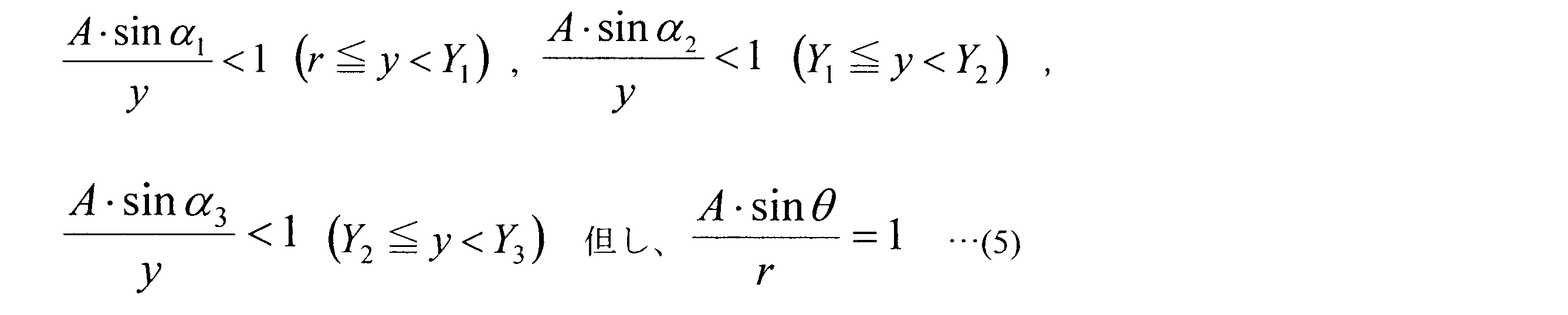
- ⁇ 1 ⁇ and ⁇ 2 and ⁇ 3 are determined so as to satisfy the following equation (5).
- FIG. 10 is a diagram showing the relationship between the displacement x in the tapered portion 21W on the horizontal axis and the value of the creeping direction stress Ex on the vertical axis.
- the model of FIG. 5 is indicated by a broken line
- the model of FIG. 9 is indicated by a solid line.
- the stress in the creeping direction at the tip of the first tapered portion 211 that is expected to cause the most deterioration in stress resistance is It can be seen that it is reduced by 30% or more compared to the conventional tapered portion 21X having a constant inclination angle ⁇ throughout. It can also be seen that the maximum value of the creeping stress in the entire tapered portion 21W can be reduced by 20%. Note that the length L in the cable longitudinal direction of the tapered portion 21W can be made shorter. In that case, each of X 1 , X 2 , and X 3 may be made smaller than the above value within a range satisfying the expression (5).
- FIG. 11 shows a diagram showing the correlation between the displacement x of the tapered portion 21 having the first and second equal-diameter portions 214 and 215 and the creeping direction stress Ex.
- the length in the cable longitudinal direction of each of the equal diameter portions 214 and 215 is set to 20 [mm] or more, more preferably 30 [mm] or more.
- the equal diameter portions 214 and 215 are lengthened, the entire taper-shaped portion 21 becomes longer. As a result, the entire intermediate connection portion is enlarged.
- 215 have a length of 100 [mm] or less, and more preferably 50 [mm] or less.
- each equal diameter portion is set to 30 [mm].
- the model in FIG. 9 is indicated by a two-dot chain line
- the characteristics of the tapered portion 21 are indicated by a solid line.
- the tapered portion 21 since the outer peripheral surfaces of the respective equal-diameter portions 214 and 215 are not inclined, the stress sharing in the creeping direction is not performed, and in the region of the respective equal-diameter portions 214 and 215, the creeping stress is generated.
- the value of Ex is 0.
- the entire length of the tapered portion 21 is increased by the length of each of the equal diameter portions 214 and 215.
- the value of the creeping direction stress of each taper part 211,212,213 is the same value as each taper part 211,212,213 of the taper-shaped part 21W.
- the tapered portion 21 of the first embodiment is composed of three tapered portions 211, 212, 213, but may be composed of more or fewer tapered portions, and is composed of two tapered portions. You may do it.
- the tapered portion 21 ⁇ / b> A includes a first tapered portion 211, a second tapered portion 212, and a first equal-diameter portion 214 is illustrated.
- the inclination angle alpha 1 of the first tapered portion 211 second and the inclination angle ⁇ of the inclination angle ⁇ of the conventional tapered portion consisting of a single tapered surface of the tapered portion 212, ⁇ 1 ⁇ 2 , ⁇ 1 ⁇ , ⁇ 2 > ⁇ .
- ⁇ 1 2.3
- ⁇ 2 4.2
- ( ⁇ 3.45 °).
- the tapered portion 21A The switching point between the first taper part 211 and the second taper part 212 (the first taper part 211 of the first taper part 211), with the tip end portion (minimum diameter portion) being the origin in the x direction and the cable center line C being the origin in the y direction.
- the maximum diameter portion) is (X 1 , Y 1 )
- the rear end portion (maximum diameter portion) of the second taper portion 212 is (X 2 , Y 2 ).
- the coordinate of the rear end portion of the second tapered portion 212 has a (X 2 + l1, Y 2 ).
- l1 is the length of the equal-diameter portion 214 in the x direction.
- the total length of the second tapered portion 212) was made equal to that in FIG. Note that if X 1 is smaller than 140, the length of the cable longitudinal direction is shortened, the longer the cable length in the longitudinal direction of greater than 140.
- FIG. 13 shows a diagram showing the relationship between the displacement x in the model not considering the equal diameter portion 214 of the tapered portion 21A on the horizontal axis and the value of the creeping direction stress Ex on the vertical axis. In FIG. 13, the model of FIG. 5 is indicated by a broken line.
- the stress in the creeping direction at the tip portion of the first taper portion 211 that is expected to cause the most deterioration in stress resistance is It can be seen that it is reduced by 30% or more compared to the conventional tapered portion 21X having a constant inclination angle ⁇ throughout. Further, the position where the maximum stress in the creeping direction moves to the boundary between the first taper portion 211 and the second taper portion 212, but since this position is away from the superconducting conductor layer 14, cooling is performed. Since the influence of shrinkage at the time is small and the insulation performance is hardly lowered, the occurrence of dielectric breakdown is avoided.
- FIG. 14 shows a diagram showing the relationship between the displacement x in the model considering the equal diameter portion 214 of the tapered portion 21A on the horizontal axis and the value of the creeping direction stress Ex on the vertical axis.
- the model of FIG. 5 is indicated by a broken line
- the model not considering the equal diameter portion 214 is indicated by a two-dot chain line.
- the length in the cable longitudinal direction of the equal-diameter portion 214 is 20 [mm] or more, more desirably 30 [mm] or more, and 100 [mm] or less, and more desirably 50 [mm] or less.
- the equal diameter portion 214 is set to 30 [mm].
- the model in FIG. 5 is indicated by a broken line
- the model in FIG. 13 is indicated by a two-dot chain line
- the characteristics of the tapered portion 21A are indicated by a solid line.
- the value of the creeping direction stress Ex is 0 in the region of the equal diameter portion 214.
- the entire length of the tapered portion 21 is increased by the length of the equal diameter portion 214.
- the values of the stress in the creeping direction of the respective taper portions 211 and 212 showed the same values as when the equal diameter portion 214 was not provided.
- the tapered portion 21B is composed of a plurality of (for example, n) first to n tapered portions 211B, 212B, 213B,.
- the example of this FIG. 15 has shown the case where the equal diameter part (step part) is not provided in the boundary of each taper part, you may provide an equal diameter part (step part).
- the values of X 2 to X n are added by the total length of each equal diameter portion (step portion).
- the first taper portion 211B located closest to the center has an X in the longitudinal direction of the cable of the first taper portion 211B when the tip (X 0 , Yr) of the tapered portion 21B is used as a base point.
- the inclination angle alpha 1 of the tapered portion satisfies the condition of the following expression (7).
- the coefficient A is defined by equation (11)
- the angle ⁇ in equation (11) is defined by equation (12).
- R is the radius of the outer circumference of the electrically insulating layer 20
- r is the radius of the outer circumference of the superconducting conductor layer 14
- R j is the radius of the outer periphery of the second reinforcing insulating layer 50
- theta is assumed sole taper tapered portion 21B It is the inclination angle obtained from the target withstand voltage V of the superconducting conductor layer 14, the breaking strength g x in the creeping direction of the taper surface, and the radius of each part when it is assumed that it is formed by the part.
- x is a variable indicating a position on the x-axis (cable center line C direction)
- y is a variable indicating a position on the y-axis (cable radial direction).
- the tip position of the taper portion 211B that is the boundary between the superconducting conductor layer 14 and the first first taper portion 211B is (X 0 , Yr), and thereafter the maximum diameter portion of each taper portion up to the nth is defined. Let (X n , Y n ).
- the second taper portion 212B located second inward is in the range of (X 1 , Y 1 ) to (X 2 , Y 2 ), and the inclination angle ⁇ 2 of the taper portion 212B is expressed by the following equation.
- the condition of (8) is satisfied. That is, the inclination angle alpha 2 as the left expression of the left side is always less than 1 in the formula (8) is set in the above range.
- the third tapered portion 213B located inside the third is, in the above, (X 2, Y 2) ⁇ (X 3, Y 3) in a range of inclination angle alpha 3 is the formula of the tapered portion 213B ( The condition of 9) is satisfied.
- an inclination angle alpha 3 as the left expression of the left side is always less than 1 in the formula (9) is set in the above range.
- the number of taper portions in the taper-shaped portion 21B is preferably two or three, but may be a larger number (for example, n), in which case, the taper portion located on the nth inner side. 21 nB ranges from (X n ⁇ 1 , Y n ⁇ 1 ) to (X n , Y n ), and the inclination angle ⁇ n of the tapered portion 21 nB satisfies the condition of the general formula (10).
- the inclination angle ⁇ n is set so that the left side of the left expression of Expression (10) is always less than 1 in the above range.
- the taper-shaped portion 21B is formed from a plurality of taper portions, and as shown in FIG. 16, the displacement x in the x-axis direction in the taper-shaped portion 21B is taken on the horizontal axis, and the value of the laminar stress Ex is set to the vertical direction.
- a diagram showing these relationships as axes is shown in FIG.
- the stress in the laminating direction for each tapered portion 211B, 212B, 213B when the inclination angle in each tapered portion is set so as to satisfy the expressions (7) to (12), the stress in the laminating direction for each tapered portion 211B, 212B, 213B,.
- the position with the smallest diameter is the maximum value. That is, the boundary position with the other tapered portion adjacent on the small diameter side is the highest value.
- the stress in the layering direction at the tip of the first tapered portion 211B which is the innermost is the lowest value, and they control the angles ⁇ 1 , ⁇ 2 , ⁇ 3 .
- the respective boundary positions (X 0 , Yr), (X 1 , Y 1 ), (X 2 , Y 2 ) the following conditions are required to be satisfied.
- the stress in the creeping direction at the boundary positions (X 0 , Yr), (X 1 , Y 1 ), (X 2 , Y 2 ) is also a low value according to the order in which the tapered portions 211B, 212B, and 213B are inside. More desirable. That is, in this case, the following conditions are satisfied at each of the boundary points (X 0 , Yr), (X 1 , Y 1 ), (X 2 , Y 2 ).
- the tapered portion 21 is formed in each of the electrical insulating layers 20 on both sides of the conductor connection portion S.
- the taper-shaped portion 21 has an inclination angle that increases stepwise as the distance from the conductor connection portion increases, the overall length of the taper-shaped portion 21 does not increase and can be shortened, and the intermediate connection portion can be reduced in size and It is possible to reduce the forming work load and the work time.
- the taper-shaped part 21 has the equal diameter part 214 or 215, it has high adhesiveness by further winding an insulating paper around the outer periphery, and the boundary between the taper-shaped part 21 and the first reinforcing insulating layer 30 Therefore, it is possible to provide a connection structure with excellent insulation performance.
- each taper part 211, 212, 213 when the grading is performed using an insulating paper having a smaller thickness as the inner layer is formed, the construction of each taper part 211, 212, 213 is facilitated. Furthermore, insulation performance is also improved. This is because the stepping width can be made constant while keeping the slope angle constant, and the adhesiveness with the insulating paper for filling the valley is improved.
Abstract
Description
超電導ケーブルは、断熱管内にケーブルコアを収納した構造であり、ケーブルコアは、中心からフォーマ、超電導導体層、電気絶縁層等が積層されて構成されている。
また、断熱管は、内管と外管からなる二重管構造を採っており、内管と外管の間は真空引きされ、内管の内部には液体窒素などの冷媒が循環されて、極低温状態で送電が行われる。
この中間接続部では、ケーブルコアの接続に、その絶縁構造が類似する油浸絶縁ケーブル(OF[oil-filled]ケーブル)の接続技術を応用している。即ち、図17に示すように、接続を行う超電導ケーブルのそれぞれについて、超電導導体101の外側で電気絶縁部を形成する絶縁紙をペンシリング状(鉛筆形状)にむき出してテーパ形状に形成する。
そして、超電導導体同士を接続した後に、互いに対向するペンシリング状に剥き出された一方の電気絶縁部102のテーパ形状部と他方の電気絶縁部102のテーパ形状部の間に新たな絶縁紙の巻回により新たに電気絶縁部103を形成し、さらに、その周辺を既存の絶縁部102よりも大径となるように絶縁紙を巻いて、絶縁部を補強した補強絶縁部104を形成して、中間接続部の絶縁を図っている(例えば、非特許文献1参照)。
一方、超電導ケーブルの場合には、ケーブルコアの周囲に冷媒が供給されることから、互いに対向する電気絶縁部のテーパ形状部同士の間の谷埋めには、乾いた絶縁紙が使用される。乾いた絶縁紙は絞りながら巻き付けようとすると千切れやすいため、比較的、緩く巻き付けが行われる。
そのため、テーパ形状部において、元々の絶縁部と新たに谷埋めのために形成された絶縁部との密着性が弱くなり、テーパ形状部のテーパ面に沿った沿層方向の耐電位傾度(耐電界ストレス)が低くなるという問題が生じていた。
また、この耐電界ストレスは超電導導体に近い内側ほど大きくなるが、電気絶縁部の内側は導体が外気温から-200℃まで冷やされる事により、長手方向だけでなく径方向にも縮むため、電気絶縁部の内側ほど密着性が弱く、隙間も生じやすくなるので、さらに、中間接続部の電気性能を下げてしまうことが問題となっていた。
また、本発明は、前記補強絶縁層が内側から順に積層された複数層から構成され、当該複数層は各々の前記段部に外径が等しくなるまで絶縁性紙類を巻回して形成されており、前記順に積層された複数層の各々は、その内側の層と当該内側の層と外径が等しい前記段部との境界を覆うように前記絶縁紙類が巻回されて形成されるようにしても良い。
また、前記段部のケーブル長手方向における長さが20[mm]以上100[mm]以下としても良い。

但し、Rは電気絶縁層の外周の半径、rは超電導導体層の外周の半径、Rjは補強絶縁層の外周の半径、θはテーパ形状部を仮想的に単独のテーパ部で形成したものと仮定した場合において、超電導導体層の目標耐電圧V、テーパ面の沿層方向の破壊強度gx及び前記R、Rj、rの値から求めた傾斜角度、xはテーパ形状部の先端部を原点としてケーブル長手方向に沿った線上での位置を示す変数、yはケーブル中心線を原点として半径方向外側に向かう線上での位置を示す変数、X1~nとY1~nはx-y座標平面における前記一番目からn番目までのテーパ部の最大径部の位置座標である。
また、本発明は、前記複数のそれぞれのテーパ部における沿層方向ストレスの最大値は、最も外側のテーパ部で生じる構成としても良い。
さらに、本発明は、前記複数のそれぞれのテーパ部の先端部における沿層方向ストレスの値は、内側のテーパ部ほど低くなる構成としても良い。
電気絶縁層は、内側の超電導導体層に近いほど電界ストレスが大きくなり、その一方で、電気絶縁層は、その内側の超電導導体層が冷媒の冷却によって収縮するため、テーパ形状部の先端部では、テーパ面の沿層方向に沿って絶縁性能の低下が生じやすくなる。
しかしながら、本発明では、各テーパ形状部の先端側(径の小さい方)の傾斜角度を後端側(径の大きい方)よりも小さく形成しているので、電界ストレスの沿層方向成分を低減することができ、沿層方向における絶縁破壊の発生を低減することが可能となる。
また、テーパ形状部は導体接続部から離れるほど段階的に傾斜角度が大きくなるので、テーパ形状部全体の傾斜角度を小さくする場合に比べてテーパ形状部の全長を短縮することができ、接続構造の小型化を図ると共にその形成作業負担や作業時間を低減することが可能となる。
以下、本発明の第一の実施の形態を図面に基づいて詳細に説明する。
図1は布設される超電導ケーブルの一例を示す図、図2は超電導ケーブルの中間接続部におけるケーブルコアの主要な接続構造を示す断面図である。
図1に示す超電導ケーブル10は、断熱管12内に一心のケーブルコア11が収納された単心型の超電導ケーブルである。ケーブルコア11は、フォーマ13、超電導導体層14、電気絶縁層20、超電導シールド層15、常電導シールド層16、保護層17等により構成される。
超電導導体層14を構成する超電導線材は、例えば、テープ状の金属基板上に中間層、超電導層、保護層等が順に形成された積層構造を有している。超電導層を構成する超電導体には、液体窒素温度以上で超電導を示すRE系超電導体(RE:希土類元素)、例えば化学式YBa2Cu3O7-yで表されるイットリウム系超電導体(以下、Y系超電導体)が代表的である。また、金属マトリクス中に超電導体が形成されているテープ状の超電導線材でもよい。この超電導体には、ビスマス系超電導体、例えば化学式Bi2Sr2CaCu2O8+δ(Bi2212), Bi2Sr2Ca2Cu3O10+δ(Bi2223)を適用できる。
なお、化学式中のδは酸素不定比量を示す。
保護層17は、例えば絶縁紙、高分子不織布などで構成され、常電導シールド層16の外周に巻回することにより形成される。
断熱内管121及び断熱外管122は、例えばステンレス製のコルゲート管(波付き管)である。断熱内管121と断熱外管122の間には、例えばアルミを蒸着したポリエチレンフィルムの積層体で構成された多層断熱層(スーパーインシュレーション)123が介在し、真空状態に保持される。また、断熱外管122の外周はポリ塩化ビニル(PVC)やポリエチレンなどの防食層124で被覆されている。
超電導ケーブル10同士の接続の際には、互いの断熱管12同士を連結する図示しない固定ボックスが使用される。この固定ボックスは、断熱管12と同様に二重壁面構造であり、壁面間が真空引きされると共にボックス内部には冷媒が循環される。また、ボックス内部において、各超電導ケーブル10のケーブルコア11同士が連結される。
そして、二つの超電導導体層14の接続端部の上面(外周面)において、各超電導導体層14の超電導層同士が導通するように半田を介在させて接続用超電導線材(図示略)を架設状態で貼着し、各超電導導体層14の電気的な接続が行われる。なお、超電導導体層14の超電導層を構成する超電導線材同士を直接1本ずつ半田により接続することも可能である。
次に、電気絶縁層20について図2及び図3により説明する。図3はフォーマ13及び超電導導体層14が接続され、後述する第一と第二の補強絶縁層30,50が未形成の状態を示す断面図である。図2及び3において、符号Sはフォーマ13及び超電導導体層14の導体接続部を示している。
図3に示すように、各ケーブルコア11の電気絶縁層20は、いずれも、導体接続部Sに向かうにつれて段階的に縮径するテーパ形状部21を有している。このテーパ形状部21は、三段階で縮径しており、導体接続部Sの外周には電気絶縁層20は形成されていない。即ち、テーパ形状部21は、段階的に傾斜角度が変化する複数のテーパ部として、外径が最も小さい(最も導体接続部Sに近い)第一のテーパ部211と、その次に外径が小さい(その次に導体接続部Sに近い)第二のテーパ部212と、最も外径が大きい(最も導体接続部Sから遠い)第三のテーパ部213とを備えている。また、第一のテーパ部211と第二のテーパ部212の間には、外径が一定である段部としての第一の等径部214が形成され、第二のテーパ部212と第三のテーパ部213の間には、外径が一定である段部としての第二の等径部215が形成されている。
そして、第一のテーパ部211と第二のテーパ部212と第三のテーパ部213の各々のテーパ面におけるケーブルの中心線Cに対する傾斜角度α1,α2,α3の大小関係は、α1<α2<α3となっている。
また、互いに対向するテーパ形状部21,21の間の谷部分には、図2に示すように、当該谷部分を埋めるように第一の補強絶縁層30が形成されており、第一の補強絶縁層30の外周には、当該第一の補強絶縁層30及び各テーパ形状部21,21を含む電気絶縁層20,20の端部を被覆するように第二の補強絶縁層50が形成されている。
即ち、第一の補強絶縁層30の最も内側の層は、超電導導体層14の外径から第一の等径部214の外径までの範囲内に形成された三つの分割層31,32,33から構成されている。
上記分割層31は、超電導導体層14の外周面上に、外径が第一の等径部214と等しくなるまでスロープ紙を巻き付けることで形成される。スロープ紙とは、幅広の絶縁紙であって、その両側端部が予め紙の長手方向において斜めに切断されており、巻き付けると、両端にテーパ形状を形成することが出来、その断面が略等脚台形状に形成される。この分割層31は、少なくとも導体接続部Sを単独で被覆することが可能な幅で形成される。
また、分割層32,33は、分割層31の両端部とそれぞれの第一のテーパ部211,211との隙間領域を埋めるように、電気絶縁層20の絶縁紙よりも幅の狭い帯状の絶縁紙を巻き付けることにより形成される。
なお、スロープ紙の幅は200~500mm程度、電気絶縁層20の絶縁紙の幅は20~30mm程度、分割層31の絶縁紙の幅は8~12mm程度とすればよい。
そして、分割層31の中心線C方向の幅(台形断面の上辺と下辺の平均幅)は分割層32,33よりも広くなっており、分割層31が幅の広い絶縁層として機能し、分割層32,33が幅の狭い絶縁層として機能する。
上記分割層34は、一方の第一の等径部214の外周面から分割層31の外周面までを跨いでこれらの上から、外径が第二の等径部215と等しくなるまでスロープ紙を巻き付けることで形成される。これにより、分割層34は、分割層31と分割層32の境界及び分割層32と第一の等径部214との境界を完全に被覆した状態となっている。
また、上記分割層35は、他方の第一の等径部214の外周面から分割層31の外周面までを跨いでこれらの上から、外径が第二の等径部215と等しくなるまでスロープ紙を巻き付けることで形成される。これにより、分割層35は、分割層31と分割層33の境界及び分割層33と第一の等径部214との境界を完全に被覆した状態となっている。
また、分割層36,37,38は、それぞれ、一方の第二のテーパ部212と分割層34との隙間領域、分割層34と分割層35との隙間領域、分割層35と他方の第二のテーパ部212との隙間領域を埋めるように、幅の狭い帯状の絶縁紙の巻回により形成される。
そして、分割層34,35の中心線C方向の幅(台形断面の上辺と下辺の平均幅)は分割層36,37,38よりも広くなっており、分割層34,35が幅の広い絶縁層として機能し、分割層36,37,38が幅の狭い絶縁層として機能する。
上記分割層39は、一方の第二の等径部215の外周面から分割層34の外周面までを跨いでこれらの上から、外径が電気絶縁層20と等しくなるまでスロープ紙を巻き付けることで形成される。これにより、分割層39は、分割層34と分割層36の境界及び分割層36と第二の等径部215との境界を完全に被覆した状態となっている。
また、上記分割層40は、分割層34の外周面から分割層35の外周面までを跨いでこれらの上から、外径が電気絶縁層20と等しくなるまでスロープ紙を巻き付けることで形成される。これにより、分割層40は、分割層34と分割層37の境界及び分割層37と分割層35との境界を完全に被覆した状態となっている。
また、上記分割層41は、分割層35の外周面から他方の第二の等径部215の外周面までを跨いでこれらの上から、外径が電気絶縁層20と等しくなるまでスロープ紙を巻き付けることで形成される。これにより、分割層41は、分割層35と分割層38の境界及び分割層38と第二の等径部215との境界を完全に被覆した状態となっている。
また、分割層42,43,44,45は、それぞれ、一方の第三のテーパ部213と分割層39との隙間領域、分割層39と分割層40との隙間領域、分割層40と分割層41との隙間領域、分割層41と他方の第三のテーパ部213との隙間領域を埋めるように、幅の狭い帯状の絶縁紙の巻回により形成される。
そして、分割層39~41の中心線C方向の幅(台形断面の上辺と下辺の平均幅)は分割層42~45よりも広くなっており、分割層39~41が幅の広い絶縁層として機能し、分割層42~45が幅の狭い絶縁層として機能する。
テーパ形状部21についてより詳細に説明する。
まず、「テーパ部の傾斜角度」について定義する。
図4に示すように、テーパ部211(第一のテーパ部211を図示するが第二、第三のテーパ部212,213も同様である)の中心線方向の長さをL211とし、第一のテーパ部211の最大外径部における絶縁紙の層の厚みをtとすると、テーパ部211の傾斜角度θ0は次式(1)により定義される。

また、全点が直線上に並ばない場合には、例えば、最下部の頂点t1と最上部の頂点t5とを結ぶ直線を基線Fとしても良いし、頂点t1~tnから最小二乗法で基線Fを求めても良い。
そして、目標耐電圧をV、テーパ形状部21Xのテーパ面の沿層方向(テーパ面の傾斜角度に沿った方向)の破壊強度をgxとした場合の変位xと各パラメータとの間には次式(2)が成立する。さらに、上式(2)において変位y=Rとした場合、次式(3)が成立する。

さらに、上記パラメータと式(1)~(3)により沿層方向ストレスExは次式(4)で与えられる。なお、図5における沿層方向ストレスExがテーパ形状部21Xの先端部(x=0)において1となるように規格化して、沿層方向ストレスExとxの相関を説明する。つまり、次式(4)において、係数Aはx=0の時に、y=rであり、Ex=1となるように定めた。従って、A・sinθ/r=1である。

一方、超電導ケーブル10では、断熱管12内を循環する冷媒により、ケーブルコア11を冷却することが必須であるため、冷却により、フォーマ13及び超電導導体層14が半径方向に大きく熱収縮を生じることから、絶縁紙を積層する構造のテーパ形状部21の先端部には超電導導体層14との開きが生じて、計算通りの絶縁強度を安定して得る事が実際上は困難である。
さらに、最も内側の第一のテーパ部211の傾斜角度α1についてはα1<θとなるように設定している。
ここで、式(4)のθをα1~α3に置き換えると、第一のテーパ部211における沿層方向ストレスExが求められるが、これによれば、α1~α3が小さいほど、沿層方向ストレスExを小さくすることができる。
第一のテーパ部211(212,213も同様)を形成するためには、図7に示すように、絶縁紙の巻き付け端部の位置を一層毎に一定のステッピング幅Pでずらして、第一のテーパ部211全体が目的の傾斜角度α1となるように調整する。即ち、絶縁紙の厚さをdとすると、第一のテーパ部211の傾斜角度α1とステッピング幅Pと絶縁紙の厚さdとの間には、tanα1=d/Pが成立するように、ステッピング幅Pと絶縁紙の厚さdとを選択する。
このように電気絶縁層20が形成されている場合には、前述したステッピング幅Pをギャップ幅Gより大きくすると、テーパ部211において内側の絶縁紙の押さえが効かなくなるので、絶縁紙のステッピング幅Pはギャップ幅G以下とすることが望ましい。
例えば、絶縁紙のギャップ幅G=3[mm]であって、第一~第三のテーパ部211,212,213の全てについて、ステッピング幅Pをその取り得る最大値である3[mm]とした場合、各テーパ部211,212,213の傾斜角度は絶縁紙の厚さdを変えて調整する。各テーパ部211,212,213についてそれぞれ絶縁紙の厚さdを120,170,220[μm]とすると、傾斜角度α1=2.3°、α2=3.3°、α3=4.2°となる。
θは、要求される破壊強度gxと、超電導ケーブルの各部のサイズ、例えば、規格サイズにより一義的に求められるものであり、要求される破壊強度gxや、超電導ケーブルのサイズにより変動する。
傾斜角度α1=2.3°,α2=3.3°,α3=4.2°(θ=3.45°)とする。さらに、ケーブル中心線Cに沿った方向をx、ケーブル中心線Cを中心とするケーブルの半径方向をyとするx-y座標系において、テーパ形状部21Wの先端部(最小径部)をx方向の原点、ケーブル中心線Cをy方向の原点として、第一のテーパ部211と第二のテーパ部212との切換点(第一のテーパ部211の最大径部)を(X1、Y1)、第二のテーパ部212と第三のテーパ部213との切換点(第二のテーパ部212の最大径部)を(X2、Y2)、第三のテーパ部213の後端部(最大径部)を(X3、Y3)とする。
この場合、α1<θであって、α2,α3は次式(5)を具備するように決定されている。
テーパ形状部21Wにおける変位xを横軸にとり、沿層方向ストレスExの値を縦軸としたこれらの関係を示す線図を図10に示す。この図10において、図5のモデルを破線で示し、図9のモデルを実線で示す。
このように、テーパ形状部21Wにおいて、傾斜角度を三段階で変化させた結果、最もストレスの耐性の低下を生じることが予想される第一のテーパ部211の先端部における沿層方向ストレスは、全体を通じて一定の傾斜角度θとする従来のテーパ形状部21Xと比べて30%以上低減させることが分かる。また、テーパ形状部21Wにおける全体の中での沿層方向ストレスの最大値も20%削減できることが分かる。
なお、テーパ形状部21Wにおけるケーブル長手方向の長さLはより短くすることも可能である。その場合、式(5)を満足する範囲で、X1、X2、X3のそれぞれを上記の値より小さくしてやればよい。
この場合、各等径部214、215のケーブル長手方向の長さを20[mm]以上、より望ましくは30[mm]以上とする。しかし、各等径部214,215を長くすると、テーパ形状部21の全体が長くなり、結果として、中間接続部全体が大型化するので、大きさに制限がある場合は、各等径部214,215の長さは100[mm]以下、より望ましくは、50[mm]以下とする。
図11の例では、各等径部をいずれも30[mm]とした。なお、比較のため、図5のモデルを破線で示し、図9のモデルを二点鎖線で示し、テーパ形状部21の特性を実線で示した。
テーパ形状部21の場合、それぞれの等径部214,215はその外周面が傾斜していないので、沿層方向のストレス分担を行わず、各等径部214,215の領域では沿層方向ストレスExの値は0となる。また、各等径部214,215の長さ分だけ、テーパ形状部21の全長が長くなる。また、各テーパ部211,212,213の沿層方向ストレスの値は、テーパ形状部21Wの各テーパ部211,212,213と同じ値を示す。
第一の実施形態のテーパ形状部21は、三つのテーパ部211,212,213から構成されているが、より多くのテーパ部から構成しても良いし、より少なく、二つのテーパ部から構成しても良い。この第二の実施形態では、図12に示すように、テーパ形状部21Aが、第一のテーパ部211と第二のテーパ部212と第一の等径部214とを備える場合について例示する。この場合も、第一のテーパ部211の傾斜角度α1と第二のテーパ部212の傾斜角度βと単一のテーパ面からなる従来のテーパ形状部における傾斜角度θとは、α1<α2、α1<θ、α2>θとなっている。具体的にはα1=2.3、α2=4.2、(θ=3.45°)とした。
さらに、等径部214を考慮しない場合において、ケーブル中心線Cに沿った方向をx、ケーブル中心線Cを中心とするケーブルの半径方向をyとするx-y座標系において、テーパ形状部21Aの先端部(最小径部)をx方向の原点、ケーブル中心線Cをy方向の原点として、第一のテーパ部211と第二のテーパ部212との切換点(第一のテーパ部211の最大径部)を(X1、Y1)、第二のテーパ部212の後端部(最大径部)を(X2、Y2)とする。
なお、図12は等径部214を備える場合を例示しているので、第二のテーパ部212の後端部の座標は(X2+l1、Y2)となっている。l1は等径部214のx方向の長さである。
X1,α2は次式(6)を具備するように決定される。例えば、r=17.7としているので、X1>96とすればよい。

ここで、テーパ形状部21Aの等径部214を考慮しないモデルにおける変位xを横軸にとり、沿層方向ストレスExの値を縦軸としたこれらの関係を示す線図を図13に示す。この図13において、図5のモデルを破線で示す。
また、沿層方向ストレスの最大値となる位置が、第一のテーパ部211と第二のテーパ部212との境界に移動するが、この位置は、超電導導体層14から離れているので、冷却時の収縮の影響が小さく、絶縁性能の低下が生じにくいので、絶縁破壊の発生は回避される。
この場合も、等径部214のケーブル長手方向の長さを20[mm]以上、より望ましくは30[mm]以上であって、100[mm]以下、より望ましくは、50[mm]以下とする。
図14の例では、等径部214を30[mm]とした。なお、比較のため、図5のモデルを破線で示し、図13のモデルを二点鎖線で示し、テーパ形状部21Aの特性を実線で示した。
テーパ形状部21Aの場合も、等径部214の領域では沿層方向ストレスExの値は0となる。また、等径部214の長さ分だけ、テーパ形状部21の全長が長くなる。また、各テーパ部211,212の沿層方向ストレスの値は、等径部214を設けない場合と同じ値を示した。
この第三の実施形態では、テーパ形状部21Bが、図15に示すように、複数(例えばn個)の段階的な第一~nのテーパ部211B,212B,213B,…から構成され、一番目からn番目の各テーパ部211B,212B,213B,…の傾斜角度α1~αnが次の条件式(7)~(12)を満たすようにしたことを特徴とする。
なお、この図15の例では、各テーパ部の境界における等径部(段部)を設けていない場合を示しているが、等径部(段部)を設けても良い。なお、等径部(段部)を設けた場合には、X2~Xnの値が各等径部(段部)の長さの合計分だけ加算される。

即ち、Rは電気絶縁層20の外周の半径、rは超電導導体層14の外周の半径、Rjは第二の補強絶縁層50の外周の半径、θはテーパ形状部21Bを仮に単独のテーパ部で形成したものと仮定した場合において超電導導体層14の目標耐電圧V、テーパ面の沿層方向の破壊強度gx及び各部の半径から求めた傾斜角度である。
また、xはx軸(ケーブルの中心線C方向)上での位置を示す変数、yはy軸(ケーブルの半径方向)上での位置を示す変数である。また、超電導導体層14と一つ目の第一のテーパ部211Bの境界であるテーパ部211Bの先端位置を(X0,Yr)、それ以降、n番目までの各テーパ部の最大径部を(Xn,Yn)とする。
その場合、基点(X0,Yr)であるテーパ形状部21Bの先端部から(X1,Y1)までの範囲において式(7)の左式の左辺が常に1未満となるようにその傾斜角度α1が設定されている。
つまり、上記範囲において式(8)の左式の左辺が常に1未満となるようにその傾斜角度α2が設定されている。
三番目に内側に位置する第三のテーパ部213Bは、上において、(X2,Y2)~(X3,Y3)の範囲で、そのテーパ部213Bの傾斜角度α3が次式(9)の条件を満たしている。
つまり、上記範囲において式(9)の左式の左辺が常に1未満となるようにその傾斜角度α3が設定されている。
このように、テーパ形状部21Bにおいてテーパ部の数は二又は三とすることが望ましいが、それ以上の数(例えばn)であってもよく、その場合、n番目に内側に位置するテーパ部21nBは、(Xn-1,Yn-1)~(Xn,Yn)までの範囲で、そのテーパ部21nBの傾斜角度αnが一般式(10)の条件を満たしている。また、上記範囲において式(10)の左式の左辺が常に1未満となるようにその傾斜角度αnが設定されている。
テーパ形状部21Bにおいて、各テーパ部における傾斜角度を式(7)~(12)を満たすように設定した場合、各テーパ部211B,212B,213B,…ごとの延層方向ストレスは、各テーパ部内で最も小径となる位置が最大値となる。即ち、小径側で隣接する他のテーパ部との境界位置が最も高い値となる。
つまり、各境界位置(X0,Yr)、(X1,Y1)、(X2,Y2)の例では以下の条件が成立することが求められる。
A・sinα1/Yr<A・sinα2/Y1 且つ A・sinα1/Yr<A・sinα3/Y2
従って、最もストレスの耐性の低下を生じることが予想される第一のテーパ部211Bの先端部における沿層方向ストレスを十分に低減させることが分かる。
なお、上記のA・sinα2/Y1とA・sinα3/Y2とはいずれが大きくともよい。但し、各テーパ部211B,212B,213Bが内側となる順番に従って各境界位置(X0,Yr)、(X1,Y1)、(X2,Y2)における沿層方向ストレスも低い値となることがより望ましい。
つまり、その場合、各境界点(X0,Yr)、(X1,Y1)、(X2,Y2)では以下の条件が成立する。
A・sinα1/Yr<A・sinα2/Y1<A・sinα3/Y2
上記超電導ケーブル10の中間接続部では、導体接続部Sの両側の電気絶縁層20の各々にテーパ形状部21を形成し、テーパ形状部21は導体接続部Sに近いものほどテーパ部の傾斜角度が小さくなるように複数のテーパ部から形成されている。
このため、超電導導体層14の冷却による収縮で、絶縁性紙類のゆるみが生じ易いテーパ形状部21の先端部であっても、電界ストレスの沿層方向成分を低減することができ、沿層方向における絶縁破壊の発生を低減することが可能となる。
また、導体接続部から離れるほどテーパ形状部21は段階的に傾斜角度が大きくなるので、テーパ形状部21の全長が長くならず、短縮することができ、中間接続部の小型化を図ると共にその形成作業負担や作業時間を低減することが可能となる。
12 断熱管
13,13X フォーマ
14,14X 超電導導体層
20,20X 電気絶縁層
21,21A,21W,21X テーパ形状部
30 第一の補強絶縁層
31,34,35,39,40,41 分割層(幅の広い絶縁層)
32,33、36,37,38,42,43,44,45 分割層(幅の狭い絶縁層)
50,50X 第二の補強絶縁層
211 第一のテーパ部(テーパ部)
212 第二のテーパ部(テーパ部)
213 第三のテーパ部(テーパ部)
214 第一の等径部(段部)
215 第二の等径部(段部)
Ex 沿層方向ストレス
S 導体接続部
α1,α2,α3 傾斜角度
θ 傾斜角度
Claims (9)
- フォーマと超電導導体層を有するケーブルコアが、断熱管内で冷媒と共に収容されてなる超電導ケーブル同士が接続された超電導ケーブルの接続構造であって、
前記ケーブルコアは、前記超電導導体層の周囲に絶縁性紙類を巻回した電気絶縁層を備え、
前記フォーマと前記超電導導体層とを接続してなる導体接続部の両側の前記電気絶縁層は、いずれも前記導体接続部に向かうにつれて縮径するテーパ形状部を有し、
当該テーパ形状部は、前記導体接続部に近いものほど傾斜角度が小さい複数のテーパ部により段階的に傾斜角度が変化して形成されており、
前記各テーパ形状部の間に補強絶縁層を備えることを特徴とする超電導ケーブルの接続構造。 - 前記各テーパ形状部は、段階的に傾斜角度が変化する複数のテーパ部の境界位置に外径が一定となる段部を有することを特徴とする請求項1記載の超電導ケーブルの接続構造。
- 前記補強絶縁層は内側から順に積層された複数層から構成され、当該複数層は各々の前記段部に外径が等しくなるまで絶縁性紙類を巻回して形成されており、
前記順に積層された複数層の各々は、その内側の層と当該内側の層と外径が等しい前記段部との境界を覆うように前記絶縁紙類が巻回されて形成されていることを特徴とする請求項2記載の超電導ケーブルの接続構造。 - 前記補強絶縁層が内側から順に積層された複数層から構成され、当該複数層の各々が前記超電導ケーブルの長手方向において幅の広い絶縁層と、当該幅の広い絶縁層の両側に生じる隙間を埋める幅の狭い絶縁層とから構成され、
前記幅の広い絶縁層は、その内側の前記幅の狭い絶縁層の外周全体を被覆するように形成されていることを特徴とする請求項2又は3記載の超電導ケーブルの接続構造。 - 前記段部のケーブル長手方向における長さが20[mm]以上100[mm]以下であることを特徴とする請求項2から4のいずれか一項に記載の超電導ケーブルの接続構造。
- 前記テーパ形状部は、前記導体接続部に最も近いテーパ部を一番目とした場合に、当該一番目からn番目までのテーパ部の傾斜角度α1からαnが次式の条件を満たすことを特徴とする請求項1から5のいずれか一項に記載の超電導ケーブルの接続構造。

但し、Rは電気絶縁層の外周の半径、rは超電導導体層の外周の半径、Rjは補強絶縁層の外周の半径、θはテーパ形状部を仮想的に単独のテーパ部で形成したものと仮定した場合において、超電導導体層の目標耐電圧V、テーパ面の沿層方向の破壊強度gx及び前記R、Rj、rの値から求めた傾斜角度、xはテーパ形状部の先端部を原点としてケーブル長手方向に沿った線上での位置を示す変数、yはケーブル中心線を原点として半径方向外側に向かう線上での位置を示す変数、X1~nとY1~nはx-y座標平面における前記一番目からn番目までのテーパ部の最大径部の位置座標である。 - 前記テーパ部の数nが2又は3であることを特徴とする請求項6記載の超電導ケーブルの接続構造。
- 前記複数のそれぞれのテーパ部における沿層方向ストレスの最大値は、最も外側のテーパ部で生じることを特徴とする請求項6又は7記載の超電導ケーブルの接続構造。
- 前記複数のそれぞれのテーパ部の先端部における沿層方向ストレスの値は、内側のテーパ部ほど低くなることを特徴とする請求項8記載の超電導ケーブルの接続構造。
Priority Applications (4)
| Application Number | Priority Date | Filing Date | Title |
|---|---|---|---|
| EP13778306.4A EP2728689B1 (en) | 2012-04-19 | 2013-04-15 | Connection structure for superconducting cables |
| CN201380002185.3A CN103688433B (zh) | 2012-04-19 | 2013-04-15 | 超导电缆的连接结构 |
| JP2013548517A JP6155195B2 (ja) | 2012-04-19 | 2013-04-15 | 超電導ケーブルの接続構造 |
| US14/236,605 US9123455B2 (en) | 2012-04-19 | 2013-04-15 | Connection structure for superconducting cables |
Applications Claiming Priority (2)
| Application Number | Priority Date | Filing Date | Title |
|---|---|---|---|
| JP2012095482 | 2012-04-19 | ||
| JP2012-095482 | 2012-04-19 |
Publications (1)
| Publication Number | Publication Date |
|---|---|
| WO2013157513A1 true WO2013157513A1 (ja) | 2013-10-24 |
Family
ID=49383469
Family Applications (1)
| Application Number | Title | Priority Date | Filing Date |
|---|---|---|---|
| PCT/JP2013/061162 WO2013157513A1 (ja) | 2012-04-19 | 2013-04-15 | 超電導ケーブルの接続構造 |
Country Status (5)
| Country | Link |
|---|---|
| US (1) | US9123455B2 (ja) |
| EP (1) | EP2728689B1 (ja) |
| JP (1) | JP6155195B2 (ja) |
| CN (1) | CN103688433B (ja) |
| WO (1) | WO2013157513A1 (ja) |
Cited By (13)
| Publication number | Priority date | Publication date | Assignee | Title |
|---|---|---|---|---|
| KR20160084920A (ko) | 2015-01-06 | 2016-07-15 | 엘에스전선 주식회사 | 중간접속함 |
| KR101810357B1 (ko) * | 2017-03-30 | 2017-12-19 | 엘에스전선 주식회사 | 전력 케이블용 중간접속함을 이용한 직류 전력케이블 중간접속 시스템 및 직류 전력케이블 접속 방법 |
| KR101810359B1 (ko) * | 2017-03-31 | 2017-12-19 | 엘에스전선 주식회사 | 직류 전력케이블 중간접속 시스템 |
| KR101810360B1 (ko) * | 2017-03-31 | 2018-01-25 | 엘에스전선 주식회사 | 직류 전력케이블 중간접속 시스템 |
| KR101830033B1 (ko) * | 2017-03-31 | 2018-02-19 | 엘에스전선 주식회사 | 직류 전력케이블 중간접속 시스템 |
| KR101830030B1 (ko) * | 2017-03-31 | 2018-02-19 | 엘에스전선 주식회사 | 직류 전력케이블 중간접속 시스템 및 직류 전력케이블용 중간접속함 |
| KR101830032B1 (ko) * | 2017-03-31 | 2018-02-19 | 엘에스전선 주식회사 | 직류 전력케이블 중간접속 시스템 및 직류 전력케이블용 중간접속함 |
| KR101839725B1 (ko) * | 2017-03-30 | 2018-03-16 | 엘에스전선 주식회사 | 직류 전력케이블 중간접속 시스템 |
| KR20180111459A (ko) * | 2017-11-07 | 2018-10-11 | 엘에스전선 주식회사 | 전력 케이블용 중간접속함을 이용한 직류 전력케이블 중간접속 시스템 및 직류 전력케이블 접속 방법 |
| KR20180111458A (ko) * | 2017-11-07 | 2018-10-11 | 엘에스전선 주식회사 | 직류 전력케이블 중간접속 시스템 |
| KR20180111457A (ko) * | 2017-11-07 | 2018-10-11 | 엘에스전선 주식회사 | 직류 전력케이블 중간접속 시스템 |
| KR20180130161A (ko) * | 2017-05-29 | 2018-12-07 | 엘에스전선 주식회사 | 초고압 직류 전력케이블용 중간접속함 및 이를 포함하는 초고압 직류 전력케이블 접속시스템 |
| KR20180131053A (ko) * | 2017-05-31 | 2018-12-10 | 엘에스전선 주식회사 | 초고압 직류 전력케이블용 종단접속함 |
Families Citing this family (5)
| Publication number | Priority date | Publication date | Assignee | Title |
|---|---|---|---|---|
| CN104578184A (zh) * | 2014-12-26 | 2015-04-29 | 重庆倍精科技研发有限公司 | 高压电输送装置 |
| CN107931608A (zh) * | 2017-11-20 | 2018-04-20 | 芜湖天梦信息科技有限公司 | 一种具有压实功能的刮刀板 |
| CN115458222A (zh) * | 2021-05-21 | 2022-12-09 | 泰科电子(上海)有限公司 | 带状电缆 |
| US11875920B2 (en) * | 2021-11-26 | 2024-01-16 | Luxshare Technologies International, Inc. | Cable with low mode conversion performance |
| US11569008B1 (en) * | 2021-11-26 | 2023-01-31 | Dongguan Luxshare Technologies Co., Ltd | Cable with low mode conversion performance and method for making the same |
Citations (4)
| Publication number | Priority date | Publication date | Assignee | Title |
|---|---|---|---|---|
| JPS4895586A (ja) * | 1972-03-21 | 1973-12-07 | ||
| JPS58204713A (ja) * | 1982-05-25 | 1983-11-29 | 日立電線株式会社 | 異種絶縁紙油入りケ−ブル接続部の補強絶縁構造 |
| JPS6142208A (ja) * | 1984-07-31 | 1986-02-28 | 昭和電線電纜株式会社 | Ofケ−ブルの接続方法 |
| JP2011045169A (ja) * | 2009-08-19 | 2011-03-03 | Sumitomo Electric Ind Ltd | 超電導ケーブルの中間接続構造 |
Family Cites Families (4)
| Publication number | Priority date | Publication date | Assignee | Title |
|---|---|---|---|---|
| JPH04112698A (ja) | 1990-08-31 | 1992-04-14 | Mitsubishi Electric Corp | 同期運転用インバータ装置 |
| JP4112698B2 (ja) | 1998-08-13 | 2008-07-02 | 大森機械工業株式会社 | 物品搬送供給装置 |
| JP4283710B2 (ja) * | 2004-03-04 | 2009-06-24 | 住友電気工業株式会社 | 超電導ケーブルの中間接続部 |
| CN101040406A (zh) * | 2004-10-14 | 2007-09-19 | 住友电气工业株式会社 | 超导电缆连接结构 |
-
2013
- 2013-04-15 JP JP2013548517A patent/JP6155195B2/ja active Active
- 2013-04-15 US US14/236,605 patent/US9123455B2/en active Active
- 2013-04-15 WO PCT/JP2013/061162 patent/WO2013157513A1/ja active Application Filing
- 2013-04-15 CN CN201380002185.3A patent/CN103688433B/zh active Active
- 2013-04-15 EP EP13778306.4A patent/EP2728689B1/en active Active
Patent Citations (4)
| Publication number | Priority date | Publication date | Assignee | Title |
|---|---|---|---|---|
| JPS4895586A (ja) * | 1972-03-21 | 1973-12-07 | ||
| JPS58204713A (ja) * | 1982-05-25 | 1983-11-29 | 日立電線株式会社 | 異種絶縁紙油入りケ−ブル接続部の補強絶縁構造 |
| JPS6142208A (ja) * | 1984-07-31 | 1986-02-28 | 昭和電線電纜株式会社 | Ofケ−ブルの接続方法 |
| JP2011045169A (ja) * | 2009-08-19 | 2011-03-03 | Sumitomo Electric Ind Ltd | 超電導ケーブルの中間接続構造 |
Non-Patent Citations (3)
| Title |
|---|
| "Shinpan Denryoku Keburu Gijutsu Handobukku (New Edition Power Cable Technology Handbook", 4 March 1989, DENKISHOIN CO., LTD., pages: 429 - 430 |
| "Shinpan Denryoku Keburu Gijutsu Handobukku (New Edition Power Cable Technology Handbook", DENKISHOIN CO., LTD., pages: 429 - 430 |
| See also references of EP2728689A4 |
Cited By (22)
| Publication number | Priority date | Publication date | Assignee | Title |
|---|---|---|---|---|
| KR20160084920A (ko) | 2015-01-06 | 2016-07-15 | 엘에스전선 주식회사 | 중간접속함 |
| KR102416896B1 (ko) * | 2015-01-06 | 2022-07-05 | 엘에스전선 주식회사 | 중간접속함 |
| KR101810357B1 (ko) * | 2017-03-30 | 2017-12-19 | 엘에스전선 주식회사 | 전력 케이블용 중간접속함을 이용한 직류 전력케이블 중간접속 시스템 및 직류 전력케이블 접속 방법 |
| WO2018182076A1 (ko) * | 2017-03-30 | 2018-10-04 | 엘에스전선 주식회사 | 전력 케이블용 중간접속함을 이용한 직류 전력케이블 중간접속 시스템 및 직류 전력케이블 접속 방법 |
| KR101839725B1 (ko) * | 2017-03-30 | 2018-03-16 | 엘에스전선 주식회사 | 직류 전력케이블 중간접속 시스템 |
| KR101830030B1 (ko) * | 2017-03-31 | 2018-02-19 | 엘에스전선 주식회사 | 직류 전력케이블 중간접속 시스템 및 직류 전력케이블용 중간접속함 |
| KR101830032B1 (ko) * | 2017-03-31 | 2018-02-19 | 엘에스전선 주식회사 | 직류 전력케이블 중간접속 시스템 및 직류 전력케이블용 중간접속함 |
| KR101830033B1 (ko) * | 2017-03-31 | 2018-02-19 | 엘에스전선 주식회사 | 직류 전력케이블 중간접속 시스템 |
| WO2018182121A1 (ko) * | 2017-03-31 | 2018-10-04 | 엘에스전선 주식회사 | 직류 전력케이블 중간접속 시스템 |
| WO2018182122A1 (ko) * | 2017-03-31 | 2018-10-04 | 엘에스전선 주식회사 | 직류 전력케이블 중간접속 시스템 |
| KR101810360B1 (ko) * | 2017-03-31 | 2018-01-25 | 엘에스전선 주식회사 | 직류 전력케이블 중간접속 시스템 |
| KR101810359B1 (ko) * | 2017-03-31 | 2017-12-19 | 엘에스전선 주식회사 | 직류 전력케이블 중간접속 시스템 |
| KR20180130161A (ko) * | 2017-05-29 | 2018-12-07 | 엘에스전선 주식회사 | 초고압 직류 전력케이블용 중간접속함 및 이를 포함하는 초고압 직류 전력케이블 접속시스템 |
| KR102378680B1 (ko) * | 2017-05-29 | 2022-03-24 | 엘에스전선 주식회사 | 초고압 직류 전력케이블용 중간접속함 및 이를 포함하는 초고압 직류 전력케이블 접속시스템 |
| KR20180131053A (ko) * | 2017-05-31 | 2018-12-10 | 엘에스전선 주식회사 | 초고압 직류 전력케이블용 종단접속함 |
| KR102442668B1 (ko) * | 2017-05-31 | 2022-09-13 | 엘에스전선 주식회사 | 초고압 직류 전력케이블용 종단접속함 |
| KR20180111457A (ko) * | 2017-11-07 | 2018-10-11 | 엘에스전선 주식회사 | 직류 전력케이블 중간접속 시스템 |
| KR20180111458A (ko) * | 2017-11-07 | 2018-10-11 | 엘에스전선 주식회사 | 직류 전력케이블 중간접속 시스템 |
| KR102216182B1 (ko) * | 2017-11-07 | 2021-02-15 | 엘에스전선 주식회사 | 직류 전력케이블 중간접속 시스템 |
| KR102216121B1 (ko) * | 2017-11-07 | 2021-02-15 | 엘에스전선 주식회사 | 전력 케이블용 중간접속함을 이용한 직류 전력케이블 중간접속 시스템 및 직류 전력케이블 접속 방법 |
| KR102216120B1 (ko) * | 2017-11-07 | 2021-02-15 | 엘에스전선 주식회사 | 직류 전력케이블 중간접속 시스템 |
| KR20180111459A (ko) * | 2017-11-07 | 2018-10-11 | 엘에스전선 주식회사 | 전력 케이블용 중간접속함을 이용한 직류 전력케이블 중간접속 시스템 및 직류 전력케이블 접속 방법 |
Also Published As
| Publication number | Publication date |
|---|---|
| CN103688433B (zh) | 2017-05-24 |
| EP2728689A1 (en) | 2014-05-07 |
| JPWO2013157513A1 (ja) | 2015-12-21 |
| US20150031546A1 (en) | 2015-01-29 |
| EP2728689A4 (en) | 2015-11-11 |
| US9123455B2 (en) | 2015-09-01 |
| EP2728689B1 (en) | 2018-12-19 |
| CN103688433A (zh) | 2014-03-26 |
| JP6155195B2 (ja) | 2017-06-28 |
Similar Documents
| Publication | Publication Date | Title |
|---|---|---|
| JP6155195B2 (ja) | 超電導ケーブルの接続構造 | |
| CA2560867C (en) | A system for transmitting current including magnetically decoupled superconducting conductors | |
| US7633014B2 (en) | Superconductor cable | |
| KR101306519B1 (ko) | 초전도 케이블 코어 및 초전도 케이블 | |
| KR101148704B1 (ko) | 초전도 케이블 | |
| US7238887B2 (en) | DC superconducting cable | |
| JP6080168B2 (ja) | 超電導ケーブルの中間接続部 | |
| JP2017527974A (ja) | 超伝導ケーブル | |
| KR101148574B1 (ko) | 초전도 케이블 | |
| JP4967750B2 (ja) | 超電導ケーブルの接続構造および超電導ケーブルの接続方法 | |
| JP2002140944A (ja) | 超電導ケーブル | |
| KR101163811B1 (ko) | 직류 초전도 케이블의 설계 시스템 | |
| JP4720976B2 (ja) | 超電導ケーブル | |
| WO2014132765A1 (ja) | 超電導ケーブル、被覆付き断熱管、及び被覆付き断熱管の製造方法 | |
| US20120103659A1 (en) | Superconducting cable system | |
| JP5910996B2 (ja) | 超電導ケーブル、及び超電導ケーブルの製造方法 | |
| JP5273572B2 (ja) | 超電導ケーブルの布設方法 | |
| JP2002140943A (ja) | 超電導ケーブル | |
| JP2012174403A (ja) | 常温絶縁型超電導ケーブル、およびその製造方法 | |
| JP5830498B2 (ja) | 超電導ケーブルの接続構造 | |
| WO2007116519A1 (ja) | 超電導ケーブル | |
| JP5771509B2 (ja) | 超電導ケーブル |
Legal Events
| Date | Code | Title | Description |
|---|---|---|---|
| ENP | Entry into the national phase |
Ref document number: 2013548517 Country of ref document: JP Kind code of ref document: A |
|
| 121 | Ep: the epo has been informed by wipo that ep was designated in this application |
Ref document number: 13778306 Country of ref document: EP Kind code of ref document: A1 |
|
| WWE | Wipo information: entry into national phase |
Ref document number: 2013778306 Country of ref document: EP |
|
| WWE | Wipo information: entry into national phase |
Ref document number: 14236605 Country of ref document: US |
|
| NENP | Non-entry into the national phase |
Ref country code: DE |