WO2013136563A1 - プロジェクタ - Google Patents
プロジェクタ Download PDFInfo
- Publication number
- WO2013136563A1 WO2013136563A1 PCT/JP2012/073882 JP2012073882W WO2013136563A1 WO 2013136563 A1 WO2013136563 A1 WO 2013136563A1 JP 2012073882 W JP2012073882 W JP 2012073882W WO 2013136563 A1 WO2013136563 A1 WO 2013136563A1
- Authority
- WO
- WIPO (PCT)
- Prior art keywords
- light
- image
- tir prism
- projection
- screen
- Prior art date
- Legal status (The legal status is an assumption and is not a legal conclusion. Google has not performed a legal analysis and makes no representation as to the accuracy of the status listed.)
- Ceased
Links
Images










Classifications
-
- G—PHYSICS
- G06—COMPUTING OR CALCULATING; COUNTING
- G06F—ELECTRIC DIGITAL DATA PROCESSING
- G06F3/00—Input arrangements for transferring data to be processed into a form capable of being handled by the computer; Output arrangements for transferring data from processing unit to output unit, e.g. interface arrangements
- G06F3/01—Input arrangements or combined input and output arrangements for interaction between user and computer
- G06F3/03—Arrangements for converting the position or the displacement of a member into a coded form
- G06F3/0304—Detection arrangements using opto-electronic means
-
- G—PHYSICS
- G02—OPTICS
- G02B—OPTICAL ELEMENTS, SYSTEMS OR APPARATUS
- G02B27/00—Optical systems or apparatus not provided for by any of the groups G02B1/00 - G02B26/00, G02B30/00
- G02B27/10—Beam splitting or combining systems
- G02B27/1006—Beam splitting or combining systems for splitting or combining different wavelengths
-
- G—PHYSICS
- G02—OPTICS
- G02B—OPTICAL ELEMENTS, SYSTEMS OR APPARATUS
- G02B27/00—Optical systems or apparatus not provided for by any of the groups G02B1/00 - G02B26/00, G02B30/00
- G02B27/10—Beam splitting or combining systems
- G02B27/12—Beam splitting or combining systems operating by refraction only
- G02B27/126—The splitting element being a prism or prismatic array, including systems based on total internal reflection
-
- G—PHYSICS
- G03—PHOTOGRAPHY; CINEMATOGRAPHY; ANALOGOUS TECHNIQUES USING WAVES OTHER THAN OPTICAL WAVES; ELECTROGRAPHY; HOLOGRAPHY
- G03B—APPARATUS OR ARRANGEMENTS FOR TAKING PHOTOGRAPHS OR FOR PROJECTING OR VIEWING THEM; APPARATUS OR ARRANGEMENTS EMPLOYING ANALOGOUS TECHNIQUES USING WAVES OTHER THAN OPTICAL WAVES; ACCESSORIES THEREFOR
- G03B17/00—Details of cameras or camera bodies; Accessories therefor
- G03B17/48—Details of cameras or camera bodies; Accessories therefor adapted for combination with other photographic or optical apparatus
- G03B17/54—Details of cameras or camera bodies; Accessories therefor adapted for combination with other photographic or optical apparatus with projector
-
- G—PHYSICS
- G03—PHOTOGRAPHY; CINEMATOGRAPHY; ANALOGOUS TECHNIQUES USING WAVES OTHER THAN OPTICAL WAVES; ELECTROGRAPHY; HOLOGRAPHY
- G03B—APPARATUS OR ARRANGEMENTS FOR TAKING PHOTOGRAPHS OR FOR PROJECTING OR VIEWING THEM; APPARATUS OR ARRANGEMENTS EMPLOYING ANALOGOUS TECHNIQUES USING WAVES OTHER THAN OPTICAL WAVES; ACCESSORIES THEREFOR
- G03B21/00—Projectors or projection-type viewers; Accessories therefor
- G03B21/14—Details
- G03B21/28—Reflectors in projection beam
-
- G—PHYSICS
- G06—COMPUTING OR CALCULATING; COUNTING
- G06F—ELECTRIC DIGITAL DATA PROCESSING
- G06F3/00—Input arrangements for transferring data to be processed into a form capable of being handled by the computer; Output arrangements for transferring data from processing unit to output unit, e.g. interface arrangements
- G06F3/01—Input arrangements or combined input and output arrangements for interaction between user and computer
- G06F3/03—Arrangements for converting the position or the displacement of a member into a coded form
- G06F3/033—Pointing devices displaced or positioned by the user, e.g. mice, trackballs, pens or joysticks; Accessories therefor
- G06F3/0354—Pointing devices displaced or positioned by the user, e.g. mice, trackballs, pens or joysticks; Accessories therefor with detection of two-dimensional [2D] relative movements between the device, or an operating part thereof, and a plane or surface, e.g. 2D mice, trackballs, pens or pucks
- G06F3/03547—Touch pads, in which fingers can move on a surface
-
- G—PHYSICS
- G06—COMPUTING OR CALCULATING; COUNTING
- G06F—ELECTRIC DIGITAL DATA PROCESSING
- G06F3/00—Input arrangements for transferring data to be processed into a form capable of being handled by the computer; Output arrangements for transferring data from processing unit to output unit, e.g. interface arrangements
- G06F3/01—Input arrangements or combined input and output arrangements for interaction between user and computer
- G06F3/03—Arrangements for converting the position or the displacement of a member into a coded form
- G06F3/041—Digitisers, e.g. for touch screens or touch pads, characterised by the transducing means
- G06F3/042—Digitisers, e.g. for touch screens or touch pads, characterised by the transducing means by opto-electronic means
- G06F3/0421—Digitisers, e.g. for touch screens or touch pads, characterised by the transducing means by opto-electronic means by interrupting or reflecting a light beam, e.g. optical touch-screen
-
- H—ELECTRICITY
- H04—ELECTRIC COMMUNICATION TECHNIQUE
- H04N—PICTORIAL COMMUNICATION, e.g. TELEVISION
- H04N9/00—Details of colour television systems
- H04N9/12—Picture reproducers
- H04N9/31—Projection devices for colour picture display, e.g. using electronic spatial light modulators [ESLM]
- H04N9/3141—Constructional details thereof
- H04N9/315—Modulator illumination systems
- H04N9/3164—Modulator illumination systems using multiple light sources
-
- G—PHYSICS
- G02—OPTICS
- G02B—OPTICAL ELEMENTS, SYSTEMS OR APPARATUS
- G02B27/00—Optical systems or apparatus not provided for by any of the groups G02B1/00 - G02B26/00, G02B30/00
- G02B27/18—Optical systems or apparatus not provided for by any of the groups G02B1/00 - G02B26/00, G02B30/00 for optical projection, e.g. combination of mirror and condenser and objective
- G02B27/20—Optical systems or apparatus not provided for by any of the groups G02B1/00 - G02B26/00, G02B30/00 for optical projection, e.g. combination of mirror and condenser and objective for imaging minute objects, e.g. light-pointer
-
- G—PHYSICS
- G06—COMPUTING OR CALCULATING; COUNTING
- G06F—ELECTRIC DIGITAL DATA PROCESSING
- G06F2203/00—Indexing scheme relating to G06F3/00 - G06F3/048
- G06F2203/033—Indexing scheme relating to G06F3/033
- G06F2203/0338—Fingerprint track pad, i.e. fingerprint sensor used as pointing device tracking the fingertip image
-
- G—PHYSICS
- G06—COMPUTING OR CALCULATING; COUNTING
- G06F—ELECTRIC DIGITAL DATA PROCESSING
- G06F2203/00—Indexing scheme relating to G06F3/00 - G06F3/048
- G06F2203/041—Indexing scheme relating to G06F3/041 - G06F3/045
- G06F2203/04109—FTIR in optical digitiser, i.e. touch detection by frustrating the total internal reflection within an optical waveguide due to changes of optical properties or deformation at the touch location
Definitions
- the present invention relates to a projector having an imaging function.
- some projectors have an imaging function that forms an image of light from the screen side on an imaging device, and are used for additional functions such as a pointing device function and a photographing function.
- an imaging function that forms an image of light from the screen side on an imaging device
- additional functions such as a pointing device function and a photographing function.
- DMD Digital Micromirror Device
- an image light-modulated by DMD is collected by a first lens group via a TIR prism, reflected by a separation mirror, and projected on a screen by a third lens group.
- the light from the infrared light emitting diode pointing on the screen is guided to the separation mirror by the third lens group, and the wavelength selective film provided on the incident surface of the separation mirror causes the light from the infrared light emitting diode.
- Light is transmitted to form an image on the image sensor through the second lens group.
- a separation mirror is provided as an additional component in order to separate the projection light from the DMD and the light from the screen. Therefore, in the technique of Patent Document 1, the cost is increased and the product size is increased including the additional parts themselves and auxiliary parts for holding. Further, in the technique of Patent Document 1, a certain space is required between the lens groups due to the space for inserting the additional component, which is a limitation in optical design, resulting in degradation of optical performance and an increase in the number of lenses. . Furthermore, in the technique of Patent Document 1, reflection and transmission loss are increased by this additional component, the light output of the projection light is reduced, and astigmatism is generated by the parallel flat plate of the separation mirror inserted obliquely, resulting in a result. The image performance was deteriorated.
- Patent Document 1 since an imaging function is realized by providing an additional part, even when a product without an imaging function is developed on a common platform, the number of additional parts and the number of lenses in optical design associated therewith is increased. The extra cost by etc. has arisen. For this reason, in the technology of Patent Document 1, it is difficult to develop a product with or without an imaging function on a common platform, and the investment efficiency is poor.
- the present invention has been made in view of the above problems, and an object thereof is to provide a technique capable of reducing the number of components of a projector having an imaging function.
- the projector of the present invention is a projector including a TIR prism that reflects light from a light source and guides it to a light modulation element, transmits light reflected by the light modulation element, and outputs the light to a projection optical system.
- An image pickup device is arranged in a reflection direction of light incident on a reflection surface of the TIR prism from a projection optical system.
- the reflective surface may be provided with a film that reflects infrared light.
- the reflective surface may be provided with a film in which the reflectance of the portion that becomes a valley in the spectrum of the projection light is increased.
- the reflection surface transmits light reflected by the light modulation element and outputs it to the projection optical system according to an angle characteristic, and reflects light incident from the projection optical system to guide the image pickup element. Also good.
- the light of the light emitting element irradiated on the screen is reflected by the reflecting surface of the TIR prism through the projection optical system, and exits the surface of the TIR prism on the side where the imaging element is disposed.
- the image may be formed on the image sensor. Further, the surface of the TIR prism on the side where the image sensor is disposed may be perpendicular to the center light of the captured image.
- a wavelength band having a high reflectance in a reflection characteristic of the film provided on the reflecting surface may overlap with a wavelength band of a light emitting element that irradiates the screen.
- an irradiation position detection unit that acquires irradiation position information indicating an irradiation position on the screen of the light emitting element from a captured image captured by the imaging element, and an OSD that draws a predetermined pointing image corresponding to the irradiation position information
- An OSD drawing unit that generates an image, an image combining unit that generates a combined image by combining the OSD image and a projection image projected onto a screen via the projection optical system, and a method for projecting the combined image
- the light modulation element that performs light modulation and emits the light to the TIR prism may be provided.
- the number of components of a projector having an imaging function can be reduced.
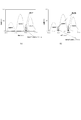
- FIG. 1 is a schematic configuration diagram of a projector according to an embodiment of the present invention. It is an enlarged view of the TIR prism shown in FIG. It is a figure which shows the reflective film characteristic provided in the O surface shown in FIG. It is a figure which shows the reflective film characteristic provided in the O surface shown in FIG. It is explanatory drawing in the case of utilizing the angle characteristic of the TIR prism shown in FIG. It is another schematic block diagram of the projector of embodiment which concerns on this invention. It is a figure which shows a mode that the light on the screen shown in FIG. 1 is guide
- FIG. 5 is a diagram showing the reflection characteristics of the O surface shown in FIG. 4 together with the wavelength characteristics of the light emitting element.
- FIG. 10 It is a functional block diagram which shows the structure of the projector shown in FIG. It is a figure which shows a mode that the light emitting element was irradiated to the projection image projected on the screen. It is a figure which shows the captured image by which the light spot of the light emitting element shown in FIG. 10 was imaged. It is a figure which shows the OSD image which the OSD drawing part shown in FIG. 9 produces
- the TIR prism that separates the illumination light and the projection light is also used for the separation of the projection light and the imaging light for imaging, thereby reducing the number of components when realizing the imaging function. be able to.
- a projector 100 includes a lamp 1, a color wheel 2, a rod integrator 3, a condenser lens 4, a TIR (Total Internal Reflection) prism 5, a DMD 6, a projection lens 7, a magnification correction optical system 10, and an image sensor 11. And.
- Illumination light emitted from the lamp 1 that is a light source enters the color wheel 2.
- the color wheel 2 has red, blue, and green filters and is driven by a motor (not shown) to rotate at high speed. As the color wheel 2 rotates, the three color filters are switched in a short time. As a result, the illumination light is color-separated into three colors of R (red) light, B (blue) light, and G (green) light in a time-sharing manner. Each separated color light sequentially enters the rod integrator 3.
- the rod integrator 3 is a quadrangular prism lens made of glass or the like, and totally reflects incident light internally to emit light having a uniform illuminance distribution.
- the light emitted from the rod integrator 3 is guided by the condenser lens 4 composed of a plurality of lenses so as to be irradiated on the DMD 6 with an appropriate size, and enters the TIR prism 5.
- the TIR prism 5 includes a first prism 5a and a second prism 5b, and a reflecting surface is formed at the boundary between the two prisms.
- the incident light from the condenser lens 4 on the reflecting surface provided inside the TIR prism 5 is totally reflected and guided to the DMD 6 because the incident angle is not less than the critical angle.
- the DMD 6 is a type of light modulation element (light valve) in which a large number of micromirrors are arranged in a plane.
- the DMD 6 spatially modulates red, green, and blue light irradiated in a time-sharing manner based on an image signal from the outside to generate projection light.
- the projection light from the DMD 6 enters the reflection surface of the TIR prism 5 at an incident angle smaller than the critical angle. Therefore, the projection light from the DMD 6 passes through the reflection surface and enters the projection lens 7.
- the projection light is enlarged and projected by the projection lens 7 and forms an image on the screen 8.
- the user can point to an arbitrary position on the screen 8 through the light emitting element 9 that emits infrared light or the like.
- the light reflected by the screen 8 enters the TIR prism 5 via the projection lens 7.
- the light from the screen 8 that has entered the TIR prism 5 is reflected by the reflection surface of the TIR prism 5, is reflected inside the TIR prism 5, and is emitted from the TIR prism 5.
- the light emitted from the TIR prism 5 is guided to an image sensor 11 composed of a CCD (Charge Coupled Device), a CMOS (Complementary Metal Oxide Semiconductor), or the like through a plurality of lenses that are the magnification correction optical system 10 for imaging. An image is formed on the element 11.
- CCD Charge Coupled Device
- CMOS Complementary Metal Oxide Semiconductor
- an irradiation position of infrared light on the screen 8 is detected by an image processing unit to be described later, and a pointing image indicating that the user is pointing is projected on the screen 8 via the DMD 6 and fed back. Etc. are performed.
- the plurality of lenses that are the magnification correction optical system 10 include the TIR prism 5 when the size of the DMD 6 and the size of the image sensor 11 do not match or when the projection system and the imaging system need to have different magnifications.
- the image sensor 11 may be inserted. That is, when the size of the DMD 6 and the size of the image sensor 11 are equal, or when the projection system and the imaging system do not need to have different magnifications, the cost can be reduced by omitting the magnification correction optical system 10. .
- the illumination light and the projection light are separated by the TIR prism 5, and the projection light and the imaging light for imaging are separated.
- Imaging light for imaging (light from the screen 8 side) is guided to the imaging device 11 using a surface of the TIR prism 5 which is not normally used. For this reason, it is not necessary to provide an additional part for the imaging function, so that it is possible to reduce the cost and size of the product, prevent deterioration of optical performance, and the like.
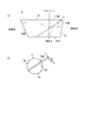
- FIG. 2 is an enlarged view of the TIR prism 5.
- the TIR prism 5 includes a first prism 5a and a second prism 5b.
- FIG. 2B is an enlarged view of ⁇ shown in FIG.
- the I surface of the first prism 5a and the O surface of the second prism 5b are arranged in parallel with a gap of several ⁇ m.
- the illumination light from the lamp 1 is incident on the A surface of the first prism 5a through the illumination optical system such as the condenser lens 4, and is reflected by the I surface of the first prism 5a and from the B surface of the first prism 5a. It emits toward the DMD 6.
- the illumination light is optically modulated by the DMD 6 and is incident from the B surface of the first prism 5a as projection light.
- the projection light incident from the B surface exits from the I surface of the first prism 5a, enters the O surface of the second prism 5b, exits from the C surface of the second prism 5b, and passes through the projection lens 7 to the screen. 8 is imaged.
- the light reflected by the screen 8 is incident from the C surface of the second prism 5b through the projection lens 7, is reflected by the O surface of the second prism 5b, and is reflected by the second prism 5b through the internal reflection.
- the light is emitted from the D surface of 5b toward the image sensor 11. Needless to say, the light reflected by the O-plane of the second prism 5b does not need to go through the internal reflection of the second prism 5b as long as the imaging element 11 is disposed on the optical path.
- the TIR prism 5 is shown as an example composed of a first prism 5a having a triangular surface and a second prism 5b having a quadrangular surface. .
- the TIR prism 5 has a reflecting surface formed to reflect the illumination light and guide it to the DMD 6 and to transmit the light reflected by the DMD 6 and output it to the projection lens 7. It is only necessary that the light incident from the lens 7 can be reflected and guided to the image sensor 11.
- the light reflected by the screen 8 enters through the projection lens 7 from the C surface of the first prism 5b and is reflected by the O surface. At this time, light in the range of L in the drawing is reflected on the O plane.
- the range of L corresponds to the screen area by DMD6.
- the light reflected by the O plane is internally reflected by the C plane and reaches the D plane.
- the light that reaches the D surface passes through the D surface, is guided to the image sensor 11 through the magnification correction optical system 10, and is taken into the image sensor 11.
- This D plane is installed perpendicular to the optical axis of the imaging light for imaging (imaging light) guided to the imaging device 11 (light at the center of the captured image).
- the TIR prism 5 side of the magnification correction optical system 10 is a telecentric optical system. That is, the telecentricity is maintained up to the magnification correction optical system 10 which is a correction lens on the image pickup device 11 side.
- the DMD 6 side of the projection lens 7 is similarly telecentric in a normal design. Therefore, it becomes possible to efficiently guide the imaging light over the entire area of the screen onto the imaging element 11.
- the D plane is installed perpendicular to the optical axis of the imaging light, so that symmetry with respect to the optical axis is maintained, and aberrations caused by the inclination of the optical axis do not occur. That is, astigmatism that occurs when a non-telecentric ray passes through the D surface of the TIR prism does not occur in principle. Therefore, the captured image becomes sharp and the uniformity of the entire captured image is maintained.
- NA aperture
- telecentricity is required as shown in the figure. It is more efficient to maintain.
- FIG. 3 is a spectral reflectance characteristic diagram of the O-plane.
- a is a reflectance characteristic when a normal visible light AR coating (antireflection film) is provided on the O surface. Since the AR coat reflects infrared rays (around 900 nm) by about 40%, an optical system can be established.
- a film specially designed in accordance with this embodiment so as to increase the reflectance with respect to infrared rays may be provided on the O plane. In this case, the film shown in b reflects about 80% of infrared rays and has an infrared reflectance about twice that of the AR coating shown in a.
- the projection lens 7 needs to transmit infrared rays from the screen 8 and guide it to the O plane.
- the projection lens 7 is often composed of a plurality of lenses, and the transmittance of infrared rays falls while passing through each lens. Therefore, the projection lens 7 may be provided with a film specially designed to transmit infrared rays instead of the AR coat.
- the film “a” or “b” shown in FIG. 3 reflects the visible light to the image pickup device 11 by using the reflectance with respect to visible light (near 400 nm to 700 nm) existing at several% on the O plane. May be.
- the visible light in the valleys between the R, G, and B projection light spectra may be reflected and guided to the image sensor 11.
- the reflection characteristics of the film provided on the O surface for reflecting visible light are indicated by solid lines, and the output characteristics of the R, G, and B projection light are indicated by dotted lines for reference.
- the film provided on the O plane is designed to have a high reflectance in the vicinity of 600 nm, which is a valley between the spectra of the G projection light and the R projection light.
- the projection light from the DMD 6 side is transmitted through the O plane, and the visible light near the valley of the spectrum of the G projection light and the R projection light among the light from the screen 8 side is reflected by the O plane. it can.
- the projection light and the imaging light (light from the screen 8) can be efficiently separated, and the light from the screen 8 can be guided to form an image on the image pickup device 11.
- membrane provided in O surface is 500 nm vicinity used as the valley of the spectrum of B projection light and G projection light, and the valley of the spectrum of G projection light and R projection light It may be designed so that both the reflectances in the vicinity of 600 nm become high, or any one of the reflectances may be designed to be high.
- the film provided on the O plane is designed to reflect a wavelength band near the valley of the spectrum of the G, B, and R projection light. Therefore, as shown in FIG. 8, the projected image is affected by overlapping the wavelength band (hatched area in the figure) of the light emitting element 9 that is a pointing device with the wavelength band in which the reflectance of the O-plane film is increased. Instead, the light of the light emitting element 9 reflected by the screen 8 is guided to the image sensor 11. Therefore, an image processing unit to be described later can acquire the irradiation position information of the light emitting element 9.
- 8A corresponds to FIG. 4A
- FIG. 8B corresponds to FIG. 4B.
- the light-emitting element 9 having a wavelength in the vicinity of 500 nm and the vicinity of 600 nm can be used.
- a color filter that transmits, for example, in a time-division manner a wavelength that matches the wavelength band (near 500 nm and near 600 nm) of the two light emitting elements 9 may be provided on the imaging element 11 side.
- the image pickup device 11 a color type device that matches the color filter, two light emitting devices 9 having different wavelength bands can be used simultaneously on the screen 8 without interfering with each other.
- FIG. 9 is a functional block diagram illustrating the configuration of the projector 100.
- the projector 100 includes an imaging unit 22, an image processing unit 20, a DMD 6, and an optical unit 21.
- the imaging unit 22 is a camera or the like, and includes the imaging element 11.
- the optical unit 21 includes the lamp 1, the color wheel 2, the rod integrator 3, the condenser lens 4, the TIR prism 5, the projection lens 7, and the magnification correction optical system 10.
- the imaging unit 22 outputs the captured image captured by the imaging element 11 to the image processing unit 20 at predetermined time intervals or continuously.
- the captured image the light spot of the light emitting element 9 indicating the position where the user irradiates the screen 8 with the light emitting element 9 is captured.
- the image processing unit 20 includes an irradiation position detection unit 201, an OSD drawing unit 202, a signal processing unit 203, a video input unit, and an image composition unit 204.
- the irradiation position detection unit 201 Each time the irradiation position detection unit 201 acquires a captured image from the imaging unit 22, the irradiation position detection unit 201 detects the position of the light spot in the captured image, for example, based on a luminance change in the captured image. The irradiation position detection unit 201 outputs the detected light spot position, that is, irradiation position information, to the OSD drawing unit 202.
- the OSD drawing unit 202 generates an OSD image drawn so that a pointing image such as an arrow overlaps the irradiation position on the screen 8 by the light emitting element 9 based on the irradiation position information.
- the signal processing unit 203 acquires a video signal (image signal) from, for example, an external memory (not shown) or a computer. Then, the signal processing unit 203 performs image adjustment so that the acquired video signal becomes an image suitable for projection, and outputs the image signal to the image composition unit 204.
- a video signal image signal
- the signal processing unit 203 performs image adjustment so that the acquired video signal becomes an image suitable for projection, and outputs the image signal to the image composition unit 204.
- the image combining unit 204 combines the OSD image acquired from the OSD drawing unit 202 and the video signal acquired via the signal processing unit 203. Thereby, a composite image in which the pointing image is combined with the video signal is generated.
- the image composition unit 204 outputs the generated composite image to the DMD 6.
- the DMD 6 projects the composite image acquired from the image composition unit 204 on the screen 8 via the optical unit 21. As a result, a projection image in which the irradiation position of the light emitting element 9 and the pointing image are overlapped is displayed on the screen 8.
- the user irradiates the projected image on the screen 8 with infrared light or the like using the light emitting element 9 and points to an arbitrary place on the projected image.
- the imaging unit 22 can receive only the wavelength of the light emitting element 9, only the light spot S representing the irradiation position of the imaging element 9 is imaged.
- the irradiation position detection unit 201 detects the light spot S based on, for example, a luminance change in the captured image. For example, when the size of the captured image is horizontal Lx and vertical Ly, the irradiation position detection unit 201 acquires the position of the light spot S as horizontal x and vertical y.
- the OSD drawing unit 202 generates an OSD image in which a pointing image is drawn based on the position information (irradiation position information) of the light spot S acquired from the irradiation position detection unit 201. For example, as shown in FIG. 12, when the resolution of the DMD 6 is XGA, the OSD image area of the OSD drawing unit 202 is 1024 ⁇ 768. In this case, the OSD drawing unit 202 generates an OSD image in which the pointing image P is drawn at a position of horizontal 1024 ⁇ (x / Lx) and vertical 768 ⁇ (y / Ly) on the OSD image area. The OSD drawing unit 202 outputs the generated OSD image to the image composition unit 204.
- the image composition unit 204 generates a composite image obtained by combining the OSD image and the video signal. This composite image is projected onto the screen 8 via the DMD 6 and the optical unit 21. Then, as shown in FIG. 14, a projection image in which the pointing image P is superimposed on the irradiation position of the light emitting element 9 is displayed on the screen 8.
- the pointing image P can be arbitrarily changed by the user. Further, the pointing image P includes not only illustrations and figures but also images representing the locus of the irradiation position of the light emitting element 9 as a line. Further, the image processing unit 20 may feed back the irradiation position information detected by the irradiation position detection unit 201 to an external computer or the like that inputs a video signal so that the mouse operation of the screen by the light emitting element 9 can be performed. That is, the projector 100 may function as an interactive projector having an electronic blackboard function. Further, the image processing unit 20 may store the synthesized image generated by the image synthesizing unit 204 in a memory (not shown) so that it can be projected again.
- the projection light and the imaging light can be separated by providing an appropriately designed reflective film on the O plane, but this can also be realized by adjusting the angle characteristics of the O plane.
- FIG. 5 is an explanatory diagram in the case where the angle characteristic of the TIR prism 5 is used.
- FIG. 5 shows an arrangement relationship between the projection light, the effective light range for the image sensor 11 and the boundary indicating the critical angle in the projection lens entrance pupil when the projection lens 7 is viewed from the DMD 6 side.
- FIG. When using visible light, it can be separated by arranging the projection light, the imaging light, and the critical angle as shown in the figure.
- the angle of the reflection surface at this time depends on the aperture (NA) required on the image sensor 11 side, but if there is sufficient sensitivity, the smaller the shift angle, the smaller the loss of projection light, which is advantageous. . In order to improve the contrast, it may be shifted by 2 to 3 degrees, and this range is the best.
- NA aperture
- a stop having an aperture that is biased with respect to the optical axis on the illumination light side may be disposed in the vicinity of the secondary light source image. According to this method, light can be guided to the imaging device 11 over the entire visible light range, and full colorization is possible. In order to achieve full color, a film that transmits the projection light from the DMD 6 side and totally reflects the light for the image sensor 11 from the screen 8 side may be provided on the reflection surface.
- the single-plate projector 100 having the DMD 6 is described.
- the projector may be a multi-panel projector.
- the three-plate projector 101 shown in FIG. 6 instead of the color wheel 2 and the DMD 6 shown in FIG. 1, red, green, and blue respectively generated by the R DMD 13, the G DMD 14, and the B DMD 15 are used.
- the image is synthesized via the Philips prism 12 and projected onto the screen 8.
- the optical path of the illumination light guided to the R DMD 13, the G DMD 14, and the B DMD 15 is omitted, but is assumed to be appropriately designed and arranged.
- Lamp 2 Color wheel 3: Rod integrator 4: Condenser lens 5: TIR prism 5a: first prism 5b: Second prism 6: DMD 7: Projection lens 8: Screen 9: Light emitting element 10: Magnification correction optical system 11: Image sensor 12: Philips prism 13: DMD for R 14: DMD for G 15: DMD for B 20: Image processing unit 21: Optical unit 22: Imaging unit 201: Irradiation position detection unit 202: OSD drawing unit 203: Signal processor 204: Image composition unit S: Light spot P: Pointing image 100, 101: Projector
Landscapes
- Engineering & Computer Science (AREA)
- Physics & Mathematics (AREA)
- General Physics & Mathematics (AREA)
- General Engineering & Computer Science (AREA)
- Theoretical Computer Science (AREA)
- Human Computer Interaction (AREA)
- Optics & Photonics (AREA)
- Multimedia (AREA)
- Signal Processing (AREA)
- Projection Apparatus (AREA)
- Controls And Circuits For Display Device (AREA)
- Transforming Electric Information Into Light Information (AREA)
- Optical Elements Other Than Lenses (AREA)
- Mechanical Light Control Or Optical Switches (AREA)
- Optical Filters (AREA)
Abstract
撮像機能を備えたプロジェクタの構成部品数を減らすことができる技術を提供する。ランプ(1)からの照明光は、照明光学系を介してTIRプリズム(5)の第1の面から入射し、内部の反射面で反射してTIRプリズム(5)の第2の面から出射し、DMD(6)により光変調されて投射光としてTIRプリズム(5)の第2の面に入射する。DMD(6)からの投射光は、TIRプリズム(5)の反射面を透過してTIRプリズム(5)の第3の面から射出し、投射レンズ(7)で拡大投射されてスクリーン(8)上に結像する。発光素子(9)の光は、スクリーン(8)で反射して、投射レンズ(7)を介してTIRプリズム(5)の第3の面に入射し、内部の反射面で反射してTIRプリズム(5)の第4の面から出射し、撮像素子(11)上で結像する。
Description
本発明は、撮像機能を備えたプロジェクタに関する。
従来、プロジェクタの中には、スクリーン側からの光を撮像素子上に結像させる撮像機能を備え、ポインティングデバイス機能や撮影機能等の付加機能に用いるものがある。このようなプロジェクタにおいては、DMD(Digital Micromirror Device)等の画像表示素子による画像をスクリーンに拡大投射する投射レンズを、スクリーン側からの光を撮像素子に導くための結像手段として兼用する技術がある。
例えば、特許文献1の技術では、DMDによって光変調された画像をTIRプリズムを介して第1のレンズ群で集光し、分離ミラーで反射させて、第3のレンズ群によりスクリーンに投射している。そして、特許文献1の技術では、スクリーン上を指し示した赤外線発光ダイオードからの光を第3のレンズ群により分離ミラーへ導き、分離ミラーの入射面に設けられた波長選択膜により赤外線発光ダイオードからの光を透過させて、第2のレンズ群を介して撮像素子上に結像させている。
しかしながら、特許文献1に記載の技術では、DMDによる投射光とスクリーンからの光とを分離するために分離ミラーを追加部品として設けている。そのため、特許文献1の技術では、追加部品そのものや保持のための補助的な部品も含め、コストアップや製品サイズアップとなっていた。また、特許文献1の技術では、この追加部品を挿入する空間によってレンズ群間に一定の空間が必要となり、光学設計上の制約となって、光学性能の劣化やレンズ枚数の増加となっていた。更に、特許文献1の技術では、この追加部品により反射や透過損失が増え、投射光の光出力が低下するとともに、斜めに挿入された分離ミラーの平行平板による非点収差が発生して、結像性能を劣化させていた。
また、特許文献1の技術では、追加部品を設けて撮像機能を実現しているため、共通プラットフォームで撮像機能無しの製品を展開する場合も、追加部品やそれに伴う光学設計上のレンズ枚数の増加等による余分なコストが生じていた。そのため、特許文献1の技術では、共通プラットフォームで撮像機能有り無しの製品を展開しにくく、投資効率が悪かった。
本発明は上記課題に鑑みてなされたものであり、撮像機能を備えたプロジェクタの構成部品数を減らすことができる技術を提供することを目的とする。
本発明のプロジェクタは、光源からの光を反射させて光変調素子に導くと共に、前記光変調素子で反射した光を透過させて投射光学系へ出力するTIRプリズムを備えたプロジェクタであって、前記投射光学系から前記TIRプリズムの反射面に入射した光の反射方向に撮像素子が配置されたことを特徴とする。
また、前記反射面には、赤外線光を反射させる膜が設けられていてもよい。
また、前記反射面には、投射光のスペクトルで谷になる部分の反射率が高くなる膜が設けられていてもよい。
また、前記反射面は、角度特性によって、前記光変調素子で反射した光を透過させて前記投射光学系へ出力すると共に、前記投射光学系から入射した光を反射させて前記撮像素子に導いてもよい。
また、スクリーンに照射された発光素子の光が、前記投射光学系を介して前記TIRプリズムの前記反射面で反射して、前記TIRプリズムの前記撮像素子が配置された側の面を射出して、前記撮像素子上で結像してもよい。
また、前記TIRプリズムの前記撮像素子が配置された側の面は、撮影像のセンターの光に対して垂直になっていてもよい。
また、前記反射面に設けられた膜の反射特性の中で反射率が高い波長帯域とスクリーンを照射する発光素子の波長帯域とが重なっていてもよい。
また、前記撮像素子で撮像された撮像画像から発光素子のスクリーン上の照射位置を示す照射位置情報を取得する照射位置検出部と、前記照射位置情報に対応して所定のポインティング画像を描画したOSD画像を生成するOSD描画部と、前記OSD画像と前記投射光学系を介してスクリーンに投影される投影画像とを合成して合成画像を生成する画像合成部と、前記合成画像を投影するように光変調して前記TIRプリズムに射出する前記光変調素子とを備えてもよい。
本発明によれば、撮像機能を備えたプロジェクタの構成部品数を減らすことができる。
本実施形態のプロジェクタは、照明光と投射光とを分離するTIRプリズムを、投射光と撮像用の結像光との分離に兼用することで、撮像機能を実現する際の構成部品数を減らすことができる。以下、図を参照して本発明の実施形態を詳細に説明する。
図1に示すように、プロジェクタ100は、ランプ1とカラーホイール2とロッドインテグレータ3とコンデンサーレンズ4とTIR(Total Internal Reflection)プリズム5とDMD6と投射レンズ7と倍率補正光学系10と撮像素子11とを備えている。
光源であるランプ1から出射された照明光は、カラーホイール2に入射する。
カラーホイール2は、赤、青、緑のフィルタを有し、不図示のモータにより駆動されて高速で回転する。カラーホイール2が回転することで、3色のフィルタが短時間で切り替わる。これにより、照明光がR(赤色)光、B(青色)光、G(緑色)光の3色に時分割で色分離される。分離された各色光は、順次ロッドインテグレータ3に入射する。
ロッドインテグレータ3は、四角柱状のガラス製等のレンズであり、入射光を内部で全反射させて照度分布が均一な光を出射する。ロッドインテグレータ3から出射した光は、複数のレンズで構成されるコンデンサーレンズ4により、DMD6上に適切なサイズで照射されるように導かれ、TIRプリズム5に入射する。
TIRプリズム5は、第1プリズム5aと第2プリズム5bとで構成されており、2つのプリズムの境界に反射面が形成されている。このTIRプリズム5の内部に設けられた反射面に対するコンデンサーレンズ4からの入射光は、入射角が臨界角以上であるため、全反射してDMD6に導かれる。
DMD6は、多数のマイクロミラーを平面に配列した光変調素子(ライトバルブ)の一種である。DMD6は、時分割されて照射される赤・緑・青の光を、外部からの画像信号に基づいて、空間的に光変調して投射光を生成する。DMD6による投射光は、TIRプリズム5の反射面に対して臨界角よりも小さい入射角で入射する。そのため、DMD6による投射光は、反射面を透過して投射レンズ7に入射する。投射光は、投射レンズ7により拡大投射されてスクリーン8上に結像する。
ユーザは、赤外線等を発光する発光素子9を介して、スクリーン8上の任意の位置を指し示すことができる。スクリーン8で反射した光は、投射レンズ7を介してTIRプリズム5に入射する。
TIRプリズム5に入射したスクリーン8からの光は、TIRプリズム5の反射面で反射するとともにTIRプリズム5の内部で反射して、TIRプリズム5から射出する。TIRプリズム5から射出した光は、倍率補正光学系10である複数のレンズを介して、CCD(Charge Coupled Device)やCMOS(Complementary Metal Oxide Semiconductor)等で構成される撮像素子11に導かれ、撮像素子11上で結像する。
これにより、後述する画像処理部により、スクリーン8上の赤外線光の照射位置を検出して、DMD6を介して、ユーザが指し示していることを示すポインティング画像等をスクリーン8上に投影し、フィードバックする等の処理が行われる。
なお、倍率補正光学系10である複数のレンズは、DMD6のサイズと撮像素子11のサイズとが一致しない場合や、投射系と結像系を別々の倍率にする必要がある場合にTIRプリズム5と撮像素子11との間に挿入されればよい。つまり、DMD6のサイズと撮像素子11のサイズとが一致する場合や、投射系と結像系を別々の倍率にする必要がない場合、倍率補正光学系10を省いてコストを削減することができる。
このように、本実施形態では、前面投射型のプロジェクタ100において、TIRプリズム5により照明光と投射光とを分離するとともに、投射光と撮像用の結像光とを分離している。撮像用の結像光(スクリーン8側からの光)は、TIRプリズム5の通常使用されていない面を使用して、撮像素子11へ導かれている。そのため、撮像機能のために追加部品を設けなくて済むので、製品のコストダウンやサイズダウン、光学性能の劣化防止等を実現することができる。
TIRプリズム5について詳細に説明する。
図2は、TIRプリズム5の拡大図である。図2(a)に示すように、TIRプリズム5は、第1プリズム5aと第2プリズム5bとで構成される。図2(b)は、図2(a)に示すαの拡大図である。図2(b)に示すように、TIRプリズム5は、第1プリズム5aのI面と第2プリズム5bのO面とが、数μmの間隙が設けられ平行に配置されている。
ランプ1からの照明光は、コンデンサーレンズ4等の照明光学系を介して第1プリズム5aのA面に入射し、第1プリズム5aのI面で反射して、第1プリズム5aのB面からDMD6に向けて出射する。DMD6により照明光は光変調され、投射光として第1プリズム5aのB面から入射する。B面から入射した投射光は、第1プリズム5aのI面を出射し、第2プリズム5bのO面に入射して、第2プリズム5bのC面から出射し、投射レンズ7を介してスクリーン8上で結像する。
スクリーン8で反射した光は、投射レンズ7を介して第2プリズム5bのC面から入射し、第2プリズム5bのO面で反射して、第2プリズム5bの内部反射を介して第2プリズム5bのD面から撮像素子11に向けて出射する。なお、第2プリズム5bのO面で反射した光は、その光路上に撮像素子11が配置されていれば、第2プリズム5bの内部反射を介さなくてもよいことは言うまでもない。
つまり、第1プリズム5aのI面では、光源側から入射した照明光を反射させてDMD6に入射させると共に、DMD6で光変調された投影画像を透過させてO面に導いている。また、第2プリズム5bのO面では、I面側から入射したDMD6の投影画像を透過させると共に、スクリーン8側から入射した光を反射させ、第2プリズム5b内で反射させて撮像素子11に導いている。なお、図示では、TIRプリズム5は、3角面を有する第1プリズム5aと4角面を有する第2プリズム5bとで構成される例を示しているが、これに限らず他の形でもよい。言い換えれば、TIRプリズム5は、照明光を反射させてDMD6に導くと共に、DMD6で反射した光を透過させて投射レンズ7に出力するように形成された反射面を有し、この反射面により投射レンズ7から入射した光を反射させて撮像素子11に導くことができればよい。
具体的に、図7を参照して、スクリーン8上の光が、撮像素子11に導かれる様子を説明する。スクリーン8で反射した光は、投射レンズ7を介して、第1プリズム5bのC面から入射してO面で反射する。このとき、O面では、図示でLの範囲の光が反射する。このLの範囲は、DMD6による画面領域に対応している。そして、O面で反射した光は、C面で内部反射してD面に達する。D面に達した光は、D面を透過し、倍率補正光学系10を介して撮像素子11に導かれ、撮像素子11に取り込まれる。
このD面は、撮像素子11に導かれる撮像用の結像光(撮像光)の光軸(撮影像のセンターの光)に対して垂直に設置されている。また、図示では、倍率補正光学系10のTIRプリズム5側がテレセントリックとなる光学系となっている。つまり、撮像素子11側の補正レンズである倍率補正光学系10までは、テレセントリックを維持した形になっている。この場合、投射レンズ7のDMD6側は、通常の設計において、同様にテレセントリックである。そのため、撮像光を画面内全域に亘って効率良く撮像素子11上に導くことが可能となる。
また、このように、D面が撮像光の光軸に対して垂直に設置されることにより、光軸に対する対称性が保たれ、光軸の傾きにより生じる収差が発生しなくなる。つまり、非テレセントリックな光線がTIRプリズムのD面を通ることで発生する非点収差が、原理的に発生しなくなる。そのため、撮像画像がシャープになるとともに、撮像画像全体の均一性が保たれる。
なお、撮像素子11側のNA(開口)が十分小さい場合には、必ずしもテレセントリックである必要がないが、撮像素子11側のNAを大きくして感度を上げるためには、図示のようにテレセントリックを維持するほうが効率がよい。
また、このとき、第2プリズム5bのO面は、発光素子9の波長である赤外線を効率良く反射させて撮像素子11に導くことができればよい。図3は、O面の分光反射率特性図である。aは、通常の可視光用のARコート(反射防止膜)をO面に設けた場合の反射率特性である。ARコートは、赤外線(900nm付近)を約40%反射するため、光学系を成立させることができる。また、bに示すように、赤外線に対する反射率を上げるように本実施形態に合わせて特別に設計した膜をO面に設けてもよい。この場合、bに示す膜では、赤外線を約80%反射し、aに示すARコートの約2倍の赤外線反射率となっている。
なお、投射レンズ7は、スクリーン8からの赤外線を透過させてO面に導く必要がある。投射レンズ7は、複数枚のレンズで構成されることが多く、各レンズを透過する内に赤外線の透過率が落ちてしまう。そのため、投射レンズ7には、ARコートではなく、赤外線を透過させるよう特別に設計された膜を設ければよい。
また、赤外線だけでなく、可視光が撮像素子11に導かれるようにしてもよい。この場合、図3に示すa又はbの膜は、O面に数%存在する可視光(400nm~700nm付近)に対する反射率を利用して、可視光を反射させて撮像素子11に導くようにしてもよい。
また、R,G,Bの各投射光のスペクトル間で谷になる部分の可視光が反射して、撮像素子11に導かれるようにしてもよい。図4では、可視光を反射させるためにO面に設けられた膜の反射特性を実線で示し、参考として点線でR,G,Bの各投射光の出力特性を示している。
図4(a)では、O面に設けられた膜は、G投射光とR投射光とのスペクトルの谷間となる600nm付近の反射率が高くなるように設計されている。これにより、DMD6側からの投射光をO面で透過させるとともに、スクリーン8側からの光の内、G投射光とR投射光とのスペクトルの谷間付近の可視光をO面で反射させることができる。これにより、投射光と結像光(スクリーン8からの光)とを効率良く分離し、スクリーン8からの光を導いて撮像素子11上で結像させることができる。
なお、図4(b)に示すように、O面に設けられる膜は、B投射光とG投射光とのスペクトルの谷間となる500nm付近、及びG投射光とR投射光とのスペクトルの谷間となる600nm付近の両方の反射率が高くなるように設計されてもよく、又、そのいずれかの反射率が高くなるように設計されてもよい。
つまり、O面に設けられた膜は、G、B、R投射光のスペクトルの谷間付近の波長帯域を反射させるように設計されている。そのため、図8に示すように、ポインティングデバイスである発光素子9の波長帯域(図示で斜線領域)とO面の膜の反射率を上げた波長帯域とを重ねることにより、投射画像に影響されることなく、スクリーン8で反射した発光素子9の光が撮像素子11に導かれる。そのため、後述の画像処理部が、発光素子9の照射位置情報を取得することができる。なお、図8(a)は、図4(a)に対応しており、図8(b)は、図4(b)に対応している。
また、図8(b)に示すように、O面の膜が500nm付近と600nm付近の両方の反射率が高くなるように設計されている場合、500nm付近の波長の発光素子9と600nm付近の波長の発光素子9とを両方使用することができる。この場合、撮像素子11側に2つの発光素子9の波長帯域(500nm付近と600nm付近)と一致する波長を例えば時分割で透過させるカラーフィルターを設ければよい。このように、撮像素子11をカラーフィルターに合わせたカラータイプの素子にすることによって、波長帯域の異なる2つの発光素子9が、互いに干渉せずにスクリーン8上で同時に使用可能となる。
次に、図9を参照して、画像処理部によって、発光素子9の照射位置が検出され、ポインティング画像がスクリーン8に投影される処理について説明する。
図9は、プロジェクタ100の構成を示す機能ブロック図である。図示では、プロジェクタ100は、撮像部22と画像処理部20とDMD6と光学ユニット21とを備えている。なお、ここで、撮像部22は、カメラ等であり、撮像素子11を含んでいる。また、光学ユニット21は、ランプ1とカラーホイール2とロッドインテグレータ3とコンデンサーレンズ4とTIRプリズム5と投射レンズ7と倍率補正光学系10とを含んでいるものとする。
撮像部22は、撮像素子11で撮像された撮像画像を所定時間毎に又は連続して画像処理部20に出力する。撮像画像には、ユーザが発光素子9を用いてスクリーン8上を照射した位置を示す発光素子9の光点が撮像されている。
画像処理部20は、照射位置検出部201とOSD描画部202と信号処理部203と映像入力部と画像合成部204とを備えている。
照射位置検出部201は、撮像部22から撮像画像を取得するたびに、例えば、撮像画像内の輝度変化に基づいて、撮像画像における光点の位置を検出する。照射位置検出部201は、検出した光点の位置、即ち照射位置情報をOSD描画部202に出力する。
OSD描画部202は、照射位置情報に基づいて、発光素子9によるスクリーン8上の照射位置に、例えば矢印等のポインティング画像が重なるように描画したOSD画像を生成する。
信号処理部203は、例えば不図示の外部メモリやコンピュータ等から映像信号(画像信号)を取得する。そして、信号処理部203は、取得した映像信号に対して、投影に適した画像となるように画像調整を行って、画像合成部204に出力する。
画像合成部204は、OSD描画部202から取得したOSD画像と、信号処理部203を介して取得した映像信号とを合成する。これにより、映像信号にポインティング画像が合成された合成画像が生成される。画像合成部204は、生成した合成画像をDMD6に出力する。
DMD6は、光学ユニット21を介して、画像合成部204から取得した合成画像をスクリーン8上に投影させる。その結果、スクリーン8上には、発光素子9の照射位置とポインティング画像とが重なった投影画像が表示される。
具体的に、図10~図14を参照して、スクリーン8上の発光素子9の照射位置にポインティング画像が重なって投影される様子を説明する。
図10に示すように、ユーザが、スクリーン8上の投影画像に発光素子9を用いて赤外線光等を照射し、投影画像上の任意の場所を指し示したとする。すると、図11に示すように、撮像部22では、発光素子9の波長のみを受光可能であるため、撮像素子9の照射位置を表す光点Sのみが撮像される。照射位置検出部201は、例えば撮像画像内の輝度変化に基づいて、光点Sを検出する。そして、照射位置検出部201は、例えば、撮像画像のサイズが、横Lx、縦Lyであるときに、光点Sの位置を、横x、縦yとして取得する。
OSD描画部202は、照射位置検出部201から取得した光点Sの位置情報(照射位置情報)に基づいて、ポインティング画像を描画したOSD画像を生成する。例えば、図12に示すように、DMD6の解像度がXGAである場合、OSD描画部202のOSD画像領域は横1024×縦768となる。この場合、OSD描画部202は、OSD画像領域上の横1024×(x/Lx)、縦768×(y/Ly)の位置にポインティング画像Pを描画したOSD画像を生成する。OSD描画部202は、生成したOSD画像を画像合成部204に出力する。
図13に示すように、画像合成部204は、OSD画像と映像信号とを合成した合成画像を生成する。この合成画像が、DMD6、光学ユニット21を介してスクリーン8上に投影される。すると、図14に示すように、スクリーン8上には、発光素子9の照射位置にポインティング画像Pが重なった投影画像が表示される。
なお、ポインティング画像Pは、ユーザが任意に変更できるものとする。また、ポインティング画像Pには、イラストや図形だけでなく、発光素子9の照射位置の軌跡を線として表すものも含まれる。また、画像処理部20は、映像信号を入力する外部のコンピュータ等に照射位置検出部201で検出した照射位置情報をフィードバックして、発光素子9による画面のマウス操作を行えるようにしてもよい。つまり、プロジェクタ100は、電子黒板機能を備えたインタラクティブなプロジェクタとして機能してもよい。また、画像処理部20は、画像合成部204で生成した合成画像を不図示のメモリに記憶して、再び投影できるようにしてもよい。
なお、上記のように、適切に設計された反射膜をO面に設けることで投射光と結像光とを分離させることができるが、O面の角度特性を調整することによっても実現できる。
図5は、TIRプリズム5の角度特性を利用する場合の説明図である。具体的には、図5は、DMD6側から投射レンズ7を見たときの投射レンズ入射瞳における、投射光と撮像素子11用の有効光範囲と臨界角を示す境界との配置関係を示した図である。可視光を利用する場合、投射光、結像光、臨界角が図示のようになるように配置することにより分離することも可能である。このときの反射面の角度としては、撮像素子11側で必要とする開口(NA)にもよるが、十分な感度があればできるだけずらし角度が、小さいほうが投射光の損失が小さくなり有利となる。なお、コントラスト改善のため、2~3度ずらすことがあり、この範囲であれば最もよい。また、反射面であるI面に入射する照明光側の光軸の角度によっては、二次光源像近傍に照明光側の光軸に対して偏った開口を有する絞りを配置するとよい。この方法によれば、可視光全域に亘り撮像素子11へ光を導くことができ、フルカラー化が可能となる。なお、フルカラー化のため、DMD6側からの投射光を透過させ、スクリーン8側からの撮像素子11用の光を全反射させる膜を反射面に設けてもよい。
また、上記では、DMD6が1つの単板方式のプロジェクタ100について説明したが、プロジェクタは複数パネル方式であってもよい。例えば、図6に示す3板方式のプロジェクタ101の場合、図1に示すカラーホイール2及びDMD6に替えて、R用DMD13、G用DMD14、B用DMD15によって生成されたそれぞれ赤・緑・青の画像を、フィリップスプリズム12を介して合成し、スクリーン8上に投影している。なお、図6では、R用DMD13、G用DMD14、B用DMD15に導かれる照明光の光路を省略して示しているが、適宜設計配置されているものとする。
本発明は上述した実施の形態に限定されるものではなく、本発明の趣旨を逸脱しない範囲で種々様々に変更が可能であることは言うまでもない。なお、上記実施形態において、同様の機能を示す構成には、同一の符号を付してある。
1:ランプ
2:カラーホイール
3:ロッドインテグレータ
4:コンデンサーレンズ
5:TIRプリズム
5a:第1プリズム
5b:第2プリズム
6:DMD
7:投射レンズ
8:スクリーン
9:発光素子
10:倍率補正光学系
11:撮像素子
12:フィリップスプリズム
13:R用DMD
14:G用DMD
15:B用DMD
20:画像処理部
21:光学ユニット
22:撮像部
201:照射位置検出部
202:OSD描画部
203:信号処理部
204:画像合成部
S:光点
P:ポインティング画像
100,101:プロジェクタ
Claims (8)
-
光源からの光を反射させて光変調素子に導くと共に、前記光変調素子で反射した光を透過させて投射光学系へ出力するTIRプリズムを備えたプロジェクタであって、
前記投射光学系から前記TIRプリズムの反射面に入射した光の反射方向に撮像素子が配置された
ことを特徴とするプロジェクタ。
-
前記反射面には、赤外線光を反射させる膜が設けられていることを特徴とする請求項1に記載のプロジェクタ。
-
前記反射面には、投射光のスペクトルで谷になる部分の反射率が高くなる膜が設けられていることを特徴とする請求項1又は2に記載のプロジェクタ。
-
前記反射面は、角度特性によって、前記光変調素子で反射した光を透過させて前記投射光学系へ出力すると共に、前記投射光学系から入射した光を反射させて前記撮像素子に導くことを特徴とする請求項1から3までのいずれか一項に記載のプロジェクタ。
-
スクリーンに照射された発光素子の光が、前記投射光学系を介して前記TIRプリズムの前記反射面で反射して、前記TIRプリズムの前記撮像素子が配置された側の面を射出して、前記撮像素子上で結像することを特徴とする請求項1から4までのいずれか一項に記載のプロジェクタ。
-
前記TIRプリズムの前記撮像素子が配置された側の面は、撮影像のセンターの光に対して垂直になっていることを特徴とする請求項1から5までのいずれか一項に記載のプロジェクタ。
-
前記反射面に設けられた膜の反射特性の中で反射率が高い波長帯域とスクリーンを照射する発光素子の波長帯域とが重なっていることを特徴とする請求項1から6までのいずれか一項に記載のプロジェクタ。
-
前記撮像素子で撮像された撮像画像から発光素子のスクリーン上の照射位置を示す照射位置情報を取得する照射位置検出部と、
前記照射位置情報に対応して所定のポインティング画像を描画したOSD画像を生成するOSD描画部と、
前記OSD画像と前記投射光学系を介してスクリーンに投影される投影画像とを合成して合成画像を生成する画像合成部と、
前記合成画像を投影するように光変調して前記TIRプリズムに射出する前記光変調素子と
を備えたことを特徴とする請求項1から7までのいずれか一項に記載のプロジェクタ。
Priority Applications (2)
| Application Number | Priority Date | Filing Date | Title |
|---|---|---|---|
| CN201280071434.XA CN104204942A (zh) | 2012-03-14 | 2012-09-19 | 投影仪 |
| US14/384,990 US20150042564A1 (en) | 2012-03-14 | 2012-09-19 | Projector |
Applications Claiming Priority (4)
| Application Number | Priority Date | Filing Date | Title |
|---|---|---|---|
| JP2012056684 | 2012-03-14 | ||
| JP2012-056684 | 2012-03-14 | ||
| JP2012197403A JP5174273B1 (ja) | 2012-03-14 | 2012-09-07 | プロジェクタ |
| JP2012-197403 | 2012-09-07 |
Publications (1)
| Publication Number | Publication Date |
|---|---|
| WO2013136563A1 true WO2013136563A1 (ja) | 2013-09-19 |
Family
ID=48189359
Family Applications (1)
| Application Number | Title | Priority Date | Filing Date |
|---|---|---|---|
| PCT/JP2012/073882 Ceased WO2013136563A1 (ja) | 2012-03-14 | 2012-09-19 | プロジェクタ |
Country Status (4)
| Country | Link |
|---|---|
| US (1) | US20150042564A1 (ja) |
| JP (1) | JP5174273B1 (ja) |
| CN (1) | CN104204942A (ja) |
| WO (1) | WO2013136563A1 (ja) |
Families Citing this family (15)
| Publication number | Priority date | Publication date | Assignee | Title |
|---|---|---|---|---|
| WO2014141718A1 (ja) * | 2013-03-14 | 2014-09-18 | 日東光学株式会社 | 光学システムおよび光学システムを有する装置 |
| CN104977700B (zh) * | 2014-04-10 | 2018-08-10 | 长春理工大学 | 一种用于dmd相机的光学系统 |
| TWI575297B (zh) * | 2015-01-07 | 2017-03-21 | 佳世達科技股份有限公司 | 投影機 |
| CN104504945A (zh) * | 2015-01-12 | 2015-04-08 | 鲁杨 | 一种物理教学投影装置 |
| WO2017014317A1 (ja) * | 2015-07-23 | 2017-01-26 | コニカミノルタ株式会社 | 投影装置 |
| US11269117B2 (en) * | 2016-02-15 | 2022-03-08 | Konica Minolta, Inc. | Projection display apparatus |
| CN110221505A (zh) * | 2018-03-02 | 2019-09-10 | 台达电子工业股份有限公司 | 投影装置及投影方法 |
| CN108519152A (zh) * | 2018-04-11 | 2018-09-11 | 中科谱光科技(北京)有限公司 | 一种投影高光谱系统 |
| JP6974252B2 (ja) * | 2018-05-15 | 2021-12-01 | 京セラ株式会社 | 電磁波検出装置および情報取得システム |
| JP6974251B2 (ja) * | 2018-05-15 | 2021-12-01 | 京セラ株式会社 | 電磁波検出装置および情報取得システム |
| JP7712793B2 (ja) | 2021-05-17 | 2025-07-24 | パナソニックホールディングス株式会社 | 投写型映像表示装置 |
| JP7675561B2 (ja) | 2021-05-28 | 2025-05-13 | パナソニックホールディングス株式会社 | プリズムブロックおよび投写型映像表示装置 |
| WO2023149537A1 (ja) * | 2022-02-07 | 2023-08-10 | パナソニックIpマネジメント株式会社 | 投影撮像光学系及び投写型映像表示装置 |
| KR20230168859A (ko) * | 2022-06-08 | 2023-12-15 | 현대모비스 주식회사 | 자동차 조명 장치 및 그 작동 방법 |
| WO2024075748A1 (ja) * | 2022-10-05 | 2024-04-11 | パナソニックIpマネジメント株式会社 | プリズム群及び投写型映像表示装置 |
Citations (6)
| Publication number | Priority date | Publication date | Assignee | Title |
|---|---|---|---|---|
| JPH08339259A (ja) * | 1995-06-13 | 1996-12-24 | Sharp Corp | 投影表示装置 |
| JPH09282097A (ja) * | 1996-04-11 | 1997-10-31 | Toshiba Corp | 投写型液晶表示装置 |
| JPH09305312A (ja) * | 1996-05-15 | 1997-11-28 | Sharp Corp | 投影表示装置 |
| JPH11355696A (ja) * | 1998-06-05 | 1999-12-24 | Nec Corp | 画像表示装置及びプログラムを記録した記録媒体 |
| JP2008027080A (ja) * | 2006-07-19 | 2008-02-07 | Casio Comput Co Ltd | プレゼンテーションシステム |
| JP2009205442A (ja) * | 2008-02-28 | 2009-09-10 | Panasonic Corp | 画像投影装置 |
Family Cites Families (5)
| Publication number | Priority date | Publication date | Assignee | Title |
|---|---|---|---|---|
| US6707444B1 (en) * | 2000-08-18 | 2004-03-16 | International Business Machines Corporation | Projector and camera arrangement with shared optics and optical marker for use with whiteboard systems |
| AU2002365568A1 (en) * | 2001-11-28 | 2003-06-10 | 3M Innovative Properties Company | Tir prism for dmd projector |
| CN2921892Y (zh) * | 2006-06-23 | 2007-07-11 | 大恒新纪元科技股份有限公司光电研究所 | 用于dlp的投影光学系统 |
| FR2903199A1 (fr) * | 2006-06-30 | 2008-01-04 | Thomson Licensing Sas | Systeme optique pour projecteur et projecteur correspondant |
| CN202050475U (zh) * | 2011-04-15 | 2011-11-23 | 西安友米光电科技有限公司 | 投影、照相、摄像机一体式装置 |
-
2012
- 2012-09-07 JP JP2012197403A patent/JP5174273B1/ja not_active Expired - Fee Related
- 2012-09-19 US US14/384,990 patent/US20150042564A1/en not_active Abandoned
- 2012-09-19 CN CN201280071434.XA patent/CN104204942A/zh active Pending
- 2012-09-19 WO PCT/JP2012/073882 patent/WO2013136563A1/ja not_active Ceased
Patent Citations (6)
| Publication number | Priority date | Publication date | Assignee | Title |
|---|---|---|---|---|
| JPH08339259A (ja) * | 1995-06-13 | 1996-12-24 | Sharp Corp | 投影表示装置 |
| JPH09282097A (ja) * | 1996-04-11 | 1997-10-31 | Toshiba Corp | 投写型液晶表示装置 |
| JPH09305312A (ja) * | 1996-05-15 | 1997-11-28 | Sharp Corp | 投影表示装置 |
| JPH11355696A (ja) * | 1998-06-05 | 1999-12-24 | Nec Corp | 画像表示装置及びプログラムを記録した記録媒体 |
| JP2008027080A (ja) * | 2006-07-19 | 2008-02-07 | Casio Comput Co Ltd | プレゼンテーションシステム |
| JP2009205442A (ja) * | 2008-02-28 | 2009-09-10 | Panasonic Corp | 画像投影装置 |
Also Published As
| Publication number | Publication date |
|---|---|
| US20150042564A1 (en) | 2015-02-12 |
| JP5174273B1 (ja) | 2013-04-03 |
| JP2013218262A (ja) | 2013-10-24 |
| CN104204942A (zh) | 2014-12-10 |
Similar Documents
| Publication | Publication Date | Title |
|---|---|---|
| JP5174273B1 (ja) | プロジェクタ | |
| JP5531618B2 (ja) | 投写光学系およびプロジェクター | |
| US20160021351A1 (en) | Optical system and device having optical system | |
| US10419730B2 (en) | Image projection optical unit and projector | |
| JP6233419B2 (ja) | 3板式光学システム及びプロジェクター | |
| CN103852960A (zh) | 投影装置与聚光模组 | |
| US20160295181A1 (en) | Dlp pico-projector | |
| CN111837073B (zh) | 图像显示设备 | |
| JP2006065202A (ja) | 投写型画像表示装置 | |
| CN108700796B (zh) | 投射型显示装置 | |
| JP2004252112A (ja) | 映像投射装置及びこれに用いられる照明装置 | |
| US7261422B2 (en) | Display projection apparatus | |
| CN1892409B (zh) | 光学系统装置、以及具备该装置的投影型图像显示装置 | |
| JP6398513B2 (ja) | プリズムユニット及びプロジェクター | |
| US20100091246A1 (en) | Single projection display device | |
| WO2018030157A1 (ja) | 投射型表示装置 | |
| WO2016140049A1 (ja) | プリズムユニットおよびプロジェクター | |
| JP2017227747A (ja) | 投射型表示装置 | |
| JP2007293033A (ja) | プロジェクタ | |
| JP2020071474A (ja) | 光学系、画像投射装置および移動体 | |
| JP2014202881A (ja) | 照明光学系および投射型表示装置 | |
| WO2019163844A1 (ja) | 光学ユニット及び投影装置 | |
| JP2006078645A (ja) | リアプロジェクション式モニタの光学エンジン | |
| JP6528835B2 (ja) | 光学システム | |
| JP2020020818A (ja) | 光源装置およびこれを用いた投射型表示装置 |
Legal Events
| Date | Code | Title | Description |
|---|---|---|---|
| 121 | Ep: the epo has been informed by wipo that ep was designated in this application |
Ref document number: 12871364 Country of ref document: EP Kind code of ref document: A1 |
|
| WWE | Wipo information: entry into national phase |
Ref document number: 14384990 Country of ref document: US |
|
| NENP | Non-entry into the national phase |
Ref country code: DE |
|
| 122 | Ep: pct application non-entry in european phase |
Ref document number: 12871364 Country of ref document: EP Kind code of ref document: A1 |