WO2013136458A1 - 画像補正処理装置 - Google Patents
画像補正処理装置 Download PDFInfo
- Publication number
- WO2013136458A1 WO2013136458A1 PCT/JP2012/056497 JP2012056497W WO2013136458A1 WO 2013136458 A1 WO2013136458 A1 WO 2013136458A1 JP 2012056497 W JP2012056497 W JP 2012056497W WO 2013136458 A1 WO2013136458 A1 WO 2013136458A1
- Authority
- WO
- WIPO (PCT)
- Prior art keywords
- pixel data
- correction
- line
- image
- correction target
- Prior art date
- Legal status (The legal status is an assumption and is not a legal conclusion. Google has not performed a legal analysis and makes no representation as to the accuracy of the status listed.)
- Ceased
Links
Images

Classifications
-
- H—ELECTRICITY
- H04—ELECTRIC COMMUNICATION TECHNIQUE
- H04N—PICTORIAL COMMUNICATION, e.g. TELEVISION
- H04N25/00—Circuitry of solid-state image sensors [SSIS]; Control thereof
- H04N25/60—Noise processing, e.g. detecting, correcting, reducing or removing noise
- H04N25/68—Noise processing, e.g. detecting, correcting, reducing or removing noise applied to defects
Definitions
- the present invention relates to an image correction processing apparatus that corrects pixel data for one frame (one screen) of an image sensor.
- a problem to be solved by the present invention is to provide an image correction processing apparatus capable of realizing cost reduction and speeding up of image correction processing.
- the present invention provides an image sensor that captures an imaging target, and a plurality of pixels that sequentially read out pixel data for each scanning line of the image sensor and temporarily store pixel data for a plurality of lines.
- a line buffer and a predetermined line of pixel data for a plurality of lines stored in the plurality of line buffers is set as a correction target line, and the correction is performed using pixel data of at least one line adjacent to the correction target line.
- a pixel data correction unit that corrects pixel data of the target line and transfers the corrected pixel data to the image processing circuit, and shifts the scan line to obtain pixel data for a plurality of lines including the next correction target line.
- Processing for storing in the plurality of line buffers, and correcting the pixel data of the correction target line by the pixel data correction unit to perform the image processing Wherein by repeating the process of transferring to the road by sequentially corrects the pixel data of each line of one frame of the image pickup device is obtained by the successively transferred to the image processing circuit.
- a distortion correction amount table in which the relationship between the distortion correction amount and the pixel coordinates is set is stored in the storage unit, and the pixel data correction unit is configured to store the periphery of each pixel of the correction target line.
- each pixel data of the correction target line may be subjected to distortion correction by an interpolation correction method. As a result, the processing for correcting image distortion can be speeded up.
- the image correction processing apparatus of the present invention can be applied to various apparatuses equipped with an image processing function for processing an image captured by an image sensor.
- an image processing function for processing an image captured by an image sensor.
- an industrial machine such as a component mounter, a component mounter or the like It is possible to achieve both cost reduction and high speed processing of an image processing function of an industrial machine.
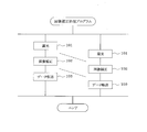
- FIG. 1 is a block diagram showing an image correction processing apparatus according to an embodiment of the present invention.
- FIG. 2 is a flowchart showing a flow of image correction processing when exposure is performed by a rolling shutter system.
- the camera unit 12 incorporating the image pickup device 11 is replaceably attached to an industrial machine such as a component mounter.
- the camera unit 12 is provided with a non-volatile memory 13 such as a flash memory, ROM, PROM, EPROM, or EEPROM, which is a non-volatile storage means.
- the nonvolatile memory 13 stores one or more image correction parameters among image distortion correction parameters, shading correction parameters, contrast correction parameters, pixel defect correction parameters, and the like.
- the image processing device 14 of an industrial machine such as a component mounter includes an FPGA (Field Programmable Gate Array) 15 that is a programmable logic device, a frame buffer, and the like.
- An image processing circuit 16 including the image processing circuit 16 is provided.
- the nonvolatile memory 13 in which the image correction parameters are stored is provided in the camera unit 12, but this may be provided in the image processing device 14.
- the FPGA 15 includes a plurality of line buffers 17 that sequentially read out pixel data for each scanning line of the image sensor 11 and temporarily store pixel data for a plurality of lines, a pixel data correction processing unit 18 (pixel data correction unit), and the like. Is provided.
- the pixel data correction processing unit 18 sets an intermediate line (n) of the pixel data for a plurality of lines stored in the plurality of line buffers 17 as a correction target line, and is adjacent to both upper and lower sides of the correction target line (n).
- the data is corrected, and the corrected pixel data is transferred to the image processing circuit 16.
- the nonvolatile memory 13 when correcting image distortion, it is stored in advance in the nonvolatile memory 13 as a distortion correction amount table in which the relationship between the distortion correction amount, which is an image distortion correction parameter, and pixel coordinates is set, and a pixel data correction processing unit 18, an interpolation correction method is applied to each pixel data of the correction target line (n) using a plurality of pixel data around each pixel of the correction target line (n) and the distortion correction amount retrieved from the distortion correction amount table. Therefore, the distortion may be corrected.
- the interpolation correction method for example, any one of bilinear interpolation, bicubic interpolation, nearest neighbor interpolation, and the like may be used.
- the FPGA 15 shifts the scanning line to store the pixel data of the plurality of lines (n ⁇ 3) to (n + 3) including the next correction target line in the plurality of line buffers 17 and corrects the pixel data by the pixel data correction processing unit 18.
- the pixel data of each line for one frame of the image sensor 11 is sequentially corrected and the image The data is sequentially transferred to the processing circuit 16.
- the FPGA 15 is provided with a buffer (memory) that temporarily stores the corrected pixel data transferred from the pixel data correction processing unit 18 for a predetermined number of lines, and the buffer is provided with a corrected number of lines after the correction. Each time pixel data is stored, corrected pixel data for a predetermined number of lines may be transferred from the buffer to the image processing circuit 16. In this way, high-speed correction processing can be performed while reducing the number of interruptions to the main CPU of the image processing apparatus 14.
- the electronic shutter of the image sensor 11 may be a rolling shutter that sequentially releases the shutter for each scanning line, or a global shutter that simultaneously releases the shutter for one frame.
- FIG. 2 is a flowchart showing the flow of image correction processing when exposure is performed by the rolling shutter method.
- the exposure is performed by sequentially releasing the shutter for each scanning line by the rolling shutter method, and the pixel data of the scanning line is stored in, for example, the line buffer 17 of the first column (step 101), and the line of the first column at the previous processing is stored.
- the pixel data of the line stored in the buffer 17 is shifted to the line buffer 17 in the second column.
- the pixel data of the line stored in the line buffer 17 in the “N” column during the previous processing is shifted to the line buffer 17 in the “N + 1” column.
- the pixel data of the line stored in the line buffer 17 in the last column at the previous processing is discarded.
- a total of six lines (n ⁇ 3), (n-3) adjacent to the upper and lower sides of the correction target line (n) stored in the intermediate line buffer 17 ( n-2), (n-1), (n + 1), (n + 2), and (n + 3) are used to correct the pixel data of the correction target line (n) by interpolation correction (step 102).
- the corrected pixel data is transferred to the image processing circuit 16 (step 103).
- the pixel data of each line for one frame of the image sensor 11 is sequentially corrected and sequentially transferred to the image processing circuit 16.
- the exposure need only be performed once at the beginning.
- the memory necessary for the image correction processing is stored. The amount can be greatly reduced, the circuit scale of the memory can be reduced, and the cost can be reduced.
- the processing for storing the pixel data for a plurality of lines in the plurality of line buffers 17 and the processing for correcting the pixel data of the correction target line can be performed in parallel, the time required for the image correction processing can be shortened, and image correction The processing speed can be increased.
- the number of line buffers 17 is not limited to 7 columns, and may be 3 columns, 5 columns, and the like. Further, a plurality of correction target lines may be set to correct pixel data of a plurality of correction target lines.
- the present invention is not limited to industrial machines such as component mounting machines, machine tools, printing machines, and inspection machines, and can be applied to various apparatuses equipped with an image processing function for processing an image captured by an image sensor.
- industrial machines such as component mounting machines, machine tools, printing machines, and inspection machines
- image processing function for processing an image captured by an image sensor.
Landscapes
- Engineering & Computer Science (AREA)
- Multimedia (AREA)
- Signal Processing (AREA)
- Image Processing (AREA)
- Studio Devices (AREA)
Abstract
FPGA15には、撮像素子11の走査ラインの画素データを順次読み出して複数ライン分の画素データを一時的に記憶する複数のラインバッファ17と、画素データ補正処理部18とが設けられている。画素データ補正処理部18は、複数のラインバッファ17に記憶された複数ライン分の画素データのうちの中間のライン(n)を補正対象ラインとし、該補正対象ライン(n)に隣接するラインの画素データを用いて該補正対象ライン(n)の画素データを補正して、補正後の画素データを画像処理回路16へ転送する。このような処理を走査ラインを1ラインずつシフトさせて繰り返すことで、撮像素子11の1フレーム分の各ラインの画素データを順次補正して該画像処理回路16へ順次転送する。
Description
本発明は、撮像素子の1フレーム分(1画面分)の画素データを補正する画像補正処理装置に関する発明である。
従来より、撮像素子で撮像する画像の品質を向上させるために、画像歪み補正、シェーディング補正、画素欠陥補正等の様々な画像補正機能を搭載した画像処理装置が実用化されている。特に、部品実装機に搭載した画像処理装置では、精密な位置決め精度が要求されるため、画像の歪みが大きな問題となる。従来の画像歪み補正技術は、予め、ドットマークが所定ピッチでマトリックス状に表示された画像歪み補正治具を撮像素子で撮像してドットマーク毎に歪み量を測定して歪み量のテーブルデータを作成して記憶しておき、撮像素子の1フレーム分の画素データを全てフレームバッファに記憶し終えてから、歪み量のテーブルデータを用いて画像の歪みを補正するようにしている(特許文献1,2参照)。
しかし、上記従来の構成では、撮像素子の1フレーム分の画素データを全てフレームバッファに記憶し終えてから、画像補正処理を行うようにしているため、画素データを記憶するバッファの回路規模が大きくなり、コスト高になると共に、画像補正処理の高速化にも限界がある。
そこで、本発明が解決しようとする課題は、低コスト化と画像補正処理の高速化を実現できる画像補正処理装置を提供することである。
上記課題を解決するために、本発明は、撮像対象物を撮像する撮像素子と、前記撮像素子の走査ライン毎に画素データを順次読み出して複数ライン分の画素データを一時的に記憶する複数のラインバッファと、前記複数のラインバッファに記憶された複数ライン分の画素データのうちの所定のラインを補正対象ラインとし、該補正対象ラインに隣接する少なくとも1つのラインの画素データを用いて該補正対象ラインの画素データを補正して、補正後の画素データを画像処理回路へ転送する画素データ補正手段とを備え、走査ラインをシフトさせて次の補正対象ラインを含む複数ライン分の画素データを前記複数のラインバッファに記憶する処理と、前記画素データ補正手段により前記補正対象ラインの画素データを補正して前記画像処理回路へ転送する処理とを繰り返すことで前記撮像素子の1フレーム分の各ラインの画素データを順次補正して該画像処理回路へ順次転送するようにしたものである。
この構成では、補正対象ラインの画素データを補正するのに必要な複数ライン分の画素データを複数のラインバッファに記憶するだけであるため、画像補正処理に必要なメモリ量を大幅に削減でき、メモリの回路規模を小さくできて、低コスト化を実現できる。しかも、複数ライン分の画素データを複数のラインバッファに記憶する処理と、補正対象ライ
ンの画素データを補正する処理とを並列処理できるため、画像補正処理に要する時間を短縮できて、画像補正処理の高速化を実現できる。
ンの画素データを補正する処理とを並列処理できるため、画像補正処理に要する時間を短縮できて、画像補正処理の高速化を実現できる。
更に、画像歪みを補正する場合は、歪み補正量と画素座標との関係を設定した歪み補正量テーブルを記憶手段に記憶しておき、画素データ補正手段において、補正対象ラインの各画素の周辺の複数の画素データと前記歪み補正量テーブルから検索した歪み補正量とを用いて該補正対象ラインの各画素データを補間補正法により歪み補正するようにすれば良い。これにより、画像歪みを補正する処理を高速化できる。
本発明の画像補正処理装置は、撮像素子で撮像した画像を処理する画像処理機能を搭載した様々な装置に適用でき、例えば、部品実装機等の産業用機械に適用すれば、部品実装機等の産業用機械の画像処理機能の低コスト化と高速処理化とを両立させることができる。
以下、本発明を実施するための形態を部品実装機、工作機、印刷機、検査機等の産業用機械の画像処理装置に適用して具体化した一実施例を図面を用いて説明する。
図1に示すように、撮像素子11を内蔵したカメラユニット12は、部品実装機等の産業用機械に交換可能に取り付けられる。このカメラユニット12には、不揮発性の記憶手段であるフラッシュメモリ、ROM、PROM、EPROM、EEPROM等の不揮発性メモリ13が取り付けられている。この不揮発性メモリ13には、画像歪み補正パラメータ、シェーディング補正パラメータ、コントラスト補正パラメータ、画素欠陥補正パラメータ等のうちの1つ以上の画像補正パラメータが記憶されている。
一方、部品実装機等の産業用機械の画像処理装置14には、メインCPU(図示せず)の他に、プログラム可能なロジックデバイスであるFPGA(Field Programmable Gate Array )15と、フレームバッファ等を含む画像処理回路16等が設けられている。尚、図1の構成例では、画像補正パラメータが記憶された不揮発性メモリ13をカメラユニット12に設けたが、これを画像処理装置14に設けた構成としても良い。
FPGA15には、撮像素子11の走査ライン毎に画素データを順次読み出して複数ライン分の画素データを一時的に記憶する複数のラインバッファ17と、画素データ補正処理部18(画素データ補正手段)とが設けられている。画素データ補正処理部18は、複数のラインバッファ17に記憶された複数ライン分の画素データのうちの中間のライン(n)を補正対象ラインとし、該補正対象ライン(n)の上下両側に隣接する合計6本のライン(n-3),(n-2),(n-1),(n+1),(n+2),(n+3)の画素データを用いて該補正対象ライン(n)の画素データを補正して、補正後の画素データを画像処理回路16へ転送する。
例えば、画像歪みを補正する場合は、予め、画像歪み補正パラメータである歪み補正量と画素座標との関係を設定した歪み補正量テーブルとして不揮発性メモリ13に記憶しておき、画素データ補正処理部18において、補正対象ライン(n)の各画素の周辺の複数
の画素データと前記歪み補正量テーブルから検索した歪み補正量とを用いて該補正対象ライン(n)の各画素データを補間補正法により歪み補正すれば良い。補間補正法としては、例えば、バイリニア補間、バイキュービック補間、最近傍補間等のいずれかを用いれば良い。
の画素データと前記歪み補正量テーブルから検索した歪み補正量とを用いて該補正対象ライン(n)の各画素データを補間補正法により歪み補正すれば良い。補間補正法としては、例えば、バイリニア補間、バイキュービック補間、最近傍補間等のいずれかを用いれば良い。
FPGA15は、走査ラインをシフトさせて次の補正対象ラインを含む複数ライン(n-3)~(n+3)の画素データを複数のラインバッファ17に記憶する処理と、画素データ補正処理部18により補正対象ライン(n)の画素データを補間補正法により補正して画像処理回路16へ転送する処理とを繰り返すことで、撮像素子11の1フレーム分の各ラインの画素データを順次補正して該画像処理回路16へ順次転送する。
尚、FPGA15に、画素データ補正処理部18から転送される補正後の画素データを所定ライン数分だけ一時的に記憶するバッファ(メモリ)を設けて、該バッファに所定ライン数分の補正後の画素データを記憶し終える毎に、該バッファから所定ライン数分の補正後の画素データを画像処理回路16へ転送するようにしても良い。このようにすれば、画像処理装置14のメインCPUへの割り込み回数を削減しつつ高速な補正処理を行うことができる。
撮像素子11の電子シャッタは、走査ライン毎に順次シャッタを切るローリングシャッタを用いても良いし、1フレーム同時にシャッタを切るグローバルシャッタを用いても良い。
図2は、ローリングシャッタ方式で露光する場合の画像補正処理の流れを示すフローチャートである。ローリングシャッタ方式で走査ライン毎に順次シャッタを切って露光して、該走査ラインの画素データを、例えば、1列目のラインバッファ17に記憶し(ステップ101)、前回処理時に1列目のラインバッファ17に記憶されていたラインの画素データを2列目のラインバッファ17にシフトさせる。前回処理時に「N」列目のラインバッファ17に記憶されていたラインの画素データは、「N+1」列目のラインバッファ17にシフトされる。前回処理時に最終列のラインバッファ17に記憶されていたラインの画素データは、廃棄される。
走査ラインの画素データを1列目のラインバッファ17に取り込む毎に、中間のラインバッファ17に記憶された補正対象ライン(n)の上下両側に隣接する合計6つのライン(n-3),(n-2),(n-1),(n+1),(n+2),(n+3)の画素データを用いて該補正対象ライン(n)の画素データを補間補正により補正して(ステップ102)、補正後の画素データを画像処理回路16へ転送する(ステップ103)。
以上の処理を走査ラインを1ラインずつシフトさせて繰り返すことで、撮像素子11の1フレーム分の各ラインの画素データを順次補正して該画像処理回路16へ順次転送する。
尚、グローバルシャッタ方式で露光する場合は、露光は最初に1回行うだけで良い。
以上説明した本実施例によれば、補正対象ラインの画素データを補正するのに必要な複数ライン分の画素データを複数のラインバッファ17に記憶するだけであるため、画像補正処理に必要なメモリ量を大幅に削減でき、メモリの回路規模を小さくできて、低コスト化を実現できる。しかも、複数ライン分の画素データを複数のラインバッファ17に記憶する処理と、補正対象ラインの画素データを補正する処理とを並列処理できるため、画像補正処理に要する時間を短縮できて、画像補正処理の高速化を実現できる。
以上説明した本実施例によれば、補正対象ラインの画素データを補正するのに必要な複数ライン分の画素データを複数のラインバッファ17に記憶するだけであるため、画像補正処理に必要なメモリ量を大幅に削減でき、メモリの回路規模を小さくできて、低コスト化を実現できる。しかも、複数ライン分の画素データを複数のラインバッファ17に記憶する処理と、補正対象ラインの画素データを補正する処理とを並列処理できるため、画像補正処理に要する時間を短縮できて、画像補正処理の高速化を実現できる。
尚、ラインバッファ17の数は7列に限定されず、例えば3列、5列等であっても良い
。また、補正対象ラインを複数設定して、複数の補正対象ラインの画素データを補正するようにしても良い。
。また、補正対象ラインを複数設定して、複数の補正対象ラインの画素データを補正するようにしても良い。
その他、本発明は、部品実装機、工作機、印刷機、検査機等の産業用機械に限定されず、撮像素子で撮像した画像を処理する画像処理機能を搭載した様々な装置に適用できる等、要旨を逸脱しない範囲内で種々変更して実施できる。
11…撮像素子、12…カメラユニット、13…不揮発性メモリ(記憶手段)、14…画像処理装置、15…FPGA、16…画像処理回路、17…ラインバッファ、18…画素データ補正処理部(画素データ補正手段)
Claims (3)
- 撮像対象物を撮像する撮像素子と、
前記撮像素子の走査ライン毎に画素データを順次読み出して複数ライン分の画素データを一時的に記憶する複数のラインバッファと、
前記複数のラインバッファに記憶された複数ライン分の画素データのうちの所定のラインを補正対象ラインとし、該補正対象ラインに隣接する少なくとも1つのラインの画素データを用いて該補正対象ラインの画素データを補正して、補正後の画素データを画像処理回路へ転送する画素データ補正手段とを備え、
走査ラインをシフトさせて次の補正対象ラインを含む複数ライン分の画素データを前記複数のラインバッファに記憶する処理と、前記画素データ補正手段により前記補正対象ラインの画素データを補正して前記画像処理回路へ転送する処理とを繰り返すことで前記撮像素子の1フレーム分の各ラインの画素データを順次補正して該画像処理回路へ順次転送することを特徴とする画像補正処理装置。 - 画像歪みを補正するための歪み補正量と画素座標との関係を設定した歪み補正量テーブルを記憶した記憶手段を備え、
前記画素データ補正手段は、前記補正対象ラインの各画素の周辺の複数の画素データと
前記歪み補正量テーブルから検索した歪み補正量とを用いて該補正対象ラインの各画素データを補間補正法により歪み補正することを特徴とする請求項1に記載の画像補正処理装置。 - 前記撮像素子は、部品実装機に搭載されていることを特徴とする請求項1に記載の画像補正処理装置。
Priority Applications (2)
| Application Number | Priority Date | Filing Date | Title |
|---|---|---|---|
| PCT/JP2012/056497 WO2013136458A1 (ja) | 2012-03-14 | 2012-03-14 | 画像補正処理装置 |
| JP2014504548A JP6146819B2 (ja) | 2012-03-14 | 2012-03-14 | 画像補正処理装置 |
Applications Claiming Priority (1)
| Application Number | Priority Date | Filing Date | Title |
|---|---|---|---|
| PCT/JP2012/056497 WO2013136458A1 (ja) | 2012-03-14 | 2012-03-14 | 画像補正処理装置 |
Publications (1)
| Publication Number | Publication Date |
|---|---|
| WO2013136458A1 true WO2013136458A1 (ja) | 2013-09-19 |
Family
ID=49160427
Family Applications (1)
| Application Number | Title | Priority Date | Filing Date |
|---|---|---|---|
| PCT/JP2012/056497 Ceased WO2013136458A1 (ja) | 2012-03-14 | 2012-03-14 | 画像補正処理装置 |
Country Status (2)
| Country | Link |
|---|---|
| JP (1) | JP6146819B2 (ja) |
| WO (1) | WO2013136458A1 (ja) |
Cited By (3)
| Publication number | Priority date | Publication date | Assignee | Title |
|---|---|---|---|---|
| JP2021060590A (ja) * | 2015-05-04 | 2021-04-15 | グーグル エルエルシーGoogle LLC | 取込まれた像のパススルー表示 |
| US11076092B2 (en) | 2018-09-18 | 2021-07-27 | Kabushiki Kaisha Toshiba | Image processing apparatus, image processing method, and image processing program |
| CN117274068A (zh) * | 2022-06-13 | 2023-12-22 | 深圳市普渡科技有限公司 | 图像的校正方法、系统和终端和计算机存储介质 |
Citations (4)
| Publication number | Priority date | Publication date | Assignee | Title |
|---|---|---|---|---|
| JPH11154228A (ja) * | 1997-11-25 | 1999-06-08 | Fuji Xerox Co Ltd | 画像処理装置および方法 |
| JP2001101396A (ja) * | 1999-09-30 | 2001-04-13 | Toshiba Corp | 画像歪み補正処理装置および方法、並びに画像歪み補正処理を行うプログラムを格納した媒体 |
| JP2005044098A (ja) * | 2003-07-28 | 2005-02-17 | Olympus Corp | 画像処理装置及び画像処理方法 |
| JP2011180084A (ja) * | 2010-03-03 | 2011-09-15 | Fuji Mach Mfg Co Ltd | 部品実装機の撮像画像処理装置 |
Family Cites Families (5)
| Publication number | Priority date | Publication date | Assignee | Title |
|---|---|---|---|---|
| JPH11154288A (ja) * | 1997-11-19 | 1999-06-08 | Matsushita Electric Works Ltd | 火災感知器及び火災感知器の取付方法 |
| JP3986877B2 (ja) * | 2002-04-26 | 2007-10-03 | 株式会社リコー | 画像処理装置 |
| JP3897247B2 (ja) * | 2002-05-16 | 2007-03-22 | 富士フイルム株式会社 | 光学歪みの補正方法及び補正装置 |
| JP4919836B2 (ja) * | 2006-03-01 | 2012-04-18 | パナソニック株式会社 | 画像の歪曲補正を行う画像処理装置、撮像装置及び画像の歪曲補正方法 |
| JP5299383B2 (ja) * | 2010-08-20 | 2013-09-25 | 株式会社Jvcケンウッド | 画像補正装置および画像補正方法 |
-
2012
- 2012-03-14 WO PCT/JP2012/056497 patent/WO2013136458A1/ja not_active Ceased
- 2012-03-14 JP JP2014504548A patent/JP6146819B2/ja active Active
Patent Citations (4)
| Publication number | Priority date | Publication date | Assignee | Title |
|---|---|---|---|---|
| JPH11154228A (ja) * | 1997-11-25 | 1999-06-08 | Fuji Xerox Co Ltd | 画像処理装置および方法 |
| JP2001101396A (ja) * | 1999-09-30 | 2001-04-13 | Toshiba Corp | 画像歪み補正処理装置および方法、並びに画像歪み補正処理を行うプログラムを格納した媒体 |
| JP2005044098A (ja) * | 2003-07-28 | 2005-02-17 | Olympus Corp | 画像処理装置及び画像処理方法 |
| JP2011180084A (ja) * | 2010-03-03 | 2011-09-15 | Fuji Mach Mfg Co Ltd | 部品実装機の撮像画像処理装置 |
Cited By (3)
| Publication number | Priority date | Publication date | Assignee | Title |
|---|---|---|---|---|
| JP2021060590A (ja) * | 2015-05-04 | 2021-04-15 | グーグル エルエルシーGoogle LLC | 取込まれた像のパススルー表示 |
| US11076092B2 (en) | 2018-09-18 | 2021-07-27 | Kabushiki Kaisha Toshiba | Image processing apparatus, image processing method, and image processing program |
| CN117274068A (zh) * | 2022-06-13 | 2023-12-22 | 深圳市普渡科技有限公司 | 图像的校正方法、系统和终端和计算机存储介质 |
Also Published As
| Publication number | Publication date |
|---|---|
| JPWO2013136458A1 (ja) | 2015-08-03 |
| JP6146819B2 (ja) | 2017-06-14 |
Similar Documents
| Publication | Publication Date | Title |
|---|---|---|
| TWI569643B (zh) | 用於提供延伸視野影像的攝像系統及方法 | |
| JP6141084B2 (ja) | 撮像装置 | |
| US9413997B2 (en) | Method and device for processing captured-image signals | |
| EP2068280A3 (en) | Image processing apparatus, image processing method, image processing program and position detecting apparatus as well as mobile object having the same | |
| JP2012054755A (ja) | 高速度ビデオカメラ | |
| JP6146819B2 (ja) | 画像補正処理装置 | |
| US7990581B2 (en) | Image processing apparatus, control method for controlling the image processing apparatus, and computer-readable storage medium | |
| JP5398750B2 (ja) | カメラモジュール | |
| JP5121870B2 (ja) | 画像処理方法および画像処理装置 | |
| US20120242784A1 (en) | Image processing method, camera module, and photographing method | |
| JP2017138288A (ja) | 画像測定機及びプログラム | |
| CN113824935A (zh) | 伪彩色线扫描相机的时间延迟积分方法、装置及设备 | |
| JP2009510868A (ja) | 製造過程におけるカメラ特性の内部記憶装置 | |
| JP2006058945A (ja) | ローリングシャッタ画像の補正方法および装置 | |
| JP5676233B2 (ja) | 画像処理装置、画像処理方法、及び撮像装置 | |
| JP4521858B2 (ja) | 画像処理装置 | |
| US8730370B2 (en) | Solid-state imaging device having image pixel position correction to reduce shape distortion | |
| JP2010212788A (ja) | 撮像装置、欠陥画素補正方法、および電子情報機器 | |
| JP4771901B2 (ja) | 撮像装置、画像歪み補正方法及びプログラム | |
| JP2005210164A5 (ja) | ||
| JP2009194424A (ja) | ラインセンサ装置 | |
| JP2014033415A (ja) | 画像処理装置及び方法、及び、撮像装置 | |
| JP2014099714A (ja) | 画像処理装置、撮像装置、画像処理方法及びプログラム | |
| JP6648985B2 (ja) | 画像処理装置および画像処理方法 | |
| JP2012216947A5 (ja) | 撮像装置、画像処理方法及び画像処理装置 |
Legal Events
| Date | Code | Title | Description |
|---|---|---|---|
| 121 | Ep: the epo has been informed by wipo that ep was designated in this application |
Ref document number: 12871019 Country of ref document: EP Kind code of ref document: A1 |
|
| ENP | Entry into the national phase |
Ref document number: 2014504548 Country of ref document: JP Kind code of ref document: A |
|
| NENP | Non-entry into the national phase |
Ref country code: DE |
|
| 122 | Ep: pct application non-entry in european phase |
Ref document number: 12871019 Country of ref document: EP Kind code of ref document: A1 |