WO2013133251A1 - Surface coating cutting tool - Google Patents
Surface coating cutting tool Download PDFInfo
- Publication number
- WO2013133251A1 WO2013133251A1 PCT/JP2013/055924 JP2013055924W WO2013133251A1 WO 2013133251 A1 WO2013133251 A1 WO 2013133251A1 JP 2013055924 W JP2013055924 W JP 2013055924W WO 2013133251 A1 WO2013133251 A1 WO 2013133251A1
- Authority
- WO
- WIPO (PCT)
- Prior art keywords
- coating layer
- hard coating
- tool
- grain size
- flank
- Prior art date
Links
Images

Classifications
-
- C—CHEMISTRY; METALLURGY
- C23—COATING METALLIC MATERIAL; COATING MATERIAL WITH METALLIC MATERIAL; CHEMICAL SURFACE TREATMENT; DIFFUSION TREATMENT OF METALLIC MATERIAL; COATING BY VACUUM EVAPORATION, BY SPUTTERING, BY ION IMPLANTATION OR BY CHEMICAL VAPOUR DEPOSITION, IN GENERAL; INHIBITING CORROSION OF METALLIC MATERIAL OR INCRUSTATION IN GENERAL
- C23C—COATING METALLIC MATERIAL; COATING MATERIAL WITH METALLIC MATERIAL; SURFACE TREATMENT OF METALLIC MATERIAL BY DIFFUSION INTO THE SURFACE, BY CHEMICAL CONVERSION OR SUBSTITUTION; COATING BY VACUUM EVAPORATION, BY SPUTTERING, BY ION IMPLANTATION OR BY CHEMICAL VAPOUR DEPOSITION, IN GENERAL
- C23C14/00—Coating by vacuum evaporation, by sputtering or by ion implantation of the coating forming material
- C23C14/06—Coating by vacuum evaporation, by sputtering or by ion implantation of the coating forming material characterised by the coating material
- C23C14/0641—Nitrides
-
- B—PERFORMING OPERATIONS; TRANSPORTING
- B23—MACHINE TOOLS; METAL-WORKING NOT OTHERWISE PROVIDED FOR
- B23B—TURNING; BORING
- B23B27/00—Tools for turning or boring machines; Tools of a similar kind in general; Accessories therefor
- B23B27/14—Cutting tools of which the bits or tips or cutting inserts are of special material
-
- B—PERFORMING OPERATIONS; TRANSPORTING
- B23—MACHINE TOOLS; METAL-WORKING NOT OTHERWISE PROVIDED FOR
- B23B—TURNING; BORING
- B23B51/00—Tools for drilling machines
-
- B—PERFORMING OPERATIONS; TRANSPORTING
- B23—MACHINE TOOLS; METAL-WORKING NOT OTHERWISE PROVIDED FOR
- B23C—MILLING
- B23C5/00—Milling-cutters
- B23C5/16—Milling-cutters characterised by physical features other than shape
-
- C—CHEMISTRY; METALLURGY
- C23—COATING METALLIC MATERIAL; COATING MATERIAL WITH METALLIC MATERIAL; CHEMICAL SURFACE TREATMENT; DIFFUSION TREATMENT OF METALLIC MATERIAL; COATING BY VACUUM EVAPORATION, BY SPUTTERING, BY ION IMPLANTATION OR BY CHEMICAL VAPOUR DEPOSITION, IN GENERAL; INHIBITING CORROSION OF METALLIC MATERIAL OR INCRUSTATION IN GENERAL
- C23C—COATING METALLIC MATERIAL; COATING MATERIAL WITH METALLIC MATERIAL; SURFACE TREATMENT OF METALLIC MATERIAL BY DIFFUSION INTO THE SURFACE, BY CHEMICAL CONVERSION OR SUBSTITUTION; COATING BY VACUUM EVAPORATION, BY SPUTTERING, BY ION IMPLANTATION OR BY CHEMICAL VAPOUR DEPOSITION, IN GENERAL
- C23C14/00—Coating by vacuum evaporation, by sputtering or by ion implantation of the coating forming material
- C23C14/06—Coating by vacuum evaporation, by sputtering or by ion implantation of the coating forming material characterised by the coating material
- C23C14/14—Metallic material, boron or silicon
-
- C—CHEMISTRY; METALLURGY
- C23—COATING METALLIC MATERIAL; COATING MATERIAL WITH METALLIC MATERIAL; CHEMICAL SURFACE TREATMENT; DIFFUSION TREATMENT OF METALLIC MATERIAL; COATING BY VACUUM EVAPORATION, BY SPUTTERING, BY ION IMPLANTATION OR BY CHEMICAL VAPOUR DEPOSITION, IN GENERAL; INHIBITING CORROSION OF METALLIC MATERIAL OR INCRUSTATION IN GENERAL
- C23C—COATING METALLIC MATERIAL; COATING MATERIAL WITH METALLIC MATERIAL; SURFACE TREATMENT OF METALLIC MATERIAL BY DIFFUSION INTO THE SURFACE, BY CHEMICAL CONVERSION OR SUBSTITUTION; COATING BY VACUUM EVAPORATION, BY SPUTTERING, BY ION IMPLANTATION OR BY CHEMICAL VAPOUR DEPOSITION, IN GENERAL
- C23C14/00—Coating by vacuum evaporation, by sputtering or by ion implantation of the coating forming material
- C23C14/22—Coating by vacuum evaporation, by sputtering or by ion implantation of the coating forming material characterised by the process of coating
- C23C14/24—Vacuum evaporation
- C23C14/32—Vacuum evaporation by explosion; by evaporation and subsequent ionisation of the vapours, e.g. ion-plating
- C23C14/325—Electric arc evaporation
-
- C—CHEMISTRY; METALLURGY
- C23—COATING METALLIC MATERIAL; COATING MATERIAL WITH METALLIC MATERIAL; CHEMICAL SURFACE TREATMENT; DIFFUSION TREATMENT OF METALLIC MATERIAL; COATING BY VACUUM EVAPORATION, BY SPUTTERING, BY ION IMPLANTATION OR BY CHEMICAL VAPOUR DEPOSITION, IN GENERAL; INHIBITING CORROSION OF METALLIC MATERIAL OR INCRUSTATION IN GENERAL
- C23C—COATING METALLIC MATERIAL; COATING MATERIAL WITH METALLIC MATERIAL; SURFACE TREATMENT OF METALLIC MATERIAL BY DIFFUSION INTO THE SURFACE, BY CHEMICAL CONVERSION OR SUBSTITUTION; COATING BY VACUUM EVAPORATION, BY SPUTTERING, BY ION IMPLANTATION OR BY CHEMICAL VAPOUR DEPOSITION, IN GENERAL
- C23C14/00—Coating by vacuum evaporation, by sputtering or by ion implantation of the coating forming material
- C23C14/22—Coating by vacuum evaporation, by sputtering or by ion implantation of the coating forming material characterised by the process of coating
- C23C14/50—Substrate holders
- C23C14/505—Substrate holders for rotation of the substrates
-
- B—PERFORMING OPERATIONS; TRANSPORTING
- B23—MACHINE TOOLS; METAL-WORKING NOT OTHERWISE PROVIDED FOR
- B23B—TURNING; BORING
- B23B2222/00—Materials of tools or workpieces composed of metals, alloys or metal matrices
- B23B2222/28—Details of hard metal, i.e. cemented carbide
-
- B—PERFORMING OPERATIONS; TRANSPORTING
- B23—MACHINE TOOLS; METAL-WORKING NOT OTHERWISE PROVIDED FOR
- B23B—TURNING; BORING
- B23B2224/00—Materials of tools or workpieces composed of a compound including a metal
-
- B—PERFORMING OPERATIONS; TRANSPORTING
- B23—MACHINE TOOLS; METAL-WORKING NOT OTHERWISE PROVIDED FOR
- B23C—MILLING
- B23C2222/00—Materials of tools or workpieces composed of metals, alloys or metal matrices
- B23C2222/28—Details of hard metal, i.e. cemented carbide
-
- B—PERFORMING OPERATIONS; TRANSPORTING
- B23—MACHINE TOOLS; METAL-WORKING NOT OTHERWISE PROVIDED FOR
- B23C—MILLING
- B23C2224/00—Materials of tools or workpieces composed of a compound including a metal
-
- Y—GENERAL TAGGING OF NEW TECHNOLOGICAL DEVELOPMENTS; GENERAL TAGGING OF CROSS-SECTIONAL TECHNOLOGIES SPANNING OVER SEVERAL SECTIONS OF THE IPC; TECHNICAL SUBJECTS COVERED BY FORMER USPC CROSS-REFERENCE ART COLLECTIONS [XRACs] AND DIGESTS
- Y10—TECHNICAL SUBJECTS COVERED BY FORMER USPC
- Y10T—TECHNICAL SUBJECTS COVERED BY FORMER US CLASSIFICATION
- Y10T407/00—Cutters, for shaping
- Y10T407/27—Cutters, for shaping comprising tool of specific chemical composition
Definitions
- the present invention relates to a surface-coated cutting tool (hereinafter referred to as a coated tool) that exhibits excellent chipping resistance and abrasion resistance in a cutting process such as carbon steel and alloy steel.
- a coated tool a surface-coated cutting tool
- This application claims priority based on Japanese Patent Application No. 2012-047926 filed in Japan on March 5, 2012 and Japanese Patent Application No. 2013-40331 filed in Japan on March 1, 2013. The contents are incorporated herein.
- throwaway inserts that are used to attach and detachably attach to the tip of a cutting tool for turning and planing of various steel and cast iron materials, drilling and cutting of the above-mentioned work material, etc.
- drills used in the above, solid type end mills used for chamfering, grooving, shoulder processing, etc. of the above work material, and the same as the above solid type end mills with the above throwaway tip attached detachably Slow-away end mill tools that perform cutting work are known.
- Patent Document 1 As a coated tool, a composite nitride of Al and Cr is formed on the surface of a base (hereinafter referred to as a tool base) made of tungsten carbide (hereinafter referred to as WC) based cemented carbide.
- a coating tool formed by vapor-depositing a hard coating layer composed of a layer [hereinafter referred to as (Al, Cr) N] is known.
- the above (Al, Since the Cr) N layer has excellent high-temperature hardness, heat resistance, high-temperature strength, high-temperature oxidation resistance, etc., it is known to exhibit excellent cutting performance.
- the conventional coated tool for example, as shown in FIGS.
- the tool base is loaded into an arc ion plating apparatus which is a kind of physical vapor deposition apparatus, and the tool base is set to 500 with a heater. While being heated to a temperature of 0 ° C., an arc discharge is generated between the anode electrode and the cathode electrode on which an Al—Cr alloy having a predetermined composition is set under the condition of current: 90 A, and at the same time, nitrogen as a reaction gas in the apparatus A gas is introduced to form a reaction atmosphere of 2 Pa.
- the (Al, Cr) N layer is deposited on the surface of the tool base under the condition that a bias voltage of ⁇ 100 V is applied to the tool base. It is also known that it can be manufactured.
- Patent Document 2 discloses that the coating layer is made of columnar crystals as a coating tool that improves chipping resistance by suppressing chipping of the coating layer on the rake face and improves wear resistance on the flank face.
- the coating layer thickness at the rake face is smaller than the coating layer thickness at the flank face, and the average crystal width of the upper layer region on the coating layer surface side is larger than the average crystal width of the lower layer region on the coating layer substrate side.
- the ratio of the thickness of the upper layer region to the coating layer thickness at the rake face is smaller than the ratio of the thickness of the upper layer region to the coating layer thickness at the flank face, and the average crystal width of the columnar crystals at the rake face Describes a coated tool (end mill) that is smaller than the average crystal width of the columnar crystals at the flank face.
- the film formed on the substrate is: A first coating layer, the first coating layer includes a microstructure region and a coarse tissue region, and the microstructure region has an average crystal grain size of a compound constituting it of 10 to 200 nm; and An average compressive stress that occupies a range of 50% or more of the total thickness of the first coating layer from the surface side of the first coating layer and is a stress in a range of ⁇ 4 GPa to ⁇ 2 GPa
- the first coating layer has a stress distribution in its thickness direction, and has two or more maximum values or minimum values in the stress distribution, and these maximum values or minimum values are the thickness direction surface. Coated tools with higher compressive stress are recorded on the side. It is.
- Japanese Patent No. 3969230 B
- Japanese Unexamined Patent Publication No. 2008-296290 A
- Japanese Unexamined Patent Publication No. 2011-67883 A
- the conventional coated tool can improve chipping resistance, chipping resistance, and wear resistance to some extent, but if it is used for more severe cutting such as carbon steel and alloy steel, chipping will not occur. It is easy to occur or wear and wear increase, and this causes the service life in a relatively short time.
- the present inventors are excellent in wear resistance as well as chipping resistance in cutting of carbon steel, alloy steel, etc., in order to provide a coated tool that exhibits excellent cutting performance over a long period of use.
- the following knowledge was obtained.
- a CVD method As a means for forming a hard coating layer, a CVD method, a PVD method, or the like is generally employed as a means for forming a coated tool.
- a PVD method an arc ion plating method (hereinafter referred to as a PVD method)
- the hard coating layer made of (Al, Cr) N is formed by the AIP method)
- the tool base is inserted into the apparatus and a predetermined bias voltage is applied.
- an arc discharge is generated between the anode electrode and an Al—Cr alloy target having a predetermined composition while the inside of the apparatus is heated to a predetermined temperature, and at the same time, nitrogen gas is introduced into the apparatus as a reactive gas, A hard coating layer was formed by vapor deposition in the reaction atmosphere (see FIGS. 1A and 1B).
- the inventors applied a magnetic field between the tool base and the target when forming the hard coating layer made of (Al, Cr) N by the conventional AIP method, and measured the influence of the magnetic field on the structure of the hard coating layer. I examined it. As a result, the following was found.
- the hard coating layer by the AIP method in a magnetic field having a predetermined strength, the crystal grain size of the granular crystal grains constituting the hard coating layer can be adjusted. Moreover, the value of the residual stress formed in the hard coating layer can be controlled. Furthermore, the crack occupation rate of the continuous crack formed in the corner part of a cutting-blade front-end
- the coated tool provided with the hard coating layer made of (Al, Cr) N in which the crystal grain size, the residual stress value and the crack occupancy of the hard coating layer are optimized in this way is carbon steel, alloy steel, etc. Excellent cutting resistance and wear resistance in cutting. As a result, this coated tool exhibits excellent cutting performance over a long period of use.
- the present invention has been made based on the above findings and has the following aspects.
- a surface-coated cutting tool in which a hard coating layer having an average layer thickness of 2 to 10 ⁇ m is vapor-deposited on the surface of a tool base composed of a tungsten carbide-based cemented carbide,
- the hard coating layer is composed of a composite nitride layer of Al and Cr, and the content ratio of Cr in the total amount of Al and Cr is 0.2 to 0.5 (however, the atomic ratio)
- the layer has a granular crystal structure, and the average grain size of the granular crystal grains on the surface of the hard coating layer formed on the region is 0.2 to 0.5 ⁇ m.
- the average grain size of the granular crystal grains at the interface of the coating layer is 0.02 to 0.1 ⁇ m smaller than the average grain size of the granular crystal grains on the surface of the hard coating layer, and the grain size is 0.15 ⁇ m or less.
- a surface-coated cutting tool wherein the crystal grain length ratio is 20% or less.
- the tool base is supported so that a part or all of the flank of the tool base and the surface of the target on the tool base side are horizontal when the tool base is manufactured.
- Method. (6) The method for producing a surface-coated cutting tool according to (5), wherein the magnetic field is 140 to 400 mT ⁇ mm as an integrated magnetic force.
- the coated tool according to one aspect of the present invention has a hard coating layer composed of an (Al, Cr) N layer having a predetermined composition in a range up to a position 100 ⁇ m away from the blade edge. Consisting of a granular crystal structure, the surface particle size is 0.2 to 0.5 ⁇ m, the interface particle size is 0.02 to 0.1 ⁇ m smaller than the surface particle size, and 100 ⁇ m from the cutting edge on the flank face In the range up to the distant position, the crystal grain length ratio occupied by crystal grains having a grain size of 0.15 ⁇ m or less is 20% or less, and the compressive residual stress in the hard coating layer is 2.0 to 2.7 GPa. Because the crack occupancy ratio ⁇ / ⁇ of the cutting edge is 0.3 to 1.0, it exhibits excellent chipping resistance and wear resistance in cutting of carbon steel, alloy steel, etc. Excellent cutting performance over use.
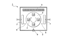
- the schematic explanatory drawing of the conventional AIP apparatus is shown, and the top view is shown.
- the schematic explanatory drawing of the conventional AIP apparatus is shown, and the side view is shown.
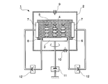
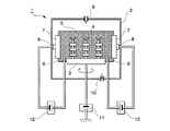
- the schematic explanatory drawing of the AIP apparatus for producing the covering tool of this invention is shown, (The top view is shown.
- the schematic explanatory drawing of the AIP apparatus for producing the covering tool of this invention is shown, and the side view is shown.
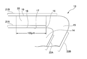
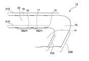
- the longitudinal cross-section schematic explanatory drawing of the coated tool of 1 aspect of this invention is shown.
- FIG. 3A is a schematic explanatory view of a longitudinal section of a coated tool of one embodiment of the present invention.
- a hard coating layer 15 is formed on a base 14.
- a cutting edge portion is formed between the flank 21 and the rake face 22 of the covering tool 13.
- the hard coating layer 15 of the coated tool 13 of the present invention is composed of a composite nitride layer ((Al, Cr) N layer) of Al and Cr.
- the Al component improves the high temperature hardness and heat resistance
- the Cr component improves the high temperature strength
- the high temperature oxidation resistance is improved by the coexistence of Cr and Al. It is already well known as a hard coating layer having excellent hardness, heat resistance, high temperature strength and high temperature oxidation resistance. If the content ratio of Cr in the total amount with Al (atomic ratio, the same applies hereinafter) is less than 0.2, it is difficult to ensure high temperature strength at the time of cutting, while Cr accounts for the total amount with Al. When the content ratio (atomic ratio) exceeds 0.5, the Al content ratio is relatively reduced, leading to a decrease in high-temperature hardness and a decrease in heat resistance.
- the Cr content (atomic ratio) in the total amount with Al is 0.2 to 0.5.
- a more preferable Cr content is 0.22 to 0.45.
- An even more preferable Cr content is 0.25 to 0.42.
- the average thickness of the hard coating layer made of the (Al, Cr) N layer is less than 2 ⁇ m, excellent wear resistance cannot be exhibited over a long period of time, resulting in a short tool life.
- the average layer thickness exceeds 10 ⁇ m, chipping tends to occur at the blade edge portion.
- the average layer thickness of the hard coating layer 15 in the coated tool 13 of the present invention is 2 to 10 ⁇ m.
- the average layer thickness of the hard coating layer 15 is more preferably 2.5-9.
- An even more preferred average layer thickness is 3-8.
- (B) Layer structure of hard coating layer composed of (Al, Cr) N layer In the coated tool 13 of the present invention, the compressive residual stress in the hard coating layer is reduced by forming a hard coating layer having more special properties in a specific region of the flank 21.
- the above flank specific area is a region 17 from the blade edge 16 on the flank surface to a position 100 ⁇ m away from the flank blade edge 16 toward the opposite side on the flank surface.
- the hard coating layer 20 formed on the region 17 has the characteristics described below.
- the hard coating layer 20 made of the (Al, Cr) N layer is formed as a granular crystal.
- the average crystal grain size (hereinafter simply referred to as “surface grain size”) of the crystal grains on the surface 19 of the hard coating layer 20 is set to 0.2 to 0.5 ⁇ m.
- the average crystal grain size of the hard coating layer 20 at the interface 18 between the tool base 14 and the hard coating layer 20 (hereinafter, simply referred to as “interface grain size”) is 0.02 to 0.
- the film is formed with a value 1 ⁇ m smaller. That is, on this region 17, the crystal structure of the hard coating layer 20 is formed such that the surface grain size and the interface grain size are in different average crystal grain size ranges. Thereby, it forms into a film so that the compression residual stress formed in a hard coating layer may become in a predetermined numerical range.
- the crystal grains of the hard coating layer at the interface between the tool base and the hard coating layer means the inside of the hard coating layer having a thickness of 0.5 ⁇ m from the interface between the tool base 14 and the hard coating layer 20 in the hard coating layer. It means crystal grains formed in the region.
- crystal grains on the surface of the hard coating layer means crystal grains formed in a region having a depth of 0.5 ⁇ m from the surface of the hard coating layer 20.
- the term “granular crystal” used herein is a term used to distinguish from “columnar crystal”, and specifically means that the aspect ratio of the crystal grain is 1 or more and 6 or less. . The aspect ratio is calculated as the ratio of the longest diameter (long side) to the diameter (short side) perpendicular to the crystal grain cross section, with the long side as the numerator and the short side as the denominator.
- the average crystal grain size will be specifically described as follows.
- the average crystal grain size (surface grain size) of the crystal grains on the hard coating layer surface 19 is less than 0.2 ⁇ m, the compressive residual stress in the hard coating layer increases, so that chipping is likely to occur during cutting.
- the surface particle diameter exceeds 0.5 ⁇ m, the compressive residual stress is reduced, so that the amount of wear during cutting increases, and sufficient wear resistance cannot be exhibited over a long period of use. From the above, the surface particle size of the hard coating layer 20 in the coated tool 13 of the present invention is determined to be 0.2 to 0.5 ⁇ m.
- the average crystal grain size (interface grain size) of the crystal grains of the hard coating layer 20 at the interface 18 between the tool base 14 and the hard coating layer 20 should be a value smaller by 0.02 to 0.1 ⁇ m than the surface grain size. is required.
- the technical reason is that when the interface particle size is smaller than 0.1 ⁇ m from the surface particle size, the difference between the surface particle size and the interface particle size becomes large, and the compressive residual stress in each part The difference increases and the entire film becomes brittle. Therefore, wear and chipping are likely to occur during cutting, resulting in a problem that the cutting performance deteriorates.
- the difference between the interface particle size and the surface particle size is within 0.02 ⁇ m, the difference in compressive residual stress between the surface and the interface becomes the same, and the effect of improving the wear resistance when cutting is performed. Because it cannot be granted.
- the interface particle size is set to a value smaller by 0.02 to 0.1 ⁇ m than the surface particle size, the compressive residual stress on the interface side is increased to such an extent that the entire film does not become brittle.
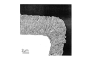
- the particle size measurement method is described below with reference to FIG. 3B. A section on the flank side is cut out from the tool base blade edge, and the section is observed with an SEM.
- a straight line is drawn parallel to the tool substrate surface, and the distance between crystal grain boundaries is defined as the grain size.
- the position where a straight line is drawn parallel to the surface of the tool base is the position where the longest crystal grain size is obtained in each crystal grain.
- the crystal grain size is measured in a region 17 from the cutting edge 16 on the flank to a position 100 ⁇ m away, and the average value of the average crystal grain size is defined as the surface grain size. More specifically, the edge 16 on the flank and the position on the flank at a position 50 ⁇ m away from the edge and 100 ⁇ m away from the edge within a range of 10 ⁇ m wide (in FIG.
- the interface grain size is calculated by the same method for each crystal grain formed in a region having a thickness of 0.5 ⁇ m from the interface 18 between the tool base 14 and the hard coating layer 20 in the hard coating layer.
- a region 17 up to a position 100 ⁇ m away from the cutting edge 16 on the flank (specifically, the blade edge on the flank and the position on the flank 50 ⁇ m away from the cutting edge and 100 ⁇ m away from the cutting edge)
- the crystal grain length ratio occupied by crystal grains having a grain size of 0.15 ⁇ m or less is required to be 20% or less for both the surface grain size and the interface grain size. This is because when the fine crystal grains having a grain size of 0.15 ⁇ m or less are formed in excess of 20%, the compressive residual stress in the hard coating layer is increased and chipping is likely to occur.
- the ratio of the crystal grain length occupied by crystal grains having a grain size of 0.15 ⁇ m or less means that the grain diameter of a plurality of crystal grains is measured, and the grain diameter is 0.15 ⁇ m relative to the sum of all the measured crystal grain lengths. The ratio of the sum of the following crystal grain lengths is shown.
- the “blade tip” is “the portion closest to the tip of the linear cutting blade excluding the conical portion of the corner portion at the tip of the cutting blade”. This is defined in the present invention.
- 3C is a longitudinal cross-sectional schematic explanatory diagram of the coated tool of one embodiment of the present invention, and is a diagram illustrating the positional relationship between the intersection of the virtual extension line of the base flank and the base rake face and the cutting edge on the flank. .
- FIG. 3C only the substrate is shown and the hard coating layer is not shown.
- the distance L ( ⁇ m) between the intersection 23 of the virtual extension line of the base flank 21 and the base rake face 22 and the cutting edge 16 on the flank has the following relationship.
- the (Al, Cr) N layer having the layer structure (b) is formed as the hard coating layer 20 on the region 17 so that the hard coating layer has a thickness of 2.0 to 2.7 GPa.
- compressive residual stress If the value of the compressive residual stress is less than 2.0 GPa, improvement in wear resistance cannot be expected. On the other hand, if this value exceeds 2.7 GPa, chipping is likely to occur.
- the value of the compressive residual stress in the hard coating layer is desirably set to 2.0 to 2.7 GPa.
- the cutting edge angle of the coated tool is ⁇ degrees, and continuous cracks formed in the hard coating layer within the angle range of the ⁇ degrees.
- the crack occupying ratio ⁇ / ⁇ at the corner portion at the tip of the cutting edge is preferably 0.3 to 1.0, and ⁇ / ⁇ is preferably 0.3 to 0.9. It is more preferable that The reason is as follows.
- the crack in this invention means the crack formed in the hard coating layer containing the corner part of a cutting-blade front-end
- the crack in the present invention means a crack having a width of 30 nm or more. The point where the width of the crack tapers at the end and the width of the crack is less than 30 nm is defined as the end of the crack.
- the crack occupation ratio is defined as follows in the present invention. As shown in FIGS.
- the value of (occupation angle ⁇ of continuous crack) / (blade edge angle ⁇ ) is defined as the crack occupancy rate.
- the average layer thickness of the hard coating layer composed of the (Al, Cr) N layer is 2 to 10 ⁇ m, and the content ratio of Cr in the total amount of Al and Cr is 0.2 to 0.5 ( However, the atomic ratio), the surface grain size of the granular crystal grains, and the interface grain size are set in specific numerical ranges, and the grain size in the region 17 up to a position 100 ⁇ m away from the cutting edge 16 on the flank is 0.15 ⁇ m or less.
- the value of the compressive residual stress in the hard coating layer is 2.0 to 2.7 GPa, and the crack occupation ratio ⁇ / ⁇ of the blade edge is A coated cutting tool having a thickness of 0.3 to 1 can be produced efficiently.
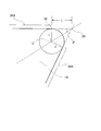
- the hard coating layer of the present invention uses an arc ion plating apparatus (AIP apparatus) as shown in FIGS. 2A and 2B, and maintains the temperature of the tool base at 370 to 450 ° C.
- AIP apparatus arc ion plating apparatus
- the tool base is rotated and revolved in the AIP apparatus, and is deposited by applying a predetermined magnetic field (integrated magnetic force 140 to 400 mT ⁇ mm) between the center of the target surface and the tool base closest to the target. can do.
- a cathode electrode made of a Ti electrode for substrate cleaning is provided on one side of the AIP apparatus, and a target (cathode electrode) made of an Al—Cr alloy is provided on the other side.
- the Al content in this Al—Cr alloy is preferably 55 at% Al to 78 at% Al.
- the Cr content is preferably 22 at% Cr to 45 at% Cr corresponding to the Al content.
- a target (cathode electrode) made of a 70 at% Al-30 at% Cr alloy is provided.
- a tool substrate made of tungsten carbide (WC) -based cemented carbide is cleaned and dried, mounted on a rotary table in an AIP apparatus, and 100 A between the Ti electrode and the anode electrode for cleaning the substrate in vacuum.
- An arc discharge is generated to bombard the surface of the tool base while applying a bias voltage of ⁇ 1000 V to the tool base.
- a magnetic field having an integrated magnetic force of 140 to 400 mT ⁇ mm from the center of the surface of the Al—Cr alloy target to the tool base closest to the target is applied.
- nitrogen gas is introduced into the apparatus as a reaction gas.
- the atmospheric pressure in the apparatus is maintained in the range of 9.0 Pa to 9.6 Pa.
- the atmospheric pressure is set to 9.3 Pa.
- a 100 A arc discharge is generated between the Al—Cr alloy target (cathode electrode) and the anode electrode.
- the hard coating layer can be formed by vapor deposition.
- the application of the magnetic field between the Al—Cr alloy target and the tool base is performed by, for example, installing an electromagnetic coil or permanent magnet as a magnetic field generation source around the cathode, or by permanent attachment in the center of the AIP device.
- the magnetic field can be formed by any means such as disposing a magnet.
- medium coarse WC powder having an average particle diameter of 5.5 ⁇ m, fine WC powder of 0.8 ⁇ m, TaC powder of 1.3 ⁇ m, NbC powder of 1.2 ⁇ m, ZrC of 1.2 ⁇ m Powder, 2.3 ⁇ m Cr 3 C 2 powder, 1.5 ⁇ m VC powder, 1.0 ⁇ m (Ti, W) C [by mass ratio, TiC / WC 50/50] powder, and 1 Co powder of 8 ⁇ m was prepared.
- Each of these raw material powders was blended in the blending composition shown in Table 5, further added with wax, mixed in a ball mill for 24 hours in acetone, and dried under reduced pressure.
- the diameter x length of the cutting edge portion is 6 mm x 13 mm, and it is made of a WC-based cemented carbide having a two-blade ball shape with a twist angle of 30 degrees.
- Tool bases (end mills) 1 to 3 and tool bases (end mills) 4 and 5 made of a WC-based cemented carbide having a two-blade square shape with a diameter ⁇ length of the cutting edge portion of 10 mm ⁇ 22 mm. Each was manufactured.
- Each of the tool bases 1 to 5 is ultrasonically cleaned in acetone and dried, and is separated from the central axis on the rotary table of the AIP apparatus shown in FIGS. 2A and 2B by a predetermined distance in the radial direction. Attached along the outer periphery at the position. A Ti cathode electrode for bombard cleaning was placed on one side of the AIP apparatus, and a target (cathode electrode) made of a 70 at% Al-30 at% Cr alloy was placed on the other side. (B) Next, the tool base is heated to 400 ° C. with a heater while the apparatus is evacuated and kept in vacuum, and then a DC bias voltage of ⁇ 1000 V is applied to the tool base that rotates while rotating on the rotary table.
- Comparative Example 1 For the purpose of comparison, the condition of (c) in Example 1 was changed (that is, the integrated magnetic force from the center of the surface of the Al—Cr alloy target to the tool substrate was less than 140 mT ⁇ mm, or more than 400 mT ⁇ mm). Further, the surface of the comparative coated tool was changed under the same conditions as in Example 1 except that the condition of (d) was changed (that is, the tool base was maintained at a temperature lower than 370 ° C. or higher than 450 ° C.). Coated end mills 1 to 5 (hereinafter referred to as Comparative Examples 1 to 5) were produced.
- the crystal grain morphology of the hard coating layer in the longitudinal section was observed, and both were composed of a granular crystal structure having an aspect ratio of 1 or more and 6 or less. It was.
- the aspect ratio is calculated as the ratio of the length of the longest diameter (long side) to the diameter (short side) perpendicular to the crystal grain cross section, with the long side as the numerator and the short side as the denominator.
- the crystal grain size of the granular crystal was measured with a scanning electron microscope (SEM), and the surface grain size and the interface grain size in the region up to a position 100 ⁇ m away from the cutting edge on the flank were obtained.
- the average grain size of crystals existing within a range of 10 ⁇ m in width at the three positions of the cutting edge on the flank, the position 50 ⁇ m away from the cutting edge, and the position 100 ⁇ m away from the cutting edge on the flank It calculated and calculated
- the crystal grain size ratio occupied by the crystal grains having a grain size of 0.15 ⁇ m or less is set to the cutting edge on the flank and the flank.
- Tables 2 and 3 show the values measured and calculated above.
- the measurement method of the crystal grain size and the measurement method of the crystal grain size length ratio occupied by crystal grains having a grain size of 0.15 ⁇ m or less are as follows. After polishing the cross section of the flank, including the corner at the tip of the coated tool, the cross section is observed with an SEM image. As measurement conditions, an observation magnification of 10000 times and an acceleration voltage of 3 kV were used. Each crystal grain formed in a region having a depth of 0.5 ⁇ m from the surface of the hard coating layer is used, a straight line is drawn parallel to the tool base surface, and the distance between crystal grain boundaries is defined as the grain size. The position where a straight line is drawn parallel to the surface of the tool base is the position where the longest crystal grain size is obtained in each crystal grain.
- the area from the cutting edge on the flank to the position 100 ⁇ m away, and specific measurement points include the cutting edge on the flank, the position on the flank 50 ⁇ m away from the cutting edge, and the position 100 ⁇ m away from the cutting edge. Then, the crystal grain size of the crystals existing within the range of 10 ⁇ m in width was measured, and the average value of the average crystal grain sizes at the three locations was defined as the surface grain size. In measuring a particle diameter of 10 ⁇ m in width, measurement data of 5 ⁇ m on the blade edge side and 5 ⁇ m on the opposite side to the blade edge were used centering on each measurement point.
- the measurement was performed within a range of 10 ⁇ m in width of 5 ⁇ m on the side of the cutting edge and 5 ⁇ m on the opposite side to the cutting edge, with a position 5 ⁇ m away from the cutting edge.
- the interface grain size was calculated in the same manner for each crystal grain formed in a region having a thickness of 0.5 ⁇ m from the interface between the tool base and the hard coating layer in the hard coating layer.
- the measuring method of the crystal grain size length ratio occupied by crystal grains having a grain size of 0.15 ⁇ m or less is obtained by measuring all the measurement data of the crystal grain sizes measured at the three interfaces and the three surfaces where the above-mentioned particle size was measured. Use.
- the sum of the crystal grain sizes with a grain size of 0.15 ⁇ m or less relative to the sum of the total crystal grain sizes measured was defined as the ratio of the crystal grain length occupied by the crystal grains with a grain size of 0.15 ⁇ m or less.
- the value of the compressive residual stress in the hard coating layer was calculated by using the peak of the AlCrN (420) plane by the 2 ⁇ -sin 2 ⁇ method using X-ray diffraction.
- Tables 2 and 3 show the compressive residual stress values measured above.
- the cutting edge angle ⁇ of the present inventions 1 to 7 and Comparative Examples 1 to 10 was measured, and the occupying angle ⁇ of the continuous crack in the hard coating layer at the corner portion at the tip of the cutting edge was measured. The value of ⁇ was calculated. Tables 2 and 3 show these values. More specifically, the measurement method of the cutting edge angle ⁇ and the occupying angle ⁇ of the continuous crack is as follows. Of the SEM images observed for measuring the crystal grain size, a cross-sectional SEM image of the tip of the cutting edge is used. The measurement conditions used were an observation magnification of 10,000 times and an acceleration voltage of 3 kV.
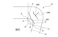
- FIG. 4A shows a cross-sectional SEM image of the tip of the cutting edge according to the third aspect of the present invention, and FIG.
- the cutting edge on the flank is A
- the cutting edge on the rake face is B.
- the perpendicular of the flank passing through A and the perpendicular of the rake face passing through B are drawn, and the intersection of both perpendiculars is set as the center O.
- the blade edge angle ⁇ is an angle formed by AOB.
- the point closest to the perpendicular of the flank passing through A is defined as C
- B Let D be the point closest to the normal of the rake face passing through.
- the occupying angle ⁇ (degrees) of continuous cracks is the angle formed by COD.
- the value calculated by the continuous crack showing the maximum value is defined as the occupation angle ⁇ of the continuous crack.
- the value of (occupation angle ⁇ of continuous crack) / (blade edge angle ⁇ ) is defined as the crack occupancy rate.
- Cutting condition A A groove cutting test of carbon steel under the conditions (referred to as cutting condition A) was performed, and the present inventions 4, 5 and comparative examples 4, 5, 9, 10 were Work material-Plane dimensions: 100mm x 250mm, thickness: 50mm JIS / S55C plate, Rotational speed: 3200 min.
- Cutting condition B Conducted a groove cutting test of carbon steel under the conditions (referred to as cutting condition B), In any groove cutting test, the flank wear width of the cutting edge was measured. The measurement results are shown in Table 4.
- WC powder, TiC powder, ZrC powder, VC powder, TaC powder, NbC powder, Cr 3 C 2 powder, TiN powder, TaN powder, and Co powder all having an average particle diameter of 1 to 3 ⁇ m are prepared as raw material powders. did. These raw material powders were blended into the blending composition shown in Table 1, wet mixed by a ball mill for 72 hours, dried, and then pressed into a green compact at a pressure of 100 MPa. The obtained green compact is sintered in a vacuum of 6 Pa at a temperature of 1400 ° C. for 1 hour. After sintering, the cutting edge portion is subjected to a honing process of R: 0.03 and further subjected to finish polishing. Thus, tool bases 6 to 10 made of WC-base cemented carbide having an ISO standard / SNGA120408 insert shape were formed.
- the surface coating insert of the present invention as the coated tool of the present invention (hereinafter referred to as the present invention 8) (hereinafter referred to as the present invention 8) by forming a hard coating layer comprising an (Al, Cr) N layer having the composition shown in Table 6 and the target average layer thickness. To 14).
- Comparative Example 2 For the purpose of comparison, the tool base (insert) 6-10 was composed of an (Al, Cr) N layer having the composition and target average layer thickness shown in Table 7 under the same conditions as in Comparative Example 1. By forming the hard coating layer, comparative surface coating inserts (hereinafter referred to as Comparative Examples 11 to 20) as comparative coating tools were manufactured.
- the crystal grain morphology of the hard coating layer in the longitudinal section was observed with a scanning electron microscope (SEM). It consisted of the following granular crystal structures.
- SEM scanning electron microscope
- the surface grain size and interface grain size of the crystal grains were determined in the same manner as in the present inventions 1 to 7 and Comparative Examples 1 to 10. Further, grains in a region up to a position 100 ⁇ m away from the cutting edge on the flank (that is, three positions, a cutting edge on the flank and a position 50 ⁇ m away from the cutting edge on the flank and a position 100 ⁇ m away from the cutting edge).
- the crystal grain length ratio occupied by crystal grains having a diameter of 0.15 ⁇ m or less was measured. Furthermore, the value of the compressive residual stress in the hard coating layer was measured. Further, the values of the blade edge angle ⁇ , the occupying angle ⁇ of the continuous crack, and the crack occupying ratio ⁇ / ⁇ were also measured and calculated. Tables 6 and 7 show the values measured and calculated above.
- the coated inserts of the present inventions 8 to 14 and Comparative Examples 11 to 20 are all screwed to the tip of the tool steel tool with a fixing jig, Work material: JIS / SCM440 round bar, Cutting speed: 150 m / min. , Incision: 1.5mm, Feed: 0.3 mm / rev. , Cutting time: 3 minutes
- a dry continuous cutting test of alloy steel (chromium molybdenum steel) under the above conditions (referred to as cutting condition C) was performed, and the flank wear width of the cutting edge was measured. The measurement results are shown in Table 8.
- the coated tool of the present invention determines the surface grain size and interface grain size of the granular crystal grains of the hard coating layer composed of the (Al, Cr) N layer within a specific numerical range, By setting the crystal grain length ratio of the crystal grains having a grain size of 0.15 ⁇ m or less in the region from the cutting edge on the flank to a position of 100 ⁇ m to 20% or less, and compressive residual stress in the hard coating layer By specifying 2.0 to 2.7 GPa, and by defining the crack occupancy rate to 0.3 to 1.0, it has excellent chipping resistance in cutting of carbon steel, alloy steel, etc. Demonstrate wearability. On the other hand, it is apparent that the comparative coated tool in which the structure of the hard coating layer is outside the range defined in the present invention reaches the service life in a relatively short time due to occurrence of chipping or a decrease in wear resistance.
- the coated tool of the present invention exhibits excellent cutting performance over a long period of time when subjected to cutting of carbon steel, alloy steel, etc. It can cope with labor saving, energy saving and cost reduction of processing sufficiently satisfactorily.
Abstract
Description
本願は、2012年3月5日に、日本に出願された特願2012-047926号、および2013年3月1日に日本に出願された特願2013-40331に基づき優先権を主張し、その内容をここに援用する。 The present invention relates to a surface-coated cutting tool (hereinafter referred to as a coated tool) that exhibits excellent chipping resistance and abrasion resistance in a cutting process such as carbon steel and alloy steel.
This application claims priority based on Japanese Patent Application No. 2012-047926 filed in Japan on March 5, 2012 and Japanese Patent Application No. 2013-40331 filed in Japan on March 1, 2013. The contents are incorporated herein.
そして、上記従来の被覆工具は、例えば、図1Aおよび図1Bに示すように、物理蒸着装置の1種であるアークイオンプレーティング装置に上記の工具基体を装入し、ヒータで工具基体を500℃の温度に加熱した状態で、アノード電極と所定組成のAl-Cr合金がセットされたカソード電極との間に、電流:90Aの条件でアーク放電を発生させ、同時に装置内に反応ガスとして窒素ガスを導入して、2Paの反応雰囲気とし、一方、上記工具基体には、-100Vのバイアス電圧を印加した条件で、上記工具基体の表面に、上記(Al,Cr)N層を蒸着形成することにより製造し得ることも知られている。 For example, as shown in Patent Document 1, as a coated tool, a composite nitride of Al and Cr is formed on the surface of a base (hereinafter referred to as a tool base) made of tungsten carbide (hereinafter referred to as WC) based cemented carbide. A coating tool formed by vapor-depositing a hard coating layer composed of a layer [hereinafter referred to as (Al, Cr) N] is known. In such a conventional coating tool, the above (Al, Since the Cr) N layer has excellent high-temperature hardness, heat resistance, high-temperature strength, high-temperature oxidation resistance, etc., it is known to exhibit excellent cutting performance.
In the conventional coated tool, for example, as shown in FIGS. 1A and 1B, the tool base is loaded into an arc ion plating apparatus which is a kind of physical vapor deposition apparatus, and the tool base is set to 500 with a heater. While being heated to a temperature of 0 ° C., an arc discharge is generated between the anode electrode and the cathode electrode on which an Al—Cr alloy having a predetermined composition is set under the condition of current: 90 A, and at the same time, nitrogen as a reaction gas in the apparatus A gas is introduced to form a reaction atmosphere of 2 Pa. On the other hand, the (Al, Cr) N layer is deposited on the surface of the tool base under the condition that a bias voltage of −100 V is applied to the tool base. It is also known that it can be manufactured.
例えば、特許文献2には、すくい面での被覆層の欠損を抑制して耐欠損性を向上させ、また、逃げ面における耐摩耗性を向上させた被覆工具として、被覆層を柱状結晶で構成し、すくい面における被覆層厚は逃げ面での被覆層厚よりも薄く、被覆層表面側の上層領域の平均結晶幅が、被覆層基体側の下層領域の平均結晶幅よりも大きい2つの層領域にて構成し、すくい面での被覆層厚に対する上層領域の厚みの比率が、逃げ面での被覆層厚に対する上層領域の厚みの比率よりも小さく、すくい面での柱状結晶の平均結晶幅が逃げ面での柱状結晶の平均結晶幅より小さい被覆工具(エンドミル)が記載されている。
また、例えば、特許文献3には、耐摩耗性と靭性とを両立させたとともに、基材との密着性にも優れた被膜を備えた被覆工具として、基材上に形成された被膜は、第1被膜層を含み、該第1被膜層は、微細組織領域と粗大組織領域とを含み、該微細組織領域は、それを構成する化合物の平均結晶粒径が10~200nmであり、かつ該第1被膜層の表面側から該第1被膜層の全体の厚みに対して50%以上の厚みとなる範囲を占めて存在し、かつ-4GPa以上-2GPa以下の範囲の応力である平均圧縮応力を有し、該第1被膜層は、その厚み方向に応力分布を有しており、その応力分布において2つ以上の極大値または極小値を持ち、それらの極大値または極小値は厚み方向表面側に位置するものほど高い圧縮応力を有する被覆工具が記載されている。 By the way, in the coated tool, various proposals have been made for the structure of the hard coating layer in order to improve its cutting performance, particularly chipping resistance, wear resistance, and the like.
For example,
Further, for example, in
上記従来の被覆工具においては、ある程度の耐チッピング性、耐欠損性、耐摩耗性の改善は図り得るものの、これを炭素鋼、合金鋼などの一段と厳しい切削加工に用いた場合には、チッピングが発生しやすく、あるいは、摩耗損耗が大きくなり、これを原因として、比較的短時間で使用寿命に至るのが現状である。 In recent years, the performance of cutting devices has been dramatically improved, while on the other hand, there has been a strong demand for labor saving, energy saving, and cost reduction for cutting, and as a result, cutting has been performed under more severe cutting conditions. It is coming.
The conventional coated tool can improve chipping resistance, chipping resistance, and wear resistance to some extent, but if it is used for more severe cutting such as carbon steel and alloy steel, chipping will not occur. It is easy to occur or wear and wear increase, and this causes the service life in a relatively short time.
(1)炭化タングステン基超硬合金で構成された工具基体の表面に、平均層厚が2~10μmの硬質被覆層を蒸着形成した表面被覆切削工具において、
(a)上記硬質被覆層は、AlとCrの複合窒化物層からなり、AlとCrの合量に占めるCrの含有割合は、0.2~0.5(但し、原子比)であり、
(b)上記表面被覆切削工具の上記工具基体の逃げ面上の刃先から、上記逃げ面上で上記逃げ面刃先から反対側に向けて100μm離れた位置までの領域上に蒸着形成された硬質被覆層は、粒状結晶組織を有し、上記領域上に形成された上記硬質被覆層表面の粒状結晶粒の平均粒径は0.2~0.5μmであり、上記領域における上記工具基体と上記硬質被覆層の界面における粒状結晶粒の平均粒径は、上記硬質被覆層表面の上記粒状結晶粒の平均粒径より0.02~0.1μm小さく、粒径が0.15μm以下の結晶粒が占める結晶粒径長割合は20%以下であることを特徴とする表面被覆切削工具。
(2)上記硬質被覆層中の圧縮残留応力は2.0~2.7GPaであることを特徴とする上記(1)に記載の被覆工具。
(3)上記被覆工具の刃先角度をα度とし、該α度の角度範囲内の切れ刃先端のコーナー部の硬質被覆層中に形成されている連続クラックの占有角度をβ度とした場合、クラック占有率β/αが0.3~1.0であることを特徴とする上記(1)または(2)に記載の被覆工具。
(4)上記粒状結晶組織に含まれる結晶粒のアスペクト比は1以上6以下であることを特徴とする上記(1)から(3)のいずれかひとつに記載の表面被覆切削工具。
(5)炭化タングステン基超硬合金で構成された工具基体の表面に、平均層厚が2~10μmの硬質被覆層を蒸着形成した表面被覆切削工具の製造方法であって、アノード電極と、Al-Cr合金からなるターゲットと、上記ターゲットの背面側に設けられた磁力発生源を備えるアークイオンプレーティング装置内に、炭化タングステン基超硬合金からなる工具基体を装入する基体装入工程と、上記工具基体上にAlとCrの複合窒化物層からなる硬質被覆層を蒸着形成する蒸着工程とを備え、上記蒸着工程は、上記アークイオンプレーティング装置内に窒素ガスを導入するガス導入工程と、上記ターゲットと上記工具基体の間に、上記磁力発生源により磁場を印加する印加工程と、上記工具基体にバイアス電圧を印加しつつ、上記ターゲットと上記アノード電極との間にアーク放電を発生させる放電工程と、上記工具基体を上記アークイオンプレーティング装置内で自転および公転させる自公転工程とを有し、上記工具基体が上記ターゲットに最接近した際には、上記工具基体の逃げ面の一部又は全部と上記ターゲットの上記工具基体側の面が水平となるように上記工具基体は支持されることを特徴とする表面被覆切削工具の製造方法。
(6)上記磁場が、積算磁力として、140~400mT×mmであることを特徴とする上記(5)記載の表面被覆切削工具の製造方法。 The present invention has been made based on the above findings and has the following aspects.
(1) In a surface-coated cutting tool in which a hard coating layer having an average layer thickness of 2 to 10 μm is vapor-deposited on the surface of a tool base composed of a tungsten carbide-based cemented carbide,
(A) The hard coating layer is composed of a composite nitride layer of Al and Cr, and the content ratio of Cr in the total amount of Al and Cr is 0.2 to 0.5 (however, the atomic ratio),
(B) Hard coating formed by vapor deposition on a region from the cutting edge on the flank of the tool base of the surface-coated cutting tool to a position 100 μm away from the flank cutting edge toward the opposite side on the flank. The layer has a granular crystal structure, and the average grain size of the granular crystal grains on the surface of the hard coating layer formed on the region is 0.2 to 0.5 μm. The average grain size of the granular crystal grains at the interface of the coating layer is 0.02 to 0.1 μm smaller than the average grain size of the granular crystal grains on the surface of the hard coating layer, and the grain size is 0.15 μm or less. A surface-coated cutting tool, wherein the crystal grain length ratio is 20% or less.
(2) The coated tool according to (1), wherein the compressive residual stress in the hard coating layer is 2.0 to 2.7 GPa.
(3) When the cutting edge angle of the coated tool is α degrees, and the occupation angle of continuous cracks formed in the hard coating layer at the corner portion of the cutting edge within the angle range of the α degrees is β degrees, The coated tool according to (1) or (2) above, wherein the crack occupation ratio β / α is 0.3 to 1.0.
(4) The surface-coated cutting tool according to any one of (1) to (3) above, wherein an aspect ratio of crystal grains contained in the granular crystal structure is 1 or more and 6 or less.
(5) A method of manufacturing a surface-coated cutting tool in which a hard coating layer having an average layer thickness of 2 to 10 μm is formed on the surface of a tool base made of a tungsten carbide-based cemented carbide, comprising an anode electrode, Al A base charging step of charging a tool base made of a tungsten carbide base cemented carbide into an arc ion plating apparatus provided with a target made of a Cr alloy and a magnetic force generation source provided on the back side of the target; A vapor deposition step of vapor-depositing and forming a hard coating layer composed of a composite nitride layer of Al and Cr on the tool base, the vapor deposition step comprising a gas introduction step of introducing nitrogen gas into the arc ion plating apparatus; An application step of applying a magnetic field by the magnetic force generation source between the target and the tool base; and applying a bias voltage to the tool base while the target is applied. A discharge process for generating an arc discharge between the electrode base and the anode electrode, and a self-revolution process for rotating and revolving the tool base in the arc ion plating apparatus, wherein the tool base is closest to the target. The tool base is supported so that a part or all of the flank of the tool base and the surface of the target on the tool base side are horizontal when the tool base is manufactured. Method.
(6) The method for producing a surface-coated cutting tool according to (5), wherein the magnetic field is 140 to 400 mT × mm as an integrated magnetic force.
図3Aは、本発明の一態様の被覆工具の縦断面概略説明図を示す。図3Aに示されるように、本願発明の被覆工具13では基体14上に硬質被覆層15が形成されている。被覆工具13の逃げ面21およびすくい面22の間に、切れ刃部が形成される。
(a)硬質被覆層の種別、平均層厚:
本願発明の被覆工具13の硬質被覆層15は、AlとCrの複合窒化物層((Al,Cr)N層)からなる。
上記(Al,Cr)N層は、Al成分が高温硬さと耐熱性を向上させ、Cr成分が高温強度を向上させ、さらにCrとAlの共存含有によって高温耐酸化性が向上することから、高温硬さ、耐熱性、高温強度及び高温耐酸化性にすぐれた硬質被覆層として既によく知られている。
Alとの合量に占めるCrの含有割合(原子比、以下同じ)が0.2未満では、切削加工時の高温強度を確保することが困難となり、一方、Alとの合量に占めるCrの含有割合(原子比)が0.5を越えると、相対的にAlの含有割合が少なくなり、高温硬さの低下、耐熱性の低下を招く。その結果、偏摩耗の発生、熱塑性変形の発生等により耐摩耗性が劣化するようになる。以上から本願発明の被覆工具における硬質被覆層15では、Alとの合量に占めるCrの含有割合(原子比)は、0.2~0.5としている。より好ましいCrの含有割合は0.22~0.45である。さらにより好ましいCrの含有割合は0.25~0.42である。
また、(Al,Cr)N層からなる硬質被覆層の平均層厚は、2μm未満では、すぐれた耐摩耗性を長期に亘って発揮することができず、工具寿命短命の原因となる。一方、その平均層厚が10μmを越えると、刃先部にチッピングが発生し易くなる。以上から、本願発明の被覆工具13における硬質被覆層15の平均層厚は2~10μmとしている。より好ましい硬質被覆層15の平均層厚は2.5~9である。さらにより好ましい平均層厚は3~8である。 Embodiments of the coated tool of the present invention will be described in detail with reference to the drawings.
FIG. 3A is a schematic explanatory view of a longitudinal section of a coated tool of one embodiment of the present invention. As shown in FIG. 3A, in the
(A) Type of hard coating layer, average layer thickness:
The
In the (Al, Cr) N layer, the Al component improves the high temperature hardness and heat resistance, the Cr component improves the high temperature strength, and the high temperature oxidation resistance is improved by the coexistence of Cr and Al. It is already well known as a hard coating layer having excellent hardness, heat resistance, high temperature strength and high temperature oxidation resistance.
If the content ratio of Cr in the total amount with Al (atomic ratio, the same applies hereinafter) is less than 0.2, it is difficult to ensure high temperature strength at the time of cutting, while Cr accounts for the total amount with Al. When the content ratio (atomic ratio) exceeds 0.5, the Al content ratio is relatively reduced, leading to a decrease in high-temperature hardness and a decrease in heat resistance. As a result, wear resistance deteriorates due to the occurrence of uneven wear, the occurrence of thermoplastic deformation, and the like. From the above, in the
Moreover, if the average thickness of the hard coating layer made of the (Al, Cr) N layer is less than 2 μm, excellent wear resistance cannot be exhibited over a long period of time, resulting in a short tool life. On the other hand, if the average layer thickness exceeds 10 μm, chipping tends to occur at the blade edge portion. From the above, the average layer thickness of the
本願発明の被覆工具13では、逃げ面21の特定領域において、さらに特殊な性質を有する硬質被覆層を形成することで、硬質被覆層中の圧縮残留応力を低減させている。
上記の逃げ面特定領域とは、逃げ面上の刃先16から、逃げ面上で、逃げ面刃先16から反対側に向けて100μm離れた位置までの領域17のことである。この領域17上に形成された硬質被覆層20は、以下に説明する特徴を有する。
上記(Al,Cr)N層からなる硬質被覆層20は粒状結晶として成膜される。さらに、この硬質被覆層20の表面19における結晶粒の平均結晶粒径(以下、単に「表面粒径」という)は0.2~0.5μmとされる。一方、工具基体14と硬質被覆層20との界面18における硬質被覆層20の結晶粒の平均結晶粒径(以下、単に「界面粒径」という)は、表面粒径より0.02~0.1μm小さい値として成膜される。すなわち、この領域17上では、表面粒径と界面粒径とがそれぞれ異なる平均結晶粒径範囲となるように、硬質被覆層20の結晶組織構造が形成されている。これにより、硬質被覆層中に形成される圧縮残留応力が所定数値範囲内となるように成膜される。
ここで、「工具基体と硬質被覆層の界面における硬質被覆層の結晶粒」とは、硬質被覆層内における工具基体14と硬質被覆層20の界面から厚さ0.5μmの硬質被覆層内部の領域に形成されている結晶粒を意味する。また、「硬質被覆層表面における結晶粒」とは、硬質被覆層20の表面から深さ0.5μmの領域に形成されている結晶粒を意味する。
また、ここで「粒状結晶」とは、「柱状結晶」と区別するために使用している用語であり、具体的には、その結晶粒のアスペクト比が1以上6以下であることを意味する。アスペクト比は、結晶粒断面で最も長い直径(長辺)とそれに垂直な直径(短辺)の長さの比を、長辺を分子、短辺を分母として算出する。 (B) Layer structure of hard coating layer composed of (Al, Cr) N layer:
In the
The above flank specific area is a
The
Here, “the crystal grains of the hard coating layer at the interface between the tool base and the hard coating layer” means the inside of the hard coating layer having a thickness of 0.5 μm from the interface between the
The term “granular crystal” used herein is a term used to distinguish from “columnar crystal”, and specifically means that the aspect ratio of the crystal grain is 1 or more and 6 or less. . The aspect ratio is calculated as the ratio of the longest diameter (long side) to the diameter (short side) perpendicular to the crystal grain cross section, with the long side as the numerator and the short side as the denominator.
硬質被覆層表面19における結晶粒の平均結晶粒径(表面粒径)が0.2μm未満であると、硬質被覆層中の圧縮残留応力が大きくなるため、切削加工時にチッピングを発生しやすくなる。一方、表面粒径が0.5μmを超えると、圧縮残留応力が小さくなるため、切削加工時の摩耗量が増大し、長期の使用にわたって十分な耐摩耗性を発揮することができなくなる。以上から、本願発明の被覆工具13における硬質被覆層20では、表面粒径は0.2~0.5μmと定めた。
工具基体14と硬質被覆層20の界面18における硬質被覆層20の結晶粒の平均結晶粒径(界面粒径)については、表面粒径よりも0.02~0.1μmだけ小さい値とすることが必要である。その技術的な理由は、表面粒径より0.1μmを超えて界面粒径が小さい場合には、表面粒径と界面粒径の差が大きくなる事により、それぞれの部分での圧縮残留応力の差が大きくなり、膜全体で脆化してしまう。そのため、切削時に摩耗やチッピングがしやすくなり、切削性能が悪化する問題が生じる。
一方、界面粒径と表面粒径との差が0.02μm以内である場合には、表面と界面で圧縮残留応力の差が同等となり、切削を行った際に、耐摩耗性の向上の作用を付与できない、ということによる。
なお、本発明では、表面粒径よりも界面粒径を0.02~0.1μm小さい値にする事で、膜全体が脆化しない程度に界面側での圧縮残留応力を大きくし、長時間切削を行った際に、膜表面が摩耗した後も界面側の摩耗を抑制させる作用を付与する。
粒径の測定方法を以下に図3Bを参照して記述する。工具基体刃先から逃げ面側の断面を切り出し、その断面をSEMにて観察する。硬質被覆層表面19から深さ0.5μmの領域に形成されている各結晶粒を用い、工具基体表面と平行に直線を引き、結晶粒界間の距離を粒径と定義する。なお、工具基体表面と平行に直線を引く位置は、各結晶粒において最長の結晶粒径となる位置とする。逃げ面上の刃先16から100μm離れた位置までの領域17において結晶粒径を測定し、その平均結晶粒径の平均値を表面粒径とする。より具体的にいえば、逃げ面上の刃先16及び逃げ面上において刃先から50μm離れた位置、及び刃先から100μm離れた位置の3箇所で、幅10μmの範囲内(図3Bにおいて、硬質被覆層20中に点線で示されている領域)に存在する結晶の平均結晶粒径を測定し、さらに、その3箇所での平均結晶粒径の平均値を表面粒径とする。また、硬質被覆層内における工具基体14と硬質被覆層20の界面18から厚さ0.5μmの領域に形成されている各結晶粒においても同様の方法にて界面粒径を算出する。 The average crystal grain size will be specifically described as follows.
When the average crystal grain size (surface grain size) of the crystal grains on the hard
The average crystal grain size (interface grain size) of the crystal grains of the
On the other hand, when the difference between the interface particle size and the surface particle size is within 0.02 μm, the difference in compressive residual stress between the surface and the interface becomes the same, and the effect of improving the wear resistance when cutting is performed. Because it cannot be granted.
In the present invention, by setting the interface particle size to a value smaller by 0.02 to 0.1 μm than the surface particle size, the compressive residual stress on the interface side is increased to such an extent that the entire film does not become brittle. When cutting is performed, an action of suppressing wear on the interface side is imparted even after the film surface is worn.
The particle size measurement method is described below with reference to FIG. 3B. A section on the flank side is cut out from the tool base blade edge, and the section is observed with an SEM. Using each crystal grain formed in a region having a depth of 0.5 μm from the hard
ここで「粒径が0.15μm以下の結晶粒が占める結晶粒径長割合」とは、複数の結晶粒の粒径を測定し、その全測定結晶粒径長の和に対する粒径0.15μm以下の結晶粒径長の和の割合を示す。
また、「刃先」とは、図3Aから図3Cに示すように、「切れ刃先端のコーナー部の円錐形状となっている部分を除いた、直線状切れ刃の最も先端に近い部分」であると、本発明では定義する。
図3Cは、本発明の一態様の被覆工具の縦断面概略説明図を示し、基体逃げ面及び基体すくい面の仮想延長線の交点と、逃げ面上の刃先との位置関係を示す図である。図3Cでは、基体のみが示され、硬質被覆層は示されていない。
図3Cに示すように、基体逃げ面21および基体すくい面22の仮想延長線の交点23と、逃げ面上の刃先16との距離L(μm)には以下の関係がある。
距離L、コーナー部の円弧の半径r(μm)、および基体逃げ面21と基体すくい面22の仮想延長線がなす角度θ(度)には、「L=r/tan(0.5×θ)」の関係が成立する。 Further, a
Here, “the ratio of the crystal grain length occupied by crystal grains having a grain size of 0.15 μm or less” means that the grain diameter of a plurality of crystal grains is measured, and the grain diameter is 0.15 μm relative to the sum of all the measured crystal grain lengths. The ratio of the sum of the following crystal grain lengths is shown.
In addition, as shown in FIGS. 3A to 3C, the “blade tip” is “the portion closest to the tip of the linear cutting blade excluding the conical portion of the corner portion at the tip of the cutting blade”. This is defined in the present invention.
FIG. 3C is a longitudinal cross-sectional schematic explanatory diagram of the coated tool of one embodiment of the present invention, and is a diagram illustrating the positional relationship between the intersection of the virtual extension line of the base flank and the base rake face and the cutting edge on the flank. . In FIG. 3C, only the substrate is shown and the hard coating layer is not shown.
As shown in FIG. 3C, the distance L (μm) between the
The distance L, the radius r (μm) of the arc of the corner portion, and the angle θ (degree) formed by the virtual extension line of the base flank 21 and the base rake face 22 are expressed as “L = r / tan (0.5 × θ ) ”Is established.
その理由は、次のとおりである。
工具基体表面に、アークイオンプレーティング装置(AIP装置)を用いて硬質被覆層を形成する場合、層中には圧縮残留応力が蓄積され、特に、結晶粒径の大きな層にあっては、結晶粒界に圧縮残留応力が集中し、亀裂の起点となりやすい。
しかし、本願発明の被覆工具13によれば、切れ刃先端のコーナー部の硬質被覆層中に予めクラックCが形成されていることから、残留応力の集中が低減されるため、特に、切削開始初期のチッピング発生等による切削性能の低下を抑制することができる。
ただし、β/αが0.3未満である場合には、圧縮残留応力の集中抑制効果を期待することはできないので、β/αは0.3以上と定めた。
圧縮残留応力の集中抑制効果の観点からは、β/αの値に上限を設ける必要はない(即ち、β/αは、0.3~1.0)が、β/αの値が1.0に近づくほど、硬質被覆層と工具基体界面での界面剥離が発生しやすくなるので、β/αの値は、0.3~0.9であることが好ましい。さらに好ましいβ/αの範囲は、0.4~0.85である。 In the
The reason is as follows.
When a hard coating layer is formed on the surface of a tool base using an arc ion plating apparatus (AIP apparatus), compressive residual stress is accumulated in the layer, and particularly in a layer having a large crystal grain size, Compressive residual stress concentrates on the grain boundary and tends to be the origin of cracks.
However, according to the
However, when β / α is less than 0.3, the effect of suppressing the concentration of compressive residual stress cannot be expected, so β / α is set to 0.3 or more.
From the viewpoint of the effect of suppressing the concentration of compressive residual stress, there is no need to set an upper limit for the value of β / α (that is, β / α is 0.3 to 1.0), but the value of β / α is 1. The closer to 0, the easier the interface peeling at the hard coating layer / tool base interface occurs, so the value of β / α is preferably 0.3 to 0.9. A more preferable range of β / α is 0.4 to 0.85.
本願発明におけるクラックとは、切れ刃先端のコーナー部を含む硬質被覆層中に形成された亀裂を意味する。このクラックは例えば被覆工具の断面SEM写真を例えば10000倍の倍率で観察することで確認することができる。本願発明におけるクラックは、幅が30nm以上の亀裂を意味している。クラックの幅が端部で先細りしてゆき、クラックの幅が30nm未満となった点をクラックの端部と規定する。
ここで、クラック占有率とは、本発明で、以下のように定義する。
図4Aおよび図4Bに示すように、逃げ面上の刃先Aを通る逃げ面の垂線と、すくい面上の刃先Bを通るすくい面の垂線との交点を中心Oとした時、A-O-Bのなす角度を刃先角度α(度)という。
また、切れ刃先端のコーナー部の硬質被覆層中に形成されている連続クラックについては、上記中心Oから、連続する一つのクラックの端部C,Dに接する線を引いた時、C-O-Dのなす角度を連続クラックの占有角度β(度)とする。切れ刃先端のコーナー部の硬質被覆層中に複数のクラックが存在する場合、最大の占有角度を示す連続クラックを用いるものとする。
そして、(連続クラックの占有角度β)/(刃先角度α)の値を、クラック占有率であると定義する。
なお、本発明被覆工具は、(Al,Cr)N層からなる硬質被覆層の平均層厚を2~10μm、AlとCrの合量に占めるCrの含有割合は0.2~0.5(但し、原子比)、粒状結晶粒の表面粒径、界面粒径を特定の数値範囲に定め、また、逃げ面上の刃先16から100μm離れた位置までの領域17における粒径が0.15μm以下の結晶粒が占める結晶粒径長割合を20%以下と定めることにより、硬質被覆層中の圧縮残留応力の値が2.0~2.7GPaであり、さらに刃先のクラック占有率β/αが0.3~1である被覆切削工具を効率良く製造することができる。 Here, the definition of the crack in this invention is demonstrated first.
The crack in this invention means the crack formed in the hard coating layer containing the corner part of a cutting-blade front-end | tip. This crack can be confirmed by, for example, observing a cross-sectional SEM photograph of the coated tool at a magnification of 10,000 times, for example. The crack in the present invention means a crack having a width of 30 nm or more. The point where the width of the crack tapers at the end and the width of the crack is less than 30 nm is defined as the end of the crack.
Here, the crack occupation ratio is defined as follows in the present invention.
As shown in FIGS. 4A and 4B, when the intersection point of the perpendicular of the flank passing through the cutting edge A on the flank and the perpendicular of the rake face passing through the cutting edge B on the rake face is defined as AO- The angle formed by B is called the blade edge angle α (degrees).
For continuous cracks formed in the hard coating layer at the corner at the tip of the cutting edge, when a line in contact with the ends C and D of one continuous crack is drawn from the center O, C—O The angle formed by −D is defined as the occupation angle β (degrees) of the continuous crack. When there are a plurality of cracks in the hard coating layer at the corner portion at the tip of the cutting edge, a continuous crack showing the maximum occupation angle is used.
The value of (occupation angle β of continuous crack) / (blade edge angle α) is defined as the crack occupancy rate.
In the coated tool of the present invention, the average layer thickness of the hard coating layer composed of the (Al, Cr) N layer is 2 to 10 μm, and the content ratio of Cr in the total amount of Al and Cr is 0.2 to 0.5 ( However, the atomic ratio), the surface grain size of the granular crystal grains, and the interface grain size are set in specific numerical ranges, and the grain size in the
この発明の硬質被覆層は、図2Aおよび図2Bに示すようなアークイオンプレーティング装置(AIP装置)を用い、工具基体の温度を370~450℃に維持しつつ、工具基体をAIP装置内で自転および公転させ、ターゲット表面中心とターゲットに最近接した工具基体間に所定の磁場(積算磁力が140~400mT×mm)を印加しながら蒸着することによって、形成することができる。
例えば、AIP装置の一方には基体洗浄用のTi電極からなるカソード電極、他方にはAl-Cr合金からなるターゲット(カソード電極)を設ける。このAl-Cr合金中のAl含量は55at%Al~78at%Alが好ましい。Cr含量は、上記Al含量に対応して、22at%Cr~45at%Crが好ましい。例えば、70at%Al-30at%Cr合金からなるターゲット(カソード電極)を設ける。
まず、炭化タングステン(WC)基超硬合金からなる工具基体を洗浄・乾燥し、AIP装置内の回転テーブル上に装着し、真空中で基体洗浄用のTi電極とアノード電極との間に100Aのアーク放電を発生させて、工具基体に-1000Vのバイアス電圧を印加しつつ工具基体表面をボンバード洗浄する。
ついで、Al-Cr合金ターゲットの表面中心からターゲットに最近接した工具基体までの積算磁力が140~400mT×mmなる磁場を印加する。
ついで、装置内に反応ガスとして窒素ガスを導入する。これにより装置内の雰囲気圧力は、9.0Pa~9.6Paの範囲内に保たれる。例えば、9.3Paの雰囲気圧力とされる。さらに、工具基体の温度を370~450℃に維持し、工具基体に-50Vのバイアス電圧を印加しつつ、Al-Cr合金ターゲット(カソード電極)とアノード電極との間に100Aのアーク放電を発生させる。工具基体がターゲットに最接近した際には、逃げ面の一部又は全部とターゲット面が水平となるように工具基体を支持して自公転させつつ蒸着することによって、本願発明の被覆工具13の有する硬質被覆層を蒸着形成することができる。
なお、上記のAl-Cr合金ターゲットと工具基体間での磁場の印加は、例えば、カソード周辺に磁場発生源である電磁コイル又は永久磁石を設置する、あるいは、AIP装置の内部、中心部に永久磁石を配置する等、任意の手段で磁場を形成することができる。 (C) Vapor deposition of hard coating layer The hard coating layer of the present invention uses an arc ion plating apparatus (AIP apparatus) as shown in FIGS. 2A and 2B, and maintains the temperature of the tool base at 370 to 450 ° C. On the other hand, the tool base is rotated and revolved in the AIP apparatus, and is deposited by applying a predetermined magnetic field (integrated magnetic force 140 to 400 mT × mm) between the center of the target surface and the tool base closest to the target. can do.
For example, a cathode electrode made of a Ti electrode for substrate cleaning is provided on one side of the AIP apparatus, and a target (cathode electrode) made of an Al—Cr alloy is provided on the other side. The Al content in this Al—Cr alloy is preferably 55 at% Al to 78 at% Al. The Cr content is preferably 22 at% Cr to 45 at% Cr corresponding to the Al content. For example, a target (cathode electrode) made of a 70 at% Al-30 at% Cr alloy is provided.
First, a tool substrate made of tungsten carbide (WC) -based cemented carbide is cleaned and dried, mounted on a rotary table in an AIP apparatus, and 100 A between the Ti electrode and the anode electrode for cleaning the substrate in vacuum. An arc discharge is generated to bombard the surface of the tool base while applying a bias voltage of −1000 V to the tool base.
Next, a magnetic field having an integrated magnetic force of 140 to 400 mT × mm from the center of the surface of the Al—Cr alloy target to the tool base closest to the target is applied.
Subsequently, nitrogen gas is introduced into the apparatus as a reaction gas. As a result, the atmospheric pressure in the apparatus is maintained in the range of 9.0 Pa to 9.6 Pa. For example, the atmospheric pressure is set to 9.3 Pa. Furthermore, while maintaining the temperature of the tool base at 370 to 450 ° C. and applying a bias voltage of −50 V to the tool base, a 100 A arc discharge is generated between the Al—Cr alloy target (cathode electrode) and the anode electrode. Let When the tool base is closest to the target, vapor deposition is performed while supporting and revolving the tool base so that part or all of the flank and the target surface are horizontal. The hard coating layer can be formed by vapor deposition.
The application of the magnetic field between the Al—Cr alloy target and the tool base is performed by, for example, installing an electromagnetic coil or permanent magnet as a magnetic field generation source around the cathode, or by permanent attachment in the center of the AIP device. The magnetic field can be formed by any means such as disposing a magnet.
(b)次に、装置内を排気して真空に保持しながら、ヒータで工具基体を400℃に加熱した後、上記回転テーブル上で自転しながら回転する工具基体に-1000Vの直流バイアス電圧を印加し、かつ、Tiカソード電極とアノード電極との間に100Aの電流を流してアーク放電を発生させた。上記の手順により、工具基体表面はボンバード洗浄される。
(c)ついで、上記Al-Cr合金ターゲットの表面中心から工具基体までの積算磁力が140~400mT×mmの範囲内となるように種々の磁場を印加し。
(d)ついで、装置内に反応ガスとして窒素ガスを導入して9.3Paの反応雰囲気とした。上記手順と同時に、上記回転テーブル上で自転しながら回転する工具基体の温度を370~450℃の範囲内に維持するとともに-50Vの直流バイアス電圧を印加し、かつ上記Al-Cr合金ターゲットとアノード電極との間に100Aの電流を流してアーク放電を発生させた。上記の手順により、上記工具基体の表面に、表2に示される組成および目標平均層厚の(Al,Cr)N層からなる硬質被覆層を蒸着形成した。
上記の工程(a)から(d)を経て、本発明の被覆工具としての表面被覆エンドミル1~7(以下、本発明1~7という)をそれぞれ製造した。
なお、図2Aおよび図2Bに示すAIP装置では、工具基体がAl-Cr合金ターゲットに最接近する際に、逃げ面の一部又は全部とAl-Cr合金ターゲット面が水平となるように装着支持した。 (A) Each of the tool bases 1 to 5 is ultrasonically cleaned in acetone and dried, and is separated from the central axis on the rotary table of the AIP apparatus shown in FIGS. 2A and 2B by a predetermined distance in the radial direction. Attached along the outer periphery at the position. A Ti cathode electrode for bombard cleaning was placed on one side of the AIP apparatus, and a target (cathode electrode) made of a 70 at% Al-30 at% Cr alloy was placed on the other side.
(B) Next, the tool base is heated to 400 ° C. with a heater while the apparatus is evacuated and kept in vacuum, and then a DC bias voltage of −1000 V is applied to the tool base that rotates while rotating on the rotary table. And an arc discharge was generated by applying a current of 100 A between the Ti cathode electrode and the anode electrode. The surface of the tool base is bombarded by the above procedure.
(C) Next, various magnetic fields are applied so that the integrated magnetic force from the center of the surface of the Al—Cr alloy target to the tool base is in the range of 140 to 400 mT × mm.
(D) Next, nitrogen gas was introduced as a reaction gas into the apparatus to form a reaction atmosphere of 9.3 Pa. Simultaneously with the above procedure, the temperature of the tool base rotating while rotating on the rotary table is maintained within a range of 370 to 450 ° C., a DC bias voltage of −50 V is applied, and the Al—Cr alloy target and anode An arc discharge was generated by flowing a current of 100 A between the electrodes. By the above procedure, a hard coating layer composed of an (Al, Cr) N layer having the composition and target average layer thickness shown in Table 2 was formed by vapor deposition on the surface of the tool base.
Through the above steps (a) to (d), surface-coated end mills 1 to 7 (hereinafter referred to as the present invention 1 to 7) as the coated tools of the present invention were produced.
In the AIP apparatus shown in FIGS. 2A and 2B, when the tool base is closest to the Al—Cr alloy target, it is mounted and supported so that part or all of the flank and the Al—Cr alloy target surface are horizontal. did.
比較の目的で、上記実施例1における(c)の条件を変更し(即ち、Al-Cr合金ターゲットの表面中心から工具基体までの積算磁力を140mT×mm未満、あるいは400mT×mmを超える)、また、(d)の条件を変更し(即ち、工具基体が370℃未満、あるいは450℃を超える温度に維持し)て、その他は実施例1と同一の条件で、比較例被覆工具としての表面被覆エンドミル1~5(以下、比較例1~5という)をそれぞれ製造した。さらに、実施例1から被覆層中のAlとCrの合量に占めるCrの含有割合が0.2~0.5の範囲外、被覆層の平均層厚が2~10μmの範囲外の表面被覆エンドミル6~10をそれぞれ製造した。 Comparative Example 1:
For the purpose of comparison, the condition of (c) in Example 1 was changed (that is, the integrated magnetic force from the center of the surface of the Al—Cr alloy target to the tool substrate was less than 140 mT × mm, or more than 400 mT × mm). Further, the surface of the comparative coated tool was changed under the same conditions as in Example 1 except that the condition of (d) was changed (that is, the tool base was maintained at a temperature lower than 370 ° C. or higher than 450 ° C.). Coated end mills 1 to 5 (hereinafter referred to as Comparative Examples 1 to 5) were produced. Further, the surface coating in which the content ratio of Cr in the total amount of Al and Cr in the coating layer is outside the range of 0.2 to 0.5 and the average thickness of the coating layer is outside the range of 2 to 10 μm from Example 1.
さらに、該粒状結晶の結晶粒径を走査型電子顕微鏡(SEM)で測定し、逃げ面上の刃先から100μm離れた位置までの領域における表面粒径、界面粒径を求めた。具体的には、逃げ面上の刃先、及び逃げ面上において刃先から50μm離れた位置、及び刃先から100μm離れた位置の3箇所にて、幅10μmの範囲内に存在する結晶の平均粒径を算出し、3箇所の位置での平均値を算出することから求めた。
また、同様にして、逃げ面上の刃先から100μm離れた位置までの領域において、粒径が0.15μm以下の結晶粒が占める結晶粒径長割合を、逃げ面上の刃先、及び逃げ面上において刃先から50μm離れた位置、及び刃先から100μm離れた位置での界面及び表面の計6箇所にて測定することにより求めた。
表2、表3に、上記で測定・算出したそれぞれの値を示す。 With respect to the present inventions 1 to 7 and Comparative Examples 1 to 10 produced above, the crystal grain morphology of the hard coating layer in the longitudinal section was observed, and both were composed of a granular crystal structure having an aspect ratio of 1 or more and 6 or less. It was. The aspect ratio is calculated as the ratio of the length of the longest diameter (long side) to the diameter (short side) perpendicular to the crystal grain cross section, with the long side as the numerator and the short side as the denominator.
Furthermore, the crystal grain size of the granular crystal was measured with a scanning electron microscope (SEM), and the surface grain size and the interface grain size in the region up to a position 100 μm away from the cutting edge on the flank were obtained. Specifically, the average grain size of crystals existing within a range of 10 μm in width at the three positions of the cutting edge on the flank, the position 50 μm away from the cutting edge, and the position 100 μm away from the cutting edge on the flank. It calculated and calculated | required from calculating the average value in three positions.
Similarly, in the region from the cutting edge on the flank to a position 100 μm away, the crystal grain size ratio occupied by the crystal grains having a grain size of 0.15 μm or less is set to the cutting edge on the flank and the flank. Was measured at a total of 6 locations on the interface and surface at a position 50 μm away from the blade edge and at a position 100 μm away from the blade edge.
Tables 2 and 3 show the values measured and calculated above.
被覆工具の切れ刃先端のコーナー部を含み、逃げ面の断面を研磨加工した後、その断面をSEM像にて、観察する。測定条件として、観察倍率:10000倍、加速電圧:3kVの条件を使用した。硬質被覆層表面から深さ0.5μmの領域に形成されている各結晶粒を用い、工具基体表面と平行に直線を引き、結晶粒界間の距離を粒径と定義する。なお、工具基体表面と平行に直線を引く位置は、各結晶粒において最長の結晶粒径となる位置とする。逃げ面上の刃先から100μm離れた位置までの領域、具体的な測定点としては、逃げ面上の刃先、及び逃げ面上において刃先から50μm離れた位置、及び刃先から100μm離れた位置の3箇所で、幅10μmの範囲内に存在する結晶の結晶粒径を測定し、さらに、その3箇所での平均結晶粒径の平均値を表面粒径とした。幅10μmの粒径を測定するにあたり、各測定箇所を中心に刃先側5μm、刃先と逆側5μmの測定データを用いた。ただし、逃げ面上の刃先の箇所においては、刃先から5μm離れた位置を中心として、刃先側5μm、刃先と逆側5μmの幅10μmの範囲内で測定した。また、硬質被覆層内における工具基体と硬質被覆層の界面から厚さ0.5μmの領域に形成されている各結晶粒においても同様の方法にて界面粒径を算出した。
また、粒径が0.15μm以下の結晶粒が占める結晶粒径長割合の測定方法は、上記粒径を測定した界面3箇所、及び表面3箇所にて測定した結晶粒径の全測定データを用いる。測定した全結晶粒径の和に対する、粒径が0.15μm以下の結晶粒径の和を粒径が0.15μm以下の結晶粒が占める結晶粒径長割合とした。 More specifically, the measurement method of the crystal grain size and the measurement method of the crystal grain size length ratio occupied by crystal grains having a grain size of 0.15 μm or less are as follows.
After polishing the cross section of the flank, including the corner at the tip of the coated tool, the cross section is observed with an SEM image. As measurement conditions, an observation magnification of 10000 times and an acceleration voltage of 3 kV were used. Each crystal grain formed in a region having a depth of 0.5 μm from the surface of the hard coating layer is used, a straight line is drawn parallel to the tool base surface, and the distance between crystal grain boundaries is defined as the grain size. The position where a straight line is drawn parallel to the surface of the tool base is the position where the longest crystal grain size is obtained in each crystal grain. The area from the cutting edge on the flank to the position 100 μm away, and specific measurement points include the cutting edge on the flank, the position on the flank 50 μm away from the cutting edge, and the position 100 μm away from the cutting edge. Then, the crystal grain size of the crystals existing within the range of 10 μm in width was measured, and the average value of the average crystal grain sizes at the three locations was defined as the surface grain size. In measuring a particle diameter of 10 μm in width, measurement data of 5 μm on the blade edge side and 5 μm on the opposite side to the blade edge were used centering on each measurement point. However, at the position of the cutting edge on the flank, the measurement was performed within a range of 10 μm in width of 5 μm on the side of the cutting edge and 5 μm on the opposite side to the cutting edge, with a
Moreover, the measuring method of the crystal grain size length ratio occupied by crystal grains having a grain size of 0.15 μm or less is obtained by measuring all the measurement data of the crystal grain sizes measured at the three interfaces and the three surfaces where the above-mentioned particle size was measured. Use. The sum of the crystal grain sizes with a grain size of 0.15 μm or less relative to the sum of the total crystal grain sizes measured was defined as the ratio of the crystal grain length occupied by the crystal grains with a grain size of 0.15 μm or less.
表2、表3に、上記で測定した圧縮残留応力値を示す。 Furthermore, the value of the compressive residual stress in the hard coating layer was calculated by using the peak of the AlCrN (420) plane by the 2θ-sin 2 φ method using X-ray diffraction.
Tables 2 and 3 show the compressive residual stress values measured above.
表2、表3に、これらの値を示す。
なお、上記刃先角度α、連続クラックの占有角度βの測定法をより具体的にいえば、以下のとおりである。
結晶粒径を測定するために観察したSEM像のうち、切れ刃先端部の断面SEM像を用いる。測定条件は、観察倍率:10000倍、加速電圧:3kVの条件を使用した。本発明3の切れ刃先端部の断面SEM像を図4Aに、模式図を図4Bに示す。以下、図4Bを用いて説明する。ここでは、逃げ面上の刃先をA、すくい面上の刃先をBとする。Aを通る逃げ面の垂線、Bを通るすくい面の垂線を引き、双方の垂線の交点を中心Oとする。刃先角度α(度)はA-O-Bのなす角度とする。
また、切れ刃先端のコーナー部の硬質被覆層中に形成されている連続クラックについて、上記中心Oから該クラックを投影させた場合、Aを通る逃げ面の垂線に最も近い箇所をCとし、Bを通るすくい面の垂線に最も近い箇所をDとする。連続クラックの占有角度β(度)はC-O-Dのなす角度とする。なお、切れ刃先端のコーナー部の硬質被覆層中に複数のクラックが存在する場合、最大値を示す連続クラックにて算出した値を連続クラックの占有角度βと定義する。
そして、(連続クラックの占有角度β)/(刃先角度α)の値を、クラック占有率であると定義する。 Further, the cutting edge angle α of the present inventions 1 to 7 and Comparative Examples 1 to 10 was measured, and the occupying angle β of the continuous crack in the hard coating layer at the corner portion at the tip of the cutting edge was measured. The value of α was calculated.
Tables 2 and 3 show these values.
More specifically, the measurement method of the cutting edge angle α and the occupying angle β of the continuous crack is as follows.
Of the SEM images observed for measuring the crystal grain size, a cross-sectional SEM image of the tip of the cutting edge is used. The measurement conditions used were an observation magnification of 10,000 times and an acceleration voltage of 3 kV. FIG. 4A shows a cross-sectional SEM image of the tip of the cutting edge according to the third aspect of the present invention, and FIG. Hereinafter, a description will be given with reference to FIG. 4B. Here, the cutting edge on the flank is A, and the cutting edge on the rake face is B. The perpendicular of the flank passing through A and the perpendicular of the rake face passing through B are drawn, and the intersection of both perpendiculars is set as the center O. The blade edge angle α (degrees) is an angle formed by AOB.
Further, regarding the continuous crack formed in the hard coating layer at the corner portion at the tip of the cutting edge, when the crack is projected from the center O, the point closest to the perpendicular of the flank passing through A is defined as C, and B Let D be the point closest to the normal of the rake face passing through. The occupying angle β (degrees) of continuous cracks is the angle formed by COD. When there are a plurality of cracks in the hard coating layer at the corner portion at the tip of the cutting edge, the value calculated by the continuous crack showing the maximum value is defined as the occupation angle β of the continuous crack.
The value of (occupation angle β of continuous crack) / (blade edge angle α) is defined as the crack occupancy rate.


本発明1~3、6、7および比較例1~3、6~8については、
被削材-平面寸法:100mm×250mm、厚さ:50mmのJIS・S55Cの板材、
回転速度: 16000 min.-1、
縦方向切り込み: 2.0 mm、
横方向切り込み: 0.3 mm
送り速度(1刃当り): 0.06 mm/tooth、
切削長:340m、
の条件(切削条件Aという)での炭素鋼の溝切削加工試験を実施し、また、本発明4、5および比較例4、5、9、10については、
被削材-平面寸法:100mm×250mm、厚さ:50mmの
JIS・S55Cの板材、
回転速度: 3200 min.-1、
縦方向切り込み: 10mm、
横方向切り込み: 1mm
送り速度(1刃当り): 0.07 mm/tooth、
切削長:90m、
の条件(切削条件Bという)での炭素鋼の溝切削加工試験を実施し、
いずれの溝切削加工試験でも切刃の逃げ面摩耗幅を測定した。
この測定結果を表4に示した。 Next, among the end mills of the present inventions 1 to 7 and Comparative Examples 1 to 10,
For Inventions 1-3, 6, 7 and Comparative Examples 1-3, 6-8,
Work material-Plane dimensions: 100mm x 250mm, thickness: 50mm JIS / S55C plate,
Rotational speed: 16000 min. -1 ,
Longitudinal cut: 2.0 mm,
Horizontal infeed: 0.3 mm
Feed rate (per blade): 0.06 mm / tooth,
Cutting length: 340m,
A groove cutting test of carbon steel under the conditions (referred to as cutting condition A) was performed, and the
Work material-Plane dimensions: 100mm x 250mm, thickness: 50mm JIS / S55C plate,
Rotational speed: 3200 min. -1 ,
Longitudinal cut: 10mm,
Horizontal cut: 1mm
Feed rate (per tooth): 0.07 mm / tooth,
Cutting length: 90m,
Conducted a groove cutting test of carbon steel under the conditions (referred to as cutting condition B),
In any groove cutting test, the flank wear width of the cutting edge was measured.
The measurement results are shown in Table 4.

比較の目的で、上記の工具基体(インサート)6-10に対して、上記比較例1と同一の条件で、表7に示される組成および目標平均層厚の(Al,Cr)N層からなる硬質被覆層を形成することにより、比較例被覆工具としての比較例表面被覆インサート(以下、比較例11~20という)をそれぞれ製造した。 Comparative Example 2:
For the purpose of comparison, the tool base (insert) 6-10 was composed of an (Al, Cr) N layer having the composition and target average layer thickness shown in Table 7 under the same conditions as in Comparative Example 1. By forming the hard coating layer, comparative surface coating inserts (hereinafter referred to as Comparative Examples 11 to 20) as comparative coating tools were manufactured.
また、上記で作製した本発明8~14および比較例11~20について、本発明1~7、比較例1~10の場合と同様に結晶粒の表面粒径、界面粒径を求めた。
また、逃げ面上の刃先から100μm離れた位置までの領域(即ち、逃げ面上の刃先、及び逃げ面上において刃先から50μm離れた位置、及び刃先から100μm離れた位置の3箇所)における、粒径が0.15μm以下の結晶粒が占める結晶粒径長割合を測定した。
さらに、硬質被覆層中の圧縮残留応力の値を測定した。
また、刃先角度α、連続クラックの占有角度β、クラック占有率β/αの値についても測定・算出した。
表6、表7に、上記で測定・算出したそれぞれの値を示す。 Regarding the
For the
Further, grains in a region up to a position 100 μm away from the cutting edge on the flank (that is, three positions, a cutting edge on the flank and a position 50 μm away from the cutting edge on the flank and a position 100 μm away from the cutting edge). The crystal grain length ratio occupied by crystal grains having a diameter of 0.15 μm or less was measured.
Furthermore, the value of the compressive residual stress in the hard coating layer was measured.
Further, the values of the blade edge angle α, the occupying angle β of the continuous crack, and the crack occupying ratio β / α were also measured and calculated.
Tables 6 and 7 show the values measured and calculated above.


被削材:JIS・SCM440の丸棒、
切削速度:150m/min.、
切り込み:1.5mm、
送り:0.3mm/rev.、
切削時間:3分、
の条件(切削条件Cという)での合金鋼(クロムモリブデン鋼)の乾式連続切削加工試験を実施し、切刃の逃げ面摩耗幅を測定した。
この測定結果を表8に示した。 Next, the coated inserts of the
Work material: JIS / SCM440 round bar,
Cutting speed: 150 m / min. ,
Incision: 1.5mm,
Feed: 0.3 mm / rev. ,
Cutting time: 3 minutes
A dry continuous cutting test of alloy steel (chromium molybdenum steel) under the above conditions (referred to as cutting condition C) was performed, and the flank wear width of the cutting edge was measured.
The measurement results are shown in Table 8.

これに対して、硬質被覆層の構造が本発明で規定する範囲を外れる比較例被覆工具では、チッピング発生あるいは耐摩耗性の低下によって、比較的短時間で使用寿命に至ることが明らかである。 From the results shown in Tables 4 and 8, the coated tool of the present invention determines the surface grain size and interface grain size of the granular crystal grains of the hard coating layer composed of the (Al, Cr) N layer within a specific numerical range, By setting the crystal grain length ratio of the crystal grains having a grain size of 0.15 μm or less in the region from the cutting edge on the flank to a position of 100 μm to 20% or less, and compressive residual stress in the hard coating layer By specifying 2.0 to 2.7 GPa, and by defining the crack occupancy rate to 0.3 to 1.0, it has excellent chipping resistance in cutting of carbon steel, alloy steel, etc. Demonstrate wearability.
On the other hand, it is apparent that the comparative coated tool in which the structure of the hard coating layer is outside the range defined in the present invention reaches the service life in a relatively short time due to occurrence of chipping or a decrease in wear resistance.
2 チャンバー
3 回転テーブル
4 超硬基体
5 ヒーター
6 アノード電極
7 カソード電極
8 磁力発生源
9 反応ガス導入口
10 排ガス口
11 バイアス電源
12 アーク電源
13 被覆切削工具
14 工具基体
15 硬質被覆層
16、A 逃げ面刃先
B すくい面刃先
17 逃げ面刃先15から100μm離れた位置までの領域
18 領域16における工具基体と硬質被覆層との界面
19 領域16上に形成された硬質被覆層表面
20 領域16上に形成された硬質被覆層
21A 基体逃げ面
21B 被覆工具逃げ面
22A 基体すくい面
22B 被覆工具すくい面
23 基体逃げ面21および基体すくい面22の仮想延長線の交点23
L 交点23から逃げ面刃先16までの距離(μm)
r コーナー部の曲率半径(μm)
θ 基体逃げ面21および基体すくい面22の延長線のなす角度(度)
α 被覆工具の刃先角度(度)
β α度の角度範囲内の硬質被覆層中に形成されている連続クラックの占有角度(度)
O 中心
A 逃げ面刃先
B すくい面刃先
C、D クラックの端部
CR1 刃先角度α内における最大角度βを示すクラック
CR2、CR3 クラック DESCRIPTION OF SYMBOLS 1 Arc
L Distance from
r Curvature radius of corner (μm)
θ The angle (degree) formed by the extension line of the base flank 21 and the base rake face 22
α Blade angle of coated tool (degrees)
β Occupation angle (degrees) of continuous cracks formed in the hard coating layer within an angle range of α degrees
O center A flank cutting edge B rake face cutting edge C, D end of crack CR1 crack indicating maximum angle β within cutting edge angle α CR2, CR3 crack
Claims (7)
- 炭化タングステン基超硬合金で構成された工具基体の表面に、平均層厚が2~10μmの硬質被覆層を蒸着形成した表面被覆切削工具において、
(a)上記硬質被覆層は、AlとCrの複合窒化物層からなり、AlとCrの合量に占めるCrの含有割合は、0.2~0.5(但し、原子比)であり、
(b)上記表面被覆切削工具の上記工具基体の逃げ面上の刃先から、上記逃げ面上で上記逃げ面刃先から反対側に向けて100μm離れた位置までの領域上に蒸着形成された硬質被覆層は、粒状結晶組織を有し、上記領域上に形成された上記硬質被覆層表面の粒状結晶粒の平均粒径は0.2~0.5μmであり、上記領域における上記工具基体と上記硬質被覆層の界面における粒状結晶粒の平均粒径は、上記硬質被覆層表面の上記粒状結晶粒の平均粒径より0.02~0.1μm小さく、粒径が0.15μm以下の結晶粒が占める結晶粒径長割合は20%以下であることを特徴とする表面被覆切削工具。 In a surface-coated cutting tool in which a hard coating layer having an average layer thickness of 2 to 10 μm is vapor-deposited on the surface of a tool base composed of a tungsten carbide-based cemented carbide,
(A) The hard coating layer is composed of a composite nitride layer of Al and Cr, and the content ratio of Cr in the total amount of Al and Cr is 0.2 to 0.5 (however, the atomic ratio),
(B) Hard coating formed by vapor deposition on a region from the cutting edge on the flank of the tool base of the surface-coated cutting tool to a position 100 μm away from the flank cutting edge toward the opposite side on the flank. The layer has a granular crystal structure, and the average grain size of the granular crystal grains on the surface of the hard coating layer formed on the region is 0.2 to 0.5 μm. The average grain size of the granular crystal grains at the interface of the coating layer is 0.02 to 0.1 μm smaller than the average grain size of the granular crystal grains on the surface of the hard coating layer, and the grain size is 0.15 μm or less. A surface-coated cutting tool, wherein the crystal grain length ratio is 20% or less. - 上記硬質被覆層中の圧縮残留応力は2.0~2.7GPaであることを特徴とする請求項1に記載の表面被覆切削工具。 2. The surface-coated cutting tool according to claim 1, wherein the compressive residual stress in the hard coating layer is 2.0 to 2.7 GPa.
- 上記表面被覆切削工具の刃先角度をα度とし、該α度の角度範囲内の切れ刃先端のコーナー部の硬質被覆層中に形成されている連続クラックの占有角度をβ度とした場合、クラック占有率β/αが0.3~1.0であることを特徴とする請求項1または2に記載の表面被覆切削工具。 When the cutting edge angle of the surface-coated cutting tool is α degrees and the occupation angle of continuous cracks formed in the hard coating layer at the corner portion of the cutting edge within the angle range of α degrees is β degrees, The surface-coated cutting tool according to claim 1 or 2, wherein the occupation ratio β / α is 0.3 to 1.0.
- 上記粒状結晶組織に含まれる結晶粒のアスペクト比は1以上6以下であることを特徴とする請求項1又は2に記載の表面被覆切削工具。 The surface-coated cutting tool according to claim 1 or 2, wherein the aspect ratio of the crystal grains contained in the granular crystal structure is 1 or more and 6 or less.
- 上記粒状結晶組織に含まれる結晶粒のアスペクト比は1以上6以下であることを特徴とする請求項3に記載の表面被覆切削工具。 The surface-coated cutting tool according to claim 3, wherein the aspect ratio of the crystal grains contained in the granular crystal structure is 1 or more and 6 or less.
- 炭化タングステン基超硬合金で構成された工具基体の表面に、平均層厚が2~10μmの硬質被覆層を蒸着形成した表面被覆切削工具の製造方法であって、
アノード電極と、Al-Cr合金からなるターゲットと、上記ターゲットの背面側に設けられた磁力発生源を備えるアークイオンプレーティング装置内に、炭化タングステン基超硬合金からなる工具基体を装入する基体装入工程と、
上記工具基体上にAlとCrの複合窒化物層からなる硬質被覆層を蒸着形成する蒸着工程とを備え、
上記蒸着工程は、
上記アークイオンプレーティング装置内に窒素ガスを導入するガス導入工程と、
上記ターゲットと上記工具基体の間に、上記磁力発生源により磁場を印加する印加工程と、
上記工具基体にバイアス電圧を印加しつつ、上記ターゲットと上記アノード電極との間にアーク放電を発生させる放電工程と、
上記工具基体を上記アークイオンプレーティング装置内で自転および公転させる自公転工程とを有し、
上記工具基体が上記ターゲットに最接近した際には、上記工具基体の逃げ面の一部又は全部と上記ターゲットの上記工具基体側の面が水平となるように上記工具基体は支持されることを特徴とする表面被覆切削工具の製造方法。 A method for producing a surface-coated cutting tool, wherein a hard coating layer having an average layer thickness of 2 to 10 μm is vapor-deposited on the surface of a tool base composed of a tungsten carbide-based cemented carbide,
A base body in which a tool base body made of a tungsten carbide base cemented carbide is placed in an arc ion plating apparatus having an anode electrode, a target made of an Al—Cr alloy, and a magnetic force generation source provided on the back side of the target. Charging process;
A vapor deposition step of vapor-depositing a hard coating layer composed of a composite nitride layer of Al and Cr on the tool base;
The vapor deposition step
A gas introduction step of introducing nitrogen gas into the arc ion plating apparatus;
An application step of applying a magnetic field by the magnetic force generation source between the target and the tool base;
A discharge step of generating an arc discharge between the target and the anode electrode while applying a bias voltage to the tool base;
A revolving and revolving process of revolving and revolving the tool base in the arc ion plating apparatus,
When the tool base is closest to the target, the tool base is supported such that a part or all of the flank of the tool base and the surface of the target on the tool base side are horizontal. A method for producing a surface-coated cutting tool, which is characterized. - 上記磁場が、積算磁力として、140~400mT×mmであることを特徴とする請求項6記載の表面被覆切削工具の製造方法。 The method for producing a surface-coated cutting tool according to claim 6, wherein the magnetic field is an integrated magnetic force of 140 to 400 mT × mm.
Priority Applications (4)
| Application Number | Priority Date | Filing Date | Title |
|---|---|---|---|
| CN201380012750.4A CN104169030B (en) | 2012-03-05 | 2013-03-05 | Surface-coated cutting tool |
| EP13757399.4A EP2823920A4 (en) | 2012-03-05 | 2013-03-05 | Surface coating cutting tool |
| KR1020147025388A KR20140138711A (en) | 2012-03-05 | 2013-03-05 | Surface coating cutting tool |
| US14/383,028 US9440293B2 (en) | 2012-03-05 | 2013-03-05 | Surface coating cutting tool |
Applications Claiming Priority (4)
| Application Number | Priority Date | Filing Date | Title |
|---|---|---|---|
| JP2012-047926 | 2012-03-05 | ||
| JP2012047926 | 2012-03-05 | ||
| JP2013-040331 | 2013-03-01 | ||
| JP2013040331A JP5344204B2 (en) | 2012-03-05 | 2013-03-01 | Surface coated cutting tool |
Publications (1)
| Publication Number | Publication Date |
|---|---|
| WO2013133251A1 true WO2013133251A1 (en) | 2013-09-12 |
Family
ID=49116726
Family Applications (1)
| Application Number | Title | Priority Date | Filing Date |
|---|---|---|---|
| PCT/JP2013/055924 WO2013133251A1 (en) | 2012-03-05 | 2013-03-05 | Surface coating cutting tool |
Country Status (6)
| Country | Link |
|---|---|
| US (1) | US9440293B2 (en) |
| EP (1) | EP2823920A4 (en) |
| JP (1) | JP5344204B2 (en) |
| KR (1) | KR20140138711A (en) |
| CN (1) | CN104169030B (en) |
| WO (1) | WO2013133251A1 (en) |
Cited By (1)
| Publication number | Priority date | Publication date | Assignee | Title |
|---|---|---|---|---|
| CN104952971A (en) * | 2014-03-28 | 2015-09-30 | 三星钻石工业股份有限公司 | Groove processing tool and scoring device with same |
Families Citing this family (15)
| Publication number | Priority date | Publication date | Assignee | Title |
|---|---|---|---|---|
| JP6217216B2 (en) * | 2013-01-31 | 2017-10-25 | 三菱マテリアル株式会社 | Surface coated cutting tool and manufacturing method thereof |
| KR102186966B1 (en) | 2013-03-22 | 2020-12-04 | 미츠비시 마테리알 가부시키가이샤 | Surface-coated cutting tool |
| JP6090033B2 (en) * | 2013-03-22 | 2017-03-08 | 三菱マテリアル株式会社 | Surface coated cutting tool |
| JP6090034B2 (en) * | 2013-03-22 | 2017-03-08 | 三菱マテリアル株式会社 | Surface coated cutting tool |
| JP2015020216A (en) * | 2013-07-16 | 2015-02-02 | 三菱マテリアル株式会社 | Surface-coated cutting tool |
| CN106457411B (en) * | 2014-03-25 | 2018-12-11 | 兼房株式会社 | Cutting element |
| JP2016199793A (en) * | 2015-04-13 | 2016-12-01 | 株式会社神戸製鋼所 | Hard film |
| WO2017085975A1 (en) | 2015-11-16 | 2017-05-26 | 三菱日立ツール株式会社 | Replaceable-cutting-edge rotary cutting tool and insert |
| JP6776371B2 (en) * | 2016-12-26 | 2020-10-28 | 京セラ株式会社 | Cutting insert |
| KR102571881B1 (en) * | 2017-11-16 | 2023-08-28 | 가부시키가이샤 몰디노 | Coated Cutting Tool, Manufacturing Method and Chemical Vapor Deposition Apparatus |
| JP7054473B2 (en) * | 2018-03-14 | 2022-04-14 | 三菱マテリアル株式会社 | Surface coating cutting tool |
| CN109158625A (en) * | 2018-08-14 | 2019-01-08 | 株洲钻石切削刀具股份有限公司 | A kind of flank has the cutting tip of different coating |
| JP6798534B2 (en) * | 2018-09-11 | 2020-12-09 | 株式会社タンガロイ | Cover cutting tool |
| US11103944B2 (en) * | 2019-08-12 | 2021-08-31 | Deere & Company | Self-sharpening cutting tooth for a felling apparatus |
| JP7312382B2 (en) * | 2021-03-18 | 2023-07-21 | 株式会社タンガロイ | coated cutting tools |
Citations (6)
| Publication number | Priority date | Publication date | Assignee | Title |
|---|---|---|---|---|
| JP2003165003A (en) * | 2001-11-28 | 2003-06-10 | Hitachi Tool Engineering Ltd | Hard film coated member |
| JP2009220260A (en) * | 2008-02-22 | 2009-10-01 | Hitachi Tool Engineering Ltd | Coated cutting tool and method for manufacturing the same |
| JP2011067883A (en) * | 2009-09-24 | 2011-04-07 | Sumitomo Electric Hardmetal Corp | Surface coated cutting tool |
| JP2011218542A (en) * | 2010-03-23 | 2011-11-04 | Mitsubishi Materials Corp | Surface-coated cutting tool having hard coating layer exhibiting superior chipping resistance |
| JP2012024854A (en) * | 2010-07-20 | 2012-02-09 | Mitsubishi Materials Corp | Surface-coated cutting tool |
| JP2012030346A (en) * | 2010-07-09 | 2012-02-16 | Mitsubishi Materials Corp | Surface coated drill excellent in wear resistance and chip discharging characteristics |
Family Cites Families (10)
| Publication number | Priority date | Publication date | Assignee | Title |
|---|---|---|---|---|
| JP3136778B2 (en) * | 1992-06-11 | 2001-02-19 | 三菱マテリアル株式会社 | Surface coated titanium carbonitride based cermet cutting tool with excellent chipping resistance |
| JP3700658B2 (en) * | 2002-02-26 | 2005-09-28 | 三菱マテリアル株式会社 | Cutting tool made of surface-coated cubic boron nitride based sintered material that exhibits excellent chipping resistance with a hard coating layer in intermittent heavy cutting |
| JP3969230B2 (en) | 2002-07-24 | 2007-09-05 | 三菱マテリアル株式会社 | Surface coated cemented carbide cutting tool with excellent chipping resistance with hard coating layer under heavy cutting conditions |
| JP4939032B2 (en) * | 2005-02-08 | 2012-05-23 | 株式会社神戸製鋼所 | Hard film and method for producing hard film |
| JP4960149B2 (en) | 2007-05-29 | 2012-06-27 | 京セラ株式会社 | Surface coated cutting tool |
| SE533395C2 (en) | 2007-06-08 | 2010-09-14 | Sandvik Intellectual Property | Ways to make PVD coatings |
| JP5036470B2 (en) * | 2007-09-27 | 2012-09-26 | 京セラ株式会社 | Surface coating tool |
| CN102027564B (en) * | 2008-04-28 | 2013-05-22 | 塞梅孔公司 | Device and method for pretreating and coating bodies |
| JP5344129B2 (en) * | 2008-10-14 | 2013-11-20 | 三菱マテリアル株式会社 | Surface coated cutting tool with excellent wear resistance due to hard coating layer |
| JP2015020216A (en) | 2013-07-16 | 2015-02-02 | 三菱マテリアル株式会社 | Surface-coated cutting tool |
-
2013
- 2013-03-01 JP JP2013040331A patent/JP5344204B2/en active Active
- 2013-03-05 EP EP13757399.4A patent/EP2823920A4/en not_active Withdrawn
- 2013-03-05 WO PCT/JP2013/055924 patent/WO2013133251A1/en active Application Filing
- 2013-03-05 US US14/383,028 patent/US9440293B2/en active Active
- 2013-03-05 CN CN201380012750.4A patent/CN104169030B/en active Active
- 2013-03-05 KR KR1020147025388A patent/KR20140138711A/en not_active Application Discontinuation
Patent Citations (6)
| Publication number | Priority date | Publication date | Assignee | Title |
|---|---|---|---|---|
| JP2003165003A (en) * | 2001-11-28 | 2003-06-10 | Hitachi Tool Engineering Ltd | Hard film coated member |
| JP2009220260A (en) * | 2008-02-22 | 2009-10-01 | Hitachi Tool Engineering Ltd | Coated cutting tool and method for manufacturing the same |
| JP2011067883A (en) * | 2009-09-24 | 2011-04-07 | Sumitomo Electric Hardmetal Corp | Surface coated cutting tool |
| JP2011218542A (en) * | 2010-03-23 | 2011-11-04 | Mitsubishi Materials Corp | Surface-coated cutting tool having hard coating layer exhibiting superior chipping resistance |
| JP2012030346A (en) * | 2010-07-09 | 2012-02-16 | Mitsubishi Materials Corp | Surface coated drill excellent in wear resistance and chip discharging characteristics |
| JP2012024854A (en) * | 2010-07-20 | 2012-02-09 | Mitsubishi Materials Corp | Surface-coated cutting tool |
Non-Patent Citations (1)
| Title |
|---|
| See also references of EP2823920A4 * |
Cited By (1)
| Publication number | Priority date | Publication date | Assignee | Title |
|---|---|---|---|---|
| CN104952971A (en) * | 2014-03-28 | 2015-09-30 | 三星钻石工业股份有限公司 | Groove processing tool and scoring device with same |
Also Published As
| Publication number | Publication date |
|---|---|
| CN104169030B (en) | 2017-03-08 |
| US9440293B2 (en) | 2016-09-13 |
| JP5344204B2 (en) | 2013-11-20 |
| US20150030401A1 (en) | 2015-01-29 |
| CN104169030A (en) | 2014-11-26 |
| EP2823920A4 (en) | 2016-01-06 |
| KR20140138711A (en) | 2014-12-04 |
| JP2013212574A (en) | 2013-10-17 |
| EP2823920A1 (en) | 2015-01-14 |
Similar Documents
| Publication | Publication Date | Title |
|---|---|---|
| JP5344204B2 (en) | Surface coated cutting tool | |
| WO2013133441A1 (en) | Surface-coated cutting tool having therein hard coating layer capable of exhibiting excellent chipping resistance during high-speed intermittent cutting work | |
| JP5099586B2 (en) | Surface-coated cutting tool with excellent fracture resistance due to hard coating layer | |
| JP5207109B2 (en) | Surface-coated cutting tool with excellent fracture resistance due to hard coating layer | |
| JP2010094744A (en) | Surface-coated cutting tool with hard coating layer exhibiting excellent wear resistance | |
| JP5182501B2 (en) | Surface-coated cutting tool with excellent fracture resistance due to hard coating layer | |
| JP2011224716A (en) | Surface-coated cutting tool with hard coating layer for exhibiting excellent abrasion resistance | |
| KR102186966B1 (en) | Surface-coated cutting tool | |
| JP2011224717A (en) | Surface-coated cutting tool | |
| JP5850400B2 (en) | Surface coated cutting tool | |
| JP6102571B2 (en) | Surface coated cutting tool | |
| JP5239292B2 (en) | Surface-coated cutting tool with excellent fracture resistance due to hard coating layer | |
| JP6217216B2 (en) | Surface coated cutting tool and manufacturing method thereof | |
| JP5850393B2 (en) | Surface coated cutting tool | |
| JP4543373B2 (en) | Method for manufacturing a surface-coated cemented carbide cutting tool that exhibits excellent wear resistance in high-speed cutting of non-ferrous materials | |
| JP5831708B2 (en) | Surface coated cutting tool | |
| JP5239296B2 (en) | Surface-coated cutting tool with excellent fracture resistance due to hard coating layer | |
| JP5239392B2 (en) | Surface-coated cutting tool with excellent fracture resistance due to hard coating layer | |
| JP5099587B2 (en) | Surface-coated cutting tool with excellent fracture resistance due to hard coating layer | |
| JP2015020216A (en) | Surface-coated cutting tool | |
| JP2015033758A (en) | Surface-coated cutting tool | |
| JP5240498B2 (en) | Surface-coated cutting tool with excellent fracture resistance due to hard coating layer | |
| JP5287019B2 (en) | Surface-coated cutting tool with excellent fracture resistance due to hard coating layer | |
| JP6090033B2 (en) | Surface coated cutting tool | |
| JP6090034B2 (en) | Surface coated cutting tool |
Legal Events
| Date | Code | Title | Description |
|---|---|---|---|
| 121 | Ep: the epo has been informed by wipo that ep was designated in this application |
Ref document number: 13757399 Country of ref document: EP Kind code of ref document: A1 |
|
| WWE | Wipo information: entry into national phase |
Ref document number: 14383028 Country of ref document: US |
|
| NENP | Non-entry into the national phase |
Ref country code: DE |
|
| ENP | Entry into the national phase |
Ref document number: 20147025388 Country of ref document: KR Kind code of ref document: A |
|
| WWE | Wipo information: entry into national phase |
Ref document number: 2013757399 Country of ref document: EP |