WO2013129337A1 - 画像処理装置 - Google Patents
画像処理装置 Download PDFInfo
- Publication number
- WO2013129337A1 WO2013129337A1 PCT/JP2013/054819 JP2013054819W WO2013129337A1 WO 2013129337 A1 WO2013129337 A1 WO 2013129337A1 JP 2013054819 W JP2013054819 W JP 2013054819W WO 2013129337 A1 WO2013129337 A1 WO 2013129337A1
- Authority
- WO
- WIPO (PCT)
- Prior art keywords
- image
- microlenses
- microlens
- focal
- processing apparatus
- Prior art date
- Legal status (The legal status is an assumption and is not a legal conclusion. Google has not performed a legal analysis and makes no representation as to the accuracy of the status listed.)
- Ceased
Links
Images


Classifications
-
- H—ELECTRICITY
- H04—ELECTRIC COMMUNICATION TECHNIQUE
- H04N—PICTORIAL COMMUNICATION, e.g. TELEVISION
- H04N23/00—Cameras or camera modules comprising electronic image sensors; Control thereof
- H04N23/80—Camera processing pipelines; Components thereof
- H04N23/815—Camera processing pipelines; Components thereof for controlling the resolution by using a single image
-
- G—PHYSICS
- G02—OPTICS
- G02B—OPTICAL ELEMENTS, SYSTEMS OR APPARATUS
- G02B26/00—Optical devices or arrangements for the control of light using movable or deformable optical elements
- G02B26/08—Optical devices or arrangements for the control of light using movable or deformable optical elements for controlling the direction of light
-
- G—PHYSICS
- G02—OPTICS
- G02B—OPTICAL ELEMENTS, SYSTEMS OR APPARATUS
- G02B3/00—Simple or compound lenses
- G02B3/0006—Arrays
- G02B3/0037—Arrays characterized by the distribution or form of lenses
- G02B3/0056—Arrays characterized by the distribution or form of lenses arranged along two different directions in a plane, e.g. honeycomb arrangement of lenses
-
- G—PHYSICS
- G06—COMPUTING OR CALCULATING; COUNTING
- G06T—IMAGE DATA PROCESSING OR GENERATION, IN GENERAL
- G06T3/00—Geometric image transformations in the plane of the image
- G06T3/40—Scaling of whole images or parts thereof, e.g. expanding or contracting
- G06T3/4015—Image demosaicing, e.g. colour filter arrays [CFA] or Bayer patterns
-
- G—PHYSICS
- G06—COMPUTING OR CALCULATING; COUNTING
- G06T—IMAGE DATA PROCESSING OR GENERATION, IN GENERAL
- G06T5/00—Image enhancement or restoration
- G06T5/73—Deblurring; Sharpening
- G06T5/75—Unsharp masking
-
- H—ELECTRICITY
- H04—ELECTRIC COMMUNICATION TECHNIQUE
- H04N—PICTORIAL COMMUNICATION, e.g. TELEVISION
- H04N23/00—Cameras or camera modules comprising electronic image sensors; Control thereof
- H04N23/60—Control of cameras or camera modules
- H04N23/67—Focus control based on electronic image sensor signals
-
- G—PHYSICS
- G06—COMPUTING OR CALCULATING; COUNTING
- G06T—IMAGE DATA PROCESSING OR GENERATION, IN GENERAL
- G06T2207/00—Indexing scheme for image analysis or image enhancement
- G06T2207/10—Image acquisition modality
- G06T2207/10052—Images from lightfield camera
-
- H—ELECTRICITY
- H04—ELECTRIC COMMUNICATION TECHNIQUE
- H04N—PICTORIAL COMMUNICATION, e.g. TELEVISION
- H04N23/00—Cameras or camera modules comprising electronic image sensors; Control thereof
- H04N23/60—Control of cameras or camera modules
- H04N23/63—Control of cameras or camera modules by using electronic viewfinders
- H04N23/631—Graphical user interfaces [GUI] specially adapted for controlling image capture or setting capture parameters
Definitions
- the present invention relates to an image processing apparatus.
- the image processing apparatus corresponds to each of the plurality of microlenses arranged in a two-dimensional manner so that the subject light transmitted through the imaging optical system is incident thereon, and each of the plurality of microlenses.
- a plurality of light receiving elements arranged near the focal position on the rear side of the microlens and receiving subject light transmitted through the microlens, and a predetermined focal plane of the imaging optical system based on outputs of the plurality of light receiving elements. Includes an image composition unit that synthesizes images of different focal planes, a target image that is an image in the vicinity of at least a plurality of microlenses, and an auxiliary image that is an image outside the vicinity of the plurality of microlenses.
- the image processing apparatus corresponds to each of the plurality of microlenses arranged two-dimensionally so that the subject light transmitted through the imaging optical system is incident, and each of the plurality of microlenses. And a plurality of light receiving elements that are disposed in the vicinity of the focal position on the rear side of the microlens and receive subject light transmitted through the microlens, and a planned focus of the imaging optical system based on outputs of the plurality of light receiving elements.
- An image composition unit that can synthesize an image of a focal plane different from the plane, a target image that is an image of a focal plane near the vertices of a plurality of microlenses, and an image of a focal plane other than those near the vertices of the plurality of microlenses
- a control unit that controls the image composition unit to synthesize the auxiliary image and adds the high-frequency component of the auxiliary image to the target image and outputs the result.
- the target image has a focal plane at a position that is not separated from the apexes of the plurality of microlenses by more than twice the focal length of the plurality of microlenses.
- the image is.
- the auxiliary image is located at a position that is at least twice the focal length of the plurality of microlenses from the apex of the plurality of microlenses.
- a focal plane image is preferred.
- the control unit causes the image synthesis unit to synthesize a plurality of auxiliary images corresponding to mutually different focal planes, and It is preferable that the high frequency components of the plurality of auxiliary images are added and output.
- control unit is located at a position spaced apart from the apexes of the plurality of microlenses by two times the focal length of the plurality of microlenses. It is preferable to synthesize the auxiliary image of the focal plane in the image composition unit.
- a high-resolution image can be synthesized even at a focal position near the apex of the microlens.
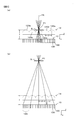
- FIG. 2 is a perspective view of the imaging unit 100.
- FIG. 2 is a cross-sectional view schematically showing a microlens array 12 and an image sensor 13.
- FIG. It is the schematic diagram which looked at the micro lens array 12 from the incident direction of subject light.
- the digital camera according to the present embodiment has a focal position desired by the user by numerical processing by using the fact that an image signal acquired by photographing through a microlens array has wavefront information such as depth information. Generate image data.
- the subject luminous flux incident through the photographing lens forms an image near the microlens array.
- the position at which the light beam forms an image according to the position of the subject differs in the optical axis direction of the photographing lens. Further, if the subject is a three-dimensional object, the subject light beam does not form an image on the same plane.
- the digital camera generates (synthesizes) an image that reproduces an image of a subject that is imaged at an imaging position in the optical axis direction desired by the user.
- this generated image is referred to as a target image.
- the target image appears as if the focal point of the imaging optical system is at the imaging position (not the actual imaging position but the position desired by the user). Therefore, in the following description, this imaging position is referred to as a focal position.
- the digital camera of the present embodiment is configured to generate a composite image having a resolution larger than the number of microlenses included in the microlens array as the image. That is, a plurality of imaging pixels (light receiving elements) that output image signals that are pixels of a composite image are provided corresponding to one microlens.
- the digital camera not only captures not only the image signal output from the imaging pixel corresponding to one microlens but also the imaging pixels corresponding to the surrounding microlens so that a composite image of the focal position selected by the user is obtained.
- a composite image signal corresponding to an imaging region for one pixel of the composite image is generated, and a composite image in which the focal position can be changed is created. Details will be described below.
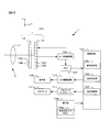
- FIG. 1 is a diagram showing a configuration of a digital camera according to the first embodiment.
- the digital camera 1 is configured such that the interchangeable lens 2 having the photographing lens L1 can be attached and detached by, for example, a bayonet type lens mount mechanism.
- the digital camera 1 includes an imaging unit 100, a control circuit 101, an A / D conversion circuit 102, a memory 103, an operation unit 108, a display 109, an LCD drive circuit 110, and a memory card interface 111.
- the imaging unit 100 includes a microlens array 12 and an imaging element 13 in which a large number of microlenses 120 are arranged two-dimensionally.
- the Z axis is set to be parallel to the optical axis of the photographic lens L1
- the X axis and the Y axis are set to be orthogonal to each other in a plane orthogonal to the Z axis.
- the photographing lens L1 is composed of a plurality of optical lens groups, and forms an image of a light beam from a subject near the focal plane.
- the taking lens L1 is represented by a single lens for convenience of explanation.
- the microlens array 12 and the image sensor 13 are arranged in order.
- the image sensor 13 is configured by a CCD or CMOS image sensor including a plurality of photoelectric conversion elements.
- the image sensor 13 captures a subject image formed on the imaging surface, and outputs a photoelectric conversion signal (image signal) corresponding to the subject image to the A / D conversion circuit 102 under the control of the control circuit 101.
- the details of the imaging unit 100 will be described later.
- the A / D conversion circuit 102 is a circuit that performs analog processing on the image signal output from the image sensor 13 and then converts it to a digital image signal.
- the control circuit 101 includes a CPU, a memory, and other peripheral circuits.
- the control circuit 101 reads and executes a control program stored in advance in a ROM (not shown) or the like. With this control program, the control circuit 101 performs a predetermined calculation using signals input from each unit constituting the digital camera 1 and sends a control signal to each unit of the digital camera 1 to control the photographing operation.
- the control circuit 101 determines the focus position of the target image based on the operation signal input from the operation unit 108 in response to the operation of the focus position input button 108a as will be described later.
- the control circuit 101 functionally includes an image composition unit 105, a composition determination unit 106, and a composition control unit 107.
- the image synthesis unit 105 synthesizes an image with an arbitrary focal plane different from the planned focal plane of the photographic lens L1.
- the composition determination unit 106 determines whether or not the focal position input from the operation unit 108 is within a predetermined range (described later) in which the resolution of the composite image is reduced.
- the composition control unit 107 controls the image composition unit 105 based on the determination of the composition determination unit 106 to create a composite image, and outputs a final image. Details of the image composition unit 105, composition determination unit 106, and composition control unit 107 will be described later.
- the memory 103 is used to temporarily store the image signal digitally converted by the A / D conversion circuit 102, and data during or after the image processing, image compression processing, and display image data creation processing. It is a volatile storage medium.
- the memory card interface 111 is an interface that allows the memory card 111a to be attached and detached.
- the memory card interface 111 is an interface circuit that writes image data to the memory card 111a and reads image data recorded on the memory card 111a in accordance with the control of the control circuit 101.
- the memory card 111a is a semiconductor memory card such as a compact flash (registered trademark) or an SD card.
- the LCD drive circuit 110 is a circuit that drives the display 109 based on a command from the control circuit 101.
- the display device 109 is composed of a liquid crystal panel or the like, and displays display data created by the control circuit 101 based on image data recorded on the memory card 111a in the reproduction mode.
- the display 109 displays a menu screen for setting various operations of the digital camera 1.
- the operation unit 108 receives a user operation and outputs various operation signals corresponding to the operation content to the control circuit 101.
- the operation unit 108 includes a focus position input button 108a, a power button, a release button, other setting menu display switching buttons, a setting menu determination button, and the like.
- the focus position input button 108a is operated by the user when inputting the focus position y of the composite image.
- the operation unit 108 outputs an operation signal including the focus position y to the control circuit 101.
- the imaging unit 100 includes a microlens array 12 and an imaging element 13.
- the microlens array 12 includes a plurality of microlenses 120 that are two-dimensionally arranged squarely on the XY plane.
- photoelectric conversion elements 130 (hereinafter referred to as imaging pixels 130) that receive light that has passed through each microlens 120 are two-dimensionally arranged in an arrangement pattern corresponding to the microlens 120.
- the image sensor 13 is arranged at a position away from the microlens array 12 by the focal length f of the microlens 120. That is, for each microlens 120, a plurality of imaging pixels 130 corresponding to the microlens 120 are provided at positions separated by the focal length f of the microlens 120.
- FIG. 2 illustrates only a part of the plurality of microlenses 120 provided in the microlens array 12 and the plurality of imaging pixels 130 provided in the imaging element 13.
- one microlens 120 is covered with about 100 image pickup pixels 130, and therefore the microlens array 12 is about 1 / 100th the number of microlenses of the image pickup pixels 130 included in the image pickup device 13. 120.
- the focal length f of the microlens 120 is about several hundred micrometers (about one hundredth of the focal length of the photographing lens L1).
- the so-called exit pupil position of the photographic lens L1 can be regarded as almost infinite for the microlens 120. That is, the position of the exit pupil of the photographic lens L1 and the imaging surface of the imaging element 13 can be optically conjugate.
- the F value of the microlens 120 and the F value of the photographing lens L1 are the same.
- the entire area of the imaging pixel 130 covered by the microlens 120 is a projection of the entire exit pupil of the photographing lens L1.
- the light intensity distribution at the position of the exit pupil of the photographing lens L1 of the image divided by the microlens 120 is shown.
- the control circuit 101 generates composite image data for an image at a position (+ 2f, ⁇ 2f) about twice the front and back of the focal length f of the microlens 120 and stores the two composite image data in the memory 103. To do.
- the image composition may be performed in a Fourier space obtained by Fourier transforming the image signal output from the image sensor 13.
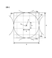
- FIG. 3 is a cross-sectional view schematically showing the microlens array 12 and the image sensor 13.
- the central microlens 120c and the composite pixel Px on the central axis CX of the microlens 120c among the composite pixels on the image plane S at a predetermined position will be considered.
- FIG. 3A shows a case where the image plane S to be synthesized is located near the apex of the microlens 120c.
- the image plane S to be synthesized when the image plane S to be synthesized is located at a position closer than the focal length f of the microlens 120c, the light beam constituting the synthesis pixel Px passes only through the microlens 120c, and the like.
- the microlenses 120a, 120b, 120d, and 120e are not reached.
- the light beam constituting the composite pixel Px is a plurality of microlenses. Is incident on.
- the focal length of the microlenses 120a to 120e is f
- the interval between the microlenses 120a to 120e is d
- the distance from the image surface to be synthesized to the apex of the microlenses 120a to 120e is f
- n is a dimensionless number that indicates how far the light beam is incident on the microlens 120 from the microlens 120c corresponding to the composite pixel Px
- the synthesized pixel at a position on the central axis CX of the microlens 120c and away from the apex of the microlens 120c by the distance y is obtained by integrating the outputs of the imaging pixels 130 at the positions satisfying the above equation (1). That is, if the light intensity at the position of the distance x (output of the imaging pixel 130) is I (x), the pixel value P of the composite pixel Px can be calculated by the following equation (2).
- x in the above equation (2) takes a value in a range corresponding to a plurality of microlenses, and to which microlens each value belongs is determined by the above equation (1).
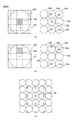
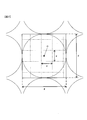
- FIG. 4 is a schematic view of the microlens array 12 as seen from the incident direction of the subject light.
- the pitch g of the grating 122 is determined by the position of the image to be synthesized (focal position y). For example, if the focal position y is four times the focal length f of the microlens 120, the pitch g of the grating 122 is a quarter of the distance d between the microlenses 120 as shown in FIG.
- the grid 122 represents which imaging pixel 130 is combined by integrating the output of one composite pixel Py corresponding to the center O of the micro lens 120j.
- the lattice 122 is configured by a total of 25 rectangular sections. This indicates that the synthesized pixel Py is synthesized by integrating the outputs of the imaging pixels 130 corresponding to each of these 25 sections.
- each section in the lattice 122 indicates which microlens 120 is covered by the microlens 120 around the microlens 120j.
- FIG. 5A An enlarged view of the microlens 120j is shown on the left side of FIG. 5A, and a microlens around the microlens 120j is shown on the right side of FIG. 5A.
- the section 140j corresponds to the imaging pixels 130j in a range corresponding to the section 140j in the lattice 122 among the imaging pixels 130 covered with the microlens 120j.
- a section 140g adjacent to the upper side of the section 140j is a section in the grid 122 among the imaging pixels 130 covered by the microlens 120g adjacent to the upper side of the microlens 120j.
- One composite pixel corresponding to the center O of the microlens 120j is obtained by integrating the outputs of the imaging pixels 130 in the 25 ranges thus specified. These 25 ranges are shown in FIG.
- the focal position y is four times the focal length f of the microlens 120
- one composite pixel corresponding to the center O of the microlens 120j is the microlens 120j and 24 surrounding microlenses 120.
- the output of the imaging pixels 130 covered by the image is integrated by integration, and the position of the imaging pixel 130 is as shown in FIG.
- N imaging pixels 130 covered by the microlens 120 there are N imaging pixels 130 covered by the microlens 120, and the coordinates of these imaging pixels 130 in the microlens 120 using i and j with reference to the center of the microlens 120.
- the integration for synthesizing is expressed by the following equations (3) to (7).
- the functions ⁇ x and ⁇ y in the equations (5) and (6) are determined by the division of the imaging surface of the imaging device 13 by the lattice 122 described above.
- the pitch g of the grating 122 decreases as the focal position y moves away from the apex of the microlens 120.
- the pitch g matches the distance d of the microlens 120.
- the above is the principle of creating a composite image in which one pixel is combined for each microlens 120.
- a synthesized pixel at a position corresponding to the center of the microlens 120 is synthesized.
- the resolution of the synthesized image is the microlens 120. It becomes equal to the number of. For example, if the number of imaging pixels 130 covered by the microlens 120 is 100, the resolving power is 1/100 of the original resolving power of the image sensor 13. If the image sensor 13 is an image sensor with 10 million pixels, the composite image has 100,000 pixels, and sufficient resolution cannot be obtained.
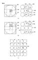
- a pixel of the composite image is set at a position other than the center of the microlens 120, and an integrated pattern of the imaging pixels 130 for combining the pixel is generated.
- the image synthesis unit 105 synthesizes a plurality of pixels for one microlens 120 by integrating the outputs of the imaging pixels 130 according to the integration pattern.
- the pitch g of the grating 122 represents (corresponds to) the focal position y. That is, the position of the composite pixel in the optical axis direction corresponds to the pitch g of the grating 122.
- the position in the direction perpendicular to the optical axis corresponds to the phase of the grating 122, and by changing the reference position of the grating 122, it is possible to synthesize synthesized pixels at positions other than the center of the microlens 120. It becomes.
- FIG. 7 is a diagram in which the lattice 122 is shifted to the right by a quarter of the pitch g.
- FIGS. 8A to 8C are obtained by shifting the grid 122 in this way and obtaining the integrated pattern in the same manner as FIGS. 5A to 5C.
- By integrating the outputs of the respective imaging pixels 130 shown in FIG. 8C it is possible to synthesize a synthesized pixel at a position shifted from the center O of the microlens 120 to the right by a quarter of the pitch g. .
- 16 synthesized pixels in the microlens 120 can be synthesized. That is, in principle, a composite image having the number of pixels obtained by multiplying the number of microlenses 120 by 16 can be obtained.
- the focal position y when a plurality of pixels are synthesized for each microlens 120 by the above-described method, sufficient resolving power may not be obtained depending on the focal position y.
- the focal length of the microlens 120 is f
- the resolving power is reduced in the range where the focal position y is + 2f to ⁇ 2f as compared with the case where the focal position y is placed outside this range. This is because when the focal position y is set at such a position, the above-described variation of the integrated pattern of the imaging pixels 130 is reduced, and some of them are the same.
- the focal position y is set in the range of + 2f to ⁇ 2f, some of the synthesized pixels are It will be the same output.
- the resolving power decreases as the focal position y is closer to the apex of the microlens 120.
- the image of the focal plane other than the set focal position y (hereinafter, the target image)
- the target image the image of the focal plane other than the set focal position y
- it is referred to as an auxiliary image
- the resolution of the target image is improved using this image.
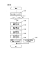
- FIG. 9 is a flowchart of the image composition process.
- the control circuit 101 executes this image composition processing by executing a predetermined control program.
- step S ⁇ b> 100 the composition control unit 107 receives the focal position y input from the operation unit 108.
- step S110 the composition determination unit 106 determines whether or not the input focal position y is between ⁇ 2f and + 2f. If the input focal position y is outside this range, the process proceeds to step S170, the composition control unit 107 controls the image composition unit 105, and the image composition unit 105 performs normal image composition by the above-described method. (Image synthesis for synthesizing a plurality of pixels per microlens 120) is performed, and a target image is output.
- the control circuit 101 stores the target image output from the synthesis control unit 107 in step S170, for example, in the memory card 111a or displays it on the display 109. On the other hand, if the composition determination unit 106 determines that the input focal position y is between ⁇ 2f and + 2f, the process proceeds to step S120.
- step S120 the composition control unit 107 controls the image composition unit 105 to cause the image composition unit 105 to compose the image at the focal position of ⁇ 2f (first auxiliary image).
- the auxiliary image corresponding to the position of ⁇ 2f synthesized here is referred to as P1.
- step S130 the composition control unit 107 controls the image composition unit 105 to cause the image composition unit 105 to compose an image (second auxiliary image) at the focal position of + 2f.
- the auxiliary image corresponding to the position of + 2f synthesized here is referred to as P2.
- the auxiliary images P1 and P2 are stored in the memory 103, respectively.
- this third auxiliary image is referred to as P0.
- the auxiliary image P0 is an image having a low spatial frequency that does not have the resolving power more than the number of the micro lenses 120.
- step S150 the composition control unit 107 controls the image composition unit 105, and causes the image composition unit 105 to perform normal image composition based on the focal position y input from the operation unit 108 in step S100.
- the target image synthesized here is referred to as P3. Since the target image P3 is a composite image of the image plane (focal plane) located in the range of ⁇ 2f to + 2f, the resolution is lost to some extent as described above.
- step S160 the composition control unit 107 performs the calculation shown in the following equation (8) for each pixel of the target image P3 synthesized in step S150, and creates and outputs the final target image P.
- P0 (i, j) represents a composite pixel at the coordinates (i, j) of the auxiliary image P0.
- P1 (i, j), P2 (i, j), and P3 (i, j) represent composite pixels of the coordinates (i, j) of the auxiliary image P1, the auxiliary image P2, and the target image P3, respectively.
- the first term on the right side of the above equation (8) represents the high frequency component of the spatial frequency obtained from the auxiliary image at the position of ⁇ 2f and the auxiliary image at the position of + 2f, and the composition control unit 107 determines this component.
- the final target image P is synthesized by adding to the target image P3 that has lost some resolution (the resolution of the target image P3 is increased).
- the digital camera 1 corresponds to each of the plurality of microlenses 120 arranged in a two-dimensional manner so that the subject light transmitted through the photographing lens L1 enters, and the microlens 120 corresponding to each of the plurality of microlenses 120. And a plurality of imaging pixels 130 that are disposed in the vicinity of the rear focal position and receive subject light transmitted through the microlens 120.
- the image synthesis unit 105 is configured to be able to synthesize an image having a focal plane different from the planned focal plane of the photographic lens L1 based on the outputs of the plurality of imaging pixels 130.
- the compositing control unit 107 is an image so that a target image that is an image of a focal plane near the vertices of the plurality of microlenses 120 and an auxiliary image that is an image of a focal plane other than the vicinity of the vertices of the plurality of microlenses 120 are combined.
- the synthesizer 105 is controlled to add the high frequency component of the auxiliary image to the target image and output it. Since it did in this way, a high resolution image can be synthesize
- the composition control unit 107 When a position that is not separated from the apexes of the plurality of microlenses 120 by more than twice the focal length f of the plurality of microlenses 120 is input as a focal plane, the composition control unit 107 outputs a high frequency component to the target image P3. to add. Since it did in this way, a high-resolution image can be synthesize
- auxiliary images P0 and P1 are images of focal planes at positions away from the apexes of the plurality of microlenses 120 by at least twice the focal length f of the plurality of microlenses 120. Since it did in this way, auxiliary image P0 and P1 become an image which contains a high frequency component reliably, and can add a high frequency component to the target image P3 reliably.
- the composition control unit 107 corresponds to mutually different focal planes (focal planes at positions away from the apexes of the plurality of microlenses 120 by two times the focal length f of the plurality of microlenses 120, respectively).
- the plurality of auxiliary images P1 and P2 are combined by the image combining unit 105, and the high frequency components of the plurality of auxiliary images P1 and P2 are added to the target image P3 and output. Since it did in this way, a high frequency component can be added more accurately.
- Modification 2 When performing image synthesis in real time according to the input of the focal position y and displaying a synthesized image, etc., a sequence of discrete focal positions is determined in advance in all possible focal position ranges, and image synthesis is performed in advance for these. You may keep going. For example, when the range of the focal position y is ⁇ 6 millimeters and the focal length f of the microlens 120 is 300 micrometers, 41 points of ⁇ 20f, ⁇ 19f,..., ⁇ f, 0, f, 2f,. Image synthesis is performed in advance and stored in the memory 103. By doing in this way, the processing load of the control circuit 101 at the time of displaying a composite image can be reduced.
- Mode 3 In the first embodiment, in order to increase the resolving power of the target image P3, high frequency components are extracted from the two auxiliary images P1 and P2 and added to the target image P3.
- the present invention is not limited to such an embodiment.
- the resolution of the target image P3 can be increased even when the high-frequency component is extracted only from the auxiliary image P1 and added to the target image P3.
- the auxiliary image P0 including only the low-frequency component is used.
- the high-frequency component from the auxiliary image P1 (and / or P2) is obtained by other methods. May be taken out.
- the positions of the focal planes of the auxiliary images P1 and P2 may be positions other than ⁇ 2f and + 2f, respectively.
- a high-frequency component to be added to the target image P3 can be extracted as long as it is at least twice the focal length f of the microlens 120 from the apex of the microlens 120.
- the arrangement of the microlenses 120 in the microlens array 12 is a square arrangement, but the present invention is not limited to such an arrangement.
- the microlenses 120 may be substantially hexagonal and arranged in a honeycomb shape.
- the present invention can be applied to an image processing apparatus that outputs a target image with high resolving power when an output signal from the imaging unit 100 is input.
- the image processing apparatus itself may not include the imaging unit 100.
- the output signal from the image pickup unit 100 (the output signal from the image pickup device 13) may be input by being stored in a portable storage medium such as a memory card or input via an electric communication line or the like. May be.
- the present invention is not limited to the above-described embodiments, and other forms conceivable within the scope of the technical idea of the present invention are also included in the scope of the present invention. .
Landscapes
- Engineering & Computer Science (AREA)
- Physics & Mathematics (AREA)
- General Physics & Mathematics (AREA)
- Theoretical Computer Science (AREA)
- Multimedia (AREA)
- Signal Processing (AREA)
- Optics & Photonics (AREA)
- Studio Devices (AREA)
- Image Processing (AREA)
Priority Applications (4)
| Application Number | Priority Date | Filing Date | Title |
|---|---|---|---|
| US14/380,802 US10587798B2 (en) | 2012-02-28 | 2013-02-25 | Image processing apparatus |
| EP13755116.4A EP2822266B1 (en) | 2012-02-28 | 2013-02-25 | Synthesis of an image at a plane in the vicinity of a microlens |
| CN201380010817.0A CN104137532B (zh) | 2012-02-28 | 2013-02-25 | 图像处理装置 |
| IN7183DEN2014 IN2014DN07183A (enExample) | 2012-02-28 | 2014-08-26 |
Applications Claiming Priority (2)
| Application Number | Priority Date | Filing Date | Title |
|---|---|---|---|
| JP2012041433A JP6102061B2 (ja) | 2012-02-28 | 2012-02-28 | 画像処理装置 |
| JP2012-041433 | 2012-02-28 |
Publications (1)
| Publication Number | Publication Date |
|---|---|
| WO2013129337A1 true WO2013129337A1 (ja) | 2013-09-06 |
Family
ID=49082534
Family Applications (1)
| Application Number | Title | Priority Date | Filing Date |
|---|---|---|---|
| PCT/JP2013/054819 Ceased WO2013129337A1 (ja) | 2012-02-28 | 2013-02-25 | 画像処理装置 |
Country Status (6)
| Country | Link |
|---|---|
| US (1) | US10587798B2 (enExample) |
| EP (1) | EP2822266B1 (enExample) |
| JP (1) | JP6102061B2 (enExample) |
| CN (2) | CN107888837B (enExample) |
| IN (1) | IN2014DN07183A (enExample) |
| WO (1) | WO2013129337A1 (enExample) |
Families Citing this family (3)
| Publication number | Priority date | Publication date | Assignee | Title |
|---|---|---|---|---|
| JP6185819B2 (ja) * | 2013-10-23 | 2017-08-23 | キヤノン株式会社 | 画像処理装置、画像処理方法およびプログラム |
| CN105812624B (zh) * | 2014-12-30 | 2019-01-11 | 深圳超多维科技有限公司 | 微透镜阵列成像装置 |
| CN106791498B (zh) * | 2016-11-18 | 2019-11-19 | 成都微晶景泰科技有限公司 | 图像定位方法、透镜阵列成像方法及装置 |
Citations (5)
| Publication number | Priority date | Publication date | Assignee | Title |
|---|---|---|---|---|
| JP2007004471A (ja) | 2005-06-23 | 2007-01-11 | Nikon Corp | 画像合成方法及び撮像装置 |
| US20070252047A1 (en) | 2006-04-28 | 2007-11-01 | Anadish Kumar Pal | Surface flow diverting and static charging ducted pores on wing or blade tip to reduce wake and BVI noise |
| JP2008294741A (ja) * | 2007-05-24 | 2008-12-04 | Olympus Corp | 撮像システム |
| JP2010114758A (ja) * | 2008-11-07 | 2010-05-20 | Nikon Corp | 画像合成装置および方法 |
| JP2011253431A (ja) * | 2010-06-03 | 2011-12-15 | Nikon Corp | 撮像装置 |
Family Cites Families (18)
| Publication number | Priority date | Publication date | Assignee | Title |
|---|---|---|---|---|
| US3017515A (en) * | 1959-10-26 | 1962-01-16 | Fairchild Camera Instr Co | Photoelectric unsharp-masking apparatus |
| JPS6053943B2 (ja) * | 1978-11-30 | 1985-11-28 | キヤノン株式会社 | カメラの合焦検出装置 |
| JPH04269750A (ja) * | 1990-12-05 | 1992-09-25 | American Teleph & Telegr Co <Att> | 離隔特徴をフォトレジスト層に印刷する方法 |
| US8005314B2 (en) * | 2005-12-09 | 2011-08-23 | Amnis Corporation | Extended depth of field imaging for high speed object analysis |
| JP4224996B2 (ja) * | 2002-07-25 | 2009-02-18 | パナソニック株式会社 | 撮像装置 |
| CN101313594A (zh) * | 2005-10-16 | 2008-11-26 | 米迪尔波得股份有限公司 | 用于增加数字图像捕获的质量的装置、系统和方法 |
| JP4157567B2 (ja) * | 2006-04-11 | 2008-10-01 | 株式会社東芝 | 動画像の高解像度化方法及び装置 |
| US8559705B2 (en) * | 2006-12-01 | 2013-10-15 | Lytro, Inc. | Interactive refocusing of electronic images |
| CN100585453C (zh) | 2007-02-09 | 2010-01-27 | 奥林巴斯映像株式会社 | 解码方法及解码装置 |
| JP2008275890A (ja) * | 2007-04-27 | 2008-11-13 | Olympus Imaging Corp | レンズ交換式デジタルカメラ |
| JP2009105717A (ja) | 2007-10-24 | 2009-05-14 | Sharp Corp | 撮像装置 |
| US7962033B2 (en) * | 2008-01-23 | 2011-06-14 | Adobe Systems Incorporated | Methods and apparatus for full-resolution light-field capture and rendering |
| JP4483951B2 (ja) * | 2008-01-28 | 2010-06-16 | ソニー株式会社 | 撮像装置 |
| US8824833B2 (en) | 2008-02-01 | 2014-09-02 | Omnivision Technologies, Inc. | Image data fusion systems and methods |
| JP4427097B2 (ja) * | 2008-06-18 | 2010-03-03 | パナソニック株式会社 | 画像処理装置、撮像装置、方法、およびプログラム |
| EP2403233B1 (en) * | 2008-10-10 | 2022-12-28 | Samsung Electronics Co., Ltd. | Image processing apparatus and method |
| KR101563729B1 (ko) * | 2008-10-10 | 2015-10-27 | 삼성전자주식회사 | 고해상도 영상을 생성하기 위한 영상 처리 장치 및 방법 |
| EP3798717B1 (en) * | 2012-02-16 | 2023-07-05 | University Of Washington Through Its Center For Commercialization | Extended depth of focus for high-resolution image scanning |
-
2012
- 2012-02-28 JP JP2012041433A patent/JP6102061B2/ja not_active Expired - Fee Related
-
2013
- 2013-02-25 CN CN201711407173.5A patent/CN107888837B/zh active Active
- 2013-02-25 CN CN201380010817.0A patent/CN104137532B/zh active Active
- 2013-02-25 EP EP13755116.4A patent/EP2822266B1/en active Active
- 2013-02-25 US US14/380,802 patent/US10587798B2/en active Active
- 2013-02-25 WO PCT/JP2013/054819 patent/WO2013129337A1/ja not_active Ceased
-
2014
- 2014-08-26 IN IN7183DEN2014 patent/IN2014DN07183A/en unknown
Patent Citations (5)
| Publication number | Priority date | Publication date | Assignee | Title |
|---|---|---|---|---|
| JP2007004471A (ja) | 2005-06-23 | 2007-01-11 | Nikon Corp | 画像合成方法及び撮像装置 |
| US20070252047A1 (en) | 2006-04-28 | 2007-11-01 | Anadish Kumar Pal | Surface flow diverting and static charging ducted pores on wing or blade tip to reduce wake and BVI noise |
| JP2008294741A (ja) * | 2007-05-24 | 2008-12-04 | Olympus Corp | 撮像システム |
| JP2010114758A (ja) * | 2008-11-07 | 2010-05-20 | Nikon Corp | 画像合成装置および方法 |
| JP2011253431A (ja) * | 2010-06-03 | 2011-12-15 | Nikon Corp | 撮像装置 |
Non-Patent Citations (2)
| Title |
|---|
| "Light Field Photography With a Handheld Plenoptic Camera", STANFORD TECH REPORT CTSR 2005-02 |
| See also references of EP2822266A4 |
Also Published As
| Publication number | Publication date |
|---|---|
| EP2822266A1 (en) | 2015-01-07 |
| CN104137532A (zh) | 2014-11-05 |
| EP2822266B1 (en) | 2017-08-02 |
| CN107888837B (zh) | 2020-03-27 |
| CN107888837A (zh) | 2018-04-06 |
| EP2822266A4 (en) | 2015-09-02 |
| US20150042838A1 (en) | 2015-02-12 |
| CN104137532B (zh) | 2018-01-26 |
| JP2013179424A (ja) | 2013-09-09 |
| IN2014DN07183A (enExample) | 2015-04-24 |
| US10587798B2 (en) | 2020-03-10 |
| JP6102061B2 (ja) | 2017-03-29 |
Similar Documents
| Publication | Publication Date | Title |
|---|---|---|
| JP6149339B2 (ja) | 表示装置 | |
| JP5671842B2 (ja) | 画像処理装置および撮像装置 | |
| JP5499778B2 (ja) | 撮像装置 | |
| JP4969474B2 (ja) | 復号方法、復号装置、及び復号プログラム | |
| JP6102061B2 (ja) | 画像処理装置 | |
| JP6036799B2 (ja) | 画像処理装置 | |
| JP6516045B2 (ja) | 画像処理装置 | |
| JP6376206B2 (ja) | 画像処理装置および撮像装置 | |
| JP6891935B2 (ja) | 画像表示装置 | |
| JP6502640B2 (ja) | 画像処理装置、画像処理方法、プログラム及び記録媒体 | |
| JP6600217B2 (ja) | 画像処理装置および画像処理方法、撮像装置およびその制御方法 | |
| JP6138222B2 (ja) | 画像処理装置、撮像装置、制御方法、及びプログラム | |
| JP2016082325A (ja) | 撮像装置、画像処理装置および画像処理プログラム | |
| JP2015207815A (ja) | 撮像素子および撮像素子を備えた撮像装置 | |
| JP2014110442A (ja) | 撮像装置 | |
| JP2019003665A (ja) | 画像処理装置 |
Legal Events
| Date | Code | Title | Description |
|---|---|---|---|
| 121 | Ep: the epo has been informed by wipo that ep was designated in this application |
Ref document number: 13755116 Country of ref document: EP Kind code of ref document: A1 |
|
| WWE | Wipo information: entry into national phase |
Ref document number: 14380802 Country of ref document: US |
|
| REEP | Request for entry into the european phase |
Ref document number: 2013755116 Country of ref document: EP |
|
| WWE | Wipo information: entry into national phase |
Ref document number: 2013755116 Country of ref document: EP |
|
| NENP | Non-entry into the national phase |
Ref country code: DE |