WO2013108508A1 - マンガン酸化物薄膜および酸化物積層体 - Google Patents
マンガン酸化物薄膜および酸化物積層体 Download PDFInfo
- Publication number
- WO2013108508A1 WO2013108508A1 PCT/JP2012/081760 JP2012081760W WO2013108508A1 WO 2013108508 A1 WO2013108508 A1 WO 2013108508A1 JP 2012081760 W JP2012081760 W JP 2012081760W WO 2013108508 A1 WO2013108508 A1 WO 2013108508A1
- Authority
- WO
- WIPO (PCT)
- Prior art keywords
- thin film
- oxide thin
- manganese oxide
- substrate
- strongly correlated
- Prior art date
- Legal status (The legal status is an assumption and is not a legal conclusion. Google has not performed a legal analysis and makes no representation as to the accuracy of the status listed.)
- Ceased
Links
Images



Classifications
-
- H—ELECTRICITY
- H10—SEMICONDUCTOR DEVICES; ELECTRIC SOLID-STATE DEVICES NOT OTHERWISE PROVIDED FOR
- H10N—ELECTRIC SOLID-STATE DEVICES NOT OTHERWISE PROVIDED FOR
- H10N99/00—Subject matter not provided for in other groups of this subclass
- H10N99/03—Devices using Mott metal-insulator transition, e.g. field-effect transistor-like devices
-
- C—CHEMISTRY; METALLURGY
- C01—INORGANIC CHEMISTRY
- C01G—COMPOUNDS CONTAINING METALS NOT COVERED BY SUBCLASSES C01D OR C01F
- C01G45/00—Compounds of manganese
- C01G45/12—Complex oxides containing manganese and at least one other metal element
- C01G45/1221—Manganates or manganites with trivalent manganese, tetravalent manganese or mixtures thereof
- C01G45/125—Manganates or manganites with trivalent manganese, tetravalent manganese or mixtures thereof of the type (MnO3)n-, e.g. CaMnO3
- C01G45/1264—Manganates or manganites with trivalent manganese, tetravalent manganese or mixtures thereof of the type (MnO3)n-, e.g. CaMnO3 containing rare earths, e.g. (La1-xCax)MnO3 or LaMnO3
-
- C—CHEMISTRY; METALLURGY
- C23—COATING METALLIC MATERIAL; COATING MATERIAL WITH METALLIC MATERIAL; CHEMICAL SURFACE TREATMENT; DIFFUSION TREATMENT OF METALLIC MATERIAL; COATING BY VACUUM EVAPORATION, BY SPUTTERING, BY ION IMPLANTATION OR BY CHEMICAL VAPOUR DEPOSITION, IN GENERAL; INHIBITING CORROSION OF METALLIC MATERIAL OR INCRUSTATION IN GENERAL
- C23C—COATING METALLIC MATERIAL; COATING MATERIAL WITH METALLIC MATERIAL; SURFACE TREATMENT OF METALLIC MATERIAL BY DIFFUSION INTO THE SURFACE, BY CHEMICAL CONVERSION OR SUBSTITUTION; COATING BY VACUUM EVAPORATION, BY SPUTTERING, BY ION IMPLANTATION OR BY CHEMICAL VAPOUR DEPOSITION, IN GENERAL
- C23C14/00—Coating by vacuum evaporation, by sputtering or by ion implantation of the coating forming material
- C23C14/06—Coating by vacuum evaporation, by sputtering or by ion implantation of the coating forming material characterised by the coating material
- C23C14/08—Oxides
- C23C14/083—Oxides of refractory metals or yttrium
-
- C—CHEMISTRY; METALLURGY
- C30—CRYSTAL GROWTH
- C30B—SINGLE-CRYSTAL GROWTH; UNIDIRECTIONAL SOLIDIFICATION OF EUTECTIC MATERIAL OR UNIDIRECTIONAL DEMIXING OF EUTECTOID MATERIAL; REFINING BY ZONE-MELTING OF MATERIAL; PRODUCTION OF A HOMOGENEOUS POLYCRYSTALLINE MATERIAL WITH DEFINED STRUCTURE; SINGLE CRYSTALS OR HOMOGENEOUS POLYCRYSTALLINE MATERIAL WITH DEFINED STRUCTURE; AFTER-TREATMENT OF SINGLE CRYSTALS OR A HOMOGENEOUS POLYCRYSTALLINE MATERIAL WITH DEFINED STRUCTURE; APPARATUS THEREFOR
- C30B23/00—Single-crystal growth by condensing evaporated or sublimed materials
- C30B23/02—Epitaxial-layer growth
-
- C—CHEMISTRY; METALLURGY
- C30—CRYSTAL GROWTH
- C30B—SINGLE-CRYSTAL GROWTH; UNIDIRECTIONAL SOLIDIFICATION OF EUTECTIC MATERIAL OR UNIDIRECTIONAL DEMIXING OF EUTECTOID MATERIAL; REFINING BY ZONE-MELTING OF MATERIAL; PRODUCTION OF A HOMOGENEOUS POLYCRYSTALLINE MATERIAL WITH DEFINED STRUCTURE; SINGLE CRYSTALS OR HOMOGENEOUS POLYCRYSTALLINE MATERIAL WITH DEFINED STRUCTURE; AFTER-TREATMENT OF SINGLE CRYSTALS OR A HOMOGENEOUS POLYCRYSTALLINE MATERIAL WITH DEFINED STRUCTURE; APPARATUS THEREFOR
- C30B29/00—Single crystals or homogeneous polycrystalline material with defined structure characterised by the material or by their shape
- C30B29/10—Inorganic compounds or compositions
- C30B29/16—Oxides
-
- C—CHEMISTRY; METALLURGY
- C30—CRYSTAL GROWTH
- C30B—SINGLE-CRYSTAL GROWTH; UNIDIRECTIONAL SOLIDIFICATION OF EUTECTIC MATERIAL OR UNIDIRECTIONAL DEMIXING OF EUTECTOID MATERIAL; REFINING BY ZONE-MELTING OF MATERIAL; PRODUCTION OF A HOMOGENEOUS POLYCRYSTALLINE MATERIAL WITH DEFINED STRUCTURE; SINGLE CRYSTALS OR HOMOGENEOUS POLYCRYSTALLINE MATERIAL WITH DEFINED STRUCTURE; AFTER-TREATMENT OF SINGLE CRYSTALS OR A HOMOGENEOUS POLYCRYSTALLINE MATERIAL WITH DEFINED STRUCTURE; APPARATUS THEREFOR
- C30B29/00—Single crystals or homogeneous polycrystalline material with defined structure characterised by the material or by their shape
- C30B29/10—Inorganic compounds or compositions
- C30B29/16—Oxides
- C30B29/22—Complex oxides
-
- C—CHEMISTRY; METALLURGY
- C30—CRYSTAL GROWTH
- C30B—SINGLE-CRYSTAL GROWTH; UNIDIRECTIONAL SOLIDIFICATION OF EUTECTIC MATERIAL OR UNIDIRECTIONAL DEMIXING OF EUTECTOID MATERIAL; REFINING BY ZONE-MELTING OF MATERIAL; PRODUCTION OF A HOMOGENEOUS POLYCRYSTALLINE MATERIAL WITH DEFINED STRUCTURE; SINGLE CRYSTALS OR HOMOGENEOUS POLYCRYSTALLINE MATERIAL WITH DEFINED STRUCTURE; AFTER-TREATMENT OF SINGLE CRYSTALS OR A HOMOGENEOUS POLYCRYSTALLINE MATERIAL WITH DEFINED STRUCTURE; APPARATUS THEREFOR
- C30B29/00—Single crystals or homogeneous polycrystalline material with defined structure characterised by the material or by their shape
- C30B29/60—Single crystals or homogeneous polycrystalline material with defined structure characterised by the material or by their shape characterised by shape
- C30B29/68—Crystals with laminate structure, e.g. "superlattices"
-
- H—ELECTRICITY
- H10—SEMICONDUCTOR DEVICES; ELECTRIC SOLID-STATE DEVICES NOT OTHERWISE PROVIDED FOR
- H10N—ELECTRIC SOLID-STATE DEVICES NOT OTHERWISE PROVIDED FOR
- H10N97/00—Electric solid-state thin-film or thick-film devices, not otherwise provided for
-
- H—ELECTRICITY
- H10—SEMICONDUCTOR DEVICES; ELECTRIC SOLID-STATE DEVICES NOT OTHERWISE PROVIDED FOR
- H10P—GENERIC PROCESSES OR APPARATUS FOR THE MANUFACTURE OR TREATMENT OF DEVICES COVERED BY CLASS H10
- H10P14/00—Formation of materials, e.g. in the shape of layers or pillars
- H10P14/60—Formation of materials, e.g. in the shape of layers or pillars of insulating materials
- H10P14/63—Formation of materials, e.g. in the shape of layers or pillars of insulating materials characterised by the formation processes
- H10P14/6326—Deposition processes
- H10P14/6328—Deposition from the gas or vapour phase
- H10P14/6329—Deposition from the gas or vapour phase using physical ablation of a target, e.g. physical vapour deposition or pulsed laser deposition
-
- H—ELECTRICITY
- H10—SEMICONDUCTOR DEVICES; ELECTRIC SOLID-STATE DEVICES NOT OTHERWISE PROVIDED FOR
- H10P—GENERIC PROCESSES OR APPARATUS FOR THE MANUFACTURE OR TREATMENT OF DEVICES COVERED BY CLASS H10
- H10P14/00—Formation of materials, e.g. in the shape of layers or pillars
- H10P14/60—Formation of materials, e.g. in the shape of layers or pillars of insulating materials
- H10P14/69—Inorganic materials
- H10P14/692—Inorganic materials composed of oxides, glassy oxides or oxide-based glasses
- H10P14/6938—Inorganic materials composed of oxides, glassy oxides or oxide-based glasses the material containing at least one metal element, e.g. metal oxides, metal oxynitrides or metal oxycarbides
- H10P14/6939—Inorganic materials composed of oxides, glassy oxides or oxide-based glasses the material containing at least one metal element, e.g. metal oxides, metal oxynitrides or metal oxycarbides characterised by the metal
-
- H—ELECTRICITY
- H10—SEMICONDUCTOR DEVICES; ELECTRIC SOLID-STATE DEVICES NOT OTHERWISE PROVIDED FOR
- H10P—GENERIC PROCESSES OR APPARATUS FOR THE MANUFACTURE OR TREATMENT OF DEVICES COVERED BY CLASS H10
- H10P14/00—Formation of materials, e.g. in the shape of layers or pillars
- H10P14/60—Formation of materials, e.g. in the shape of layers or pillars of insulating materials
- H10P14/69—Inorganic materials
- H10P14/692—Inorganic materials composed of oxides, glassy oxides or oxide-based glasses
- H10P14/6938—Inorganic materials composed of oxides, glassy oxides or oxide-based glasses the material containing at least one metal element, e.g. metal oxides, metal oxynitrides or metal oxycarbides
- H10P14/6939—Inorganic materials composed of oxides, glassy oxides or oxide-based glasses the material containing at least one metal element, e.g. metal oxides, metal oxynitrides or metal oxycarbides characterised by the metal
- H10P14/69396—Inorganic materials composed of oxides, glassy oxides or oxide-based glasses the material containing at least one metal element, e.g. metal oxides, metal oxynitrides or metal oxycarbides characterised by the metal the material containing at least one rare earth metal element, e.g. oxides of lanthanides, scandium or yttrium
-
- H—ELECTRICITY
- H10—SEMICONDUCTOR DEVICES; ELECTRIC SOLID-STATE DEVICES NOT OTHERWISE PROVIDED FOR
- H10P—GENERIC PROCESSES OR APPARATUS FOR THE MANUFACTURE OR TREATMENT OF DEVICES COVERED BY CLASS H10
- H10P14/00—Formation of materials, e.g. in the shape of layers or pillars
- H10P14/60—Formation of materials, e.g. in the shape of layers or pillars of insulating materials
- H10P14/69—Inorganic materials
- H10P14/692—Inorganic materials composed of oxides, glassy oxides or oxide-based glasses
- H10P14/6938—Inorganic materials composed of oxides, glassy oxides or oxide-based glasses the material containing at least one metal element, e.g. metal oxides, metal oxynitrides or metal oxycarbides
- H10P14/6939—Inorganic materials composed of oxides, glassy oxides or oxide-based glasses the material containing at least one metal element, e.g. metal oxides, metal oxynitrides or metal oxycarbides characterised by the metal
- H10P14/69397—Inorganic materials composed of oxides, glassy oxides or oxide-based glasses the material containing at least one metal element, e.g. metal oxides, metal oxynitrides or metal oxycarbides characterised by the metal the material containing two or more metal elements
-
- C—CHEMISTRY; METALLURGY
- C23—COATING METALLIC MATERIAL; COATING MATERIAL WITH METALLIC MATERIAL; CHEMICAL SURFACE TREATMENT; DIFFUSION TREATMENT OF METALLIC MATERIAL; COATING BY VACUUM EVAPORATION, BY SPUTTERING, BY ION IMPLANTATION OR BY CHEMICAL VAPOUR DEPOSITION, IN GENERAL; INHIBITING CORROSION OF METALLIC MATERIAL OR INCRUSTATION IN GENERAL
- C23C—COATING METALLIC MATERIAL; COATING MATERIAL WITH METALLIC MATERIAL; SURFACE TREATMENT OF METALLIC MATERIAL BY DIFFUSION INTO THE SURFACE, BY CHEMICAL CONVERSION OR SUBSTITUTION; COATING BY VACUUM EVAPORATION, BY SPUTTERING, BY ION IMPLANTATION OR BY CHEMICAL VAPOUR DEPOSITION, IN GENERAL
- C23C14/00—Coating by vacuum evaporation, by sputtering or by ion implantation of the coating forming material
- C23C14/22—Coating by vacuum evaporation, by sputtering or by ion implantation of the coating forming material characterised by the process of coating
- C23C14/24—Vacuum evaporation
- C23C14/28—Vacuum evaporation by wave energy or particle radiation
-
- H—ELECTRICITY
- H10—SEMICONDUCTOR DEVICES; ELECTRIC SOLID-STATE DEVICES NOT OTHERWISE PROVIDED FOR
- H10P—GENERIC PROCESSES OR APPARATUS FOR THE MANUFACTURE OR TREATMENT OF DEVICES COVERED BY CLASS H10
- H10P14/00—Formation of materials, e.g. in the shape of layers or pillars
- H10P14/20—Formation of materials, e.g. in the shape of layers or pillars of semiconductor materials
- H10P14/22—Formation of materials, e.g. in the shape of layers or pillars of semiconductor materials using physical deposition, e.g. vacuum deposition or sputtering
-
- H—ELECTRICITY
- H10—SEMICONDUCTOR DEVICES; ELECTRIC SOLID-STATE DEVICES NOT OTHERWISE PROVIDED FOR
- H10P—GENERIC PROCESSES OR APPARATUS FOR THE MANUFACTURE OR TREATMENT OF DEVICES COVERED BY CLASS H10
- H10P14/00—Formation of materials, e.g. in the shape of layers or pillars
- H10P14/20—Formation of materials, e.g. in the shape of layers or pillars of semiconductor materials
- H10P14/34—Deposited materials, e.g. layers
- H10P14/3402—Deposited materials, e.g. layers characterised by the chemical composition
- H10P14/3434—Deposited materials, e.g. layers characterised by the chemical composition being oxide semiconductor materials
Definitions
- the present invention relates to a manganese oxide thin film and an oxide laminate. More particularly, the present invention relates to manganese oxide thin films and oxide stacks which are switched by electrical, magnetic or optical property switching under control of temperature, electric field, magnetic field or light irradiation.
- Perovskite type manganese oxide is a representative example of strongly correlated electron materials, and in that electron system, a charge-ordered phase in which 3d electrons of manganese (Mn) are aligned by primary phase transition, an electron orbital It is known that an orbital-ordered phase in which is aligned is expressed.
- the electronic phase In the charge alignment phase and the orbital alignment phase, carriers are localized and the electrical resistance is high, and the electronic phase is an insulator phase. Also, the magnetic properties of this electronic phase are an antiferromagnetic phase due to super exchange interaction and double exchange interaction.
- the electronic states of the charge alignment phase and the orbital alignment phase should often be regarded as semiconductors. In the charge alignment phase and the orbital alignment phase, carriers are localized, but the electric resistance is lower than that of a so-called band insulator. However, here, by convention, the electronic phase of the charge alignment phase or the orbital alignment phase is expressed as an insulator phase. Conversely, when the electrical resistance is low and exhibits metallic behavior, the electron phase exhibits a ferromagnetic phase because the spins are aligned.
- the metal phase there are various definitions of the metal phase, but in this case, “the one whose sign of the temperature derivative of resistivity is positive” is expressed as the metal phase. In correspondence with this expression, the above-mentioned insulator phase is redefined as "the sign of the temperature derivative of resistivity is negative".
- any of the electronic phases such as charge and orbital ordered phase in which both charge alignment and orbital alignment are established
- electrostatic Phase and the orbital alignment phase any of the electronic phases
- charge and orbital ordered phase in which both charge alignment and orbital alignment are established
- phenomena that cause various switching functions to be observed are observed in the single crystal bulk material of the substance that can be taken (Patent Documents 1 to 3). These phenomena are typically observed as a huge change in electrical resistance or a transition between an antiferromagnetic phase and a ferromagnetic phase. For example, resistance changes by orders of magnitude due to the application of a magnetic field are well known as the giant magnetoresistance effect.
- the phenomenon that provides the switching function is a temperature range of room temperature (eg 300 K or more) Needs to be realized.
- the switching functions disclosed in the above Patent Documents 1 to 3 are all confirmed at a low temperature, for example, the liquid nitrogen temperature (77 K) or less.
- the chemical composition of the Perovskite-type manganese oxide in these disclosures is represented as ABO 3 , and the atomically laminated surface is a laminated body repeatedly laminated with an AO layer, a BO 2 layer, an AO layer,.
- the crystal structure of such a laminate is referred to as AO-BO 2 -AO.
- the A site is at the top
- the B site is at the body center
- manganese is arrange
- the temperature at which the switching phenomenon is observed in the Perovskite-type manganese oxide disclosed in each of the above documents 1 to 3 that is, the temperature at which the charge orbital order is expressed (hereinafter referred to as “expression temperature”) is lowered.
- expression temperature the temperature at which the charge orbital order is expressed
- the type of element or ion occupying the A site of the crystal structure of Perovskite is considered to be.
- the A site of the crystal structure of Perovskite is randomly occupied by a trivalent rare earth cation (hereinafter referred to as "R") and a divalent alkaline earth (“Ae”), and the randomness is The onset temperature is lowered as a cause.
- the transition temperature to the charge alignment phase is It is also known that can be raised to about 500K.
- a site ordering arranging ions occupying the A site regularly, as exemplified here, is referred to as “A site ordering”, and such a Perovskite-type manganese oxide in which such A site ordering is realized Is called A-site ordered Perovskite type manganese oxide.
- One class of materials exhibiting such high transition temperatures is characterized as comprising Ba (barium) as the alkaline earth Ae.
- Y yttrium
- Ho holmium
- Dy dysprosium
- Tb terbium
- Gd gadolinium
- Eu europium
- the above-mentioned switching phenomenon is realized after forming a Perovskite-type manganese oxide in a thin film form. It will be necessary. However, even when the thin film is formed on the (100) plane-oriented substrate, there is a problem that it is difficult to realize the switching function. The cause is that lattice deformation called Jahn-Teller mode required for phase transition to charge alignment phase or orbital alignment phase is suppressed due to in-plane four-fold symmetry. .
- Patent Document 4 discloses forming a thin film of Perovskite oxide using a (110) plane-oriented substrate. According to this disclosure, in the case where the in-plane four-fold symmetry is broken in the (110) plane-oriented substrate, shear deformation of the crystal lattice is permitted when the formed thin film switches. When this shear deformation occurs, the crystal lattice is oriented parallel to the substrate surface, and the charge alignment surface and the orbital alignment surface become nonparallel to the substrate surface. Further, Patent Document 5 discloses an example in which the above-mentioned A-site ordered Perovskite type manganese oxide is also thinned.
- JP-A-8-133894 Japanese Patent Application Laid-Open No. 10-255481 Japanese Patent Application Laid-Open No. 10-261291 Japanese Patent Application Publication No. 2005-213078 JP 2008-156188 A
- the A-site ordered perovskite-type manganese oxide has a problem that the degree of order of ions at the A-site greatly affects the temperature at which the switching phenomenon is realized, that is, the temperature at which charge orbital order is developed.
- the degree of order of A-site ions is reduced even if defects are introduced into the thin film to be formed or the composition of the thin film is slightly deviated. Have a concern.
- the thin film on the (110) plane-oriented substrate reported in Patent Document 4 has a problem that it does not contribute to the solution of any of the problems of the reduction in the degree of order and the reduction in the expression temperature.
- the present invention has been made in view of the above problems.
- the present invention creates a novel device by providing a manganese oxide thin film or oxide stack that realizes control of phase transition by any external stimulus (external field) at room temperature to realize a switching function.
- both cations of two kinds of cations ie, trivalent rare earth elements (R) and divalent alkaline earths (Ae such as Sr and Ba), are perfskite type Mn
- R trivalent rare earth elements
- Ae divalent alkaline earths
- the inventors of the present invention considered that the reason is that the oxide occupies an A site. Then, it is considered that the approach using the Perovskite-type Mn oxide in which two types of cations occupy the A site can not solve the above problem, and a method different from that is searched and a concrete means for solving the above problem is found.
- the present invention solves at least one of the above-mentioned problems on the basis of a completely new principle.
- it is formed on the surface of the substrate, and is represented by the composition formula RMnO 3 (wherein R is at least one trivalent rare earth element selected from lanthanoids).
- R is at least one trivalent rare earth element selected from lanthanoids.
- R is at least one trivalent rare earth element selected from lanthanoids.
- a manganese oxide thin film is provided which has two crystal axes which are not equivalent to each other in the in-plane direction of the substrate surface.
- two crystal axes which are not equivalent to each other mean two crystal axes which are asymmetric with respect to in-plane four-fold symmetry operation.
- the in-plane two axes are [010] and [001], but they are indistinguishable by in-plane four-fold symmetry operation, that is, 90-degree rotation. In such a case, it is assumed that the two crystal axes are equivalent.
- two in-plane axes are [-120] and [001]. These do not coincide due to the four-fold symmetry operation described above, and in such a case, the two crystal axes will be referred to as nonequivalent.
- the manganese oxide thin film in this aspect is a thin film made of perovskite type manganese oxide.
- the manganese oxide has a crystal lattice of the composition expressed as ABO 3.
- the crystal of the manganese oxide thin film in this aspect has Mn (manganese) at the B site and is equipped with an oxygen octahedron which surrounds the Mn, as in the case of the ordinary perovskite-type crystal.
- the A site is occupied only by the cation of the trivalent rare earth element (R). That is, unlike the above-described conventional one, divalent alkaline earth (Ae) is not disposed at the A site.
- a trivalent rare earth element that is typically a lanthanoid, that is, La (lanthanum), Ce (cerium), Pr (praseodymium), Nd (neodymium), Pm (promethium), Sm At least one element selected from the group consisting of Eu, Gd, Tb, Dy, Ho, Er (erbium), Tm (thulium), Yb (ytterbium) and Lu (lutetium).
- Patent Document 4 and Patent Document 5 are materials having Sr (Patent Document 4) and Ba (Patent Document 5) which are divalent alkaline earths (Ae) at the A site. It is.
- the atomic layer containing the element R and the atomic layer not containing Mn and the atomic layer containing Mn and not containing the element R are alternately arranged in the direction perpendicular to the substrate surface.
- the atomic layer containing the element R and not containing Mn is typically an RO layer, ie, a layer consisting of the elements R and O (oxygen).
- the atomic layer containing Mn and not containing the element R is typically a MnO 2 layer, ie, a layer consisting of Mn and O.
- the RO layer and the MnO 2 layer alternately stacked in the direction perpendicular to the substrate surface are considered to be charged to +1 and -1, respectively.
- a voltage or an electric field due to the charged polar surface is always applied.
- This type valence of each element, R represents a trivalent, O -2 valence and, Mn from the charge neutrality condition for RMnO 3 is because of a +3.
- the manganese oxide thin film of the above aspect has two crystal axes which are not equivalent to each other in the in-plane direction of the substrate surface. For this reason, the symmetry of the manganese oxide crystal in the plane of the substrate surface is lower than the four-fold symmetry, shear deformation is allowed, and a first-order phase transition becomes possible.
- the crystal lattice of the SmBaMn 2 O 6 thin film formed on the substrate has four-fold symmetry which does not allow shear deformation. It will have sex.
- the manganese oxide thin film of the above aspect has two crystal axes which are not equivalent to each other in the in-plane direction of the substrate surface, for example, four-fold symmetry such as (100) orientation. Does not contain manganese oxide thin film. Note that having two crystal axes non-equivalent to each other in the in-plane direction of the substrate surface means that there are not two crystal axes equivalent to each other in the in-plane direction of the substrate surface.
- the electronic phase of the manganese oxide which is the material of the thin film of the above aspect of the present invention exhibits the property of phase transition between an insulator and a metal by Mott transition.
- a manganese oxide is also a kind of substance group generally called Mott insulator.
- the manganese oxide thin film in the present application is a thin film which exhibits the property of causing metal-insulator transition, and is not always always the insulator phase.
- Such a material is hereinafter referred to as "manganese oxide”.
- not only temperature but also external stimuli hereinafter referred to as "external field" may be involved in Mott transition.
- the insulator phase appears on the low temperature side and the metal phase appears on the high temperature side.
- the insulator phase appears on the side where the external field is weak, and the metal phase appears on the side where the external field is strong.
- the transition temperature of the Mott transition which usually appears at a temperature higher than room temperature, is made lower than before, and the external field threshold for the Mott transition is made smaller than before. Means either or both.
- the external field here typically includes a magnetic field, an electric field, an electric current, light, and a pressure, and any combination thereof.
- the composition of the manganese oxide thin film has a composition formula RMnO 3 (where R is La, Ce, Pr, Nd, Pm, Sm, Eu, Gd, Tb, Dy)
- R is La, Ce, Pr, Nd, Pm, Sm, Eu, Gd, Tb, Dy
- the manganese oxide thin film of the above aspect is provided, which is represented by at least one selected trivalent rare earth element).
- the above group of trivalent rare earth elements is an element group in which lanthanoids are arranged in the order of atomic numbers and Ho and the like are excluded.
- the trivalent rare earth element is selected from the above group, it is possible to control the degree of rotation of the oxygen octahedron, and there is an advantage that it is possible to adjust the ease of occurrence of orbital alignment.
- the composition of the manganese oxide thin film has a composition formula RMnO 3 (where R is La, Ce, Pr, Nd, Pm, Sm, Eu, Gd, Tb, Dy)
- R is La, Ce, Pr, Nd, Pm, Sm, Eu, Gd, Tb, Dy
- the manganese oxide thin film of the above aspect is also provided, which is represented by at least two selected trivalent rare earth elements).
- Cations of the rare earth element R trivalent in the composition formula RMnO 3 manganese oxide thin film of the present invention need not necessarily be one element. That is, for example, when the chemical composition when two kinds of trivalent rare earth elements are used as the element R is expressed in another format, the composition expressed as RMnO 3 which is a manganese oxide of this embodiment is And a composition represented as (R 1 MnO 3 ) X (R 2 MnO 3 ) 1 -X , where 0 ⁇ X ⁇ 1, where R 1 and R 2 are separate rare earth elements that can be trivalent cations, respectively. Become.
- the composition represented in this manner typically has an arbitrary ratio X of the manganese oxide R 1 MnO 3 containing the rare earth element R 1 to the manganese oxide R 2 MnO 3 containing the rare earth element R 2 : It is a 1-X solid solution.
- the problem caused by the variation in the degree of order in the crystal of the manganese oxide thin film of the present embodiment is theoretically eliminated. This is because only the cation of the trivalent rare earth element described above is disposed at the A site.
- the trivalent rare earth element R is composed of a plurality of types having different ion radii.
- the effect appears in the rotation of the oxygen octahedron in the crystal structure, which leads to two effects.
- One is that it is possible to change the average lattice constant of the crystal lattice of manganese oxide formed in the thin film.
- the other is to introduce variation (randomness) in the angle of rotation of the oxygen octahedron of the crystal lattice of manganese oxide. Both of these act to reduce the external field threshold for Mott transfer. Therefore, using a plurality of rare earth elements R is a preferred embodiment.
- the trivalent rare earth element R is three or more. The details of these mechanisms will be described in the section "1-5 Two Effects of Multiple Elements R".
- the manganese according to the above embodiment wherein a cube root of a unit cell volume of a crystal lattice of a bulk material of the material forming the manganese oxide thin film is smaller than a lattice constant of a crystal lattice of the substrate.
- An oxide thin film is provided.
- the orbital alignment surface is disposed obliquely to the substrate surface, and the tensile strain acts on the manganese oxide thin film.
- the bond angle of Mn—O—Mn spreads and approaches 180 degrees. For this reason, carrier transfer in Mn—O—Mn is increased, and switching from the insulator phase to the metal phase by Mott transition is facilitated.
- an effect thereof for example, when an external field is used to cause Mott transition, it is possible to reduce the intensity of the external field required for Mott transition.
- the manganese oxide thin film of the above aspect wherein the plane orientation of the substrate is a (210) plane orientation.
- polarization in the in-plane [1-20] axis direction slightly inclined in the plane perpendicular direction occurs due to symmetry breaking. That is, in this embodiment, a voltage (electric field) inherently acts in the in-plane direction as well as in the in-plane direction, so that an anti-electric field due to polarization is also applied in the in-plane direction. The external field threshold for metal transfer is reduced.
- oxide stacks with additional layers added are provided in certain aspects of the invention. That is, in one aspect of the present invention, the manganese oxide thin film of any of the above aspects and a strongly correlated oxide thin film in contact with the manganese oxide thin film are provided, and the thickness of the entire oxide stack is obtained.
- An oxide laminate is provided which satisfies the relationship of tc and t1 ⁇ tc.
- the strongly correlated oxide thin film is disposed in contact with the manganese oxide thin film.
- the crystal structure of the material of the strongly correlated oxide thin film has a Perovskite structure expressed as ABO 3 similarly to the above-mentioned manganese oxide thin film.
- the A site is not necessarily occupied only by the trivalent rare earth element (R) cation.
- detection of the switching function of the manganese oxide thin film by insulator metal transition (Mott transition) is easier than that of the above-described manganese oxide thin film alone.
- the switching function of the manganese oxide thin film due to the insulator metal transition (Mott transition), that is, the change in the electronic state can be easily detected from the outside as, for example, the resistance change of the oxide laminate sample.
- the mechanism for facilitating the detection is called a dimensional crossover, and the details thereof will be described in the section "1-7 Improvement of detectability by layering (dimensional crossover)".
- the manganese oxide thin film of any of the above aspects a first strongly correlated oxide thin film in contact with one surface of the manganese oxide thin film, and the manganese oxide thin film A second strongly correlated oxide thin film in contact with the other surface of the second oxide film, the thickness t of the entire oxide stack, the thickness tm of the manganese oxide thin film, and the first and second strong
- Max () is a function that returns the maximum value of variables, and an oxide stack satisfying the relationship is also provided.
- the strongly correlated oxide thin film is disposed in contact with both surfaces of the manganese oxide thin film.
- the effect of bringing the strongly correlated oxide thin film into contact can be obtained more remarkably than in the case of only one side.
- the element at the A site is a rare earth element R having a uniform valence of +3, and an atomic layer containing the element R and no Mn. Since the atomic layers containing Mn and not containing the element R are alternately arranged in the direction perpendicular to the substrate surface, the influence of the variation of the order is basically eliminated, and the Mott transition controlled by the external field is It is realized at room temperature.
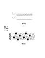
- FIG. 1 (a) is an overall view showing the configuration of a manganese oxide thin film formed on a substrate
- FIGS. 1 (b) and 1 (c) show atomic layered surfaces (cross-sectional views) of the manganese oxide thin film. It is an enlarged view which shows. It is explanatory drawing explaining the additional electric field which arises in the manganese oxide thin film in one Embodiment of this invention.
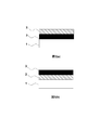
- FIGS. 2A and 2B are cross-sectional views similar to FIGS. 1A and 1B, respectively.
- FIG. 3 (a) is an example in which the strongly correlated oxide thin film is formed on the substrate side of the manganese oxide thin film
- FIG. 3 (b) is an example in which the strongly correlated oxide thin film is formed on the surface of the manganese oxide thin film is there.
- it is a schematic sectional view of an example of an oxide laminate formed by bringing a strongly correlated oxide thin film into contact with both sides of a manganese oxide thin film.
- FIG. 6 (a) shows a state in which the oxygen octahedron is deformed in the direction of rotation in the crystal lattice and the angle of Mn—O—Mn is smaller than 180 degrees
- FIG. 6 (b) is a stretching from the substrate. The strain shows that the oxygen octahedron is deformed in the direction of rotation in the crystal lattice, and the angle of Mn—O—Mn is expanded.
- the manganese oxide thin film of one embodiment of the present invention is a schematic diagram showing the difference of the strain of the oxygen octahedron in the crystal structure which arranged two kinds of lanthanoid elements R 1 and R 2 different from each other in ion radius at random.
- the element of the Pr site (A site) of PrMnO 3 is a lanthanoid such as La, Ce, Pr, Nd, Pm, Sm, Eu, Gd, Tb, Dy, Ho, Er, Tm, Yb, Lu
- a lanthanoid such as La, Ce, Pr, Nd, Pm, Sm, Eu, Gd, Tb, Dy, Ho, Er, Tm, Yb, Lu
- the oxygen octahedron has a strained structure of GdFeO 3 type, that is, in the crystal lattice, the lattice of the A site is not deformed, but the oxygen octahedron surrounding Mn is deformed. And the degree of deformation of the displacement or rotation increases in this order in the above replacement of the whole range from lanthanide La to Ho.
- the crystal structure tends to be more easily hexagonal than bulk orthorhombic because the ion radius is further reduced when replacing in the range from Er to Lu.
- the rhombic structure can be realized by epitaxial growth.
- FIG. 6 is an explanatory view showing the angle of Mn—O—Mn in the manganese oxide thin film of the present embodiment.
- FIG. 6 (a) shows a state in which the crystal lattice is deformed in the direction in which the oxygen octahedron rotates, and the angle of Mn—O—Mn is smaller than 180 degrees
- FIG. 6 (b) is a stretching from the substrate.
- the inventor of the present application realizes orbital alignment under the same physical mechanism in the range of La, Ce, Pr, Nd, Pm, Sm, Eu, Gd, Tb, and Dy excluding lanthanoid from Ho and the like. I think that is.
- the ease of occurrence of orbital alignment in this range exhibits systematic dependence on the ion radius as well as the antiferromagnetic transition temperature.
- a phenomenon observed in a strongly correlated electron system such as charge alignment or orbital alignment is not only a cooperative phenomenon but also an aspect of a many-body effect in a substance having a large electron correlation effect. That is, as long as only one unit cell containing only one Mn 3+ ion having 3d orbitals is targeted, the definition that charges and electron trajectories are aligned does not apply. Therefore, consider the electronic state in a system in which two unit cells are connected. In this case, the state (orbital state) of the electron orbit of one unit cell and the orbital state of the other unit cell are mutually competitive.
- the orbital alignment state is realized if the system is stable, and if the system is not aligned, the orbital alignment state is broken.
- the energy difference between these two states that is, the state in which the orbital alignment state is realized and the state in which it is collapsing, is to make the system of two unit cells stable in either state. It may be too small. Therefore, in the electronic state in a system in which two unit cells are connected, it can not be said that the orbital alignment is definite.
- N is an integer sufficiently larger than 2.
- N is an integer sufficiently larger than 2.
- all the trajectories contained in the N unit cells are aligned, as compared to the state in which the trajectory of only one of the N unit cells is different from the trajectory of the other N-1 unit cells.
- interactions from the surrounding N-1 unit cells act on the trajectory of one unit cell to align different trajectories.
- the orbits included in N unit cells It is more stable if everything is aligned.
- interactions between unit cell trajectories work to align the entire trajectories, and the entire system is stabilized.
- the Mott transition is a first-order phase transition (first-order transition).
- first-order transition the symmetry of the crystal that allows shear deformation is adopted so as not to disturb the transition of the yarn-Teller mode.
- a crystal structure of the manganese oxide thin film of the present embodiment a crystal structure of an atomic lamination surface in which an RO layer and an MnO 2 layer are alternately laminated in the direction perpendicular to the substrate surface, ie, RO-MnO.
- FIG. 1 is a schematic cross-sectional view of an example of a manganese oxide thin film having a structure of RMnO 3 in the present embodiment, and shows a cross-sectional view of a manganese oxide thin film formed on the surface of a (210) plane-oriented substrate.
- FIG. 1 (a) is an overall view showing the configuration of a manganese oxide thin film formed on a substrate
- FIG. 1 (b) is a cross-sectional view taken along a plane perpendicular to the [001] axis
- FIG. Shows a cross-sectional view in a plane perpendicular to the [1-20] axis.
- the crystal structures in FIGS. 1B and 1C are both of the manganese oxide thin film cut in a plane perpendicular to the substrate surface.
- FIGS. 1 (b) and 1 (c) illustrate the case where the crystal structure of the Perovskite structure shown by the composition formula of RMnO 3 of the manganese oxide thin film of the present embodiment takes cubic crystals. What is first understood from the crystal structure of the manganese oxide thin film of the present embodiment is that the two crystal axes in the substrate plane are not equivalent.
- the material of the manganese oxide thin film according to the present embodiment that is, the manganese oxide having a Perovskite structure and represented by the composition formula RMnO 3 has a crystal lattice other than cubic, that is, tetragonal or orthorhombic. It may be a Perovskite structure in a crystal structure having only lower order symmetry such as monoclinic (monoclinic), triclinic (triclinic), trigonal (trigonal) and hexagonal (hexagonal).
- the RO atomic layer and the MnO 2 atomic layer are alternately stacked and arranged as in the manganese oxide thin film of the present embodiment, and two crystal axes in the substrate plane are not If equivalent, the above-mentioned shear deformation is allowed.
- the substance of the crystal structure which can obtain the basic unit lattice of a crystal lattice only by connecting a plurality of the above-mentioned unit cells is included in the Perovskite structure of this embodiment, for example.
- the realization of the crystal structures shown in FIGS. 1 (b) and (c) can be confirmed by identifying crystal point groups by known X-ray diffraction.
- the alternate arrangement of RO atomic layers and MnO 2 atomic layers can be confirmed by direct observation of the atoms with STEM (scanning transmission electron microscope).
- the white arrows in the diagram of FIG. 1 (a) indicate the voltage (electric field) that inherently acts from this polar surface.
- the composition of the substrate 1 is expressed as ABO 3
- the surface of the substrate 1 on which the manganese oxide thin film 2 is formed is terminated by a BO 2 atomic layer, that is, when the surface of the substrate 1 is a BO 2 surface
- the manganese oxide thin film 2 is grown on the substrate 1.
- the first atomic layer from which the manganese oxide thin film 2 starts to grow becomes the RO layer, and in this case, the direction of the voltage (electric field) becomes the direction of the white arrow shown in FIG.
- the direction of the arrow is reversed.
- the polar surface is used as described above for the purpose of alternately laminating the atomic plane containing R and the atomic plane containing Mn in the direction perpendicular to the substrate surface as in RO-MnO 2 -RO-MnO 2- .
- one of the most typical of the polar surface is to adopt a substrate of (210) plane orientation as the substrate 1.
- the crystal structure shown in FIGS. 1B and 1C can be formed by coherently forming the crystal structure of the manganese oxide thin film of the composition formula RMnO 3 with respect to the crystal of the substrate 1. it can.
- FIG. 2 is an explanatory view for explaining an additional electric field in the present embodiment
- FIGS. 2 (a) and 2 (b) are cross-sectional views similar to FIGS. 1 (a) and 1 (b), respectively.
- Arrows attached to each of the elements R and Mn in the atomic stacking plane of FIG. 2B indicate directions of relative displacement of the positions of R and Mn in an actual crystal lattice.
- the 2A shows, as arrows shown in the manganese oxide thin film 2, a macroscopic polarization direction generated in the entire manganese oxide thin film 2 due to the above-mentioned polarization generated inside the manganese oxide.
- the macroscopic polarization can be generated by adopting the (210) plane-oriented substrate as the substrate 1. This is an effect which can not be obtained, for example, with a thin film on a (100) plane-oriented substrate whose plane is four-fold symmetric.
- the threshold of the external field required for the insulator-metal transition is further increased. It is expected to reduce.
- FIG. 5 is an explanatory view showing a state in which a track alignment surface indicated by a chain line is a (010) surface in the manganese oxide thin film of the present embodiment.
- the action of the substrate strain in this arrangement is an action such that the angle of Mn--O--Mn becomes closer to a straight line (180 degrees), that is, an action of widening the band width of carriers (electrons). This difference is shown in FIG. 6 (b) in comparison with that before the substrate strain (FIG. 6 (a)). As a result, the external field required for switching is reduced by the spread of the bandwidth.
- the element R is not only one of the elements selected from the group consisting of trivalent rare earth elements La, Ce, Pr, Nd, Pm, Sm, Eu, Gd, Tb, and Dy. And multiple types can be used.
- the composition expressed as RMnO 3 which is the manganese oxide of the above embodiment has R 1 and R each of different rare earth elements that can be trivalent cations.
- 2 also includes a composition expressed as (R 1 MnO 3 ) X (R 2 MnO 3 ) 1 -X (where 0 ⁇ X ⁇ 1).
- the composition according to this expression has an arbitrary ratio X: 1-X of manganese oxide R 1 MnO 3 containing rare earth element R 1 and manganese oxide R 2 MnO 3 containing rare earth element R 2.
- Solid solution of By employing a plurality of trivalent rare earth elements R, the ion radius of the cation disposed at the A site contained in the manganese oxide becomes a plurality of types. The effect appears in the rotation of the oxygen octahedron, leading to two effects.
- the first effect is the adjustment of the lattice constant of manganese oxide.
- the lattice constant of manganese oxide can be changed by the ratio of a plurality of rare earth elements R.
- the lattice constant of the manganese oxide of the composition formula (R 1 MnO 3 ) X (R 2 MnO 3 ) 1-X is, on average, a manganese oxide R 1 MnO 3 containing a rare earth element R 1 and a rare earth element R
- the lattice constant of each crystal lattice with manganese oxide R 2 MnO 3 containing 2 is weighted average by the ratio of the composition ratio X: 1-X.
- R 1 and R 2 are selected from La, Ce, Pr, Nd, Pm, Sm, Eu, Gd, Tb, and Dy from combinations having different ion radii.
- the lattice constant such as the cube root of the volume of the unit cell described above in the section of “1-4 Use of substrate distortion”.
- the lattice constant of the manganese oxide it becomes possible to determine the lattice constant of the manganese oxide as an average by the difference in the ion radius of plural kinds of elements R, and it is possible to adjust the strain received from the substrate 1 when the manganese oxide is thinned. It becomes.
- FIG. 7 is a schematic view showing a difference in strain of an oxygen octahedron in a crystal structure in which two kinds of lanthanoid elements R 1 and R 2 having different ion radii are randomly arranged in the manganese oxide thin film 2.
- the cation position is fixed to the cubic arrangement, and the oxygen position changes.
- the deformation of the Yarn-Teller mode is that of the oxygen octahedron surrounding Mn. Therefore, as shown by a chain line in FIG. 6, oxygen is arranged to be influenced by whether the adjacent lanthanoid is R 1 or R 2 . As a result, when carriers (electrons) pass through several crystal lattices, they are influenced by the angle of fluctuating Mn—O—Mn. The fluctuation leads to the reduction of the external field threshold for causing Mott transition. It supplements with two experimental facts that help to understand the relationship between this fluctuation and the Mott transition and theoretical explanations for each.
- the first experimental fact is about ordinary Perovskite manganese oxide in which atoms of A sites having different valences are randomly arranged.
- Perovskite manganese oxide having a composition of Pr 0.5 Ca 0.5 MnO 3 is a manganese oxide in which Pr of formal valence +3 and Ca of +2 randomly occupy an A site.
- this manganese oxide a charge having an arrangement on a so-called checkerboard in which trivalent Mn and tetravalent Mn in formal valences are alternately arranged in a crystal plane at 240 K or less, and the electron orbits are also aligned. An orbital alignment insulating phase is shown.
- the phenomenon related to manganese oxides exhibiting this charge orbital alignment insulating phase is that the randomness introduced to the B site by substitution of Mn 4 + with Cr 3 + interferes with the long distance order of the charge orbital alignment phase, and It has been described that the formation of a ferromagnetic metal phase in E.f. facilitates transition of the electron system to the metal phase.
- the second experimental fact is a phenomenon that is seen more directly when the randomness is lowered in the conventional A site order.
- Perovskite manganese oxide expressed as a composition formula Sm 0.5 Ba 0.5 MnO 3 has two known crystal structures. One has an A site order, and the other has no A site order.
- the connection of atomic layers in the former lattice structure is BaO 2 -MnO 2 -SmO 2 -MnO 2 -BaO 2 -MnO 2- .
- (Ba, Sm) O 2 is an atomic layer in which Ba and Sm randomly occupy the position of the A site. And, it is known that the temperature T OO at which the orbital order phase disappears is higher in the former having the A site order than in the latter having no A site order. This is the second experimental fact. This experimental fact means that the crystal structure that lowers the entropy of A site order directly enhances the order of the electron system. Conversely, it can be said that the randomness introduced into the A site has a direct effect of reducing the order of the electron system.
- the second effect that is, the rotation angle of the oxygen octahedron at the time of arranging plural kinds of rare earth elements R
- the effects of the introduced variability (randomness) can be predicted at least qualitatively. That is, by intentionally introducing variations in the crystal lattice, the external field threshold for causing Mott transition is reduced.
- the degree of reduction of the threshold is sufficiently observed, which can be said to be a degree that enhances practicability.
- the external field threshold of the Mott transition it is not necessarily essential to distinguish the first effect and the second effect. If you need experimental confirmation to distinguish the two effects, you can do the following experiment. For example, a manganese oxide containing one rare earth element (for example, Sm) selected to have the same lattice constant (average lattice constant) and a manganese oxide containing two kinds of rare earth elements (for example, Pr and Tb) make. Then, the transition temperature of the Mott transition and the external field threshold are compared. In this comparison, if the ratio of the two rare earth elements Pr and Tb is adjusted to match the lattice constant with that of one rare earth element Sm, the transition temperature and the threshold value decrease caused by the above comparison Can be determined as the contribution of the second effect.
- Sm rare earth element
- Pr and Tb two kinds of rare earth elements
- the elements of the La, Ce, Pr, Nd, Pm, Sm, Eu, Gd, Tb, and Dy groups have a stable valence of +3 except for Ce, and also for Ce, +3 Is one of the stable valences, and there is no difference in the possibility of taking an electron configuration as a trivalent cation.
- X is a composition represented by (R 1 MnO 3 ) X (R 2 MnO 3 ) 1-X , as long as the rare earth elements R 1 and R 2 are selected in the range of the above element group.
- the value of means that there is less restriction.
- the composition of the thin film of manganese oxide and the composition of the target material for forming the thin film are not have a direct effect due to the difference in the conventional charge or electron orbit where, for example, divalent cations influenced the A site order as the electron orbit. Also mean. From these properties, the purpose is to adjust the effect on the bandwidth which is caused by the difference in the ion radius and the distortion caused by the crystal structure as mentioned above, the matching of the lattice constant with the substrate 1 and the crystal such as introduction of randomness.
- the type of the rare earth elements R 1 and R 2 and the ratio X can be determined with the main aim of adjusting the geometrical properties of the lattice.
- any of the manganese oxide thin films provided in the present embodiment actually undergoes Mott transition can be detected by various measurement means. For example, if the transmittance or reflectance is measured by optical measurement, it is possible to measure the presence or absence of a transition as a change in electronic structure corresponding to the energy of probe light for measurement. Besides, it is possible to detect the realization of the Mott transition as any physical quantity such as magnetic characteristics, deformation, and electrical resistance. And, such a change as a physical quantity is not merely whether the Mott transition can be detected, but also provides material properties utilized as a switching function when the manganese oxide thin film of the present embodiment is applied to a device.
- a thin film formed in contact with the thin film of manganese oxide that is, a thin film of a strongly correlated oxide formed to be continuous to the thin film of manganese oxide
- This strongly correlated oxide thin film is a material different from the above-mentioned manganese oxide that undergoes Mott transition, and is a layer added to utilize dimensional crossover.
- the thin film in order to stabilize the metal phase or to realize a metal-insulator transition, it is desirable that the thin film be formed thicker than a certain degree. If the film thickness of the strongly correlated oxide thin film is too thin, it is difficult to realize a stable metal phase or metal-insulator transition.
- critical thickness a metallic phase is realized in the strongly correlated oxide or Metal-insulator transition is realized.
- critical film thickness can also be said to be the lower limit value of the film thickness of the strongly correlated oxide which is preferable because the above-mentioned metal phase is stably present or metal-insulator transition is developed.
- FIG. 3 is a schematic cross-sectional view showing a configuration of an example of an oxide laminate including a manganese oxide thin film produced by bringing the strongly correlated oxide thin film into contact according to the present embodiment.
- FIG. 3 (a) is an example in which the strongly correlated oxide thin film is formed on the substrate side of the manganese oxide thin film
- FIG. 3 (b) is an example in which the strongly correlated oxide thin film is formed on the surface of the manganese oxide thin film is there. If this oxide laminate first forms a strongly correlated metal thin film on the surface of the substrate and then forms a thin film of manganese oxide (FIG.
- the strongly correlated oxide is With the help of the thin film, detection by current is possible.
- the carrier of the Mott insulator also has the effect of increasing the current to enhance the detectability.
- FIG. 4 is a schematic cross-sectional view of an example of an oxide laminate formed by bringing a strongly correlated oxide thin film into contact with both surfaces of a manganese oxide thin film in the present embodiment.
- max () is a function that returns the maximum value of variables.
- Example 1 of the present embodiment is an oxide laminate manufactured in the configuration shown in FIG. 4 in which the first and second strongly correlated oxide thin films 31 and 32 are brought into contact with both surfaces of the manganese oxide thin film 2 respectively.
- TbMnO 3 as the manganese oxide thin film 2
- La 0.5 Sr 0.5 MnO 3 (hereinafter referred to as LSMO) as the first and second strongly correlated oxide thin films 31 and 32
- (LaAlO 3 ) as the substrate 1 0.3 (SrAl 0.5 Ta 0.5 O 3 ) 0.7
- LSAT (210) plane orientation substrates were respectively adopted.
- the LSAT (210) substrate had its surface terminated by B sites.
- the cubic root of the unit cell volume of the bulk material of TbMnO 3 which is the material of the manganese oxide thin film 2 is 0.3853 nm, which is smaller than the lattice constant of 0.387 nm of the LSAT of the substrate 1.
- the orbital alignment plane in 1 is the (010) plane, and it is expected that the tensile strain from the substrate 1 acts on the manganese oxide thin film 2.
- the first and second strongly correlated oxide thin films 31 and 32 are not La 0.7 Sr 0.3 MnO 3 having a composition similar to that of LSMO but having a maximum Curie temperature T c (370 K), Sr was increased to form an overdoped composition ratio LSMO. This is intended to increase the Curie temperature T c of the first and second strongly correlated oxide thin films 31 and 32 in consideration of carriers (electrons) supplied when the manganese oxide thin film 2 undergoes insulator-metal transition. It is a thing.
- the manganese oxide thin film 2 and the first and second strongly correlated oxide thin films 31 and 32 were all formed by laser ablation.
- a target material for each thin film a polycrystalline material of each material manufactured by a solid phase reaction method was used which was formed into a cylindrical shape of ⁇ 20 mm ⁇ 5 mm.
- the substrate was evacuated to 3 ⁇ 10 ⁇ 9 Torr (4 ⁇ 10 ⁇ 7 Pa) or less. Thereafter, 1 mTorr (0.133 Pa) of high purity oxygen gas was introduced, and the substrate was heated to a final temperature of 900.degree.
- a process of etching the surface with buffered hydrofluoric acid is performed in advance.
- a KrF excimer laser with a wavelength of 248 nm was irradiated to the target of LSMO through the laser light introduction port of the chamber to form only 15 atomic layers of LSMO as the first strongly correlated oxide thin film 31.
- the atomic layer here is such that one atomic layer has a (210) plane distance d (210).
- the control of the film thickness that is, the number of atomic layers is determined based on the relationship between the number of shots of the laser pulse and the number of atomic layers which have been studied in advance.
- TbMnO 3 is irradiated with the laser through the port in the same atmosphere to form a TbMnO 3 thin film which is the manganese oxide thin film 2 of only six atomic layers, and again using the target of LSMO. Only 15 atomic layers of LSMO were formed as the second strongly correlated oxide thin film 32.
- the thickness of each layer is 5 unit cells (about 2.6 nm) in thickness t1 of the first strongly correlated oxide thin film 31, 2 unit cells (about 1.1 nm) in thickness tm of the manganese oxide thin film 2, and the second The thickness t2 of the strongly correlated oxide thin film 32 is 5 unit cells (about 2.6 nm).
- the thickness t of the entire oxide stack is 6.3 nm.
- a 4-terminal electrode was formed on the oxide laminate including the manufactured manganese oxide thin film 2, and the magnetoresistance measurement was performed at room temperature (300 K).
- the magnetic field was adopted as the external field because measurement is easy.
- the resistance value of the sample in this measurement began to decrease by application of a magnetic field having a magnetic flux density of 4.2 T or more, and decreased to 10 k ⁇ under a magnetic field of 4.8 T. Thus, it was confirmed that a huge negative magnetoresistance effect could be obtained.
- the magnetic field was reduced again, the resistance became 10 M ⁇ or more again, and it became clear that the insulator-metal transition which is a Mott transition appears at room temperature in the manganese oxide thin film 2 contained in the oxide stack.
- the manganese oxide thin film 2 capable of realizing switching at room temperature is possible.
- Example 1 explained the example of the oxide layered product which made the strong correlation oxide thin film contact on both sides of the manganese oxide thin film. However, even if an oxide stack in which the strongly correlated oxide thin film is in contact with only one surface side of the manganese oxide thin film is used, dimensional crossover can be used. As an example for confirming this point, Example 2 of the present embodiment will be described in which an oxide laminate having a two-layer structure similar to that shown in FIG. 3A is employed. In Example 2, an LSAT (210) substrate is employed as the substrate 1, only 21 atomic layers of LSMO are formed as the strongly correlated oxide thin film 3, and 9 atomic layers of TbMnO 3 as the manganese oxide thin film 2 are further formed thereon. Only formed.
- the pretreatment method for determining the atomic layer terminating the surface of the substrate 1 in Example 2 and the method for forming each of the oxide laminate, ie, the manganese oxide thin film 2 and the strongly correlated oxide thin film 3 are all available. The same as in Example 1.
- a four-terminal electrode was formed on the sample produced as Example 2, and the in-plane resistance was measured under no magnetic field.
- the process of raising the temperature from a low temperature (liquid nitrogen temperature or less) first around 200 K Insulator metal transition was observed. This is due to the insulator-metal transition of LSMO which is the strongly correlated oxide thin film 3.
- the entire sample became an insulator in the temperature range (253 to 353 K) assumed for the operation of the electronic device including around room temperature (300 K). Therefore, when the magnetic resistance was measured at room temperature in the same manner as in Example 1, the sample of Example 2 showed a behavior of 1 k ⁇ in a magnetic field of 5 T of magnetic flux density and 100 k ⁇ in the absence of a magnetic field.
- Example 2 While the magnetoresistance effect at room temperature of Example 2 is lower in resistance under a magnetic field as compared with the sample of Example 1, it does not increase so much even when no magnetic field is applied, and the resistance change is 2 digits. Stayed within. Although this change in resistance is sufficiently detectable, it is desirably ideally larger.
- the inventors of the present invention speculate that the cause of the decrease in resistance change is the leakage current due to LSMO, which is the thick, strongly correlated oxide thin film 3.
- each thin film is reversed to form on the surface of the substrate as shown in FIG. 3 (b), that is, TbMnO 3 which is the manganese oxide thin film 2 is formed on the substrate 1 side and then the strongly correlated oxide is formed.
- TbMnO 3 which is the manganese oxide thin film 2 is formed on the substrate 1 side and then the strongly correlated oxide is formed.
- the same magnetoresistance effect was measured also in the sample in which the LSMO as the thin film 3 was formed.
- Example 3 Next, in Example 3, an experiment was conducted to confirm the cause of not obtaining a large magnetoresistance effect in the two-layer structure of Example 2.
- a sample in which the thickness of the entire oxide laminate of Example 2 was reduced was produced.
- One of the purposes of Example 3 may be that the leakage current is increased due to the thick LSMO which is the strongly correlated oxide thin film 3 because the resistance change is reduced in Example 2 , To confirm the guess.
- the sample of Example 3 only 15 atomic layers in which LSMO as the strongly correlated oxide thin film 3 was reduced from Example 2 were formed on the substrate 1 which is the LSAT (210) substrate, while manganese oxide was formed.
- the TbMnO 3 layer was thickened as the thin film 2 and only 12 atomic layers were formed. Then, unlike the second embodiment, in the sample of the third embodiment, the magnetoresistance effect is not observed at all even in the range of no magnetic field to a magnetic field of 5 T at room temperature. The cause is considered to be that the TbMnO 3 layer, which is a manganese oxide thin film, is thickened. Therefore, in the four-terminal measurement performed so far, the distance between the current application electrode pairs at both ends of the four electrodes arranged on a straight line spaced from each other, that is, the electrode distance, is 500 ⁇ m of Example 2. It was 5 ⁇ m.
- the resistance measurement was performed with the inner voltage measurement electrode pair. Then, it was confirmed that the resistance, which was 100 M ⁇ when 0.1 ⁇ A was applied, decreased to 1 k ⁇ when 40 ⁇ A was applied, and a resistance change of five digits or more occurred when the applied current was between 0.1 ⁇ A and 40 ⁇ A.
- a current and a magnetic field are simultaneously applied, when a magnetic field having a magnetic flux density of 5 T was applied when 6 ⁇ A was applied, it was found that the magnetoresistance effect was observed this time. Thus, it can be seen that the insulator-metal transition can be obtained at room temperature even by the application of multiple external fields.
- the present embodiment can also be practiced with the configuration of a manganese oxide thin film or an oxide laminate other than those specified and included in Examples 1 to 3.
- a manganese oxide thin film or an oxide laminate other than those specified and included in Examples 1 to 3.
- various cubic Perovskite substrates including the SrTiO 3 (210) substrate can be adopted as the substrate.
- Such an example is, for example, a solid solution of a composition such as Pr 1 -x Nd x MnO 3 (0 ⁇ x ⁇ 1), that is, a ratio of 1-x: x of PrMnO 3 and NdMnO 3 .
- PrMnO 3 and NdMnO 3 are all-solid solution which is a solid solution at an arbitrary ratio. For this reason, it is possible to adjust the composition ratio of the manganese oxide thin film by producing the target at a desired ratio in the same laser ablation as in each of the above-described embodiments.
- all of Examples 1 to 3 utilize the dimensional crossover by the configuration of the oxide laminate to facilitate the operation of detecting Mott transition from the outside.
- the switching function itself of controlling the Mott transition by an external field at room temperature is realized even when it is performed only with a manganese oxide thin film that is not a laminate.
- the present invention provides an external field application such as magnetic field, light, electricity, pressure and the like by providing a manganese oxide thin film or an oxide laminate realizing a switching function by realizing Mott transition controlled by an external field at room temperature. It is used as a device that uses the switching phenomenon by.
Landscapes
- Chemical & Material Sciences (AREA)
- Organic Chemistry (AREA)
- Engineering & Computer Science (AREA)
- Materials Engineering (AREA)
- Metallurgy (AREA)
- Crystallography & Structural Chemistry (AREA)
- Inorganic Chemistry (AREA)
- Life Sciences & Earth Sciences (AREA)
- General Life Sciences & Earth Sciences (AREA)
- Geology (AREA)
- Mechanical Engineering (AREA)
- Chemical Kinetics & Catalysis (AREA)
- Microelectronics & Electronic Packaging (AREA)
- Crystals, And After-Treatments Of Crystals (AREA)
- Physical Vapour Deposition (AREA)
- Inorganic Compounds Of Heavy Metals (AREA)
- Hall/Mr Elements (AREA)
- Physics & Mathematics (AREA)
- Optics & Photonics (AREA)
Abstract
Description
[1 基本原理]
[1-1 マンガン酸化物薄膜におけるモット転移の容易化]
以下、本発明に係るマンガン酸化物薄膜の実施形態を図面に基づいて説明する。まず、スイッチング機能を室温にて実現するための基本原理、すなわち、室温のマンガン酸化物薄膜を外場によりモット転移させるための基本原理を説明する。一般に、マンガン酸化物薄膜の軌道整列温度はAサイト秩序型Mn酸化物などと比較しても遥かに高い。例えばPrMnO3の軌道整列温度は1000K以上にもなる。つまり、例えば300K程度の室温におけるマンガン酸化物薄膜は、軌道整列状態となっている。これが重要な認識の一つ目である。
マンガン酸化物薄膜においてスイッチング機能を実現させるためには、スイッチング機能を実現させる外場の閾値を低減することに加え、モット転移が一次の相転移(一次転移)であることも考慮される。このため、本実施形態のマンガン酸化物には、ずり変形を許容する結晶の対称性が採用されて、ヤーン・テラーモードの転移の障害とならないようにされる。より具体的には、本実施形態のマンガン酸化物薄膜の結晶構造として、RO層とMnO2層とが交互に基板面直方向に積層されている原子積層面の結晶構造、すなわち、RO-MnO2-RO…と並ぶ結晶構造を採用することとする。図1は、本実施形態におけるRMnO3の構造を有するマンガン酸化物薄膜の一例の概略断面図であり、(210)面方位基板の面の上に形成されたマンガン酸化物薄膜の断面図を示す。図1(a)は、基板に形成されているマンガン酸化物薄膜の構成を示す全体図であり、図1(b)には[001]軸に垂直な面による断面図、図1(c)には[1-20]軸に垂直な面による断面図を示している。図1(b)および(c)の結晶構造は、ともに基板面に垂直な面にて切断したマンガン酸化物薄膜のものである。
図1(a)の図中の白抜き矢印はこの極性表面から内在的に作用する電圧(電場)を示している。基板1の組成をABO3と表現した場合、マンガン酸化物薄膜2が形成される基板1の表面がBO2原子層で終端されているとき、つまり、基板1の表面がBO2面であるときに、その基板1にマンガン酸化物薄膜2を成長させるとする。すると、マンガン酸化物薄膜2が成長し始める最初の原子層はRO層となるため、この場合には電圧(電場)の方向は図1(a)に示す白抜き矢印の向きとなる。同様に、基板1の表面がAO面で終端されている場合には、この矢印の向きは反転した向きとなる。なお、基板1の表面をどちらで終端するかを造り分けることは特に困難性はない。
本実施形態においては、マンガン酸化物薄膜2が基板1から受ける歪を活用することにより、金属相に転移させやすくすることが可能である。このメカニズムには、マンガン酸化物すなわちRMnO3の組成により表されるモット絶縁体におけるMnを囲む酸素八面体の配置が関連している。上述したように、酸素八面体は、GdFeO3タイプの歪み構造(傾斜変位または回転の変形)を伴う。しかし、酸素八面体の変形は、基板歪に起因する伸張歪を、マンガン酸化物薄膜2のマンガン酸化物に与えることにより小さくすることが可能である。この変形を減少させるには、モット転移を起こすマンガン酸化物のバルク物質における単位胞体積の三乗根を、基板1の格子定数よりも小さくするようなマンガン酸化物と基板1とのそれぞれの具体的組成の組み合わせを選択すればよい。すると軌道整列面が(010)面となる配置、すなわち基板面に対して約45度傾斜した配置となる。図5は本実施形態のマンガン酸化物薄膜において、鎖線で示す軌道整列面が(010)面となっている状態を示す説明図である。この配置における基板歪の作用は、Mn-O-Mnの角度がより直線(180度)に近づくような作用、つまり、キャリア(電子)のバンド幅(band width)を広げる作用となる。この違いは、基板歪みが作用する前(図6(a))に対比させて図6(b)に示している。その結果、そのバンド幅の広がりの分だけスイッチングに必要となる外場が低減されるのである。
上述したように元素Rは、3価の希土類元素であるLa、Ce、Pr、Nd、Pm、Sm、Eu、Gd、Tb、Dyからなる群から選択される元素のうち、1種のみならず、複数種を用いることができる。例えばRとして2種の3価の希土類元素が用いられるときには、上記態様のマンガン酸化物であるRMnO3と表現される組成物は、3価のカチオンとなりうる別々の希土類元素それぞれをR1、R2として、(R1MnO3)X(R2MnO3)1-X(ただし、0<X<1)と表現される組成物も含んでいる。この表現による組成物は、上述したように、希土類元素R1を含むマンガン酸化物R1MnO3と、希土類元素R2を含むマンガン酸化物R2MnO3との任意の比率X:1-Xの固溶体である。複数種の3価の希土類元素Rを採用することにより、マンガン酸化物に含まれるAサイトに配置されるカチオンのイオン半径が複数種類のものとなる。その影響は酸素八面体の回転に現われ、結果として二つの効果を導く。
第1の効果はマンガン酸化物の格子定数の調整である。端的には、マンガン酸化物の格子定数を、複数種の希土類元素Rの比率によって変更しうること、ともいえる。組成式(R1MnO3)X(R2MnO3)1-Xのマンガン酸化物の格子定数は、平均的には、希土類元素R1を含むマンガン酸化物R1MnO3と、希土類元素R2を含むマンガン酸化物R2MnO3とのそれぞれの結晶格子の格子定数を、組成比X:1-Xの比率により加重平均したものとなる。この際、R1とR2は、La、Ce、Pr、Nd、Pm、Sm、Eu、Gd、Tb、Dyのうちから、イオン半径が互いに異なる組合せから選択される。これにより、「1-4 基板歪みの活用」の欄にて上述した単位胞の体積の三乗根といった格子定数を、平均として調整することができる。このように複数種の元素Rのイオン半径の違いが平均としてマンガン酸化物の格子定数を決定することが可能となり、マンガン酸化物を薄膜化した場合に基板1から受ける歪みを調整することが可能となる。その結果、GdFeO3タイプの傾斜変位または回転の変形において、酸素八面体の変形を減少させることが可能となる。つまり、Mn-O-Mnの角度に影響を及ぼす基板歪の作用を、複数種の希土類元素Rを採用することにより変更し、結果として、モット転移を生じさせるための外場閾値を低減することが可能となる。
第2の効果は、複数種の希土類元素Rを配置した際に、結晶格子内の位置によって、酸素八面体の回転角がばらつく現象に起因する効果である。いわば、結晶格子に意図的にばらつきを導入するために複数種の希土類元素Rを配置するのである。図7は、マンガン酸化物薄膜2において、互いにイオン半径の異なる2種類のランタノイド元素R1と元素R2をランダムに配置した結晶構造における酸素八面体の歪の違いを示す概略図である。ここでは、簡単のため、カチオン位置を立方晶の配置に固定した場合を仮定し、酸素位置が変化する様子を示している。ヤーン・テラーモードの変形は、Mnを囲む酸素八面体の変形である。そのため、図6に鎖線によって示したように、酸素が、近接しているランタノイドがR1であるかR2であるかの影響を受ける配置となる。その結果、キャリア(電子)がいくつもの結晶格子を通過する際に、揺らぎのあるMn-O-Mnの角度の影響を受けることとなる。その揺らぎは、モット転移を生じさせるための外場閾値を低減させることに繋がる。この揺らぎとモット転移との関係の理解を助ける二つの実験事実とそれぞれに対する理論的説明について補足する。
第1の実験事実は、価数が異なるAサイトの原子がランダムに配置した通常のぺロフスカイトマンガン酸化物についてのものである。Pr0.5Ca0.5MnO3の組成をもつペロフスカイトマンガン酸化物は、形式価数が+3のPrと+2のCaがランダムにAサイトを占めるマンガン酸化物である。このマンガン酸化物は、240K以下において、形式価数が3価のMnと4価のMnが、ある結晶面内で交互に並んだいわばチェッカーボード上の配列をとり、さらに電子軌道も揃った電荷軌道整列絶縁相を示す。ただし、温度を上昇させれば、常磁性絶縁相へと転移する。この物質において、形式価数が+4のMnを、形式価数3価が化学的に安定なCrにより置換すると、電荷軌道整列絶縁相が壊れやすくなり金属相が発現しやすくなるという実験事実が知られている。これが第1の実験事実である。Mn位置にランダムに置換した3価のCrは、サイトが固定した4価のMnと見なすことができる。この電荷軌道整列絶縁相を示すマンガン酸化物に関する現象は、Mn4+のCr3+への置換によりBサイトに導入されたランダムネスが電荷軌道整列相の長距離秩序を妨げるとともに、電荷軌道整列相内における強磁性金属相を生成し電子系の金属相への転移を容易化したため、と説明されている。
第2の実験事実は、より直接的に、従来のAサイト秩序において、ランダムネスが低下した場合に見られる現象である。組成式Sm0.5Ba0.5MnO3として表現されるペロフスカイトマンガン酸化物は、結晶構造に二種類のものが知られている。一つは、Aサイト秩序を有しているものであり、もう一つは、Aサイト秩序が無いものである。(100)配向している結晶系では、前者の格子構造における原子層の連なりは、BaO2-MnO2-SmO2-MnO2-BaO2-MnO2-…となる。これに対して後者では、(Ba、Sm)O2-MnO2-(Ba、Sm)O2-…となる。なお、(Ba、Sm)O2は、BaとSmとが、ランダムにAサイトの位置を占める原子層である。そして、Aサイト秩序を有している前者では、Aサイト秩序を有していない後者に比べて軌道秩序相が消失する温度TOOが高くなることが知られている。これが第2の実験事実である。この実験事実は、Aサイト秩序というエントロピーを低下させる結晶構造が、直接的に、電子系の秩序を高めることを意味している。その逆に、Aサイトに導入されるランダムネスは、電子系の秩序を低下させる直接的な効果を有している、ともいえる。
そして、上記第1および第2の実験事実と、それらをサポートする理論的説明に基づけば、上記第2の効果、すなわち、複数種の希土類元素Rを配置した際の酸素八面体の回転角に導入されるばらつき(ランダムネス)の効果を、少なくとも定性的には予測することができる。つまり、結晶格子に意図的にばらつきを導入することにより、モット転移を生じさせるための外場閾値は低減される。特に、Mn-O-Mnの角度とキャリアの伝導バンドのバンド幅との強い関係を考慮すれば、その閾値の低減の程度も十分に観測され、実用性を高める程度のものといえる。
重要なことに、La、Ce、Pr、Nd、Pm、Sm、Eu、Gd、Tb、Dyの元素群の各元素は、Ceを除き安定価数が+3であり、また、Ceについても、+3は安定な価数のひとつであり、3価カチオンとしての電子配置を取りうることには違いはない。このことは、一つには、上記元素群の範囲で希土類元素R1、R2を選択する限り、(R1MnO3)X(R2MnO3)1-Xと表現される組成のXの値には制限が少ないことを意味している。これは、マンガン酸化物の薄膜の組成についても、その薄膜を形成するためのターゲット材の組成についても成り立つ。もう一つ、マンガン酸化物の電子系の性質については、電子軌道として、例えば2価カチオンがAサイト秩序に影響した従来のような電荷や電子軌道の違いに起因する直接の効果は生じないことも意味している。これらの性質から、上述したイオン半径の違いとそれによる結晶構造に生じる歪みに原因を有するバンド幅への作用を調整する目的や、基板1との格子定数のマッチング、そしてランダムネスの導入といった結晶格子の幾何学的性質を調整すること主眼として、上記希土類元素R1、R2の種類や上記比率Xを決定することができる。もちろん、この事情は、希土類元素Rが2種のみの場合には限られず、La、Ce、Pr、Nd、Pm、Sm、Eu、Gd、Tb、Dyに含まれるすべての元素Rの2種以上の任意の組合せに対しても同様である。
本実施形態において提供されるいずれかのマンガン酸化物薄膜が実際にモット転移しているかどうかは、種々の測定手段によって検出することが可能である。例えば、光学的測定によって、透過率または反射率を測定すれば、測定のためのプローブ光のエネルギーに対応する電子構造の変化として、転移の有無を測定することが可能である。その他、磁気特性、変形、電気抵抗といった任意の物理量としてモット転移の実現を検知することが可能である。そして、そのような物理量としての変化は、単にモット転移を検知できるかどうかではなく、本実施形態のマンガン酸化物薄膜をデバイスに適用する際にスイッチング機能として活用される材料特性も提供する。
ただし、マンガン酸化物などのモット絶縁体を上記のように薄膜に形成すると、その材質特性の変化を外部から検知しにくい場合がある。この問題は必ずしも常に生じるとはいえない。もしその問題が、電気的な性質を反映する電子の伝導度に表われるドルーデ(Drude)成分、つまり直流抵抗の成分に関連して生じることがあるならば、それは系の低次元性(薄膜の場合は二次元性)に起因しキャリア(電子)が局在化するような場合であるといえる。例えば、薄膜の場合には、二次元の領域の一部において電子が局在化し伝導性を低下させることが起こりうる。この問題への対策として、本実施形態においては、次元クロスオーバー(dimension crossover)という仕掛けを利用することが好ましい。
t=tm+t1>tc、かつt1<tc
を満たすものとする。例えば、強相関酸化物薄膜の臨界膜厚tc(室温で金属相となるものとする)としては強磁性金属であるLa0.7Sr0.3MnO3薄膜を用いた場合、(210)面方位基板上では、8単位胞(約4nm)となる。
t=tm+t1+t2>tc、かつ、max(t1、t2)<tc
の関係を満たすものとする。ただし、max()は、変数のうちの最大値を返す関数である。このようにマンガン酸化物薄膜の両面に酸化物積層体を接触させて形成すると、上記次元クロスオーバーの効果がより効果的に発揮される。つまりマンガン酸化物薄膜の厚みtmを、片側のみに強相関酸化物薄膜を配置する場合よりも一層薄くてもよいこととなる。こうしてより弱い外場によるスイッチングが実現される。
次に、本実施形態をより具体的な実施例に基づいて説明する。以下の実施例に示す材料、使用量、割合、処理内容、処理手順、要素または部材の向きや具体的配置、そして測定のために採用する外場等は本発明の趣旨を逸脱しない限り適宜変更することかできる。したがって、本発明の範囲は以下の具体例に限定されるものではない。また、引き続き図3および図4を参照して説明する。
本実施形態の実施例1は、マンガン酸化物薄膜2の両面に、それぞれ第1および第2の強相関酸化物薄膜31、32を接触させた図4に示す構成に作製された酸化物積層体の実施例である。マンガン酸化物薄膜2としてTbMnO3、第1および第2の強相関酸化物薄膜31、32としてLa0.5Sr0.5MnO3(以下、LSMOと表記する)、基板1として(LaAlO3)0.3(SrAl0.5Ta0.5O3)0.7(以下LSATと表記する)(210)面方位基板をそれぞれ採用した。このLSAT(210)基板は、表面がBサイトにより終端されるものとした。なお、マンガン酸化物薄膜2の材質であるTbMnO3のバルク物質での単位胞体積の三乗根は0.3853nmであり、基板1のLSATの格子定数0.387nmよりも小さいことから、実施例1における軌道整列面は(010)面となり、マンガン酸化物薄膜2に対しては、基板1からの伸張歪が作用することが期待される。
また、第1および第2の強相関酸化物薄膜31、32は、LSMOと類似の組成でキュリー温度Tcが最大(370K)となる組成のLa0.7Sr0.3MnO3ではなく、Srを増大させてオーバードープされた組成比のLSMOとした。これは、マンガン酸化物薄膜2が絶縁体金属転移した際に供給されるキャリア(電子)を考慮に入れ第1および第2の強相関酸化物薄膜31、32のキュリー温度Tcを高める意図によるものである。
実施例1ではマンガン酸化物薄膜の両面に強相関酸化物薄膜を接触させた酸化物積層体の例を説明した。しかし、マンガン酸化物薄膜の一方の面側のみに強相関酸化物薄膜を接触させた酸化物積層体を採用しても次元クロスオーバーを利用することができる。この点を確認するための実施例として、図3(a)に示したものと同様の2層構造の酸化物積層体を採用した本実施形態の実施例2を説明する。実施例2においては、基板1としてLSAT(210)基板を採用し、強相関酸化物薄膜3としてLSMOを21原子層だけ形成し、さらにその上にマンガン酸化物薄膜2としてTbMnO3を9原子層だけ形成した。実施例2における基板1の表面を終端する原子層を決定するための事前処理方法、および、酸化物積層体つまりマンガン酸化物薄膜2および強相関酸化物薄膜3の各々の形成方法は、いずれも実施例1と同様とした。
次に、実施例3として、実施例2の2層構造では大きな磁気抵抗効果が得られない原因を確認する実験を行なった。実施例3においては、実施例2の酸化物積層体全体の厚みを減らした試料を作製した。実施例3の目的の一つは、実施例2において抵抗変化が小さくなった原因が、強相関酸化物薄膜3であるLSMOが厚いことに起因して漏れ電流が大きくなっているためではないか、という推測を確認するためである。具体的には、実施例3の試料は、LSAT(210)基板である基板1上に、強相関酸化物薄膜3としてLSMOを、実施例2より減らした15原子層だけ形成した一方、マンガン酸化物薄膜2としてTbMnO3層を厚くし12原子層だけ形成した。すると、実施例2とは異なり、実施例3の試料においては、室温では、無磁場から5Tの磁場の範囲においても全く磁気抵抗効果は見られなくなった。その原因は、マンガン酸化物薄膜であるTbMnO3層が厚くなったためと考えられる。そこで、これまで行っていた4端子測定において、互いに間を置いて直線上に並べられる4つの電極のうち、両端の電流印加用電極対の間の距離つまり電極間隔を、実施例2の500μmから5μmとした。そして、マンガン酸化物薄膜2に印加する電流値を制御しながら、内側の電圧測定用電極対により抵抗測定を行った。すると、0.1μA印加時に100MΩであった抵抗が、40μA印加時には1kΩにまで減少し、印加電流が0.1μAと40μAの間において5桁以上の抵抗変化が生じることが確認された。また、電流と磁場を同時に作用させる測定として、6μA印加時に磁束密度5Tの磁場を印加したところ、今度は磁気抵抗効果が観測されることが判明した。このように、複数の外場の印加によっても室温で絶縁体金属転移が得られることがわかる。
本実施形態は、実施例1~3を含め明示したもの以外のマンガン酸化物薄膜や酸化物積層体の構成によっても実施することは可能である。例えば基板としては、LSAT(210)基板(実施例1~3)以外にも、SrTiO3(210)基板をはじめとして様々な立方晶ペロフスカイト基板を採用することも可能である。さらに、形成されるマンガン酸化物と基板との格子定数の関係を調整するために、マンガン酸化物のAサイトの構成元素を同じ価数(+3)の複数種の元素とする固溶体とすることも可能である。そのような例は、例えば、Pr1-xNdxMnO3(0<x<1)等の組成、つまり、PrMnO3とNdMnO3の1-x:xの比率の固溶体である。特にPrMnO3とNdMnO3は任意の比率において固溶体となる全域固溶体である。このため、上述した各実施例と同様のレーザーアブレーションにおいてターゲットを所望の比率に作製しておくことにより、マンガン酸化物薄膜の組成比を調整することが可能である。さらに、上述したとおり、実施例1~3はいずれも、モット転移を外部から検出する動作を容易にするために酸化物積層体の構成による次元クロスオーバーを活用したものである。しかし、室温においてモット転移を外場により制御するというスイッチング機能自体は、積層体としないマンガン酸化物薄膜のみにて実施された場合であっても実現されている。
2 マンガン酸化物薄膜
3 強相関酸化物薄膜
31 第1の強相関酸化物薄膜
32 第2の強相関酸化物薄膜
Claims (7)
- 基板の面の上に形成され、組成式RMnO3(ただし、Rはランタノイドから選択される少なくとも1種の3価の希土類元素)により表される組成のマンガン酸化物薄膜であって、
元素Rを含みMnを含まない原子層と、Mnを含み元素Rを含まない原子層とが基板面に垂直方向に向かって交互に並ぶように積層されており、
基板面の面内方向に、互いに非等価な2つの結晶軸を有している
マンガン酸化物薄膜。 - 前記マンガン酸化物薄膜の組成が、組成式RMnO3(ただし、Rは、La、Ce、Pr、Nd、Pm、Sm、Eu、Gd、Tb、Dyからなる群から選択される少なくとも1種の3価の希土類元素)により表されるものである
請求項1に記載のマンガン酸化物薄膜。 - 前記マンガン酸化物薄膜の組成が、組成式RMnO3(ただし、Rは、La、Ce、Pr、Nd、Pm、Sm、Eu、Gd、Tb、Dyからなる群から選択される少なくとも2種の3価の希土類元素)により表されるものである
請求項2に記載のマンガン酸化物薄膜。 - 前記マンガン酸化物薄膜をなす材質のバルク物質での結晶格子の単位胞体積の三乗根が、前記基板の結晶格子の格子定数よりも小さい
請求項1乃至請求項3のいずれか1項に記載のマンガン酸化物薄膜。 - 前記基板の面方位が(210)面方位である
請求項1乃至請求項3のいずれか1項に記載のマンガン酸化物薄膜。 - 請求項1乃至請求項3のいずれか1項に記載のマンガン酸化物薄膜と、
該マンガン酸化物薄膜に接している強相関酸化物薄膜と
を備えており、
酸化物積層体全体の厚さt、前記マンガン酸化物薄膜の厚さtm、および前記強相関酸化物薄膜の厚さt1が、前記強相関酸化物薄膜が金属相となるための臨界膜厚tcに対して、
t=tm+t1>tc、かつ
t1<tc、
の関係を満たしている
酸化物積層体。 - 請求項1乃至請求項3のいずれか1項に記載のマンガン酸化物薄膜と、
該マンガン酸化物薄膜の一方の面に接している第1の強相関酸化物薄膜と、
該マンガン酸化物薄膜の他方の面に接している第2の強相関酸化物薄膜と
を備えており、
酸化物積層体全体の厚さt、前記マンガン酸化物薄膜の厚さtm、前記第1および第2の強相関酸化物薄膜それぞれの厚さt1およびt2が、各強相関酸化物薄膜が金属相となるための臨界膜厚tcに対して、
t=tm+t1+t2>tc、かつ
max(t1、t2)<tc、
ただし、max()は、変数のうちの最大値を返す関数、
の関係を満たしている
酸化物積層体。
Priority Applications (2)
| Application Number | Priority Date | Filing Date | Title |
|---|---|---|---|
| JP2013554203A JP5835354B2 (ja) | 2012-01-20 | 2012-12-07 | マンガン酸化物薄膜および酸化物積層体 |
| US14/365,409 US9006737B2 (en) | 2012-01-20 | 2012-12-07 | Manganese oxide thin film and oxide laminate |
Applications Claiming Priority (2)
| Application Number | Priority Date | Filing Date | Title |
|---|---|---|---|
| JP2012009652 | 2012-01-20 | ||
| JP2012-009652 | 2012-01-20 |
Publications (1)
| Publication Number | Publication Date |
|---|---|
| WO2013108508A1 true WO2013108508A1 (ja) | 2013-07-25 |
Family
ID=48798945
Family Applications (1)
| Application Number | Title | Priority Date | Filing Date |
|---|---|---|---|
| PCT/JP2012/081760 Ceased WO2013108508A1 (ja) | 2012-01-20 | 2012-12-07 | マンガン酸化物薄膜および酸化物積層体 |
Country Status (3)
| Country | Link |
|---|---|
| US (1) | US9006737B2 (ja) |
| JP (1) | JP5835354B2 (ja) |
| WO (1) | WO2013108508A1 (ja) |
Families Citing this family (1)
| Publication number | Priority date | Publication date | Assignee | Title |
|---|---|---|---|---|
| US9006737B2 (en) * | 2012-01-20 | 2015-04-14 | Fuji Electric Co., Ltd. | Manganese oxide thin film and oxide laminate |
Citations (3)
| Publication number | Priority date | Publication date | Assignee | Title |
|---|---|---|---|---|
| JPH08102528A (ja) * | 1994-09-30 | 1996-04-16 | Sharp Corp | 強誘電体記憶素子 |
| JPH0963991A (ja) * | 1995-08-25 | 1997-03-07 | Tdk Corp | 強誘電体薄膜、電子デバイスおよび強誘電体薄膜の製造方法 |
| JP2005213078A (ja) * | 2004-01-28 | 2005-08-11 | Sharp Corp | ペロブスカイトマンガン酸化物薄膜及び該薄膜を備えてなるスイッチング素子、並びに該薄膜の製造方法 |
Family Cites Families (8)
| Publication number | Priority date | Publication date | Assignee | Title |
|---|---|---|---|---|
| JP2685721B2 (ja) | 1994-11-04 | 1997-12-03 | 工業技術院長 | 無粒界型マンガン酸化物系結晶体及びスイッチング型磁気抵抗素子 |
| JP3030333B2 (ja) | 1997-03-14 | 2000-04-10 | 工業技術院長 | 電流及び電場誘起相転移を用いたスイッチング素子及びメモリー素子 |
| JP3012902B2 (ja) | 1997-03-18 | 2000-02-28 | 工業技術院長 | 光誘起相転移を用いたスイッチング素子及びメモリー素子 |
| US7161173B2 (en) * | 2003-05-20 | 2007-01-09 | Burgener Ii Robert H | P-type group II-VI semiconductor compounds |
| JP4963062B2 (ja) | 2006-12-26 | 2012-06-27 | 独立行政法人産業技術総合研究所 | Aサイト層状秩序化型ペロブスカイトMn酸化物薄膜の製造方法 |
| KR20120084751A (ko) * | 2009-10-05 | 2012-07-30 | 가부시키가이샤 한도오따이 에네루기 켄큐쇼 | 반도체 장치 및 그 제작 방법 |
| US9006737B2 (en) * | 2012-01-20 | 2015-04-14 | Fuji Electric Co., Ltd. | Manganese oxide thin film and oxide laminate |
| US9099384B2 (en) * | 2012-02-15 | 2015-08-04 | Drexel University | Charge ordered vertical transistors |
-
2012
- 2012-12-07 US US14/365,409 patent/US9006737B2/en not_active Expired - Fee Related
- 2012-12-07 JP JP2013554203A patent/JP5835354B2/ja not_active Expired - Fee Related
- 2012-12-07 WO PCT/JP2012/081760 patent/WO2013108508A1/ja not_active Ceased
Patent Citations (3)
| Publication number | Priority date | Publication date | Assignee | Title |
|---|---|---|---|---|
| JPH08102528A (ja) * | 1994-09-30 | 1996-04-16 | Sharp Corp | 強誘電体記憶素子 |
| JPH0963991A (ja) * | 1995-08-25 | 1997-03-07 | Tdk Corp | 強誘電体薄膜、電子デバイスおよび強誘電体薄膜の製造方法 |
| JP2005213078A (ja) * | 2004-01-28 | 2005-08-11 | Sharp Corp | ペロブスカイトマンガン酸化物薄膜及び該薄膜を備えてなるスイッチング素子、並びに該薄膜の製造方法 |
Non-Patent Citations (3)
| Title |
|---|
| YASUSHI OGIMOTO ET AL.: "Interface-mediated phase control in ultrathin double-layer structures of perovskite manganites", ABSTRACTS OF THE MEETING OF THE PHYSICAL SOCIETY OF JAPAN, vol. 65, no. L, 1 March 2010 (2010-03-01), pages 663, XP008171591 * |
| YASUSHI OGIMOTO ET AL.: "Koshisumen Kibanjo eno Mn Sankabutsu Hakumaku no Epitaxial Seicho", EXTENDED ABSTRACTS, JAPAN SOCIETY OF APPLIED PHYSICS AND RELATED SOCIETIES, vol. 58, March 2011 (2011-03-01) * |
| YASUSHI OGIMOTO ET AL.: "Koshisumen Kibanjo ni Sakusei shita Mn Sankabutsu Hakumaku no Jiki Yuso Tokusei", EXTENDED ABSTRACTS, JAPAN SOCIETY OF APPLIED PHYSICS AND RELATED SOCIETIES, vol. 58, March 2011 (2011-03-01) * |
Also Published As
| Publication number | Publication date |
|---|---|
| US20140346503A1 (en) | 2014-11-27 |
| JP5835354B2 (ja) | 2015-12-24 |
| US9006737B2 (en) | 2015-04-14 |
| JPWO2013108508A1 (ja) | 2015-05-11 |
Similar Documents
| Publication | Publication Date | Title |
|---|---|---|
| Anju Balaraman et al. | Inorganic dielectric materials for energy storage applications: a review | |
| Burton et al. | Giant Tunneling Electroresistance Effect<? format?> Driven by an Electrically Controlled Spin Valve at a Complex Oxide Interface | |
| Prellier et al. | The single-phase multiferroic oxides: from bulk to thin film | |
| Rautama et al. | Cationic ordering and microstructural effects in the ferromagnetic perovskite La0. 5Ba0. 5CoO3: impact upon magnetotransport properties | |
| US11073575B2 (en) | Magnetoresistance effect element, magnetic sensor and magnetic memory | |
| KR20130139856A (ko) | 산화물 기판 및 그 제조 방법 | |
| Nguyen et al. | Understanding the effects of electric-field-induced phase transition and polarization loop behavior on the energy storage performance of antiferroelectric PbZrO3 thin films | |
| Song et al. | Strong anisotropy and its electric tuning for brownmillerite SrCo O 2.5 films with different crystal orientations | |
| Peng et al. | New iron-based multiferroics with improper ferroelectricity | |
| JP5790791B2 (ja) | マンガン酸化物薄膜および酸化物積層体 | |
| JP5692365B2 (ja) | ペロフスカイト型マンガン酸化物薄膜 | |
| JP5725036B2 (ja) | ペロフスカイト型マンガン酸化物薄膜およびその製造方法 | |
| JP5835354B2 (ja) | マンガン酸化物薄膜および酸化物積層体 | |
| Yang et al. | Ferroelectricity in charge-ordering crystals with centrosymmetric lattices | |
| Tokura | Magnetoresistive Manganese Oxides | |
| US10908234B2 (en) | Magnetoresistance effect element, magnetic sensor and magnetic memory | |
| JP6737994B2 (ja) | モータ | |
| JP5842999B2 (ja) | マンガン酸化物薄膜および酸化物積層体 | |
| Nakamura et al. | Magnetically Tunable Metal–Insulator Superlattices | |
| WO2013121660A1 (ja) | マンガン酸化物薄膜積層体および酸化物積層体 | |
| WO2013121661A1 (ja) | マンガン酸化物薄膜積層体および酸化物積層体 | |
| Zhao et al. | Multiferroic properties induced by defect dipoles in thin Ca3Mn2O7 films at room temperature | |
| Cao | Defects in ferroelectrics | |
| K. Govind | Multiferroic and Magnetoelectric Thin Films: Synthesis to Applications | |
| Aguesse | Structural, electrical and magnetic properties of CoFe2O4 and BaTiO3 layered nanostructures on conductive metal oxides |
Legal Events
| Date | Code | Title | Description |
|---|---|---|---|
| 121 | Ep: the epo has been informed by wipo that ep was designated in this application |
Ref document number: 12866151 Country of ref document: EP Kind code of ref document: A1 |
|
| ENP | Entry into the national phase |
Ref document number: 2013554203 Country of ref document: JP Kind code of ref document: A |
|
| WWE | Wipo information: entry into national phase |
Ref document number: 14365409 Country of ref document: US |
|
| NENP | Non-entry into the national phase |
Ref country code: DE |
|
| 122 | Ep: pct application non-entry in european phase |
Ref document number: 12866151 Country of ref document: EP Kind code of ref document: A1 |