WO2013094232A1 - 薄膜成膜装置、薄膜成膜方法および薄膜太陽電池の製造方法 - Google Patents
薄膜成膜装置、薄膜成膜方法および薄膜太陽電池の製造方法 Download PDFInfo
- Publication number
- WO2013094232A1 WO2013094232A1 PCT/JP2012/058797 JP2012058797W WO2013094232A1 WO 2013094232 A1 WO2013094232 A1 WO 2013094232A1 JP 2012058797 W JP2012058797 W JP 2012058797W WO 2013094232 A1 WO2013094232 A1 WO 2013094232A1
- Authority
- WO
- WIPO (PCT)
- Prior art keywords
- thin film
- substrate
- mist
- raw material
- sprayer
- Prior art date
- Legal status (The legal status is an assumption and is not a legal conclusion. Google has not performed a legal analysis and makes no representation as to the accuracy of the status listed.)
- Ceased
Links
Images


Classifications
-
- C—CHEMISTRY; METALLURGY
- C23—COATING METALLIC MATERIAL; COATING MATERIAL WITH METALLIC MATERIAL; CHEMICAL SURFACE TREATMENT; DIFFUSION TREATMENT OF METALLIC MATERIAL; COATING BY VACUUM EVAPORATION, BY SPUTTERING, BY ION IMPLANTATION OR BY CHEMICAL VAPOUR DEPOSITION, IN GENERAL; INHIBITING CORROSION OF METALLIC MATERIAL OR INCRUSTATION IN GENERAL
- C23C—COATING METALLIC MATERIAL; COATING MATERIAL WITH METALLIC MATERIAL; SURFACE TREATMENT OF METALLIC MATERIAL BY DIFFUSION INTO THE SURFACE, BY CHEMICAL CONVERSION OR SUBSTITUTION; COATING BY VACUUM EVAPORATION, BY SPUTTERING, BY ION IMPLANTATION OR BY CHEMICAL VAPOUR DEPOSITION, IN GENERAL
- C23C16/00—Chemical coating by decomposition of gaseous compounds, without leaving reaction products of surface material in the coating, i.e. chemical vapour deposition [CVD] processes
- C23C16/06—Chemical coating by decomposition of gaseous compounds, without leaving reaction products of surface material in the coating, i.e. chemical vapour deposition [CVD] processes characterised by the deposition of metallic material
- C23C16/08—Chemical coating by decomposition of gaseous compounds, without leaving reaction products of surface material in the coating, i.e. chemical vapour deposition [CVD] processes characterised by the deposition of metallic material from metal halides
- C23C16/14—Deposition of only one other metal element
-
- C—CHEMISTRY; METALLURGY
- C23—COATING METALLIC MATERIAL; COATING MATERIAL WITH METALLIC MATERIAL; CHEMICAL SURFACE TREATMENT; DIFFUSION TREATMENT OF METALLIC MATERIAL; COATING BY VACUUM EVAPORATION, BY SPUTTERING, BY ION IMPLANTATION OR BY CHEMICAL VAPOUR DEPOSITION, IN GENERAL; INHIBITING CORROSION OF METALLIC MATERIAL OR INCRUSTATION IN GENERAL
- C23C—COATING METALLIC MATERIAL; COATING MATERIAL WITH METALLIC MATERIAL; SURFACE TREATMENT OF METALLIC MATERIAL BY DIFFUSION INTO THE SURFACE, BY CHEMICAL CONVERSION OR SUBSTITUTION; COATING BY VACUUM EVAPORATION, BY SPUTTERING, BY ION IMPLANTATION OR BY CHEMICAL VAPOUR DEPOSITION, IN GENERAL
- C23C16/00—Chemical coating by decomposition of gaseous compounds, without leaving reaction products of surface material in the coating, i.e. chemical vapour deposition [CVD] processes
- C23C16/44—Chemical coating by decomposition of gaseous compounds, without leaving reaction products of surface material in the coating, i.e. chemical vapour deposition [CVD] processes characterised by the method of coating
- C23C16/455—Chemical coating by decomposition of gaseous compounds, without leaving reaction products of surface material in the coating, i.e. chemical vapour deposition [CVD] processes characterised by the method of coating characterised by the method used for introducing gases into reaction chamber or for modifying gas flows in reaction chamber
- C23C16/45595—Atmospheric CVD gas inlets with no enclosed reaction chamber
-
- H—ELECTRICITY
- H10—SEMICONDUCTOR DEVICES; ELECTRIC SOLID-STATE DEVICES NOT OTHERWISE PROVIDED FOR
- H10F—INORGANIC SEMICONDUCTOR DEVICES SENSITIVE TO INFRARED RADIATION, LIGHT, ELECTROMAGNETIC RADIATION OF SHORTER WAVELENGTH OR CORPUSCULAR RADIATION
- H10F71/00—Manufacture or treatment of devices covered by this subclass
- H10F71/138—Manufacture of transparent electrodes, e.g. transparent conductive oxides [TCO] or indium tin oxide [ITO] electrodes
-
- H—ELECTRICITY
- H10—SEMICONDUCTOR DEVICES; ELECTRIC SOLID-STATE DEVICES NOT OTHERWISE PROVIDED FOR
- H10F—INORGANIC SEMICONDUCTOR DEVICES SENSITIVE TO INFRARED RADIATION, LIGHT, ELECTROMAGNETIC RADIATION OF SHORTER WAVELENGTH OR CORPUSCULAR RADIATION
- H10F77/00—Constructional details of devices covered by this subclass
- H10F77/10—Semiconductor bodies
- H10F77/16—Material structures, e.g. crystalline structures, film structures or crystal plane orientations
- H10F77/169—Thin semiconductor films on metallic or insulating substrates
-
- Y—GENERAL TAGGING OF NEW TECHNOLOGICAL DEVELOPMENTS; GENERAL TAGGING OF CROSS-SECTIONAL TECHNOLOGIES SPANNING OVER SEVERAL SECTIONS OF THE IPC; TECHNICAL SUBJECTS COVERED BY FORMER USPC CROSS-REFERENCE ART COLLECTIONS [XRACs] AND DIGESTS
- Y02—TECHNOLOGIES OR APPLICATIONS FOR MITIGATION OR ADAPTATION AGAINST CLIMATE CHANGE
- Y02E—REDUCTION OF GREENHOUSE GAS [GHG] EMISSIONS, RELATED TO ENERGY GENERATION, TRANSMISSION OR DISTRIBUTION
- Y02E10/00—Energy generation through renewable energy sources
- Y02E10/50—Photovoltaic [PV] energy
Definitions
- the present invention relates to a thin film deposition apparatus, a thin film deposition method, and a method for manufacturing a thin film solar cell.
- Thin films such as alkali barrier layers and transparent conductive films are widely used in the fields of semiconductors, displays, solar cells and the like.
- a transparent conductive film is made of a metal oxide such as STO (strontium titanate) or ITO (Sn-doped indium oxide), and generally used a sputtering method, a vapor deposition method, or an organometallic compound.
- the film is formed by a metal organic chemical vapor deposition method or the like.
- the mist method is a film forming method for forming a film by atomizing a solvent containing a raw material metal as a solute and spraying it on a substrate.
- mist method can form a film at atmospheric pressure, manufacturing equipment such as a vacuum vessel and pumps is unnecessary. In addition, since no dangerous substance such as an organometallic compound is used, the film forming apparatus itself has a simple configuration and can be formed at low cost. The mist method having such merits is expected as a new method to replace the conventional thin film forming method.
- Patent Documents 1 and 2 can be cited as prior art documents disclosing such film formation means by the mist method.
- a raw material solution containing a metal oxide is atomized by ultrasonic vibration to generate mist.
- the mist is heated and then sprayed onto the substrate to form a dense and uniform thin film.
- a spray nozzle for supplying a carrier gas is provided in the vicinity of the spray nozzle in order to increase the vaporization rate of the mist sprayed from the spray nozzle.
- the carrier gas is sprayed in an oblique direction at an angle of about 10 to 30 ° with respect to the mist spraying direction.
- Japanese Patent Publication Japanese Patent Laid-Open No. 2007-046155 (Publication Date: February 22, 2007)”
- Japanese Patent Publication Japanese Patent Laid-Open No. 2004-107729 (Publication Date: April 8, 2004)”
- the substrate on which the mist is sprayed is heated in order to evaporate the solvent contained in the mist.
- This heating generates an upward airflow (thermal convection) in a direction opposite to the direction toward the substrate. .
- part of the mist does not reach the substrate due to the rising airflow, and the film forming rate is lowered.
- the present invention has been made in view of the above-described situation, and an object of the present invention is to provide a thin film forming apparatus and a thin film forming apparatus capable of forming a thin film having a uniform film quality at a high film forming rate. It is to provide a method.
- a thin film deposition apparatus includes a sprayer that changes a raw material solution into a mist and sprays the mist onto a substrate from a spray port, and the substrate is sprayed from the sprayer.
- a thin film forming apparatus for forming a thin film comprising: a cooling unit for cooling the raw material solution in the sprayer; and a heating unit for heating the mist.
- the direction distance Lb is 1 ⁇ 2 La to La.
- a thin film deposition method is a thin film deposition method for depositing a thin film on a substrate, the cooling step of cooling a raw material solution in a sprayer, A spraying step of changing the raw material solution into mist by a sprayer and spraying the mist onto the substrate from a spraying port of the sprayer; and a heating step of heating the mist by a heating unit, It is provided in the lower part inside and opposed to the spray port, and when the vertical distance from the upper surface of the substrate to the upper end of the heating unit is La, the vertical direction from the spray port to the upper surface of the substrate is The distance Lb is 1 ⁇ 2 La to La.
- the solvent contained in the raw material solution in the sprayer becomes difficult to volatilize, and the concentration of the raw material solution can be kept uniform. For this reason, it is possible to form a thin film while keeping the concentration of the raw material solution constant, thereby stabilizing the properties of the thin film. Further, when the distance Lb is 1/2 La to La, mist can be generated stably, and the mist can reach the upper surface of the substrate without generating thermal convection. Therefore, it is possible to provide a thin film forming apparatus and a thin film forming method capable of forming a thin film having a uniform film quality at a high film forming rate.
- the method for manufacturing a thin film solar cell according to the present invention includes a first film forming step of forming a thin film of an alkali barrier layer on a glass substrate, and the first film forming step includes each of the above thin film forming methods. It is characterized by including steps.
- the method for producing a thin film solar cell according to the present invention includes a first film forming step of forming a thin film of an alkali barrier layer on a glass substrate, and a second film forming a thin film of a transparent conductive film on the alkali barrier layer. And at least one of the first film forming step and the second film forming step includes each step of the thin film forming method.
- the transparent conductive film and / or the alkali barrier layer can be uniformly formed on the glass substrate, a high-performance thin film solar cell can be manufactured.
- the thin film deposition apparatus has a sprayer that changes the raw material solution into mist and sprays the mist onto the substrate from the spray port, and forms a thin film on the substrate by spraying from the sprayer.
- a thin film forming apparatus for forming a film comprising: a cooling unit for cooling the raw material solution in the sprayer; and a heating unit for heating the mist, wherein the substrate is provided inside the heating unit.
- a vertical distance Lb from the spray port to the upper surface of the substrate is defined as La, which is provided below and opposed to the spray port, and La is the vertical distance from the upper surface of the substrate to the upper end of the heating unit. Is 1/2 La to La.
- the thin film deposition method according to the present invention is a thin film deposition method for depositing a thin film on a substrate, the cooling step of cooling the raw material solution in the sprayer, and the mist of the raw material solution by the sprayer. And the spraying step of spraying the mist onto the substrate from the spraying port of the sprayer, and the heating step of heating the mist by a heating unit, the substrate being disposed in the spraying port below the heating unit.
- the vertical distance Lb from the spray port to the upper surface of the substrate is 1 ⁇ 2 La, where La is the vertical distance from the upper surface of the substrate to the upper end of the heating unit. ⁇ La. Therefore, it is possible to provide a thin film forming apparatus and a thin film forming method capable of forming a thin film having a uniform film quality at a high film forming rate.
- FIG. 1 is a cross-sectional view schematically showing a thin film deposition apparatus 100 as an example of the thin film deposition apparatus of the present invention.
- the thin film forming apparatus 100 is for forming a thin film (not shown) on the substrate 1, and includes a heating unit 3 and a spraying device 6.
- the heating unit 3 is a rectangular parallelepiped container, and the inside thereof is held at a high temperature.
- a loading table 2 is provided below the heating unit 3.
- a substrate 1 is mounted on the mounting table 2, and the substrate 1 is heated by the heating unit 3 during film formation.
- the mounting table 2 has a moving mechanism (not shown), and forms a thin film on the substrate while moving uniaxially in the direction of the film forming surface of the substrate 1. That is, the loading table 2 including the substrate 1 and the moving mechanism are accommodated in the heating unit 3. Note that the loading table 2 does not necessarily move uniaxially in the direction of the film formation surface during film formation, and the loading table 2 may be stopped during film formation.
- a hole is made in the upper surface of the heating unit 3, and a spraying device 6 is fitted in the hole. Thereby, the lower part of the spraying device 6 is covered with the heating unit 3.
- the spraying device 6 includes a housing having a gas inlet 7 and an exhaust 10 and a sprayer 4 attached to the inside of the housing.
- the sprayer 4 changes the raw material solution 5 into the mist 9 and sprays the mist 9 from the nozzle 8 onto the substrate 1, and the mist 9 can be generated by ultrasonic atomization or spray spraying.
- the mist 9 can be generated by ultrasonic atomization or spray spraying.
- it is preferable to generate mist by an ultrasonic transducer. Since the ultrasonic vibrator can spray mist having a relatively uniform average particle diameter, there is an advantage that the mists are less likely to aggregate.
- the nozzle 8 is attached to the tip of the sprayer 4 and is composed of, for example, a two-fluid spray nozzle.
- the mist 9 is formed by mixing the compressed air and the raw material solution in the nozzle 8.
- the number of sprayers 4 may be changed according to the spray amount per unit time required for the tact time, or may be changed according to the film formation rate required for film formation.
- mist means a state in which droplets having an average particle diameter of 0.1 ⁇ m to 100 ⁇ m are dispersed in a gas.
- average particle diameter of such mist a value calculated by a liquid immersion method is adopted.
- cooling means (not shown) is provided.
- the cooling means is provided for cooling the raw material solution 5 in the sprayer 4.
- the cooling means By cooling the raw material solution 5 in the sprayer 4 by such cooling means, nozzle clogging at the tip of the sprayer 4 can be prevented.
- the raw material solution 5 in the sprayer 4 it is preferable to cool the raw material solution 5 in the sprayer 4 to a temperature not higher than the boiling point of the raw material solution 5.
- the solvent in the raw material solution 5 becomes difficult to volatilize. Therefore, the concentration of the raw material solution 5 can be kept constant and nozzle clogging at the tip of the sprayer 4 can be prevented.
- the cooling means is for cooling the raw material solution 5 in the sprayer 4 to about room temperature.
- the cooling means may cool the raw material solution by air cooling, may cool the raw material solution by water cooling, or may use both in combination.
- the cooling method by air cooling can include a fan, and the cooling means by water cooling can include piping provided around the sprayer.
- the solvent contained in the raw material solution 5 is less likely to evaporate, and thus the nozzle of the sprayer 4 can be blocked and the sprayer 4 can be prevented from being deformed. .
- ⁇ Raw material solution 5 As the raw material solution 5, it is preferable to use an inorganic material chloride or organometallic compound selected from the group consisting of zinc, tin, indium, cadmium and strontium in a solvent.
- the solvent used for the raw material solution 5 include water, methanol, ethanol, and butanol.
- the raw material solution 5 include an aqueous solution containing zinc acetate, an aqueous solution containing indium tin oxide, and an aqueous solution containing tin oxide.
- the concentration of the raw material solution 5 is not particularly limited, but it is generally preferable to use a solution containing a chloride or an organometallic compound at a concentration of 0.1 to 3 mol / L.
- the vertical distance Lb from the lower end (spray port) of the sprayer 4 to the upper surface of the substrate 1 is 1 / 2La to La.
- the vertical distance Lb from the lower end of the sprayer 4 to the upper surface of the substrate 1 is 2/3 La to 5/6 La.
- the distance Lb is less than 1 ⁇ 2 La, heating of the sprayed raw material solution 5 is insufficient, and therefore it is not preferable because it takes time to vaporize the solvent contained in the raw material solution 5.
- the distance Lb exceeds La, the ratio of the high temperature region between the spray port of the nozzle 8 to which the mist 9 is sprayed and the substrate 1 increases. And the gravity and inertial force of the mist 9 are weakened. Thereby, it becomes difficult for the mist 9 to reach the substrate 1, and the deposition rate of the thin film tends to decrease.
- the temperature in the heating unit 3 is different depending on the thin film to be formed, so that it is difficult to uniformly determine the optimum temperature.
- the heating unit 3 The film is preferably formed at a temperature of 500 to 600 ° C., more preferably 530 to 570 ° C.
- the solvent contained in the mist 9 becomes difficult to volatilize when the temperature in the heating part 3 is less than 500 degreeC, the film-forming rate of a transparent conductive film will fall remarkably.
- the temperature in the heating unit 3 exceeds 600 ° C., the solvent in the mist 9 volatilizes before the mist 9 reaches the substrate 1, and the mist 9 hardly reaches the surface of the substrate 1.
- the “transparent conductive film” is required to be transparent and conductive, and is made of, for example, ITO or STO.
- the “alkali barrier layer” is provided to prevent the alkali component contained in the substrate from being released outside the substrate.
- the alkali barrier layer does not necessarily have to be provided on the surface of the substrate 1 when the substrate 1 does not contain an alkali component or contains a slight amount of an alkali component.
- Such an alkali barrier layer is made of SiO 2. It is preferable.
- the thin film deposition apparatus 100 includes the sprayer 4 that changes the raw material solution 5 into the mist 9 and sprays the mist 9 onto the substrate 1 from the spraying port.
- a thin film deposition apparatus for depositing a thin film (not shown) on the substrate 1 by spraying from the substrate, and has a cooling means for cooling the raw material solution 5 in the sprayer 4 and a heating unit 3. 1 is provided below the inside of the heating unit 3 so as to be opposed to the spraying port, and when the vertical distance from the upper surface of the substrate 1 to the upper end of the heating unit 3 is La, the substrate 1 The distance Lb in the vertical direction to the upper surface of is 1 ⁇ 2 La to La.
- the solvent contained in the raw material solution 5 in the sprayer 4 is hardly volatilized, and the concentration of the raw material solution 5 can be kept uniform. For this reason, it is possible to form a thin film while keeping the concentration of the raw material solution 5 constant, thereby stabilizing the properties of the thin film. Further, when the distance Lb is 1/2 La to La, the mist 9 can be generated stably, and the mist 9 can reach the upper surface of the substrate 1 without generating thermal convection. Therefore, a thin film having a uniform film quality can be formed at a high film formation rate.
- the sprayer 4 sucks up the raw material solution 5 from the thin film material solution tank, changes the raw material solution 5 into the mist 9, and the sprayer 4.
- Mist 9 is ejected from nozzle 8 at the tip.
- the compressed air for example, nitrogen, oxygen, hydrogen, and a mixed gas thereof can be used.
- the film formation in the horizontal direction is also performed by the mist 9 flowing in the horizontal direction parallel to the direction in which the substrate 1 moves. Excess spray mist that has not been formed is discharged to the outside through the exhaust port 10 and the abatement device (not shown).
- the carrier gas is not used, and the gas inlet 7 and the outlet 10 are almost directly connected as shown by the arrows in FIG.
- the amount of compressed air introduced into the sprayer 4 and the exhaust amount exhausted from the sprayer 4 can be set as appropriate.
- FIG. 2 is a cross-sectional view schematically showing a film forming line 200 in which the thin film forming apparatus 100 of this embodiment is incorporated.
- the substrate 1 is transported to the right direction in the drawing at a rate of, for example, 10 mm / sec by a belt conveyor (moving mechanism), and is put into the heating unit 17 and stopped.
- the substrate 1 heated by the heating unit 17 is then introduced into the film forming unit (lower side in FIG. 1) of the thin film forming apparatus 100.
- a thin film such as an alkali barrier layer or a transparent conductive film is formed on the substrate 1.
- This film formation may be performed while moving the substrate 1 in a direction substantially perpendicular to the direction in which the mist 9 is sprayed. Thereafter, the substrate 1 is introduced into the cooling unit 18 and stops. When the substrate 1 and the thin film are cooled in the cooling unit 18, the substrate 1 on which the thin film is formed is completed. The substrate 1 on which the thin film is formed is taken out from the rightmost takeout port in FIG.
- the region where the thin film is deposited by the mist 9 in the direction perpendicular to the substrate 1 is parallel to the direction in which the substrate 1 moves.
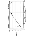
- the film thickness distribution of the thin film when the transparent conductive film was formed on the substrate 1 in the state where the substrate 1 was fixed without moving in the horizontal direction using the thin film deposition apparatus 100 was examined. The result is shown in FIG.
- FIG. 3 is a graph showing the film thickness distribution of the thin film formed on the substrate 1.
- the horizontal axis is the distance (mm) from the right end (exhaust port 10 side) of the substrate 1, and the vertical axis is the film thickness of the thin film.
- a thin film having a thickness of about 1 ⁇ m is uniformly formed in a region (first film formation region) whose distance from the right end of the substrate 1 is 300 to 500 mm.
- first film formation region whose distance from the right end of the substrate 1 is 300 to 500 mm.
- second film formation region the film thickness of the thin film increases as the distance from the first film formation region, that is, the closer to the exhaust port 10 side. It turns out that it becomes thin functionally.
- the thin film deposition method of the present embodiment is a thin film deposition method for depositing a thin film on a substrate, and includes a cooling step for cooling the raw material solution 5 in the sprayer 4 and the mist of the raw material solution 5 by the sprayer 4. 9, and includes a spraying step of spraying the mist 9 onto the substrate 1 from the spraying port of the sprayer 4 and a heating step of heating the mist 9 by the heating unit 3.
- the substrate 1 is disposed below the inside of the heating unit 3. If the vertical distance from the upper surface of the substrate 1 to the upper end of the heating unit 3 is La, the vertical distance Lb from the spray port to the upper surface of the substrate 1 is 1 /. It is characterized by 2La to La.
- the conventional manufacturing methods such as the spray CVD method and the mist CVD method
- the solvent contained in the raw material solution is volatilized and the concentration of the raw material solution may change.
- the conventional film forming method in order to form a thin film with uniform film quality, adjustment such as addition of a solvent to the raw material solution at an appropriate timing is necessary, and the utilization efficiency of the material is low.
- the film formation efficiency is significantly reduced.
- the solvent contained in the raw material solution 5 in the sprayer 4 is less likely to be volatilized.
- the concentration of the solution 5 can be kept uniform. For this reason, it is possible to form a thin film while keeping the concentration of the raw material solution 5 constant, so that the performance of the thin film is stabilized, and the film formation cost is reduced and the productivity is improved. Such merit is considered to increase the effect obtained as the area of the substrate increases.
- the temperature inside the heating unit 3 is preferably maintained at 500 to 600 ° C.
- the cooling step of cooling the raw material solution 5 in the sprayer 4 described above it is preferable to cool the raw material solution 5 in the sprayer 4 to the boiling point of the raw material solution 5 or less. Thereby, volatilization of the solvent contained in the raw material solution 5 can be appropriately controlled.
- the above spraying step may be performed while moving the substrate 1 in a direction substantially perpendicular to the direction in which the mist 9 is sprayed.
- the thin film forming method of this embodiment has a manufacturing advantage in that a thin film having uniform characteristics can be formed.
- a glass substrate is used as the substrate 1, an alkali barrier layer is formed on the glass substrate (first film forming step), and a transparent conductive film is formed on the alkali barrier layer. After that (second film formation step), a semiconductor film and a metal film are formed.
- this glass substrate a soda-lime-silica glass plate that is generally used and inexpensive is generally used.
- This soda lime silica glass plate contains about 10 to 20% by mass of an alkali component such as sodium or potassium, but the alkali component diffuses from the base of the glass substrate to the outside of the glass substrate after long-term use.
- an alkali component such as sodium or potassium
- the transparent conductive film formed on the upper part of the glass substrate becomes cloudy, the transparency decreases, the resistance value of the transparent conductive film increases, or the chemical or physical durability decreases. That is, the redox reaction occurs on the surface of the transparent conductive film due to the alkali diffused from the glass substrate, the material constituting the transparent conductive film is altered, and the thin film solar cell itself undergoes electrolysis, thereby degrading the thin film solar cell.
- an alkali barrier layer may be formed on the surface of the glass substrate.
- the alkali barrier layer and the transparent conductive film are formed by the above-described thin film forming method. Therefore, a high performance thin film solar cell can be manufactured.
- the present invention will be described in more detail with reference to examples, but the present invention is not limited thereto.
- a description will be given of a film forming experiment of a transparent conductive film for a thin film solar cell as an example.
- the present invention is not limited only to the conditions described below, and various thin films such as an alkali barrier layer can be formed by adjusting the heating temperature by the heating unit or by adjusting the material used for the raw material solution. It can be applied to membranes.
- a transparent conductive film was formed on the substrate 1 using the thin film forming apparatus 100 shown in FIG.
- the heating unit 3 is connected to the lower part of the spraying device 6, and the mounting table 2 is installed below the heating unit 3.
- the substrate 1 was fixed on the mounting table 2.
- the atomizer 4 three sprays are used.
- the raw material solution 5 was an aqueous solution containing 0.9 mol / L SnCl 4 and 0.3 M NH 4 F, and containing 30% by mass HCl and 2.5% by mass methanol. The boiling point of this aqueous solution is about 70 ° C.
- the temperature inside the heating unit 3 was set to 590 ° C., and the mist 9 was sprayed for 60 seconds by the sprayer 4 with a water head difference of ⁇ 150 mm to form a transparent conductive film on the 1000 ⁇ 1400 mm substrate.
- the film thickness of the transparent conductive film thus formed was measured with a stylus type surface shape measuring instrument (product name: DEKTAK (manufactured by ULVAC, Inc.)), the results shown in Table 1 were obtained.
- a haze meter Nippon Denshoku Co., Ltd.
- the temperature of the heating part when forming a transparent conductive film was measured with a thermocouple (product name: K thermocouple (manufactured by ASONE Corporation)).
- Example 2 In the configuration of Example 1, a transparent conductive film was formed by changing the vertical distance Lb from the upper surface of the substrate 1 to the upper end of the heating unit 3 from 1/2 La to 2/3 La. Others are the same as in the first embodiment.
- Example 3 In the configuration of Example 1, a transparent conductive film was formed by changing the vertical distance Lb from the upper surface of the substrate 1 to the upper end of the heating unit 3 from 1/2 La to La. Others are the same as in the first embodiment.
- Example 1 In the configuration of Example 1, a transparent conductive film was formed by changing the vertical distance Lb from the upper surface of the substrate 1 to the upper end of the heating unit 3 from 1/2 La to 1/3 La. Others are the same as in the first embodiment.
- ⁇ Comparative example 2> In the configuration of Example 1, a transparent conductive film was formed by changing the vertical distance Lb from the upper surface of the substrate 1 to the upper end of the heating unit 3 from 1/2 La to 4/3 La. Others are the same as in the first embodiment.
- Table 1 shows the measurement results of Examples 1 to 3 and Comparative Examples 1 and 2.
- Example 1 the transparent conductive film formed on the substrate 1 resulted in a larger film thickness as the distance Lb was smaller.
- the film thickness was thin and there was a problem in tact time. Examples 1 to 3 were generally good results.
- the present invention is not limited to the above-described embodiment, and various modifications are possible within the scope shown in the claims, and can be obtained by combining technical means appropriately modified within the scope shown in the claims. Embodiments are also included in the technical scope of the present invention.
- the thickness is 2/3 La to 5/6 La.
- the thin film is preferably a transparent conductive film, and the temperature inside the heating unit is preferably 500 to 600 ° C.
- the temperature inside the heating unit is more preferably 530 to 570 ° C.
- the transparent conductive film can be formed at a high film formation rate.
- the substrate is preferably movable by a moving mechanism.
- the substrate is moved in a direction substantially perpendicular to a direction in which the mist is sprayed.
- the film thickness distribution when the thin film is formed on the substrate with the substrate fixed without moving in the horizontal direction the film thickness is not uniform in the region formed by the mist flowing parallel to the substrate surface.
- the film formation is performed while moving the substrate, a thin film having a uniform film quality can be formed on the entire substrate.
- the cooling means preferably cools the raw material solution in the sprayer to a boiling point or lower of the raw material solution.
- the volatilization of the solvent contained in the raw material solution can be appropriately controlled, and the clogging of the spray port can be prevented.
- the cooling means is a pipe provided around the sprayer, and the raw material solution in the sprayer is water-cooled by the pipe.
- the raw material solution can be easily cooled.
- the embodiment of the present invention can also be expressed as follows.
- a thin film deposition apparatus is a thin film deposition apparatus for depositing a thin film by spraying from a sprayer for spraying the mist onto a substrate by changing the raw material solution into mist, A cooling means for cooling the raw material solution in the sprayer; and a heating part for heating the mist, the heating part being maintained at 500 to 600 ° C., and If the substrate is installed under the interior or the substrate is moved by a moving mechanism, and the vertical distance from the upper surface of the substrate to the upper end of the heating unit is L, from the lower end of the sprayer The vertical distance to the upper surface of the substrate is 1 ⁇ 2 L to L.
- the cooling means preferably cools the raw material solution in the sprayer to a boiling point or lower of the raw material solution.
- the cooling means is a pipe provided around the sprayer, and the raw material solution in the sprayer is water-cooled by the pipe.
- a thin film deposition method is a thin film deposition method for depositing a thin film on a substrate, the step of cooling a raw material solution in a sprayer by air cooling or water cooling, and the sprayer
- the raw material solution is converted into mist by spraying the mist onto the substrate, and the mist is heated by a heating unit maintained at 500 to 600 ° C. from the upper surface of the substrate to the heating unit.
- the vertical distance from the lower end of the sprayer to the upper surface of the substrate is 1 ⁇ 2 L to L, where L is the vertical distance to the upper end of the substrate.
- the step of spraying the mist on the substrate may be performed while moving the substrate in a direction substantially perpendicular to a direction in which the mist is sprayed.
- the present invention is particularly suitable for forming a thin film on a glass substrate used for a thin film solar cell.
Landscapes
- Chemical & Material Sciences (AREA)
- General Chemical & Material Sciences (AREA)
- Chemical Kinetics & Catalysis (AREA)
- Engineering & Computer Science (AREA)
- Materials Engineering (AREA)
- Mechanical Engineering (AREA)
- Metallurgy (AREA)
- Organic Chemistry (AREA)
- Chemical Vapour Deposition (AREA)
- Photovoltaic Devices (AREA)
- Chemically Coating (AREA)
- Manufacturing Of Electric Cables (AREA)
Abstract
本発明に係る薄膜成膜装置(100)は、ミスト(9)を基板(1)に噴霧する噴霧器(4)と、噴霧器(4)内の原料溶液(5)を冷却するための冷却手段と、ミスト(9)を加熱するための加熱部(3)とを有する。基板(1)の上面から加熱部(3)の上端までの鉛直方向の距離をLaとすると、噴霧器(4)の下端から基板(1)の上面までの鉛直方向の距離Lbは、1/2La~Laである。
Description
本発明は、薄膜成膜装置、薄膜成膜方法および薄膜太陽電池の製造方法に関する。
アルカリバリア層や透明導電膜等の薄膜は、半導体、ディスプレイ、太陽電池等の分野で広く利用されている。かかる透明導電膜は、STO(チタン酸ストロンチウム)、ITO(Snドープ酸化インジウム)等の金属酸化物からなるものが用いられており、一般的にはスパッタリング法、蒸着法、有機金属化合物を用いた有機金属化学気相成長法等で成膜される。
しかし、スパッタリング法や蒸着法は、真空プロセスで成膜する必要があるため、真空容器などの真空雰囲気を形成および維持する設備を必要とする。一方、有機金属化学気相成長法は、原料として用いる有機金属化合物が爆発性および毒性を有するため、たとえば排ガス処理装置を設置するなど、薄膜成膜システム全体に高度な安全設計を備える必要がある。以上の理由で、スパッタリング法、蒸着法、および有機金属化学気相成長法はいずれも、低コスト化を図ることが難しい。
そこで、従来とは異なる成膜方法として、ミスト法が提案されている。ミスト法は、原料金属を溶質として含む溶媒を霧化し、これを基板上に噴霧することによって成膜する成膜方法である。
ミスト法は、大気圧で成膜することができるため、真空容器やポンプ類などの製造設備が不要である。しかも、有機金属化合物のような危険物質を用いないため、成膜装置自体の構成が簡便で、かつ低コストで成膜することができる。このようなメリットを有するミスト法は、従来の薄膜成膜方法に代わる新たな方法として期待されている。
このようなミスト法による成膜手段を開示する先行技術文献として、たとえば特許文献1および2を挙げることができる。特許文献1では、まず、金属酸化物を含む原料溶液を超音波振動によって霧化してミストを発生させる。そして、このミストを加熱した上で、基板上に噴射することにより、緻密で均質な膜質の薄膜を成膜する。
また、特許文献2には、噴霧ノズルから噴霧するミストの気化率を高めるために、噴霧ノズルの近傍にキャリアガスを供給するための吹き付けノズルを設けている。そして、ミストの噴霧方向に対し、10~30°程度の角度をつけて斜め方向にキャリアガスを噴き付けている。このようにミストにキャリアガスを噴きつけることにより、ミストが撹乱されて旋回流が生じ、ミストを分散させることができる。
上記の従来技術では、ミストが噴き付けられる基板は、ミスト中に含まれる溶媒を蒸発させるために加熱されるが、この加熱により基板に向かう方向とは逆方向に上昇気流(熱対流)が生じる。この上昇気流によりミストの一部が基板に到達しなくなり、成膜レートが低下するという問題がある。
かかる問題を防止するために、ミストの噴霧圧力を大きくしたり、キャリアガスの流量を多くしたりすることが行なわれている。しかし、噴霧圧力を大きくすると、噴霧ノズルの寿命が短くなるという問題が生じ、キャリアガスの流量を多くすると、ミストの平均粒子径が小さくなる等の理由によって、基板に対しミストを安定して供給することができなくなるという問題が生ずる。また、加熱炉によって噴霧ノズルを熱すると、原料溶液に含まれる溶媒が蒸発し、原料溶液の濃度変化が生じたり、噴霧ノズルの目詰まりが起こったりして、均一に成膜することができなくなる。
本発明は、上記のような現状に鑑みてなされたものであり、その目的とするところは、高い成膜レートで均一な膜質の薄膜を成膜することができる薄膜成膜装置および薄膜成膜方法を提供することにある。
上記の課題を解決するために、本発明に係る薄膜成膜装置は、原料溶液をミストに変えて、該ミストを噴霧口から基板に噴霧する噴霧器を有し、当該噴霧器からの噴霧によって前記基板に薄膜を成膜する薄膜成膜装置であって、前記噴霧器内の前記原料溶液を冷却するための冷却手段と、前記ミストを加熱するための加熱部とを有し、前記基板は、前記加熱部の内部の下方に前記噴霧口に対向して設けられており、前記基板の上面から前記加熱部の上端までの鉛直方向の距離をLaとすると、前記噴霧口から前記基板の上面までの鉛直方向の距離Lbは、1/2La~Laであることを特徴としている。
上記の課題を解決するために、本発明に係る薄膜成膜方法は、基板上に薄膜を成膜するための薄膜成膜方法であって、噴霧器内の原料溶液を冷却する冷却ステップと、前記噴霧器によって前記原料溶液をミストに変え、該ミストを前記噴霧器の噴霧口から前記基板に噴霧する噴霧ステップと、加熱部によって前記ミストを加熱する加熱ステップとを含み、前記基板は、前記加熱部の内部の下方に前記噴霧口に対向して設けられており、前記基板の上面から前記加熱部の上端までの鉛直方向の距離をLaとすると、前記噴霧口から前記基板の上面までの鉛直方向の距離Lbは、1/2La~Laであることを特徴としている。
上記の構成によれば、噴霧器内の原料溶液を冷却するため、噴霧器内の原料溶液に含まれる溶媒が揮発されにくくなり、原料溶液の濃度を均一に保つことができる。このため、原料溶液の濃度を一定に保ちながら、薄膜を成膜することができ、もって薄膜の性質が安定する。また、距離Lbが、1/2La~Laであることにより、ミストを安定して発生させることができ、しかも熱対流が発生することなくミストを基板の上面に到達させることができる。したがって、高い成膜レートで均一な膜質の薄膜を成膜することができる薄膜成膜装置および薄膜成膜方法を提供できる。
本発明に係る薄膜太陽電池の製造方法は、ガラス基板上にアルカリバリア層の薄膜を成膜する第1の成膜ステップを含み、第1の成膜ステップは、上記の薄膜成膜方法の各ステップを含むことを特徴としている。
本発明に係る薄膜太陽電池の製造方法は、ガラス基板上にアルカリバリア層の薄膜を成膜する第1の成膜ステップと、前記アルカリバリア層上に透明導電膜の薄膜を成膜する第2の成膜ステップとを含み、第1の成膜ステップおよび第2の成膜ステップの少なくともいずれかのステップは、上記の薄膜成膜方法の各ステップを含むことを特徴としている。
上記の構成によれば、透明導電膜および/またはアルカリバリア層をガラス基板上に均一に成膜することができるので、高性能の薄膜太陽電池を製造することができる。
以上のように、本発明に係る薄膜成膜装置は、原料溶液をミストに変えて、該ミストを噴霧口から基板に噴霧する噴霧器を有し、当該噴霧器からの噴霧によって前記基板に薄膜を成膜する薄膜成膜装置であって、前記噴霧器内の前記原料溶液を冷却するための冷却手段と、前記ミストを加熱するための加熱部とを有し、前記基板は、前記加熱部の内部の下方に前記噴霧口に対向して設けられており、前記基板の上面から前記加熱部の上端までの鉛直方向の距離をLaとすると、前記噴霧口から前記基板の上面までの鉛直方向の距離Lbは、1/2La~Laである。また、本発明に係る薄膜成膜方法は、基板上に薄膜を成膜するための薄膜成膜方法であって、噴霧器内の原料溶液を冷却する冷却ステップと、前記噴霧器によって前記原料溶液をミストに変え、該ミストを前記噴霧器の噴霧口から前記基板に噴霧する噴霧ステップと、加熱部によって前記ミストを加熱する加熱ステップとを含み、前記基板は、前記加熱部の内部の下方に前記噴霧口に対向して設けられており、前記基板の上面から前記加熱部の上端までの鉛直方向の距離をLaとすると、前記噴霧口から前記基板の上面までの鉛直方向の距離Lbは、1/2La~Laである。したがって、高い成膜レートで均一な膜質の薄膜を成膜することができる薄膜成膜装置および薄膜成膜方法を提供できるという効果を奏する。
以下、本発明の実施形態について図面を用いて説明する。図面において、同一の参照符号は、同一部分または相当部分を表わすものである。また、長さ、幅、厚さ、深さなどの寸法関係は図面の明瞭化と簡略化のために適宜に変更されており、実際の寸法関係を表わすものではない。
〔薄膜成膜装置の構成〕
図1は、本発明の薄膜成膜装置の一例である薄膜成膜装置100を模式的に示す断面図である。薄膜成膜装置100は、基板1上に薄膜(図示せず)を成膜するためのものであって、加熱部3と噴霧装置6とを備えている。
図1は、本発明の薄膜成膜装置の一例である薄膜成膜装置100を模式的に示す断面図である。薄膜成膜装置100は、基板1上に薄膜(図示せず)を成膜するためのものであって、加熱部3と噴霧装置6とを備えている。
<加熱部3>
加熱部3は、直方体の容器であり、その内部が高温に保持されている。加熱部3内部の下方に載積台2が設けられている。載積台2上には基板1が載積されており、該基板1は成膜中に加熱部3によって加熱される。載積台2は、移動機構(図示せず)を有しており、基板1の成膜面方向に1軸移動しながら、基板上に薄膜を成膜する。すなわち、加熱部3の内部には、基板1を含む載積台2および移動機構が収容される。なお、成膜中に載積台2は必ずしも成膜面方向に1軸移動する必要はなく、成膜中に載積台2が停止しても差し支えない。
加熱部3は、直方体の容器であり、その内部が高温に保持されている。加熱部3内部の下方に載積台2が設けられている。載積台2上には基板1が載積されており、該基板1は成膜中に加熱部3によって加熱される。載積台2は、移動機構(図示せず)を有しており、基板1の成膜面方向に1軸移動しながら、基板上に薄膜を成膜する。すなわち、加熱部3の内部には、基板1を含む載積台2および移動機構が収容される。なお、成膜中に載積台2は必ずしも成膜面方向に1軸移動する必要はなく、成膜中に載積台2が停止しても差し支えない。
加熱部3の上面には穴が開けられており、該穴に噴霧装置6が嵌められている。これにより、噴霧装置6の下部は加熱部3に覆われている。
<噴霧装置6>
噴霧装置6は、ガス導入口7および排気口10を有する筐体と、該筐体の内部に取り付けられた噴霧器4とを備えている。
噴霧装置6は、ガス導入口7および排気口10を有する筐体と、該筐体の内部に取り付けられた噴霧器4とを備えている。
<噴霧器4>
噴霧器4は、原料溶液5をミスト9に変えて、該ミスト9をノズル8から基板1に噴霧するものであり、超音波霧化またはスプレー噴霧によってミスト9を発生させることができる。ここで、超音波霧化を用いてミストを発生させる場合、超音波振動子によってミストを発生させることが好ましい。超音波振動子は、比較的均一な平均粒子径のミストを噴霧することができるため、ミスト同士がより凝集しにくくなるという利点がある。
噴霧器4は、原料溶液5をミスト9に変えて、該ミスト9をノズル8から基板1に噴霧するものであり、超音波霧化またはスプレー噴霧によってミスト9を発生させることができる。ここで、超音波霧化を用いてミストを発生させる場合、超音波振動子によってミストを発生させることが好ましい。超音波振動子は、比較的均一な平均粒子径のミストを噴霧することができるため、ミスト同士がより凝集しにくくなるという利点がある。
ノズル8は、噴霧器4の先端に取り付けられており、例えば、2流体スプレーノズルで構成される。この場合、ノズル8において、圧縮空気と原料溶液とが混ざり合うことによりミスト9となる。噴霧器4の個数は、タクトタイムに必要とされる単位時間当たりの噴霧量によって変更してもよいし、成膜に必要な成膜レートに応じて変更してもよい。
ここで、「ミスト」とは、平均粒子径が0.1μm以上100μm以下の液滴が気体に分散された状態のものをいう。かかるミストの平均粒子径は、液浸法によって算出された値を採用するものとする。
また、噴霧器4内には、図示しない冷却手段が設けられている。
<冷却手段>
本実施形態において、冷却手段は、噴霧器4内の原料溶液5を冷却するために設けられるものである。このような冷却手段によって噴霧器4内の原料溶液5を冷却することにより、噴霧器4の先端のノズル詰まりを防止することができる。
本実施形態において、冷却手段は、噴霧器4内の原料溶液5を冷却するために設けられるものである。このような冷却手段によって噴霧器4内の原料溶液5を冷却することにより、噴霧器4の先端のノズル詰まりを防止することができる。
ノズル詰まりを防止するという観点からは、噴霧器4内の原料溶液5を、該原料溶液5の沸点以下の温度に冷却することが好ましい。原料溶液5をこのような温度に冷却することにより、原料溶液5中の溶媒が揮発しにくくなる。よって、原料溶液5の濃度を一定に保つことができるとともに、噴霧器4の先端のノズル詰まりを防止することができる。
上記の冷却手段は、噴霧器4内の原料溶液5を室温程度に冷却するものであることがより好ましい。
なお、冷却手段は、空冷によって原料溶液を冷却してもよいし、水冷によって原料溶液を冷却してもよく、両者を併用しても差し支えない。空冷による冷却方法としては、ファンを挙げることができ、水冷による冷却手段としては、噴霧器の周辺に設けられた配管を挙げることができる。
このように噴霧器4内の原料溶液5を冷却手段によって冷却することにより、原料溶液5に含まれる溶媒が蒸発しにくくなり、もって噴霧器4のノズル詰まりや、噴霧器4の変形を防止することができる。
<原料溶液5>
原料溶液5としては、亜鉛、スズ、インジウム、カドミウム、およびストロンチウムからなる群より選択される無機材料の塩化物または有機金属化合物を溶媒に溶解させたものを用いることが好ましい。原料溶液5に用いる溶媒としては、水、メタノール、エタノール、ブタノール等を挙げることができる。このような原料溶液5としては、酢酸亜鉛を含む水溶液、酸化インジウム錫を含む水溶液、酸化錫を含む水溶液等を挙げることができる。上記の原料溶液5の濃度は、特に限定されないが、一般的には0.1~3mol/Lの濃度の塩化物または有機金属化合物を含むものを用いることが好ましい。
原料溶液5としては、亜鉛、スズ、インジウム、カドミウム、およびストロンチウムからなる群より選択される無機材料の塩化物または有機金属化合物を溶媒に溶解させたものを用いることが好ましい。原料溶液5に用いる溶媒としては、水、メタノール、エタノール、ブタノール等を挙げることができる。このような原料溶液5としては、酢酸亜鉛を含む水溶液、酸化インジウム錫を含む水溶液、酸化錫を含む水溶液等を挙げることができる。上記の原料溶液5の濃度は、特に限定されないが、一般的には0.1~3mol/Lの濃度の塩化物または有機金属化合物を含むものを用いることが好ましい。
<基板1と噴霧器4との位置関係>
本実施形態では、基板1の上面から加熱部3の上端までの鉛直方向の距離をLaとすると、噴霧器4の下端(噴霧口)から基板1の上面までの鉛直方向の距離Lbは、1/2La~Laとなっている。これにより、噴霧圧力および排気流量を適切に設定することにより、ミスト9を安定して発生させることができ、しかも熱対流が発生することなくミスト9を基板1の上面に到達させることができる。さらに好ましくは、噴霧器4の下端から基板1の上面までの鉛直方向の距離Lbは、2/3La~5/6Laである。
本実施形態では、基板1の上面から加熱部3の上端までの鉛直方向の距離をLaとすると、噴霧器4の下端(噴霧口)から基板1の上面までの鉛直方向の距離Lbは、1/2La~Laとなっている。これにより、噴霧圧力および排気流量を適切に設定することにより、ミスト9を安定して発生させることができ、しかも熱対流が発生することなくミスト9を基板1の上面に到達させることができる。さらに好ましくは、噴霧器4の下端から基板1の上面までの鉛直方向の距離Lbは、2/3La~5/6Laである。
なお、距離Lbが1/2La未満であると、噴霧される原料溶液5の加熱が不十分であるため、原料溶液5に含まれる溶媒を気化させるのに時間を要することになり好ましくない。一方、距離LbがLaを超えると、ミスト9が噴霧されるノズル8の噴霧口から基板1までの間における、温度の高い領域が占める割合が大きくなるため、ミスト9に含まれる溶媒成分が気化して、ミスト9の重力や慣性力が弱まる。これにより、ミスト9が基板1に到達しにくくなり、薄膜の成膜レートが低下する傾向がある。
<加熱部3内の温度>
また、加熱部3内の温度は、成膜する薄膜によって適切な温度が異なるため一律に最適な温度を規定することは困難であるが、たとえば透明導電膜を成膜する場合は、加熱部3内の温度を500~600℃として成膜することが好ましく、530~570℃で成膜することがさらに好ましい。
また、加熱部3内の温度は、成膜する薄膜によって適切な温度が異なるため一律に最適な温度を規定することは困難であるが、たとえば透明導電膜を成膜する場合は、加熱部3内の温度を500~600℃として成膜することが好ましく、530~570℃で成膜することがさらに好ましい。
なお、加熱部3内の温度が500℃未満であると、ミスト9に含まれる溶媒が揮発しにくくなるため、透明導電膜の成膜レートが著しく低下することになる。一方、加熱部3内の温度が600℃を超えると、ミスト9が基板1に到達する前にミスト9中の溶媒が揮発し、ミスト9が基板1の表面に到達しにくくなる。
ここで、上記の「透明導電膜」は、透明性および導電性を要求されるものであり、たとえばITO、STO等からなるものである。これに対し、「アルカリバリア層」は、基板に含まれるアルカリ成分が基板外に放出されることを防止するために設けられるものである。アルカリバリア層は、基板1がアルカリ成分を含まない場合またはアルカリ成分を微量程度に含む場合は必ずしも基板1の表面に設けなくてもよく、このようなアルカリバリア層はSiO2からなるものであることが好ましい。
<構成のまとめ>
以上のように、薄膜成膜装置100は、図1に示されるように、原料溶液5をミスト9に変えて、該ミスト9を噴霧口から基板1に噴霧する噴霧器4を有し、噴霧器4からの噴霧によって基板1に薄膜(図示せず)を成膜する薄膜成膜装置であって、噴霧器4内の原料溶液5を冷却するための冷却手段と、加熱部3とを有し、基板1は、加熱部3の内部の下方に前記噴霧口に対向して設けられており、基板1の上面から加熱部3の上端までの鉛直方向の距離をLaとすると、前記噴霧口から基板1の上面までの鉛直方向の距離Lbは、1/2La~Laであることを特徴としている。
以上のように、薄膜成膜装置100は、図1に示されるように、原料溶液5をミスト9に変えて、該ミスト9を噴霧口から基板1に噴霧する噴霧器4を有し、噴霧器4からの噴霧によって基板1に薄膜(図示せず)を成膜する薄膜成膜装置であって、噴霧器4内の原料溶液5を冷却するための冷却手段と、加熱部3とを有し、基板1は、加熱部3の内部の下方に前記噴霧口に対向して設けられており、基板1の上面から加熱部3の上端までの鉛直方向の距離をLaとすると、前記噴霧口から基板1の上面までの鉛直方向の距離Lbは、1/2La~Laであることを特徴としている。
上記の構成によれば、噴霧器4内の原料溶液5を冷却するため、噴霧器4内の原料溶液5に含まれる溶媒が揮発されにくくなり、原料溶液5の濃度を均一に保つことができる。このため、原料溶液5の濃度を一定に保ちながら、薄膜を成膜することができ、もって薄膜の性質が安定する。また、距離Lbが、1/2La~Laであることにより、ミスト9を安定して発生させることができ、しかも熱対流が発生することなくミスト9を基板1の上面に到達させることができる。したがって、高い成膜レートで均一な膜質の薄膜を成膜することができる。
〔薄膜成膜装置100の動作〕
続いて、薄膜成膜装置100の動作を説明する。
続いて、薄膜成膜装置100の動作を説明する。
薄膜成膜装置100では、まず、ガス導入口7から噴霧器4に圧縮空気を導入すると、噴霧器4が薄膜材料溶液タンクから原料溶液5を吸上げ、原料溶液5をミスト9に変えて、噴霧器4先端のノズル8からミスト9を噴出する。前記圧縮空気は、たとえば窒素、酸素、水素、およびこれらの混合ガスを用いることができる。
基板1の上面においては、噴霧器4による垂直方向に流れるミスト9の成膜に加え、基板1が移動する方向に平行な水平方向に流れるミスト9によっても水平方向の成膜がなされる。成膜されなかった余分な噴霧ミストは、排気口10および図示しない除害装置を経て、排気口出口から外部に放出される。このように、薄膜成膜装置100では、キャリアガスを用いず、図1の矢印で示すように、ガス導入口7と排気口10とがほとんど直接つながっている。なお、噴霧器4に導入される圧縮空気の量、および噴霧器4から排気される排気量は、適宜設定することができる。
〔成膜ライン200〕
図2は、本実施形態の薄膜成膜装置100を組み込んだ成膜ライン200を模式的に示す断面図である。成膜ライン200では、基板1が、ベルトコンベア(移動機構)によって図中右方向に例えば10mm/secで搬送され、加熱部17に投入されて静止する。該加熱部17で加熱された基板1は、その後、薄膜成膜装置100の成膜部(図1の下方)導入される。この成膜部で、基板1上にアルカリバリア層または透明導電膜のような薄膜が成膜される。この成膜は、ミスト9を噴霧する方向と略垂直方向に基板1を移動させながら行ってもよい。その後、基板1は除冷部18に導入されて静止する。除冷部18において、基板1および薄膜が除冷されると、薄膜が形成された基板1が完成する。薄膜が形成された基板1は、図2の右端の取り出し口から取り出される。
図2は、本実施形態の薄膜成膜装置100を組み込んだ成膜ライン200を模式的に示す断面図である。成膜ライン200では、基板1が、ベルトコンベア(移動機構)によって図中右方向に例えば10mm/secで搬送され、加熱部17に投入されて静止する。該加熱部17で加熱された基板1は、その後、薄膜成膜装置100の成膜部(図1の下方)導入される。この成膜部で、基板1上にアルカリバリア層または透明導電膜のような薄膜が成膜される。この成膜は、ミスト9を噴霧する方向と略垂直方向に基板1を移動させながら行ってもよい。その後、基板1は除冷部18に導入されて静止する。除冷部18において、基板1および薄膜が除冷されると、薄膜が形成された基板1が完成する。薄膜が形成された基板1は、図2の右端の取り出し口から取り出される。
〔膜厚分布〕
薄膜成膜装置100においては、図1に示されるように、基板1に垂直な方向のミスト9によって薄膜が成膜される領域(第1成膜領域)と、基板1が移動する方向に平行な水平方向に流れるミスト9によって成膜される領域(第2成膜領域)とがある。ここで、薄膜成膜装置100を用いて、基板1を水平方向に移動させずに固定した状態で、基板1上に透明導電膜を成膜したときの薄膜の膜厚分布を調べた。その結果を図2に示す。
薄膜成膜装置100においては、図1に示されるように、基板1に垂直な方向のミスト9によって薄膜が成膜される領域(第1成膜領域)と、基板1が移動する方向に平行な水平方向に流れるミスト9によって成膜される領域(第2成膜領域)とがある。ここで、薄膜成膜装置100を用いて、基板1を水平方向に移動させずに固定した状態で、基板1上に透明導電膜を成膜したときの薄膜の膜厚分布を調べた。その結果を図2に示す。
図3は、基板1上に形成された薄膜の膜厚分布を示すグラフである。横軸は、基板1の右端(排気口10側)からの距離(mm)であり、縦軸は、薄膜の膜厚である。
図3に示されるように、基板1の右端からの距離が300~500mmの領域(第1成膜領域)では、1μm程度の厚みの薄膜が均一に成膜されている。これに対し、基板1の右端からの距離が100~300mmの領域(第2成膜領域)では、第1成膜領域から離れるほど、すなわち排気口10側に近づくほど薄膜の膜厚が1次関数的に薄くなることがわかる。
〔薄膜成膜方法〕
本実施形態の薄膜成膜方法は、基板上に薄膜を成膜するための薄膜成膜方法であって、噴霧器4内の原料溶液5を冷却する冷却ステップと、噴霧器4によって原料溶液5をミスト9に変え、該ミスト9を噴霧器4の噴霧口から基板1に噴霧する噴霧ステップと、加熱部3によってミスト9を加熱する加熱ステップとを含み、基板1は、加熱部3の内部の下方に噴霧口に対向して設けられており、基板1の上面から加熱部3の上端までの鉛直方向の距離をLaとすると、噴霧口から基板1の上面までの鉛直方向の距離Lbは、1/2La~Laであることを特徴としている。
本実施形態の薄膜成膜方法は、基板上に薄膜を成膜するための薄膜成膜方法であって、噴霧器4内の原料溶液5を冷却する冷却ステップと、噴霧器4によって原料溶液5をミスト9に変え、該ミスト9を噴霧器4の噴霧口から基板1に噴霧する噴霧ステップと、加熱部3によってミスト9を加熱する加熱ステップとを含み、基板1は、加熱部3の内部の下方に噴霧口に対向して設けられており、基板1の上面から加熱部3の上端までの鉛直方向の距離をLaとすると、噴霧口から基板1の上面までの鉛直方向の距離Lbは、1/2La~Laであることを特徴としている。
従来のスプレーCVD法やミストCVD法等の製造方法では、噴霧器内の原料溶液が加熱されることにより、原料溶液に含まれる溶媒の揮発が生じ、原料溶液の濃度が変わることがあった。このため、従来の成膜方法では、均一な膜質の薄膜を成膜するために、原料溶液に溶媒を適切なタイミングで添加する等の調整が必要であり、材料の利用効率が低かった。特に、ミストを噴霧して薄膜を成膜するミストCVD装置で成膜する場合に、成膜効率の低下が顕著であった。
これに対し、本実施形態の薄膜成膜方法では、空冷式または水冷式によって噴霧器4内の原料溶液5を冷却するため、噴霧器4内の原料溶液5に含まれる溶媒が揮発されにくくなり、原料溶液5の濃度を均一に保つことができる。このため、原料溶液5の濃度を一定に保ちながら、薄膜を成膜することができ、もって薄膜の性能が安定するとともに、成膜コストの低減や生産性の向上にも寄与することになる。このようなメリットは、基板の面積が大きいほど得られる効果が大きくなるものと考えられる。
上記の薄膜成膜方法を用いて透明導電膜を成膜する場合は、加熱部3の内部の温度は、500~600℃に保持することが好ましい。
上記の噴霧器4内の原料溶液5を冷却する冷却ステップでは、噴霧器4内の原料溶液5を、原料溶液5の沸点以下に冷却することが好ましい。これにより原料溶液5に含まれる溶媒の揮発を適切に制御することができる。
また、上記の噴霧ステップは、ミスト9を噴霧する方向と略垂直方向に基板1を移動させながら行なってもよい。このように基板1を移動させながら薄膜を成膜しても、均一な特性を有する薄膜を形成することができるという点で、本実施形態の薄膜成膜方法は製造上のメリットがある。
<薄膜太陽電池への適用>
薄膜太陽電池を製造する場合、基板1としてガラス基板を用い、該ガラス基板上にアルカリバリア層を成膜し(第1の成膜ステップ)、さらに、アルカリバリア層上に透明導電膜を成膜した上で(第2の成膜ステップ)、半導体膜および金属膜を形成することによって作製する。このガラス基板としては、汎用的に使用され価格的にも安価なソーダライムシリカガラス板を用いるのが一般的である。
薄膜太陽電池を製造する場合、基板1としてガラス基板を用い、該ガラス基板上にアルカリバリア層を成膜し(第1の成膜ステップ)、さらに、アルカリバリア層上に透明導電膜を成膜した上で(第2の成膜ステップ)、半導体膜および金属膜を形成することによって作製する。このガラス基板としては、汎用的に使用され価格的にも安価なソーダライムシリカガラス板を用いるのが一般的である。
このソーダライムシリカガラス板は、ナトリウム、カリウム等のアルカリ成分を10~20質量%程度含むものであるが、長期間の使用によりガラス基板の下地からアルカリ成分がガラス基板の外部に拡散する。これによりガラス基板の上部に形成された透明導電膜が白濁したり、透明度が低下したり、透明導電膜の抵抗値が増大したり、化学的または物理的な耐久性が低下したりする。すなわち、ガラス基板から拡散したアルカリにより透明導電膜の表面で酸化還元反応が起こり、透明導電膜を構成する材料が変質し、さらに薄膜太陽電池自体が電気分解を起こすことにより、薄膜太陽電池が劣化する。このような不具合を防止するために、ガラス基板の表面にアルカリバリア層を形成することがある。
本実施形態では、上記の薄膜成膜方法によってアルカリバリア層および透明導電膜の成膜を行なう。したがって、高性能の薄膜太陽電池を製造することができる。
以下、実施例を挙げて本発明をより詳細に説明するが、本発明はこれらに限定されるものではない。本実施例では、薄膜太陽電池向けの透明導電膜の成膜実験を例にとり説明する。なお、本発明は以下に説明する条件のみに限られるものではなく、加熱部による加熱温度を調整するか、または原料溶液に用いる材料を調整することにより、アルカリバリア層などのさまざまな薄膜の成膜に応用することができる。
<実施例1>
本実施例では、図1に示される薄膜成膜装置100を用いて基板1上に透明導電膜を成膜した。図1の薄膜成膜装置100は、噴霧装置6の下部に加熱部3が接続されており、加熱部3の内部の下方には載積台2が設置されている。この載積台2上に基板1を固定した。噴霧器4としては、3個のスプレーを用いている。
本実施例では、図1に示される薄膜成膜装置100を用いて基板1上に透明導電膜を成膜した。図1の薄膜成膜装置100は、噴霧装置6の下部に加熱部3が接続されており、加熱部3の内部の下方には載積台2が設置されている。この載積台2上に基板1を固定した。噴霧器4としては、3個のスプレーを用いている。
基板1の上面から加熱部3の上端までの鉛直方向の距離をLaとすると、この噴霧器4の下端から基板1の上面までの鉛直方向の距離Lbは1/2Laである。また、原料溶液5としては、0.9mol/LのSnCl4と、0.3MのNH4Fとを含み、30質量%のHClと2.5質量%のメタノールとを含む水溶液を用いた。この水溶液の沸点は約70℃程度である。
そして、上記の加熱部3の内部の温度を590℃として、-150mmの水頭差で噴霧器4によってミスト9を60秒間噴霧することにより、1000×1400mmの基板上に透明導電膜を成膜した。このようにして成膜した透明導電膜の膜厚を触針式表面形状測定器(製品名:DEKTAK(株式会社アルバック製))によって測定したところ、表1のような結果となった。
なお、ヘイズ率とは、ヘイズ(%)={全光線透過率(%)-平行光線透過率(%)}/全光線透過率(%)で示される数値を使用し、ヘイズメーター(NDH4000;日本電色株式会社)によって測定を行った。また、透明導電膜を成膜するときの加熱部の温度は、熱電対(製品名:K熱電対(アズワン株式会社製))によって測定した。
<実施例2>
実施例1の構成において、基板1の上面から加熱部3の上端までの鉛直方向の距離Lbを1/2Laから2/3Laに代えて、透明導電膜を成膜した。その他は、実施例1と同様である。
実施例1の構成において、基板1の上面から加熱部3の上端までの鉛直方向の距離Lbを1/2Laから2/3Laに代えて、透明導電膜を成膜した。その他は、実施例1と同様である。
<実施例3>
実施例1の構成において、基板1の上面から加熱部3の上端までの鉛直方向の距離Lbを1/2LaからLaに代えて、透明導電膜を成膜した。その他は、実施例1と同様である。
実施例1の構成において、基板1の上面から加熱部3の上端までの鉛直方向の距離Lbを1/2LaからLaに代えて、透明導電膜を成膜した。その他は、実施例1と同様である。
<比較例1>
実施例1の構成において、基板1の上面から加熱部3の上端までの鉛直方向の距離Lbを1/2Laから1/3Laに代えて、透明導電膜を成膜した。その他は、実施例1と同様である。
実施例1の構成において、基板1の上面から加熱部3の上端までの鉛直方向の距離Lbを1/2Laから1/3Laに代えて、透明導電膜を成膜した。その他は、実施例1と同様である。
<比較例2>
実施例1の構成において、基板1の上面から加熱部3の上端までの鉛直方向の距離Lbを1/2Laから4/3Laに代えて、透明導電膜を成膜した。その他は、実施例1と同様である。
実施例1の構成において、基板1の上面から加熱部3の上端までの鉛直方向の距離Lbを1/2Laから4/3Laに代えて、透明導電膜を成膜した。その他は、実施例1と同様である。
<測定結果>
実施例1~3および比較例1~2の測定結果を表1に示す。
実施例1~3および比較例1~2の測定結果を表1に示す。

実施例1~3では、基板1上に成膜された透明導電膜は、距離Lbが小さいほど膜厚が大きくなる結果となった。基板1に近い距離で噴霧した場合の膜厚、すなわち比較例1で示した膜厚はもっとも大きかったが、抵抗値が大きく、膜ムラが非常に大きい結果となった。比較例2の結果では、膜厚が薄く、タクトタイムに問題があった。実施例1~3は、おおむね良好な結果であった。
(付記事項)
以上のように本発明の実施形態および実施例について説明を行なったが、上述の実施の形態および実施例の構成を適宜組み合わせることも当初から予定している。
以上のように本発明の実施形態および実施例について説明を行なったが、上述の実施の形態および実施例の構成を適宜組み合わせることも当初から予定している。
今回開示された実施形態および実施例はすべての点で例示であって制限的なものではないと考えられるべきである。本発明の範囲は、上記した説明ではなく特許請求の範囲によって示され、特許請求の範囲と均等の意味および範囲内でのすべての変更が含まれることが意図される。
すなわち、本発明は上述した実施形態に限定されるものではなく、請求項に示した範囲で種々の変更が可能であり、請求項に示した範囲で適宜変更した技術的手段を組み合わせて得られる実施形態についても本発明の技術的範囲に含まれる。
本発明の実施形態に係る薄膜成膜装置では、2/3La~5/6Laであることがさらに好ましい。
本発明の実施形態に係る薄膜成膜装置および薄膜成膜方法では、前記薄膜は透明導電膜であり、前記加熱部の内部の温度は、500~600℃であることが好ましい。
本発明の実施形態に係る薄膜成膜装置では、前記加熱部の内部の温度は、530~570℃であることがさらに好ましい。
上記の構成によれば、高い成膜レートで透明導電膜を成膜することができる。
本発明の実施形態に係る薄膜成膜装置では、前記基板は、移動機構によって移動可能であることが好ましい。
本発明の実施形態に係る薄膜成膜方法では、前記噴霧ステップでは、前記ミストを噴霧する方向と略垂直方向に前記基板を移動させることが好ましい。
基板を水平方向に移動させずに固定した状態で、基板上に薄膜を成膜したときの膜厚分布では、基板面に平行に流れるミストによって成膜される領域では、膜厚が均一にならない。これに対し、上記の構成によれば、基板を移動させながら成膜を行なうので、基板全体に均一な膜質の薄膜を成膜することができる。
本発明の実施形態に係る薄膜成膜装置では、前記冷却手段は、前記噴霧器内の前記原料溶液を、該原料溶液の沸点以下に冷却することが好ましい。
上記の構成によれば、原料溶液に含まれる溶媒の揮発を適切に制御することができ、噴霧口の詰まりを防止することができる。
本発明の実施形態に係る薄膜成膜装置では、前記冷却手段は、前記噴霧器の周辺に設けられた配管であり、前記配管によって前記噴霧器内の前記原料溶液が水冷されることが好ましい。
上記の構成によれば、容易に原料溶液を冷却することができる。
なお、本発明の実施形態は以下のようにも表現することができる。
本発明の実施形態に係る薄膜成膜装置は、原料溶液をミストに変えて、該ミストを基板に噴霧するための噴霧器からの噴霧によって薄膜を成膜するための薄膜成膜装置であって、前記噴霧器内の前記原料溶液を冷却するための冷却手段と、前記ミストを加熱するための加熱部とを有し、前記加熱部は、その内部が500~600℃に保持されており、かつその内部の下方に前記基板が設置されているか、または前記基板が移動機構によって移動されており、前記前記基板の上面から前記加熱部の上端までの鉛直方向の距離をLとすると、噴霧器の下端から前記基板の上面までの鉛直方向の距離は、1/2L~Lであることを特徴としている。
本発明の実施形態に係る薄膜成膜装置では、前記冷却手段は、前記噴霧器内の前記原料溶液を、該原料溶液の沸点以下に冷却することが好ましい。
本発明の実施形態に係る薄膜成膜装置では、前記冷却手段は、前記噴霧器の周辺に設けられた配管であり、前記配管によって前記噴霧器内の前記原料溶液が水冷されることが好ましい。
本発明の実施形態に係る薄膜成膜方法は、基板上に薄膜を成膜するための薄膜成膜方法であって、空冷式または水冷式によって噴霧器内の原料溶液を冷却するステップと、前記噴霧器によって前記原料溶液をミストに変え、該ミストを前記基板に噴霧するステップと、500~600℃に保持された加熱部によって前記ミストを加熱するステップとを含み、前記前記基板の上面から前記加熱部の上端までの鉛直方向の距離をLとすると、噴霧器の下端から前記基板の上面までの鉛直方向の距離は、1/2L~Lであることを特徴としている。
本発明の実施形態に係る薄膜成膜方法では、前記ミストを前記基板に噴霧するステップは、前記ミストを噴き付ける方向と略垂直方向に前記基板を移動させながら行なってもよい。
本発明は、特に、薄膜太陽電池に用いられるガラス基板への薄膜成膜に好適である。
1 基板
2 載積台
3 加熱部
4 噴霧器
5 原料溶液
6 噴霧装置
7 ガス導入口
8 ノズル
9 ミスト
10 排気口
17 加熱部
18 除冷部
100 薄膜成膜装置
200 成膜ライン
2 載積台
3 加熱部
4 噴霧器
5 原料溶液
6 噴霧装置
7 ガス導入口
8 ノズル
9 ミスト
10 排気口
17 加熱部
18 除冷部
100 薄膜成膜装置
200 成膜ライン
Claims (13)
- 原料溶液をミストに変えて、該ミストを噴霧口から基板に噴霧する噴霧器を有し、
当該噴霧器からの噴霧によって前記基板に薄膜を成膜する薄膜成膜装置であって、
前記噴霧器内の前記原料溶液を冷却するための冷却手段と、
前記ミストを加熱するための加熱部とを有し、
前記基板は、前記加熱部の内部の下方に前記噴霧口に対向して設けられており、
前記基板の上面から前記加熱部の上端までの鉛直方向の距離をLaとすると、前記噴霧口から前記基板の上面までの鉛直方向の距離Lbは、1/2La~Laであることを特徴とする薄膜成膜装置。 - 前記距離Lbは、2/3La~5/6Laであることを特徴とする請求項1に記載の薄膜成膜装置。
- 前記薄膜は透明導電膜であり、
前記加熱部の内部の温度は、500~600℃であることを特徴とする請求項1または2に記載の薄膜成膜装置。 - 前記加熱部の内部の温度は、530~570℃であることを特徴とする請求項3に記載の薄膜成膜装置。
- 前記基板は、移動機構によって移動可能であることを特徴とする請求項1~4のいずれか1項に記載の薄膜成膜装置。
- 前記冷却手段は、前記噴霧器内の前記原料溶液を、該原料溶液の沸点以下に冷却することを特徴とする請求項1~5のいずれか1項に記載の薄膜成膜装置。
- 前記冷却手段は、前記噴霧器の周辺に設けられた配管であり、
前記配管によって前記噴霧器内の前記原料溶液が水冷されることを特徴とする請求項1~6のいずれか1項に記載の薄膜成膜装置。 - 基板上に薄膜を成膜するための薄膜成膜方法であって、
噴霧器内の原料溶液を冷却する冷却ステップと、
前記噴霧器によって前記原料溶液をミストに変え、該ミストを前記噴霧器の噴霧口から前記基板に噴霧する噴霧ステップと、
加熱部によって前記ミストを加熱する加熱ステップとを含み、
前記基板は、前記加熱部の内部の下方に前記噴霧口に対向して設けられており、
前記基板の上面から前記加熱部の上端までの鉛直方向の距離をLaとすると、前記噴霧口から前記基板の上面までの鉛直方向の距離Lbは、1/2La~Laであることを特徴とする薄膜成膜方法。 - 前記薄膜は透明導電膜であり、
前記加熱部の内部の温度は、500~600℃であることを特徴とする請求項8に記載の薄膜成膜方法。 - 前記噴霧ステップでは、前記ミストを噴霧する方向と略垂直方向に前記基板を移動させることを特徴とする請求項8または9に記載の薄膜成膜方法。
- 前記冷却ステップでは、前記噴霧器内の前記原料溶液を、該原料溶液の沸点以下に冷却することを特徴とする請求項8~10のいずれか1項に記載の薄膜成膜方法。
- ガラス基板上にアルカリバリア層の薄膜を成膜する第1の成膜ステップを含む薄膜太陽電池の製造方法であって、
第1の成膜ステップは、請求項8~11のいずれか1項に記載の薄膜成膜方法の各ステップを含むことを特徴とする薄膜太陽電池の製造方法。 - ガラス基板上にアルカリバリア層の薄膜を成膜する第1の成膜ステップと、
前記アルカリバリア層上に透明導電膜の薄膜を成膜する第2の成膜ステップとを含む薄膜太陽電池の製造方法であって、
第1の成膜ステップおよび第2の成膜ステップの少なくともいずれかのステップは、請求項8~11のいずれか1項に記載の薄膜成膜方法の各ステップを含むことを特徴とする薄膜太陽電池の製造方法。
Applications Claiming Priority (2)
| Application Number | Priority Date | Filing Date | Title |
|---|---|---|---|
| JP2011-279049 | 2011-12-20 | ||
| JP2011279049A JP5148743B1 (ja) | 2011-12-20 | 2011-12-20 | 薄膜成膜装置、薄膜成膜方法および薄膜太陽電池の製造方法 |
Publications (1)
| Publication Number | Publication Date |
|---|---|
| WO2013094232A1 true WO2013094232A1 (ja) | 2013-06-27 |
Family
ID=47890558
Family Applications (1)
| Application Number | Title | Priority Date | Filing Date |
|---|---|---|---|
| PCT/JP2012/058797 Ceased WO2013094232A1 (ja) | 2011-12-20 | 2012-04-02 | 薄膜成膜装置、薄膜成膜方法および薄膜太陽電池の製造方法 |
Country Status (2)
| Country | Link |
|---|---|
| JP (1) | JP5148743B1 (ja) |
| WO (1) | WO2013094232A1 (ja) |
Cited By (1)
| Publication number | Priority date | Publication date | Assignee | Title |
|---|---|---|---|---|
| TWI603418B (zh) * | 2016-04-26 | 2017-10-21 | 東芝三菱電機產業系統股份有限公司 | 成膜裝置 |
Families Citing this family (4)
| Publication number | Priority date | Publication date | Assignee | Title |
|---|---|---|---|---|
| JP7053202B2 (ja) * | 2017-09-15 | 2022-04-12 | 出光興産株式会社 | 光電変換モジュール |
| JPWO2023234137A1 (ja) * | 2022-06-03 | 2023-12-07 | ||
| JPWO2023234136A1 (ja) * | 2022-06-03 | 2023-12-07 | ||
| WO2025095131A1 (ja) * | 2023-11-02 | 2025-05-08 | 株式会社大阪ソーダ | カーボンナノチューブ製造装置及びカーボンナノチューブの製造方法 |
Citations (6)
| Publication number | Priority date | Publication date | Assignee | Title |
|---|---|---|---|---|
| JPH04337077A (ja) * | 1991-03-13 | 1992-11-25 | Watkins Johnson Co | 大気圧化学蒸着装置及び薄膜形成方法 |
| JPH072548A (ja) * | 1993-01-11 | 1995-01-06 | Glaverbel Sa | 熱分解によってコーティングを形成する装置および方法 |
| JPH1088354A (ja) * | 1996-09-18 | 1998-04-07 | Fujikura Ltd | Cvd用原料溶液気化装置 |
| JP2001503005A (ja) * | 1996-08-13 | 2001-03-06 | ピルキントン ピーエルシー | 平坦なガラス上に酸化スズコーティングおよび酸化チタンコーティングを堆積する方法およびこの方法により得られた被覆されたガラス |
| WO2002058129A1 (fr) * | 2001-01-18 | 2002-07-25 | Kabushiki Kaisha Watanabe Shoko | Film fin ferroélectrique, film fin de métal ou film fin d'oxyde, procédé et dispositif d'élaboration correspondant, et dispositif électrique ou électronique utilisant ledit film fin |
| JP2008123893A (ja) * | 2006-11-14 | 2008-05-29 | Fujikura Ltd | 透明導電膜の形成方法 |
-
2011
- 2011-12-20 JP JP2011279049A patent/JP5148743B1/ja not_active Expired - Fee Related
-
2012
- 2012-04-02 WO PCT/JP2012/058797 patent/WO2013094232A1/ja not_active Ceased
Patent Citations (6)
| Publication number | Priority date | Publication date | Assignee | Title |
|---|---|---|---|---|
| JPH04337077A (ja) * | 1991-03-13 | 1992-11-25 | Watkins Johnson Co | 大気圧化学蒸着装置及び薄膜形成方法 |
| JPH072548A (ja) * | 1993-01-11 | 1995-01-06 | Glaverbel Sa | 熱分解によってコーティングを形成する装置および方法 |
| JP2001503005A (ja) * | 1996-08-13 | 2001-03-06 | ピルキントン ピーエルシー | 平坦なガラス上に酸化スズコーティングおよび酸化チタンコーティングを堆積する方法およびこの方法により得られた被覆されたガラス |
| JPH1088354A (ja) * | 1996-09-18 | 1998-04-07 | Fujikura Ltd | Cvd用原料溶液気化装置 |
| WO2002058129A1 (fr) * | 2001-01-18 | 2002-07-25 | Kabushiki Kaisha Watanabe Shoko | Film fin ferroélectrique, film fin de métal ou film fin d'oxyde, procédé et dispositif d'élaboration correspondant, et dispositif électrique ou électronique utilisant ledit film fin |
| JP2008123893A (ja) * | 2006-11-14 | 2008-05-29 | Fujikura Ltd | 透明導電膜の形成方法 |
Cited By (1)
| Publication number | Priority date | Publication date | Assignee | Title |
|---|---|---|---|---|
| TWI603418B (zh) * | 2016-04-26 | 2017-10-21 | 東芝三菱電機產業系統股份有限公司 | 成膜裝置 |
Also Published As
| Publication number | Publication date |
|---|---|
| JP2013129867A (ja) | 2013-07-04 |
| JP5148743B1 (ja) | 2013-02-20 |
Similar Documents
| Publication | Publication Date | Title |
|---|---|---|
| US7913643B2 (en) | Film forming apparatus and film forming method | |
| JP5148743B1 (ja) | 薄膜成膜装置、薄膜成膜方法および薄膜太陽電池の製造方法 | |
| JP2008078113A (ja) | 透明導電性基板の製造装置 | |
| US20100129533A1 (en) | Conductive Film Formation On Glass | |
| JP5568482B2 (ja) | ガラスドロー中の導電フィルム形成 | |
| WO2012127708A1 (ja) | 薄膜成膜装置および薄膜成膜方法 | |
| JP2013095938A (ja) | 成膜装置および成膜方法 | |
| KR20110025385A (ko) | 불소가 도핑된 저저항 고투과율의 산화주석 박막 및 그 제조방법 | |
| KR101110633B1 (ko) | 불소 함유 산화주석 박막 제조장치 | |
| JP4991950B1 (ja) | ミスト成膜装置 | |
| JP2012062527A (ja) | 金属酸化物薄膜の製造方法およびその方法を用いる金属酸化物薄膜形成装置 | |
| JP2014005502A (ja) | 薄膜成膜方法 | |
| JP2013129868A (ja) | 成膜装置 | |
| JP4969787B2 (ja) | 成膜装置および成膜方法 | |
| KR20130113591A (ko) | 히터가 구비된 박막 제조 장치 | |
| KR101279610B1 (ko) | 하드기판 및 투명 전도성 기판의 박막증착방법 | |
| JP2013030611A (ja) | 太陽電池用薄膜の成膜方法、該成膜方法により成膜された太陽電池用薄膜、および太陽電池用薄膜の成膜装置 | |
| JP4509900B2 (ja) | 成膜装置 | |
| JP2008119634A (ja) | 成膜装置 | |
| JP2013108157A (ja) | 成膜装置 | |
| JP2013104092A (ja) | 成膜装置 |
Legal Events
| Date | Code | Title | Description |
|---|---|---|---|
| 121 | Ep: the epo has been informed by wipo that ep was designated in this application |
Ref document number: 12859662 Country of ref document: EP Kind code of ref document: A1 |
|
| NENP | Non-entry into the national phase |
Ref country code: DE |
|
| 122 | Ep: pct application non-entry in european phase |
Ref document number: 12859662 Country of ref document: EP Kind code of ref document: A1 |