WO2013076877A1 - Système de batterie de stockage - Google Patents
Système de batterie de stockage Download PDFInfo
- Publication number
- WO2013076877A1 WO2013076877A1 PCT/JP2011/077262 JP2011077262W WO2013076877A1 WO 2013076877 A1 WO2013076877 A1 WO 2013076877A1 JP 2011077262 W JP2011077262 W JP 2011077262W WO 2013076877 A1 WO2013076877 A1 WO 2013076877A1
- Authority
- WO
- WIPO (PCT)
- Prior art keywords
- storage battery
- current
- voltage
- battery system
- current limiting
- Prior art date
Links
Images


Classifications
-
- H—ELECTRICITY
- H01—ELECTRIC ELEMENTS
- H01M—PROCESSES OR MEANS, e.g. BATTERIES, FOR THE DIRECT CONVERSION OF CHEMICAL ENERGY INTO ELECTRICAL ENERGY
- H01M10/00—Secondary cells; Manufacture thereof
- H01M10/42—Methods or arrangements for servicing or maintenance of secondary cells or secondary half-cells
- H01M10/44—Methods for charging or discharging
- H01M10/441—Methods for charging or discharging for several batteries or cells simultaneously or sequentially
-
- H—ELECTRICITY
- H01—ELECTRIC ELEMENTS
- H01M—PROCESSES OR MEANS, e.g. BATTERIES, FOR THE DIRECT CONVERSION OF CHEMICAL ENERGY INTO ELECTRICAL ENERGY
- H01M10/00—Secondary cells; Manufacture thereof
- H01M10/42—Methods or arrangements for servicing or maintenance of secondary cells or secondary half-cells
- H01M10/48—Accumulators combined with arrangements for measuring, testing or indicating the condition of cells, e.g. the level or density of the electrolyte
- H01M10/482—Accumulators combined with arrangements for measuring, testing or indicating the condition of cells, e.g. the level or density of the electrolyte for several batteries or cells simultaneously or sequentially
-
- H—ELECTRICITY
- H02—GENERATION; CONVERSION OR DISTRIBUTION OF ELECTRIC POWER
- H02J—CIRCUIT ARRANGEMENTS OR SYSTEMS FOR SUPPLYING OR DISTRIBUTING ELECTRIC POWER; SYSTEMS FOR STORING ELECTRIC ENERGY
- H02J7/00—Circuit arrangements for charging or depolarising batteries or for supplying loads from batteries
- H02J7/0013—Circuit arrangements for charging or depolarising batteries or for supplying loads from batteries acting upon several batteries simultaneously or sequentially
-
- H—ELECTRICITY
- H02—GENERATION; CONVERSION OR DISTRIBUTION OF ELECTRIC POWER
- H02J—CIRCUIT ARRANGEMENTS OR SYSTEMS FOR SUPPLYING OR DISTRIBUTING ELECTRIC POWER; SYSTEMS FOR STORING ELECTRIC ENERGY
- H02J7/00—Circuit arrangements for charging or depolarising batteries or for supplying loads from batteries
- H02J7/0029—Circuit arrangements for charging or depolarising batteries or for supplying loads from batteries with safety or protection devices or circuits
- H02J7/00304—Overcurrent protection
-
- H—ELECTRICITY
- H01—ELECTRIC ELEMENTS
- H01M—PROCESSES OR MEANS, e.g. BATTERIES, FOR THE DIRECT CONVERSION OF CHEMICAL ENERGY INTO ELECTRICAL ENERGY
- H01M16/00—Structural combinations of different types of electrochemical generators
-
- H—ELECTRICITY
- H02—GENERATION; CONVERSION OR DISTRIBUTION OF ELECTRIC POWER
- H02J—CIRCUIT ARRANGEMENTS OR SYSTEMS FOR SUPPLYING OR DISTRIBUTING ELECTRIC POWER; SYSTEMS FOR STORING ELECTRIC ENERGY
- H02J2300/00—Systems for supplying or distributing electric power characterised by decentralized, dispersed, or local generation
- H02J2300/20—The dispersed energy generation being of renewable origin
- H02J2300/28—The renewable source being wind energy
-
- H—ELECTRICITY
- H02—GENERATION; CONVERSION OR DISTRIBUTION OF ELECTRIC POWER
- H02J—CIRCUIT ARRANGEMENTS OR SYSTEMS FOR SUPPLYING OR DISTRIBUTING ELECTRIC POWER; SYSTEMS FOR STORING ELECTRIC ENERGY
- H02J7/00—Circuit arrangements for charging or depolarising batteries or for supplying loads from batteries
- H02J7/34—Parallel operation in networks using both storage and other dc sources, e.g. providing buffering
- H02J7/35—Parallel operation in networks using both storage and other dc sources, e.g. providing buffering with light sensitive cells
-
- Y—GENERAL TAGGING OF NEW TECHNOLOGICAL DEVELOPMENTS; GENERAL TAGGING OF CROSS-SECTIONAL TECHNOLOGIES SPANNING OVER SEVERAL SECTIONS OF THE IPC; TECHNICAL SUBJECTS COVERED BY FORMER USPC CROSS-REFERENCE ART COLLECTIONS [XRACs] AND DIGESTS
- Y02—TECHNOLOGIES OR APPLICATIONS FOR MITIGATION OR ADAPTATION AGAINST CLIMATE CHANGE
- Y02E—REDUCTION OF GREENHOUSE GAS [GHG] EMISSIONS, RELATED TO ENERGY GENERATION, TRANSMISSION OR DISTRIBUTION
- Y02E60/00—Enabling technologies; Technologies with a potential or indirect contribution to GHG emissions mitigation
- Y02E60/10—Energy storage using batteries
Definitions
- the present invention relates to a storage battery system in which a plurality of storage battery units are connected in parallel.
- a plurality of cells connected in series or in parallel are used as storage battery units, and a plurality of small and medium-sized storage battery units are arranged in series or A large-scale storage battery system is configured by connecting them in parallel.
- a parallel configuration of series cell groups is preferable.
- Patent Document 1 describes an assembled battery system (storage battery system) including a current control element for connecting a plurality of battery units (storage battery units) in parallel and limiting the current flowing from each battery unit. ing. The control means controls the signal level sent to the current control element according to the current flowing through each battery unit. Further, Patent Document 1 describes that a discrete element whose current value flowing through the current limiting element changes according to a current control signal input from the control unit is used as the current control element. Yes.
- the control means outputs a current control signal to the current control element in accordance with the current flowing through the battery unit, and controls the charge / discharge current of each battery unit.
- the assembled battery system needs to include a detection unit for detecting a current flowing through the current limiting element and a control unit that performs control according to the detection value input from the detection unit. Therefore, the assembled battery system described in Patent Document 1 has a problem that the circuit configuration becomes complicated and the number of parts increases.
- This invention is made
- a storage battery system includes a plurality of storage battery modules each including a storage battery unit having a plurality of single cells and current limiting means connected in series to the storage battery unit.
- the current limiting means applies a predetermined voltage to the semiconductor element and the semiconductor element, thereby charging and discharging current of the storage battery unit via the semiconductor element to a constant current region of the semiconductor element.
- Voltage applying means for limiting the current value to a value equal to or less than the limit current value corresponding to.
- FIG. 6 is a characteristic diagram showing a relationship between a drain-source voltage V DS and a drain current I DS of an FET. It is a circuit block diagram of a storage battery system. It is a circuit block diagram of the current limiting apparatus with which the storage battery system which concerns on 2nd Embodiment of this invention is provided. It is a circuit block diagram of the current limiting apparatus with which the storage battery system which concerns on 3rd Embodiment of this invention is provided.
- FIG. 1 is a schematic circuit configuration diagram of a storage battery system.
- the storage battery system 100 includes storage battery modules 1 a, 1 b,..., 1 n and a control unit 5.
- the storage battery modules 1a, 1b, ..., 1n are connected in parallel to each other.
- the storage battery module 1a includes a storage battery unit 2a in which a plurality of single cells (cells) are connected in series and a current limiting device 3a, and has a configuration in which a positive electrode of the storage battery unit 2a and a terminal B of the storage battery unit 2a are connected. ing.
- the storage battery modules 1b,..., 1n also have the same configuration as the storage battery module 1a.
- each current limiting device 3a, 3b, ..., 3n is connected to the control part 5 via the common wiring 4.
- the control unit 5 includes electronic circuits (not shown) such as a CPU, a ROM, a RAM, and various interfaces, and an ON signal or an OFF signal for each of the current limiting devices 3a, 3b, ..., 3n. Is output.
- the control unit 5 outputs ON signals to all the current limiting devices 3a, 3b,..., 3n. Further, at the time of replacement or maintenance of the storage battery, the control unit 5 outputs an OFF signal to each current limiting device.
- terminals A of the current limiting devices 3a, 3b,..., 3n are respectively connected to the positive terminal F +, and the negative electrodes of the storage battery units 2a, 2b,. ing.
- an external load (not shown) is connected to the positive terminal F + and the negative terminal F ⁇ .
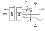
- FIG. 2 is a circuit configuration diagram of the current limiting device shown in FIG. Note that the terminals A, B, and C shown in FIG. 2 correspond to the terminals A, B, and C shown in FIG.
- the current limiting device 3a includes a voltage generation circuit 31, an overcurrent protection circuit 32, FETs (Field Effect Transistors) 33 and 35, and diodes 34 and 36.
- the voltage generation circuit 31 converts the power supply voltage supplied from the terminal Ha into a predetermined voltage set in advance, applies the voltage V GS1 between the gate and the source of the FET 33 via the overcurrent protection circuit 32, and the gate of the FET 35 -Apply the voltage VGS2 between the sources.
- An ON signal or an OFF signal is input to the terminal C connected to the voltage generation circuit 31 from the control unit 5 (see FIG. 3). Details of the voltage generation circuit 31 will be described later.
- the overcurrent protection circuit 32 is a circuit for preventing overcurrent from flowing through the FETs 33 and 35. Details of the overcurrent protection circuit 32 will be described later. Further, as shown in FIG. 2, an FET 33 and a diode 34 are connected in antiparallel to constitute an antiparallel element unit. Similarly, the FET 35 and the diode 36 are connected in antiparallel to constitute an antiparallel element unit.
- the voltage generation circuit 31 is set so that the gate voltages V GS1 and V GS2 are substantially zero.
- the FETs 11a and 11b are turned off, and the charge / discharge current of the storage battery unit 5 (see FIG. 1) is interrupted.
- the current limiting device 1a has been described above, the current limiting devices 1b,..., 1n have the same configuration.
- FIG. 3 is a characteristic diagram showing the relationship between the drain-source voltage V DS and the drain current I DS of the FET.
- the horizontal axis represents the drain-source voltage V DS
- the vertical axis represents the drain current I DS .
- the drain-source voltage V DS and the drain current are within the range of V DS ⁇ V GS -V th.
- relationship between the I DS is a linear region which is substantially linear.
- the drain-source voltage V DS is a constant current region where the drain-source voltage V DS is substantially constant even when the drain-source voltage V DS changes.
- the drain current IDS changes as indicated by the up and down arrows in FIG. That is, when the gate voltage V GS is lowered, the drain current I DS is decreased, and when the gate voltage V GS is increased, the drain current I DS is increased. Therefore, when the FET is operated in the constant current region, if the gate voltage V GS is constant, the drain current I DS hardly changes even if the drain-source voltage V DS changes. Incidentally, when the gate voltage V GS is in a range where V GS ⁇ V th , the operating point of the FET enters the cutoff region (weak inversion region), so that the drain current IDS hardly flows.
- FIG. 4 is a circuit configuration diagram of the storage battery system. Since the storage battery units 2a,..., 2n, the FETs 33 and 35, the diodes 34 and 36, and the control unit 5 have been described with reference to FIGS. 1 and 2, here, the voltage generation circuit 31 and the overcurrent protection circuit 32 are described. This will be described in detail.
- the storage battery units 2a,..., 2n may be collectively referred to as “storage battery unit 2”. The same applies to the current limiting devices 3a,..., 3n.
- the voltage generation circuit 31 includes a DC / DC converter 311 and a photocoupler IC 312.
- the DC / DC converter 311 converts the power supply voltage Vcc supplied via the power supply terminal Ha into a predetermined voltage, and supplies the predetermined voltage to the photocoupler IC 312 from the output terminals Voff and Von.
- the internal common terminal com is connected to the source of the FET 33 and the source of the FET 35.
- the output terminal Voff is a terminal that outputs a predetermined voltage when the FETs 33 and 35 are cut off
- the output terminal Von is a terminal that outputs a predetermined voltage when the FETs 33 and 35 are operated in a constant current region.
- the photocoupler IC 312 includes a photocoupler Q, an amplifier circuit S, a bias voltage generation circuit T, and MOSFETs (Metal-Oxide-Semiconductor Field-Effect Transistors) M1 and M2.
- the photocoupler Q converts an input electrical signal into light and transmits a signal by conducting a light receiving element (not shown) with the light.
- the electric signal is input from the control unit 5 via the wiring 4.
- the amplifier circuit S amplifies the current input from the photocoupler Q and outputs it to the bias voltage generation circuit T.
- the bias voltage generation circuit T generates a bias voltage for appropriately operating the respective MOSFETs (M1, M2).
- the MOSFETs (M1, M2) set the output terminal D to a predetermined potential according to the voltage input from the bias voltage generation circuit T.
- the voltage generation circuit 31 applies a predetermined voltage corresponding to the ON / OFF signal input from the control unit 5 to the FET 33 and the FET 35 via the overcurrent protection circuit 32. More specifically, when the ON signal is input from the control unit 5, the voltage generation circuit 31 has gate voltages V GS1 and V GS2 (for example, V1: substantially equal to each of the FETs 33 and 35). (See FIG. 3).
- charging current flows from the external load (not shown) to the storage battery unit 2a, or the storage battery unit A discharge current flows from 2a to the external load. More specifically, a charging current flows into the storage battery unit 2a from an external load (not shown) through the terminal A, the FET 33, the diode 36, and the terminal B. Further, a discharge current flows out from the storage battery unit 2a to an external load (not shown) through the terminal B, the FET 35, the diode 34, and the terminal A.
- the overcurrent protection circuit 32 includes Zener diodes Z1, Z2, Z3, and Z4 and resistors R1, R2, R3, and R4. Zener diodes Z1 and Z2 are connected in series in opposite directions.
- the resistor R3 has one end connected to the gate of the FET 33 and the other end connected to the output terminal D of the voltage generation circuit 31.
- the resistor R1 is connected in parallel with the Zener diodes Z1 and Z2 between the gate and source of the FET 33, and is connected to the one end of the resistor R3.
- the Zener diodes Z3 and Z4 and the resistors R2 and R4 are for protecting the FET 35 and are connected in the same manner as described above.
- Zener diodes Z1 and Z2 prevent an excessive charge / discharge current from flowing through the FET 33.
- the Zener diodes Z3 and Z4 prevent an excessive charge / discharge current from flowing through the FET 35.
- the resistors R1 and R3 divide the voltage of the output terminal D with respect to the internal common terminal com of the voltage generation circuit 31 so that an appropriate voltage is applied between the gate and the source of the FET 33. As with the resistors R2 and R4, an appropriate voltage is applied between the gate and source of the FET 35 as described above.
- the resistors R3 and R4 are connected to the output terminal D of the voltage generation circuit 31 through a common connection point E.
- the voltage generation circuit 31 and the overcurrent protection circuit 32 included in the current limiting device 3a have been described.
- the current limiting devices 3b, ..., 3n also have the same configuration.
- the wiring 4 connecting the photocoupler IC 312 and the control unit 5 is common to each current limiting device 3.
- the current limiting devices 3b,..., 3n also have the same configuration as the current limiting device 3a.
- the voltages V GS1 and V GS2 (see FIG. 2) based on the potential of the internal common terminal com of the DC / DC converter 31 become the predetermined voltage V ON corresponding to the potential of the terminal D. That is, the voltage V ON is applied as the gate voltage of the FETs 33 and 35. Therefore, in the circuit shown in FIG. 4, when an ON signal is input from the control unit 5 to the photocoupler IC 312, the drain current ID and the drain-source voltage V DS of the FETs 33 and 35 are, for example, shown in FIG. The relationship indicated by the solid line. In this case, since the gate voltages of the FETs 33 and 35 are higher than the threshold voltage Vth , the characteristics of the FETs 33 and 35 are not in the cutoff region.
- the terminal shown in FIG. 2 A when the voltage applied between the B is small, the drain of FET33,35 - for even smaller source voltage V DS, as shown in FIG. 3, the FET33,35 Operates in the linear region.
- the drain-source voltage V DS of the FETs 33 and 35 when the voltage applied between the terminals A and B shown in FIG. 2 is large, the drain-source voltage V DS of the FETs 33 and 35 also increases, so that the FETs 33 and 35 are constant as shown in FIG. Operates in the current domain.
- the drain - even if the source voltage V DS is changed to the voltage V2 from the voltage V1 shown in FIG. 3, the drain current I D is hardly changed.
- the voltage V ON applied to the gates of the FETs 33 and 35 is higher than the threshold voltage V th shown in FIG. 3, and the drain current ID in the constant current region has a desired current value. Is set in advance. Therefore, ON signal is input to the current limiting device 3, the drain of FET33,35 - a source voltage V DS is the voltage value V0 (the voltage value of the boundary between the linear region and the constant current region shown in FIG. 3) or more In such a case, the drain current ID is automatically limited by the characteristics of the FETs 33 and 35.
- a current flows from the external load (not shown) to the storage battery unit 2a via the FET 33 and the diode 36.
- the FET 33 has the above characteristics, the charging current can be limited to a predetermined value or less.
- the discharge current can be limited to a predetermined value or less. Therefore, for example, when a storage battery having a different voltage is newly connected in parallel, a large inrush current can be prevented from flowing into the storage battery 2 due to a voltage difference.
- the charge / discharge current of the storage battery unit 2a can be automatically limited to a predetermined value or less by making use of the characteristics of the FETs 33 and 35.
- the storage battery units 2b,..., 2n and the current limiting devices 3a,..., 3b see FIG. 4).
- the FET 33 and the diode 34 connected in antiparallel and the FET 35 and the diode 36 are connected in series in opposite directions so that current flows in both directions of the current limiting means 3. Therefore, in accordance with charging / discharging of the storage battery unit 2, one of the FETs (FET 33 or FET 35) has a current limiting function.
- the current limiting device 3 If the current limiting device 3 is not provided and the internal resistance of the storage battery unit 2 is different, the charge / discharge current of the storage battery unit 2 with the low internal resistance will reach the rated current first, The storage battery unit 2 having a large resistance cannot reach the rated current.
- the current limiting device 3 since the current limiting device 3 is connected to each storage battery unit 2, it is possible to equalize the voltage between the storage battery units 2 while suppressing excessive cross current. As a result, the rated current can be extracted from each storage battery unit 2, and the maximum charge / discharge current can be obtained for the entire system.
- the charge / discharge current of each storage battery unit 2 can be limited to a predetermined value or less with a simple circuit configuration, and the voltage between the storage battery units 2 can be equalized. .
- the storage battery unit 2 can be protected to enable safe operation, and the maximum charge / discharge power can be obtained for the entire storage battery system.
- a voltage V OFF corresponding to the OFF signal is applied as the gate voltage of the FETs 33 and 35.
- the voltage generating means 31 is set so that the voltage V OFF is lower than the gate-source threshold voltage V th . Accordingly, the FETs 33 and 35 operate in the cut-off region indicated by the oblique lines in FIG. In this case, since the drain current ID does not flow through the FETs 33 and 35, the charge / discharge current of each storage battery unit 2 becomes zero. That is, by operating the FETs 33 and 35 in the cutoff region, the terminals A and B can be electrically cut off, and charging / discharging of each storage battery unit 2 can be stopped.
- FIG. 5 is a circuit configuration diagram of a current limiting device provided in the storage battery system according to the second embodiment of the present invention.
- the storage battery system 100A according to the second embodiment differs from the storage battery system 100 according to the first embodiment in the configuration of the current limiting device 3A, but the other configurations are the same as in the case of the first embodiment. It is. Therefore, the current limiting device 3A will be described, and the description of other configurations will be omitted.
- the current limiting device 3A includes a series element unit in which an FET 33 and a diode 34 are connected in series in the forward direction, and a series element unit in which an FET 35 and a diode 36 are connected in series in the forward direction. It has. The two sets of series element units are connected in antiparallel so that current flows in both directions of the current limiting device 4.
- the source of the FET 33 is connected to the anode of the diode 34, the gate is connected to the output terminal D (see FIG. 4) of the voltage generation circuit 31 via the overcurrent protection circuit 32, and the drain is connected to the terminal A.
- the cathode of the diode 34 is connected to the terminal B.
- the source of the FET 35 is connected to the anode of the diode 36, the gate is connected to the output terminal D (see FIG. 4) of the voltage generation circuit 31 via the overcurrent protection circuit 32, and the drain is connected to the terminal B. .
- the cathode of the diode 35 is connected to the terminal A. Furthermore, wiring for supplying a gate voltage to be applied to the FETs 33 and 35 from the voltage generation circuit 31 is provided.
- FIG. 6 is a circuit configuration diagram of a current limiting device provided in the storage battery system according to the third embodiment of the present invention. Note that the storage battery system 100B according to the third embodiment is different in the arrangement of the FET 33 and the diode 34 from the storage battery system 100 according to the second embodiment.
- the drain of the FET 33 is connected to the cathode of the diode 34, the gate is connected to the output terminal D (see FIG. 4) of the voltage generation circuit 31 via the overcurrent protection circuit 32, and the source is the terminal B. It is connected to the.
- the anode of the diode 34 is connected to the terminal A.
- the drain of the FET 35 is connected to the cathode of the diode 36, the gate is connected to the output terminal D (see FIG. 4) of the voltage generation circuit 31 via the overcurrent protection circuit 32, and the source is connected to the terminal A. Yes.
- the anode of the diode 36 is connected to the terminal B. Furthermore, wiring for applying a gate voltage from the voltage generation circuit 31 to the FETs 33 and 35 is provided.
- FIG. 7 is a circuit configuration diagram of a storage battery system according to the fourth embodiment of the present invention.
- the storage battery system 100 according to the first embodiment has a configuration in which each current limiting device 3 includes a voltage generation circuit 31 (see FIG. 4), but the storage battery system 100C according to the fourth embodiment includes each current limiting device. 30 (30a,..., 30n) is not provided with the voltage generation circuit 31.
- the storage battery system 100C according to the fourth embodiment has a configuration including a control device 50 including a voltage generation circuit 31 and a control unit 51. Since other configurations are the same as those in the first embodiment, description thereof is omitted.
- the control device 50 includes a voltage generation device 31 having a DC / DC converter 311 and a photocoupler IC 312, and a control unit 5.
- the output terminal D of the voltage generation device 31 is connected to each current limiting device 30 via the wiring 4.
- each current limiting device 30 includes an overcurrent protection circuit 32 connected to the output terminal D of the voltage generation device 31, FETs 33 and 35, and diodes 34 and 36.
- the connection relationship between the overcurrent protection circuit 32, the FETs 33 and 35, and the diodes 34 and 36 is the same as that of the storage battery system 100 according to the first embodiment, and thus the description thereof is omitted.
- FIG. 8 is a circuit configuration diagram of a storage battery system according to the fifth embodiment of the present invention.
- the DC / DC converter includes the voltage control terminal Vctrl, and the control unit 5 sends the voltage control signal to the voltage control terminal Vctrl.
- the input is different.
- the storage battery system 100D is different in that the photocoupler IC 312 (see FIG. 4) is not provided. Since other configurations are the same as those in the first embodiment, description thereof is omitted.
- a control terminal Vctrl included in the DC / DC converter 310 illustrated in FIG. 8 is connected to the control unit 5.
- the DC / DC converter 310 converts the power supply voltage Vcc into a predetermined voltage corresponding to the voltage control signal input from the control unit 5, and converts the predetermined voltage from the output terminal Vout through the overcurrent protection circuit 32 to the FET 33, Applied between 35 gate-sources.
- the internal common terminal com of the DC / DC converter 310 is connected to the source of the FET 33 and the source of the FET 35.
- the controller 5 adjusts the input voltage to the current limiting device 40 (that is, the gate voltage of the FETs 33 and 34) by outputting a voltage control signal to the voltage control terminal Vctrl of the DC / DC converter 310. ing.
- the gate voltages of the FETs 33 and 34 change according to the voltage control signal input from the control unit 5 to the voltage control terminal Vctrl.
- the limit value of the discharge current can be changed to an arbitrary level (see FIG. 3). Therefore, the magnitude of the charge / discharge current can be changed according to the state of the storage battery unit 2 such as the battery capacity and internal resistance. For example, when the battery capacity (remaining capacity) of the storage battery unit 2 decreases, the charge / discharge current of the storage battery unit can be reduced by reducing the gate voltage VGS .
- FIG. 9 is a circuit configuration diagram of a storage battery system according to the sixth embodiment of the present invention.
- the storage battery system 100E according to the present embodiment is different from the storage battery system 100 according to the first embodiment in that a monitoring unit 6 that monitors the current, voltage, or temperature of the current limiting device 3 is added. Since other configurations are the same as those in the first embodiment, description thereof is omitted.
- the monitoring unit 6 monitors the temperature and current of the current limiting device 3 and the control unit 5 controls the limiting current value based on the temperature and current will be described.
- the storage battery system 100E includes a storage battery unit 2, a current limiting device 3, temperature sensors Ta, Tb,..., Tn, current sensors Aa, Ab,.
- the unit 6 and the control unit 5 are provided.
- the storage battery unit 2 and the current limiting device 3 since it is the same as that of the storage battery system 100 which concerns on 1st Embodiment, description is abbreviate
- the temperature sensor Ta is installed in the current limiting device 3a, detects the temperature of the current limiting device 3a, and outputs it to the monitoring unit 6. The same applies to the temperature sensors Tb, ..., Tn.
- the voltage sensor Aa is connected in series to the current limiting device 3a, detects the current flowing through the current limiting device 3a, and outputs it to the monitoring unit 6. The same applies to the current sensors Ab, ..., An.
- the monitoring unit 6 includes electronic circuits (not shown) such as a CPU, a ROM, a RAM, and various interfaces, and the control unit 5 according to detection values input from the temperature sensor T and the current sensor A.
- a limit current value reduction instruction signal, an increase instruction signal, or a current interruption instruction signal is output.
- the control unit 5 controls the gate voltage (that is, the limit current value: see FIG. 3) of each current limiting device 3 in accordance with each signal input from the monitoring unit 6.
- FIG. 10 is a flowchart showing a flow of monitoring control performed by the storage battery system according to the sixth embodiment.
- the monitoring unit 6 determines whether or not the temperature of the current limiting device 3 input from the temperature sensor T is equal to or higher than a predetermined temperature Ta.
- the predetermined temperature Ta is a temperature when charging / discharging of the storage battery unit 2 is performed at substantially the rated current, and is a preset temperature (for example, 60 ° C.).
- the process of the monitoring unit 6 proceeds to step S2.
- the process of the monitoring unit 6 proceeds to step S5.
- step S2 the monitoring unit 6 determines whether or not the temperature of the current limiting device 3 input from the temperature sensor T is equal to or higher than a predetermined temperature Tb.
- the predetermined temperature Tb is a threshold value for the safe operation of the storage battery system 100E, and is a preset temperature (for example, 100 ° C.).
- the process of the monitoring unit 6 proceeds to step S3.
- the process of the monitoring unit 6 proceeds to step S4.
- step S ⁇ b> 3 the monitoring unit 6 outputs a current interruption instruction signal to the control unit 5. This is because the current limiting device 3 operates at a high temperature exceeding the safe temperature range.
- the control part 5 operates FET33,35 with which the electric current limiting apparatus 3 is equipped in an interruption
- step S ⁇ b> 4 the monitoring unit 6 outputs a limit current value reduction instruction signal to the control unit 5. That is, although the current limiting device 3 operates within a safe temperature range, since the temperature is relatively high (that is, a current close to the rated current flows), the charge / discharge current of the storage battery unit 2 is reduced. Reduce. Note that when the limit current value reduction instruction signal is input from the monitoring unit 6, the control unit 5 decreases the gate voltage applied to the FETs 33 and 35 by a predetermined voltage (for example, 25 mV) set in advance. Then, the current limit value of the current limiting device 3 is reduced in response to the decrease in the gate voltage (see FIG. 3).
- a predetermined voltage for example, 25 mV
- step S ⁇ b> 5 the monitoring unit 6 determines whether the current limiting device 3 is operating at the rated current based on the current value input from the current sensor A. Note that the value of the rated current is stored in advance in storage means (not shown) of the monitoring unit 6. When the current limiting device 3 is operating at the rated current (step S5 ⁇ Yes), the process of the monitoring unit 6 returns to step S1. When the current limiting device 3 is not operating at the rated current, that is, when it is operating below the rated current (step S5 ⁇ No), the process of the monitoring unit 6 proceeds to step S6.
- step S ⁇ b> 6 the monitoring unit 6 outputs a limit current value increase instruction signal to the control unit 5. This is because the current value flowing through the current limiting device 3 does not reach the rated current, and there is no problem even if the limited current value is increased by a predetermined amount.
- a limit current value increase instruction signal is input from the monitoring unit 6, the control unit 5 increases the gate voltage applied to the FETs 33 and 35 by a predetermined voltage (for example, 25 mV) set in advance. Then, the limit current value of the current limiting device 3 increases corresponding to the increase in the gate voltage (see FIG. 3).
- the control unit 5 when the current limiting device 3 is at a high temperature, the control unit 5 operates the FETs 33 and 35 provided in the current limiting device 3 in the cutoff region. That is, by not charging / discharging the storage battery unit 2, the storage battery system 100E can be safely operated. Further, the control unit 5 controls the gate voltage of the FETs 33 and 35 based on the temperature and current of each current limiting device 3 input from the monitoring unit 6, so that the maximum charge of the entire system within the safe operating range is achieved. A discharge current can be obtained.
- FIG. 11 is a circuit configuration diagram of a storage battery system according to a seventh embodiment of the present invention.
- the storage battery system 100F according to the seventh embodiment is different from the storage battery system 100 according to the first embodiment in that the current limiting device 50 includes six sets of anti-parallel connection units of FETs and diodes. Since other configurations are the same as those of the storage battery system 100 according to the first embodiment, description thereof is omitted.
- an antiparallel element unit in which an FET 33p and a diode 34p are connected in antiparallel and an antiparallel element unit in which an FET 35p and a diode 36p are connected in antiparallel are connected in series. It is connected.
- the FETs 33q and 35q and the diodes 34q and 36q, and the FETs 33r and 35r and the diodes 34r and 36r have the same configuration as described above.
- three sets of antiparallel element units connected in series are further connected in parallel. That is, in the storage battery system 100F according to the present embodiment, there are three charging paths or discharging paths.
- a FET operating in a constant current region generates heat because a drain current flows in a state where a voltage is applied between the drain and the source.
- the charge / discharge current is divided by increasing the number of FETs to have three charge / discharge paths, and the heat generated by the current flow can be distributed to each FET. it can. That is, by having a plurality of charging / discharging paths, it is possible to secure a charging / discharging current necessary for the storage battery system while suppressing the amount of heat generated from each FET and diode.
- FIG. 12 is a circuit configuration diagram of a storage battery system according to the eighth embodiment of the present invention.
- the storage battery system 100G according to the eighth embodiment has the control unit 5 configured to connect the current limiting devices 3a and 3b via the wires 4a, 4b,. ,..., 3n are individually controlled.
- the other points are the same as in the case of the first embodiment, and thus the description thereof is omitted.
- the control unit 5 and the current control devices 3a, 3b,... 3n are connected via wirings 4a, 4b,.
- the wiring 4 a is connected to the input terminal of the photocoupler IC 312 provided in the voltage generation circuit 31.
- the wirings 4b,..., 4n are the same as described above.
- the charging / discharging current of the storage battery unit 2 can be interrupted by outputting an OFF signal to the current limiting device 3 corresponding to the deteriorated storage battery unit 2. it can.
- an ON signal can be continuously output to the current limiting device 3 corresponding to the normal storage battery unit 2. Therefore, the maintenance and replacement of the specific storage battery unit 2 can be performed while continuing the operation of the storage battery system 100G.
- the embodiment of this invention is not limited to these description, A various change etc. can be performed.
- the semiconductor element included in the current control device 3 may be a semiconductor element having constant current characteristics, such as a bipolar transistor or IGBT (Insulated Gate Bipolar Transistor).
- the external power supply terminal 28 for supplying the power supply voltage can be shared by each current limiting device 3 instead of being provided individually by each current limiting device 3.
- the resistances R1, R2, R3, and R4 (see FIG. 4) for adjusting the gate voltage applied to the gates of the FETs 33 and 35 may be changed for each current limiting device 3. .
- the storage battery systems described in the first to eighth embodiments can be appropriately combined.
- the current limiting device 3A shown in FIG. 5 or the current limiting device 3B shown in FIG. 6 may be applied to the storage battery system 100C shown in FIG.
- the monitoring unit 6 outputs a predetermined signal to the control unit 5 based on the detection values input from the temperature sensor T and the current sensor A.
- the temperature sensor T may be installed in the current limiting device 3 and the current sensor A may not be installed.
- the monitoring unit 6 based on the detection value input from the temperature sensor T, the monitoring unit 6 performs, for example, the processes of steps S1 to S4 shown in FIG.
- the current sensor A and the voltage sensor V may be installed in the current limiting device 3 and the temperature sensor T may not be provided. Since the temperature of the current limiting device 3 is proportional to the power consumed by the current limiting device 3 (that is, the product of current and voltage), the monitoring unit 6 is based on the detection values input from the current sensor A and the voltage sensor V. Then, the temperature of the current limiting device may be estimated and the same control as that shown in FIG. 10 may be performed. In the sixth embodiment, the temperature sensor T or the current sensor A is installed in the current limiting device 3, but the present invention is not limited to this. That is, the temperature sensor T or the voltage sensor V may be installed in the storage battery unit 2.
- the storage battery unit 2 has been described as a configuration in which the cells are connected in series, but the present invention is not limited to this.
- the storage battery unit may be a unit in which single cells are connected in parallel, or a unit in which a plurality of single cells are connected in series is connected in parallel.
- the control unit 5 controls ON / OFF of the current limiting device 3.
- the control unit 5 is omitted and the voltage generation circuit 31 supplies the FETs 33 and 35 with a predetermined value. The gate voltage may be applied.
Landscapes
- Engineering & Computer Science (AREA)
- Power Engineering (AREA)
- Manufacturing & Machinery (AREA)
- Chemical & Material Sciences (AREA)
- Chemical Kinetics & Catalysis (AREA)
- Electrochemistry (AREA)
- General Chemical & Material Sciences (AREA)
- Secondary Cells (AREA)
- Charge And Discharge Circuits For Batteries Or The Like (AREA)
Abstract
La présente invention porte sur un système de batterie de stockage dans lequel des fonctionnements sûrs peuvent être réalisés, tout en maintenant une performance de chargement/déchargement. Un système de batterie de stockage (100) a une pluralité de modules de batterie de stockage (1) reliés en parallèle, chacun desdits modules de batterie de stockage comportant une unité de batterie de stockage (2) ayant une pluralité de batteries unitaires, et un moyen de limitation de courant (3) relié en série à l'unité de batterie de stockage (2). Le moyen de limitation de courant (3) comporte : des éléments semi-conducteurs (33, 35) ; et un moyen d'application de tension (31, 32), qui limite un courant de charge/décharge de l'unité de batterie de stockage (2) par l'intermédiaire des éléments semi-conducteurs (33, 35) à une valeur de courant limite ou inférieure qui correspond à une région de courant constant des éléments semi-conducteurs (33, 35) par application d'une tension prédéterminée aux éléments semi-conducteurs (33, 35).
Priority Applications (2)
| Application Number | Priority Date | Filing Date | Title |
|---|---|---|---|
| PCT/JP2011/077262 WO2013076877A1 (fr) | 2011-11-25 | 2011-11-25 | Système de batterie de stockage |
| EP11870830.4A EP2629392A1 (fr) | 2011-11-25 | 2011-11-25 | Système de batterie de stockage |
Applications Claiming Priority (1)
| Application Number | Priority Date | Filing Date | Title |
|---|---|---|---|
| PCT/JP2011/077262 WO2013076877A1 (fr) | 2011-11-25 | 2011-11-25 | Système de batterie de stockage |
Publications (1)
| Publication Number | Publication Date |
|---|---|
| WO2013076877A1 true WO2013076877A1 (fr) | 2013-05-30 |
Family
ID=48469353
Family Applications (1)
| Application Number | Title | Priority Date | Filing Date |
|---|---|---|---|
| PCT/JP2011/077262 WO2013076877A1 (fr) | 2011-11-25 | 2011-11-25 | Système de batterie de stockage |
Country Status (2)
| Country | Link |
|---|---|
| EP (1) | EP2629392A1 (fr) |
| WO (1) | WO2013076877A1 (fr) |
Cited By (13)
| Publication number | Priority date | Publication date | Assignee | Title |
|---|---|---|---|---|
| JP2015050813A (ja) * | 2013-08-30 | 2015-03-16 | ミツミ電機株式会社 | 電池保護回路、電池保護装置及び電池パック、並びに電池保護方法 |
| KR20160078991A (ko) * | 2013-10-27 | 2016-07-05 | 꼼미사리아 아 레네르지 아또미끄 에 오 에네르지 알떼르나띠브스 | 병렬로 복수의 배터리를 포함하는 전원의 외부 단락으로부터의 보호 |
| JP2017005779A (ja) * | 2015-06-04 | 2017-01-05 | パナソニックIpマネジメント株式会社 | 電源装置、及び、電源装置の動作方法 |
| JP2017538390A (ja) * | 2015-02-24 | 2017-12-21 | エルジー・ケム・リミテッド | バッテリー装置 |
| WO2018012471A1 (fr) * | 2016-07-11 | 2018-01-18 | 株式会社デンソー | Dispositif de commande d'alimentation électrique et système d'alimentation électrique |
| JP2018082577A (ja) * | 2016-11-17 | 2018-05-24 | 喜治 植木 | 電池システム |
| WO2019085233A1 (fr) * | 2017-10-31 | 2019-05-09 | 深圳易马达科技有限公司 | Dispositif d'alimentation électrique son circuit de protection de batterie |
| WO2019146520A1 (fr) * | 2018-01-26 | 2019-08-01 | Necエナジーデバイス株式会社 | Dispositif de commande de batterie, bloc-batterie, procédé de commande de batterie et programme |
| CN111224442A (zh) * | 2020-01-19 | 2020-06-02 | 卧龙电气驱动集团股份有限公司 | 一种支持双向限流的锂电池管理系统 |
| US10693198B2 (en) | 2015-06-30 | 2020-06-23 | Gs Yuasa International Ltd. | Controller, energy storage apparatus, energy storage system, moving object, backup power supply, and controller method |
| US10790679B2 (en) | 2014-09-26 | 2020-09-29 | Mitsumi Electric Co., Ltd. | Battery protection circuit and device, battery pack, and battery protection method |
| WO2023276838A1 (fr) * | 2021-06-29 | 2023-01-05 | パナソニックIpマネジメント株式会社 | Système d'alimentation électrique de secours, objet mobile, procédé de commande de système d'alimentation électrique de secours et programme |
| WO2024070194A1 (fr) * | 2022-09-26 | 2024-04-04 | 日立Astemo株式会社 | Appareil de commutation de source d'alimentation électrique, appareil de commande de véhicule et procédé de commutation de source d'alimentation électrique |
Families Citing this family (3)
| Publication number | Priority date | Publication date | Assignee | Title |
|---|---|---|---|---|
| US11431178B2 (en) | 2018-10-30 | 2022-08-30 | Samsung Sdi Co., Ltd. | Battery system |
| EP3648286A1 (fr) * | 2018-10-30 | 2020-05-06 | Samsung SDI Co., Ltd. | Système de batterie |
| RU2727959C1 (ru) * | 2019-10-08 | 2020-07-28 | Общество С Ограниченной Ответственностью "Тээмп Производство" | Способ управления работой составного твердотельного электрохимического источника постоянного тока |
Citations (6)
| Publication number | Priority date | Publication date | Assignee | Title |
|---|---|---|---|---|
| JPS63265528A (ja) * | 1986-12-02 | 1988-11-02 | Fujitsu Ltd | バツテリ充電回路 |
| JP2002542748A (ja) * | 1999-04-14 | 2002-12-10 | テレフオンアクチーボラゲット エル エム エリクソン(パブル) | 電池充電用の電圧/電流調整器及び方法 |
| JP2003079058A (ja) * | 2001-09-04 | 2003-03-14 | Matsushita Electric Ind Co Ltd | 電池パック |
| JP2006345660A (ja) * | 2005-06-09 | 2006-12-21 | Sony Corp | 電源装置 |
| JP2007166715A (ja) * | 2005-12-09 | 2007-06-28 | Sony Corp | 電池パック及び電池パックの充電方法 |
| JP2010029015A (ja) | 2008-07-23 | 2010-02-04 | Mitsubishi Heavy Ind Ltd | 組電池システム |
-
2011
- 2011-11-25 WO PCT/JP2011/077262 patent/WO2013076877A1/fr active Application Filing
- 2011-11-25 EP EP11870830.4A patent/EP2629392A1/fr not_active Withdrawn
Patent Citations (6)
| Publication number | Priority date | Publication date | Assignee | Title |
|---|---|---|---|---|
| JPS63265528A (ja) * | 1986-12-02 | 1988-11-02 | Fujitsu Ltd | バツテリ充電回路 |
| JP2002542748A (ja) * | 1999-04-14 | 2002-12-10 | テレフオンアクチーボラゲット エル エム エリクソン(パブル) | 電池充電用の電圧/電流調整器及び方法 |
| JP2003079058A (ja) * | 2001-09-04 | 2003-03-14 | Matsushita Electric Ind Co Ltd | 電池パック |
| JP2006345660A (ja) * | 2005-06-09 | 2006-12-21 | Sony Corp | 電源装置 |
| JP2007166715A (ja) * | 2005-12-09 | 2007-06-28 | Sony Corp | 電池パック及び電池パックの充電方法 |
| JP2010029015A (ja) | 2008-07-23 | 2010-02-04 | Mitsubishi Heavy Ind Ltd | 組電池システム |
Cited By (19)
| Publication number | Priority date | Publication date | Assignee | Title |
|---|---|---|---|---|
| JP2015050813A (ja) * | 2013-08-30 | 2015-03-16 | ミツミ電機株式会社 | 電池保護回路、電池保護装置及び電池パック、並びに電池保護方法 |
| KR20160078991A (ko) * | 2013-10-27 | 2016-07-05 | 꼼미사리아 아 레네르지 아또미끄 에 오 에네르지 알떼르나띠브스 | 병렬로 복수의 배터리를 포함하는 전원의 외부 단락으로부터의 보호 |
| JP2016537960A (ja) * | 2013-10-27 | 2016-12-01 | コミサリア ア レネルジ アトミク エ オウ エネルジ アルタナティヴ | 電気装置 |
| KR102279970B1 (ko) | 2013-10-27 | 2021-07-21 | 꼼미사리아 아 레네르지 아또미끄 에 오 에네르지 알떼르나띠브스 | 병렬로 복수의 배터리를 포함하는 전원의 외부 단락으로부터의 보호 |
| US10790679B2 (en) | 2014-09-26 | 2020-09-29 | Mitsumi Electric Co., Ltd. | Battery protection circuit and device, battery pack, and battery protection method |
| US10348107B2 (en) | 2015-02-24 | 2019-07-09 | Lg Chem, Ltd. | Battery device |
| JP2017538390A (ja) * | 2015-02-24 | 2017-12-21 | エルジー・ケム・リミテッド | バッテリー装置 |
| JP2017005779A (ja) * | 2015-06-04 | 2017-01-05 | パナソニックIpマネジメント株式会社 | 電源装置、及び、電源装置の動作方法 |
| US10693198B2 (en) | 2015-06-30 | 2020-06-23 | Gs Yuasa International Ltd. | Controller, energy storage apparatus, energy storage system, moving object, backup power supply, and controller method |
| JP2018011372A (ja) * | 2016-07-11 | 2018-01-18 | 株式会社デンソー | 電源制御装置、及び電源システム |
| WO2018012471A1 (fr) * | 2016-07-11 | 2018-01-18 | 株式会社デンソー | Dispositif de commande d'alimentation électrique et système d'alimentation électrique |
| JP2018082577A (ja) * | 2016-11-17 | 2018-05-24 | 喜治 植木 | 電池システム |
| WO2019085233A1 (fr) * | 2017-10-31 | 2019-05-09 | 深圳易马达科技有限公司 | Dispositif d'alimentation électrique son circuit de protection de batterie |
| WO2019146520A1 (fr) * | 2018-01-26 | 2019-08-01 | Necエナジーデバイス株式会社 | Dispositif de commande de batterie, bloc-batterie, procédé de commande de batterie et programme |
| JPWO2019146520A1 (ja) * | 2018-01-26 | 2021-01-28 | 株式会社エンビジョンAescエナジーデバイス | 電池制御装置、電池パック、電池制御方法、およびプログラム |
| JP7425607B2 (ja) | 2018-01-26 | 2024-01-31 | 株式会社Aescジャパン | 電池制御装置、電池パック、電池制御方法、およびプログラム |
| CN111224442A (zh) * | 2020-01-19 | 2020-06-02 | 卧龙电气驱动集团股份有限公司 | 一种支持双向限流的锂电池管理系统 |
| WO2023276838A1 (fr) * | 2021-06-29 | 2023-01-05 | パナソニックIpマネジメント株式会社 | Système d'alimentation électrique de secours, objet mobile, procédé de commande de système d'alimentation électrique de secours et programme |
| WO2024070194A1 (fr) * | 2022-09-26 | 2024-04-04 | 日立Astemo株式会社 | Appareil de commutation de source d'alimentation électrique, appareil de commande de véhicule et procédé de commutation de source d'alimentation électrique |
Also Published As
| Publication number | Publication date |
|---|---|
| EP2629392A1 (fr) | 2013-08-21 |
Similar Documents
| Publication | Publication Date | Title |
|---|---|---|
| WO2013076877A1 (fr) | Système de batterie de stockage | |
| US9124103B2 (en) | Electrical storage apparatus | |
| US8084997B2 (en) | Voltage sensor module and voltage monitoring apparatus | |
| TWI474172B (zh) | 垂直匯流排電路、電池管理系統以及致能信號傳輸之方法 | |
| KR101733811B1 (ko) | 전지 팩 | |
| US20070188149A1 (en) | Battery voltage monitoring apparatus | |
| JP2010029015A (ja) | 組電池システム | |
| KR20120104500A (ko) | 충방전 제어 회로 및 배터리 장치 | |
| US10700536B2 (en) | Control device, balance correcting system, electric storage system and device | |
| KR101222248B1 (ko) | 배터리 팩 | |
| JP6245516B2 (ja) | 電圧検出装置 | |
| JP2012079083A (ja) | 電流制御回路 | |
| JP5463324B2 (ja) | 組電池システム | |
| US9112408B2 (en) | Provision of an output voltage from a wide range variable and low input voltage | |
| KR20140104378A (ko) | 스위치 회로, 반도체 장치 및 배터리 장치 | |
| EP2814157B1 (fr) | Circuit et système d'alimentation électrique, et dispositif de stockage électrique | |
| JP2013228373A (ja) | 電池監視システム及び半導体装置 | |
| JP2019103318A (ja) | 充放電制御装置、及びバッテリ装置 | |
| US10686323B2 (en) | Charge/discharge control circuit and battery device including the same | |
| JP2011250609A (ja) | 半導体装置 | |
| JP2013207861A (ja) | 充放電回路 | |
| JP6718109B2 (ja) | 過電圧保護回路及び過電圧保護制御方法 | |
| JPWO2013076877A1 (ja) | 蓄電池システム | |
| EP3242390B1 (fr) | Appareil de commande de courant pour sous-module de convertisseur mmc | |
| CN105552453B (zh) | 半导体装置以及电池监视系统 |
Legal Events
| Date | Code | Title | Description |
|---|---|---|---|
| ENP | Entry into the national phase |
Ref document number: 2012554152 Country of ref document: JP Kind code of ref document: A |
|
| WWE | Wipo information: entry into national phase |
Ref document number: 2011870830 Country of ref document: EP |
|
| 121 | Ep: the epo has been informed by wipo that ep was designated in this application |
Ref document number: 11870830 Country of ref document: EP Kind code of ref document: A1 |
|
| NENP | Non-entry into the national phase |
Ref country code: DE |