WO2013069366A1 - 有機薄膜トランジスタ及びその製造方法 - Google Patents
有機薄膜トランジスタ及びその製造方法 Download PDFInfo
- Publication number
- WO2013069366A1 WO2013069366A1 PCT/JP2012/072690 JP2012072690W WO2013069366A1 WO 2013069366 A1 WO2013069366 A1 WO 2013069366A1 JP 2012072690 W JP2012072690 W JP 2012072690W WO 2013069366 A1 WO2013069366 A1 WO 2013069366A1
- Authority
- WO
- WIPO (PCT)
- Prior art keywords
- insulating layer
- gate insulating
- electrode
- film transistor
- organic thin
- Prior art date
- Legal status (The legal status is an assumption and is not a legal conclusion. Google has not performed a legal analysis and makes no representation as to the accuracy of the status listed.)
- Ceased
Links
Images



Classifications
-
- H—ELECTRICITY
- H10—SEMICONDUCTOR DEVICES; ELECTRIC SOLID-STATE DEVICES NOT OTHERWISE PROVIDED FOR
- H10K—ORGANIC ELECTRIC SOLID-STATE DEVICES
- H10K10/00—Organic devices specially adapted for rectifying, amplifying, oscillating or switching; Organic capacitors or resistors having potential barriers
- H10K10/40—Organic transistors
- H10K10/46—Field-effect transistors, e.g. organic thin-film transistors [OTFT]
- H10K10/462—Insulated gate field-effect transistors [IGFETs]
- H10K10/468—Insulated gate field-effect transistors [IGFETs] characterised by the gate dielectrics
- H10K10/471—Insulated gate field-effect transistors [IGFETs] characterised by the gate dielectrics the gate dielectric comprising only organic materials
-
- H—ELECTRICITY
- H10—SEMICONDUCTOR DEVICES; ELECTRIC SOLID-STATE DEVICES NOT OTHERWISE PROVIDED FOR
- H10K—ORGANIC ELECTRIC SOLID-STATE DEVICES
- H10K10/00—Organic devices specially adapted for rectifying, amplifying, oscillating or switching; Organic capacitors or resistors having potential barriers
- H10K10/40—Organic transistors
- H10K10/46—Field-effect transistors, e.g. organic thin-film transistors [OTFT]
- H10K10/462—Insulated gate field-effect transistors [IGFETs]
- H10K10/468—Insulated gate field-effect transistors [IGFETs] characterised by the gate dielectrics
- H10K10/474—Insulated gate field-effect transistors [IGFETs] characterised by the gate dielectrics the gate dielectric comprising a multilayered structure
- H10K10/476—Insulated gate field-effect transistors [IGFETs] characterised by the gate dielectrics the gate dielectric comprising a multilayered structure comprising at least one organic layer and at least one inorganic layer
Definitions
- the present invention relates to a bottom contact type organic thin film transistor using an organic semiconductor and a method of manufacturing the same.
- OLEDs organic electroluminescent diodes
- OFETs organic field effect transistors
- the performance of the organic field effect transistor surpasses the characteristics of the amorphous silicon thin film field effect transistor currently used in many displays, and technological development is carried out to further improve the device characteristics and long-term stability for practical use. ing.
- the gate electrode 2 is formed on the support substrate 1, the gate insulating layer 3 is formed on the gate electrode 2, and the source electrode 6 and the drain are formed on the gate insulating layer 3.
- Bottom contact type in which the electrode 7 is formed and the organic semiconductor layer 8 is formed on the source electrode 6 and the drain electrode 7 or after the organic semiconductor layer 8 is formed on the gate insulating layer 3 as shown in FIG.
- the bottom contact type organic thin film transistor can apply a known photolithography method or the like to the formation of the source electrode 6 and the drain electrode 7, so that a circuit pattern of high definition and a large area can be easily formed, and the applicability to industry is high. Also, unlike the bottom contact type organic thin film transistor, unlike the top contact type organic thin film transistor, since the organic semiconductor layer 8 is formed after the source electrode 6 and the drain electrode 7 are formed, physical and chemical stress associated with the formation of the electrode It has the advantage that the organic semiconductor material which comprises the organic semiconductor layer 8 is not degraded by this.
- the bottom contact type organic thin film transistor is inferior in transistor performance such as mobility as compared with the top contact type organic thin film transistor.
- the organic semiconductor layer 8 is formed after the source electrode 6 and the drain electrode 7 are formed, and in addition to the crystallinity of the organic semiconductor layer 8 easily deteriorating at the electrode end, When the organic semiconductor layer 8 is formed, it is considered that a large electrical contact resistance intervenes between the electrode and the organic semiconductor layer 8.
- Patent Document 1 discloses between the upper surface of the source electrode and the organic semiconductor layer, and between the upper surface of the drain electrode and the organic semiconductor layer Discloses an organic thin film transistor in which an organic monomolecular film is interposed.
- Patent Document 2 discloses an organic thin film transistor using a laminate of a metal layer surface-modified with an oxide layer and an organic thin film as a source electrode and / or a drain electrode.
- an object of the present invention is to provide a bottom contact type organic thin film transistor excellent in transistor performance and a method of manufacturing the same.
- the organic thin film transistor according to the present invention comprises a gate electrode formed on a supporting substrate, a gate insulating layer formed on the gate electrode, and a source electrode and a drain formed on the gate insulating layer.
- An organic thin film transistor comprising: an electrode; and an organic semiconductor layer formed on the source electrode and the drain electrode directly or through another layer, A recessed groove having a predetermined pattern is formed on the upper surface of the gate insulating layer, and the source electrode and the drain electrode are formed in the recessed groove.
- the gate insulating layer is formed of a polymer insulating layer.
- the gate insulating layer is composed of an inorganic oxide layer and a polymer insulating layer, the inorganic oxide layer is disposed on the gate electrode side, and the polymer is on the organic semiconductor layer side.
- an insulating layer is disposed.
- a self-assembled monolayer is interposed between the gate insulating layer and the organic semiconductor layer.
- the method for producing an organic thin film transistor according to the present invention is A gate insulating layer forming step of forming a gate insulating layer on the gate electrode formed on the supporting substrate; A concave groove forming step of forming a concave groove by transferring the pattern shape of the mold to the upper surface of the gate insulating layer by bringing a mold in which a desired pattern is formed into pressure contact with the gate insulating layer while heating.
- the gate insulating layer is formed using a polymer insulating material in the gate insulating layer forming step.
- a polymer insulating material is used on the inorganic oxide layer to form a polymer
- an insulating layer is formed to form the gate insulating layer.
- the source electrode and the drain electrode are formed in the groove formed on the upper surface of the gate insulating layer in the source / drain electrode forming step, and then the surface of the gate insulating layer is formed. It is preferable to perform a planarization process.
- an organic semiconductor layer is formed on the self-assembled monolayer. Is preferred.
- the source electrode and the drain electrode are formed in the recessed groove formed on the upper surface of the gate insulating layer, the step between the source electrode and the gate insulating layer, and the drain There is almost no step between the electrode and the gate insulating layer. Therefore, there is no disorder in the crystallinity of the organic semiconductor layer at the electrode end, the electrical contact resistance between the organic semiconductor layer and the electrode decreases, and excellent transistor performance can be obtained.
- the mold having the desired pattern formed thereon is brought into pressure contact with the gate insulating layer while heating, and the pattern shape of the mold is transferred onto the upper surface of the gate insulating layer.
- the source electrode and the drain electrode are formed in the recessed groove, so that the step between the source electrode and the gate insulating layer and the step between the drain electrode and the gate insulating layer Can be almost eliminated. Therefore, the disorder of the crystallinity of the organic semiconductor layer at the electrode end can be suppressed, the electrical contact resistance between the organic semiconductor layer and the electrode can be reduced, and an organic thin film transistor excellent in transistor performance can be manufactured.
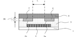
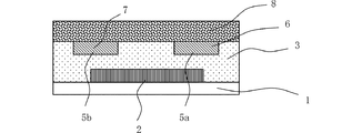
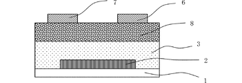
- FIG. 5 is a schematic view of another embodiment of the organic thin film transistor of the present invention. It is the schematic of the modification of the organic thin-film transistor. It is the schematic which shows the gate electrode formation process in the manufacturing method of the organic thin-film transistor of this invention. It is the schematic which shows the gate insulating layer formation process in the manufacturing method of the organic thin-film transistor of this invention. It is the schematic which shows the ditch
- the organic thin film transistor of the present invention has a bottom contact type device structure as shown in FIG.
- the gate electrode 2 is formed on the support substrate 1, and the gate insulating layer 3 is formed on the gate electrode 2.
- the support substrate 1 is not particularly limited as long as it has durability to the process described later.
- Examples include various film substrates such as highly doped Si substrate, glass substrate, PET (polyethylene terephthalate) film, PEN (polyethylene naphthalate) film, PC (polycarbonate) film, PES (polyether sulfone) film, etc. .
- the electrode material of the gate electrode 2 is not particularly limited as long as it has sufficient conductivity to be used as an electrode.
- Various metal materials such as gold, silver, titanium, chromium, nickel and silicon, and conductive oxides such as IZO and ITO can be used.
- the thickness of the gate electrode 2 is not particularly limited. It can be adjusted appropriately depending on the application. For example, 30 to 200 nm is preferable, and 50 to 100 nm is more preferable. If it exceeds 200 nm, the process time tends to be required. If it is less than 30 nm, the wiring resistance tends to increase.
- the gate electrode 2 may not be formed on the support substrate 1 as the support substrate.
- the gate insulating layer 3 is formed of a material having sufficient insulation.
- the gate insulating layer 3 is formed of a polymer insulating layer formed of a polymer insulating material having a glass transition temperature (hereinafter referred to as “Tg”) to form a concave groove.
- Tg glass transition temperature
- the thickness of the gate insulating layer 3 (in this embodiment, the thickness of the polymer insulating layer) is preferably 150 to 1000 nm, and more preferably 200 to 500 nm. If the film thickness of the gate insulating layer is too thin, the insulation tends to be low. When the film thickness of the gate insulating layer is too thick, the capacitance decreases, and the amount of carriers injected into the organic semiconductor layer 8 described later tends to decrease.
- the source electrode concave groove 5 a and the drain electrode concave groove 5 b having a predetermined pattern are formed on the upper surface of the gate insulating layer 3. Then, the source electrode 6 and the drain electrode 7 are formed in each concave groove.
- the distance L between the source electrode recess 5a and the drain electrode recess 5b is the channel length.
- the pattern shape of the concave groove is the pattern shape of the source electrode 6 and the drain electrode 7.
- the pattern shape of the recessed groove can be appropriately changed depending on the application, product and the like.
- the depth H1 of the source electrode concave groove 5a and the drain electrode concave groove 5b is preferably 20 to 100 nm, and more preferably 50 to 100 nm.
- the depth H1 of the recessed groove is large, when the source electrode 6 and the drain electrode 7 are formed in the recessed groove, there is a possibility of leakage between the source electrode 6 and the gate electrode 2.
- the depth H1 of the recessed groove is small, the thickness of the source electrode 6 and the drain electrode 7 tends to be thin. When the thickness of the electrode is reduced, the wiring resistance tends to increase and the current tends not to flow.
- the source electrode 6 and the drain electrode 7 are formed in the recessed groove, the step between the source electrode 6 and the gate insulating layer 3, and the drain electrode 7 and the gate insulating layer 3 There is almost no difference in level. For this reason, the disorder of the crystallinity of the organic semiconductor layer 8 at the electrode end can be suppressed, and the electrical contact resistance between the organic semiconductor layer and the electrode can be further reduced. As shown in the examples described later, the top contact type The mobility and threshold voltage almost equal to those of the organic thin film transistor of the device structure of the above are obtained, and excellent transistor performance is obtained.
- the electrode material of the source electrode 6 and the drain electrode 7 is not particularly limited as long as it has sufficient conductivity to be used as an electrode.
- Various metal materials such as gold, silver, titanium, chromium and nickel can be used.
- the thickness of the source electrode 6 and the drain electrode 7 is the depth of the above-described concave groove.
- the distance (channel length) L between the source electrode 6 and the drain electrode 7 is not particularly limited. For example, 100 micrometers or less are preferable, 50 micrometers or less are more preferable, and 10 micrometers or less are more preferable. According to the present invention, the electrode can be formed even with a fine pattern of 10 ⁇ m or less. By shortening the channel length, high-speed response, high integration of elements, and the like can be achieved.
- the organic semiconductor layer 8 is formed directly on the gate insulating layer 3, the source electrode 6 and the drain electrode 7.
- the organic semiconductor material of the organic semiconductor layer 8 is not particularly limited.
- a conventionally known one can be used.
- P-type low molecular weight organic semiconductor materials such as pentacene and rubrene
- P-type high molecular organic semiconductor materials such as poly-3-hexylthiophene (P3HT)
- P3HT poly-3-hexylthiophene
- n-type organic semiconductor materials such as fullerene
- the film thickness of the organic semiconductor layer 8 is not particularly limited. 10 to 100 nm is preferable, and 20 to 50 nm is more preferable. If it exceeds 100 nm, it takes time to form a film, and the process time tends to increase. If the thickness is less than 10 nm, a film may not be formed (for example, an organic semiconductor is formed in an island shape), and the characteristics may be deteriorated.
- the organic semiconductor layer 8 is directly formed on the gate insulating layer 3, the source electrode 6, and the drain electrode 7.
- the other layer 9 is preferably a self-assembled monolayer or the like.
- a self-assembled monolayer is an organic thin film formed by the spontaneous assembly of organic molecules, and it is a constant formed by the mechanism of the film material itself in a state where fine control from the outside is not added. It is an ultra-thin film such as a monolayer film or LB film having a structure with an order of.
- the self-assembled monolayer can be formed using hexamethyldisilazane (HMDS), octadecyltrichlorosilane (OTS), trichloroperfluororooctylsilane (FOTS) or the like.
- HMDS hexamethyldisilazane
- OTS octadecyltrichlorosilane
- FOTS trichloroperfluororooctylsilane
- the gate insulating layer 3 ′ is composed of an inorganic oxide layer 3 a formed of an inorganic oxide and a polymer insulating layer 3 b formed of a polymer insulating material. Then, the inorganic oxide layer 3 a is disposed on the gate electrode 2 side, and the polymer insulating layer 3 b is disposed on the organic semiconductor layer 8 side. Further, on the upper surface of the polymer insulating layer 3b, the source electrode concave groove 5a and the drain electrode concave groove 5b are formed, and the source electrode 6 and the drain electrode 7 are formed in the concave groove.
- the depth of the recessed groove and the thickness of the gate insulating layer 3' can be easily controlled.
- the inorganic oxide that forms the inorganic oxide layer 3a is formed of a material that has sufficient insulation and that does not deform when the recessed groove is formed on the upper surface of the polymer insulating layer 3b.
- a material that has sufficient insulation and that does not deform when the recessed groove is formed on the upper surface of the polymer insulating layer 3b For example, such SiO 2, Al 2 O 3, Ta 2 O 5 and the like.
- the thickness of the inorganic oxide layer 3a is preferably 100 to 500 nm, and more preferably 100 to 300 nm. If the film thickness of the inorganic oxide layer 3a is too thin, the insulation tends to be low. When the film thickness of the inorganic oxide layer 3 a is too thick, the capacitance decreases, and the amount of carriers injected into the organic semiconductor layer 8 tends to decrease.
- the polymer insulating material for forming the polymer insulating layer 3b is formed of a material having sufficient insulation and having Tg for forming a groove.
- the same polymeric insulating material as that described above can be used.
- the thickness of the polymer insulating layer 3b is preferably 50 to 500 nm, and more preferably 100 to 200 nm.
- a concave groove with a sufficient depth can not be formed, and the source electrode 6 and the drain electrode 7 easily become thin.
- the film thickness of the polymer insulating layer 3b is too thick, the electrostatic capacity decreases, and the amount of carriers injected into the organic semiconductor layer 8 described later tends to be small.
- the depth H2 of the source electrode concave groove 5a and the drain electrode concave groove 5b formed on the upper surface of the polymer insulating layer 3b is preferably 20 to 100 nm, and more preferably 50 to 100 nm.
- the depth H2 of the recessed groove is large, when the source electrode 6 and the drain electrode 7 are formed in the recessed groove, there is a possibility that leakage occurs with the gate electrode 2.
- the depth H2 of the recessed groove is small, the thickness of the source electrode 6 and the drain electrode 7 tends to be thin.
- the film thickness of the gate insulating layer 3 ' (the total film thickness of the inorganic oxide layer 3a and the polymer insulating layer 3b) is preferably 150 to 1000 nm, and more preferably 200 to 500 nm. If it is less than 200 nm, the insulating property tends to be low. When it exceeds 1000 nm, the capacitance decreases and the amount of carriers injected into the organic semiconductor layer 8 tends to decrease.
- the organic semiconductor layer 8 may be formed via another layer 9 such as a self-assembled monolayer.
- the gate electrode 2 is formed on the support substrate 1 (gate electrode formation step).
- the method for forming the gate electrode 2 is not particularly limited. It can form by conventionally well-known methods, such as resistance heating vapor deposition, a sputtering method, an electron beam vapor deposition method, using the electrode material mentioned above.
- the gate electrode forming step can be omitted.
- a gate insulating layer is formed on the surface of the supporting substrate 1 on which the gate electrode 2 is formed, and a gate insulating layer 3 is formed on the gate electrode 2 (gate insulating layer formation Process).
- the gate insulating layer 3 formed of the polymer insulating layer is formed using the above-described polymer insulating material by various coating methods such as spin coating, slit coating, dip coating and the like.
- the mold 4 having the desired pattern formed thereon is brought into pressure contact with the gate insulating layer 3 while heating, and the pattern shape of the mold 4 is transferred onto the upper surface of the gate insulating layer 3 by thermal cycle nanoimprinting.
- the source electrode concave groove 5a and the drain electrode concave groove 5b are formed (a concave groove forming step).
- the mold 4 in which the desired pattern was formed is made to oppose the uneven
- the mold 4 is brought into contact with the gate insulating layer 3 and pressurized.
- the polymer insulating material constituting the gate insulating layer 3 flows to the recess side of the mold 4, and the mold 4 is formed on the upper surface of the gate insulating layer 3.
- the pattern shape of is transferred.
- the heating temperature of the mold 4 is set to be higher than the Tg of the polymer insulating material constituting the gate insulating layer 3. Preferably, it is Tg + 5 ° C. to Tg + 20 ° C., more preferably Tg + 10 ° C. to Tg + 20 ° C. If the heating temperature of the mold 4 is too high, the polymer insulating material constituting the gate insulating layer 3 is likely to be degraded. If the heating temperature is too low, it may not be possible to form the concave groove pattern shape with high accuracy. By setting the heating temperature within the above range, it is possible to enhance the fluidity of the polymeric insulating material to sufficiently flow in the layer, and to prevent deformation of the pattern due to shrinkage upon cooling, which is desired. A pattern-shaped recessed groove can be formed on the upper surface of the gate insulating layer 3.
- the mold 4 is removed from the gate insulating layer 3 after being cooled to Tg ⁇ 20 ° C. or less in a state of being pressurized by the mold 4.
- the source electrode recess 5a and the drain electrode recess 5b to which the pattern shape of the mold 4 is transferred are formed on the upper surface of the gate insulating layer 3.
- the distance between the source electrode recess 5 a and the drain electrode recess 5 b is a channel length, and the length can be made 10 ⁇ m or less by the fine pattern of the mold 4.
- the pattern shape of the recessed grooves 5 a and 5 b is the pattern shape of the source electrode 6 and the drain electrode 7.
- the material of the mold 4 is preferably any material that can withstand heating temperature, has sufficient hardness, and can form a micron shape on the mold surface, and any of quartz, metal, silicon, ceramic, resin, etc. Materials are also applicable.
- the fine pattern can be formed on the mold 4 by etching using, for example, a resist or an inorganic oxide film as a mask. Further, the depth h of the recess of the mold 4 is made smaller than the thickness of the gate insulating layer 3.
- the gate insulating layer 3 and the mold 4 are formed on the surface of the mold 4 so that the pattern portions of the gate insulating layer 3 formed by the mold 4 do not peel together.
- a fluorine coat may be applied to reduce the adhesion of
- the source electrode 6 and the drain electrode 7 are formed in the recess formed in the recess forming step (a source / drain electrode forming step).
- the method of forming the source electrode 6 and the drain electrode 7 is not particularly limited. It can form using the electrode material mentioned above by conventionally well-known methods, such as a mask vapor deposition method (resistance heating vapor deposition method), a sputtering method, an electron beam vapor deposition method, an inkjet method, screen printing, a spin coat method. In the case of coating methods such as inkjet method, screen printing, spin coating method, metal nanoparticle ink such as silver ink can be used.
- the distance (channel length) between the source electrode 6 and the drain electrode 7 is long, for example, when the channel length is 50 ⁇ m or more, it is preferable to form by mask evaporation.
- the source electrode 6 and the drain electrode 7 can be formed in the concave groove on the upper surface of the gate insulating layer 3 without performing surface polishing after electrode formation, and the source electrode 6 and the gate
- the step between the insulating layer 3 and the step between the drain electrode 7 and the gate insulating layer 3 can be 5 nm or less.
- the source electrode 6 and the drain electrode 7 can be formed in the recessed groove on the upper surface of the gate insulating layer 3, and the step between the source electrode 6 and the gate insulating layer 3 and the gate electrode The step between the layer 3 can be eliminated.
- the surface polishing method is not particularly limited.
- the method used for surface polishing of a color filter, a transparent electrode substrate, etc. is applicable.
- CMP chemical mechanical polishing
- the substrate is preferably cleaned.
- the washing can be performed using a suitable detergent or pure water.
- the surface polishing is preferably performed so that the step between the source electrode 6 and the gate insulating layer 3 and the step between the drain electrode 7 and the gate insulating layer 3 are 5 nm or less, more preferably 2 nm or less .
- the disorder of the crystallinity of the organic semiconductor layer 8 at the end portion of the electrode can be suppressed in forming the organic semiconductor layer in the next step.
- the electrical contact resistance between the electrode and the electrode can be made smaller.
- the organic semiconductor layer 8 is formed on the source electrode 6 and the drain electrode 7 (organic semiconductor layer forming step).
- the organic thin film transistor of the present invention can be manufactured.
- the method of forming the organic semiconductor layer 8 is not particularly limited. It can form using the conventionally well-known methods, such as resistance heating vapor deposition and an inkjet method, using the organic-semiconductor material mentioned above.
- the organic semiconductor layer 8 is directly formed on the source electrode 6 and the drain electrode 7 in FIG. 9, the organic semiconductor layer 8 may be formed via another layer such as a self-assembled monolayer.
- a self-assembled monolayer By interposing the self-assembled monolayer, the influence of the interface trap between the gate insulating layer 3 and the organic semiconductor layer 8 can be reduced, and the mobility of electrons can be improved.
- the method of forming a self-assembled monolayer is as follows: hexamethyldisilazane (HMDS), octadecyltrichlorosilane (OTS), trichloroperfluoro on the surface of the gate insulating layer 3 on which the source electrode 6 and the drain electrode 7 are formed. It can be formed by dip coating, spray spraying, or a method of forming a film by evaporating the liquid in high vacuum using a liquid containing rooctylsilane (FOTS) or the like.
- HMDS hexamethyldisilazane
- OTS octadecyltrichlorosilane
- FOTS liquid containing rooctylsilane
- the surfaces of the gate insulating layer 3, the source electrode 6, and the drain electrode 7 can be made hydrophobic, and adsorption of moisture etc. which is the cause of the interface trap
- the mobility of electrons can be improved by preventing.
- the amorphous fluorine resin itself has the same function as the self-assembled monolayer. Since it has, even if it does not form a self-assembled monolayer separately, the same effect as the case where a self-assembled monolayer is formed is acquired.
- the gate electrode forming step is performed in the same manner as the above embodiment to form the gate electrode 2 on the support substrate 1.
- the gate insulating layer 3 ' having a two-layer structure of the inorganic oxide layer 3a and the polymer insulating layer 3b is formed on the gate electrode 2. That is, after the inorganic oxide layer 3a is formed on the gate electrode 2, various applications such as spin coating, slit coating, dip coating, etc. are performed on the inorganic oxide layer 3a using the above-described polymer insulating material.
- the polymer insulating layer 3b is formed by a method.
- the inorganic oxide layer 3a can be formed by sputtering or the like using the above-described inorganic oxide.
- the gate electrode can be formed by thermal oxidation of the metal material of the gate electrode. For example, when the inorganic oxide layer 3a is SiO 2 , it can be formed by thermally oxidizing a doped Si substrate.
- the concave groove forming step is performed, and the pattern shape of the mold 4 is transferred onto the upper surface of the polymer insulating layer 3b of the gate insulating layer 3 'to form the source electrode concave groove 5a and the drain electrode.
- the concave groove 5b is formed.
- the depth h of the recess of the mold 4 is smaller than the film thickness of the polymer insulating layer 3b.
- the source / drain electrode forming step is performed, and the source electrode 6 and the drain electrode 7 are formed in the recess formed in the recess forming step.
- the organic semiconductor layer forming step is performed to form the organic semiconductor layer 8 on the source electrode 6 and the drain electrode 7.
- the organic thin film transistor shown in FIG. 3 can be manufactured.
- Example 1 A 10 mm ⁇ 10 mm ⁇ 0.7 mm thick quartz glass was used as a supporting substrate.
- the quartz glass was mounted on a resistance heating vapor deposition apparatus, and Al was vapor deposited to form a gate electrode with a film thickness of 30 nm.
- a PMMA (polymethyl methacrylate) toluene solution as a polymer insulating material, the polymer insulating material is applied by spin coating on the surface of the supporting substrate on which the gate electrode is formed, and a gate having a film thickness of 500 nm is formed. An insulating layer was formed.
- the supporting substrate is transported to a nanoimprint apparatus, and a mold having a pattern in which two convex portions having dimensions of 100 ⁇ m ⁇ 5000 ⁇ m and depth 50 nm are arranged in a gap of 100 ⁇ m in the lateral direction (corresponding to channel length) is °C heated to a thermal cycle nanoimprinting method performed by pressing at a pressure of 30kgf / cm 2 (2.94MPa (gauge pressure)) to transfer the mold pattern in the gate insulating layer upper surface. Then, while the mold was under pressure, the temperature was lowered to room temperature and cooled to form a recessed groove on the upper surface of the gate insulating layer. The depth of this ditch was 50 nm.
- the mold is removed from the gate insulating layer, and then the supporting substrate is mounted on a resistance heating evaporation apparatus, and 50 nm-thick Au is mask-deposited in the recessed groove formed on the upper surface of the gate insulating layer, Source and drain electrodes were formed. Then, the support substrate is disposed in a resistance heating evaporation apparatus installed in a glove box, and pentacene (made by Aldrich: twice purification by sublimation) is evaporated on the source electrode and the drain electrode to form an organic film with a film thickness of 40 nm. A semiconductor layer was formed to manufacture an organic thin film transistor.
- Example 2 An organic thin film transistor was manufactured in the same manner as in Example 1 except that, in Example 1, an amorphous fluorine resin (trade name "Cytop” manufactured by Asahi Glass) was used as the polymer insulating material instead of the PMMA toluene solution.
- an amorphous fluorine resin trade name "Cytop” manufactured by Asahi Glass
- Example 3 An n-type Si substrate of 10 mm ⁇ 10 mm ⁇ 0.5 mm thickness was used as a support substrate.
- the support substrate functions as a gate electrode.
- the supporting substrate was heated to 800 ° C. and thermally oxidized to form an inorganic oxide layer of 100 nm thick comprising a SiO 2 thin film on the supporting substrate.
- an amorphous fluorine resin (trade name "Cytop” manufactured by Asahi Glass) is applied on the inorganic oxide layer by spin coating to form a polymer insulating layer having a thickness of 50 nm, and the inorganic oxide layer and the polymer insulating layer A gate insulating layer having a two-layer structure was formed.
- Example 2 a thermal cycle nanoimprinting method was performed in the same manner as in Example 1 to form a 50 nm-deep groove only in the portion of the polymer insulating layer. Thereafter, in the same manner as in Example 1, the formation of the source electrode and the drain electrode and the formation of the organic semiconductor layer were performed to manufacture an organic thin film transistor.
- Example 4 A 10 mm ⁇ 10 mm ⁇ 0.7 mm thick quartz glass was used as a supporting substrate.
- the quartz glass was mounted on a resistance heating vapor deposition apparatus, and Al was vapor deposited to form a gate electrode with a film thickness of 30 nm.
- the polymer insulating material was applied by spin coating on the surface of the supporting substrate on which the gate electrode was formed, to form a gate insulating layer with a film thickness of 500 nm. .
- the supporting substrate is transported to a nanoimprint apparatus, and a mold having a pattern in which two convex portions having dimensions of 100 ⁇ m ⁇ 5000 ⁇ m and depth 100 nm are arranged in a gap of 10 ⁇ m in the lateral direction (corresponding to channel length) °C heated to a thermal cycle nanoimprinting method performed by pressing at a pressure of 30kgf / cm 2 (2.94MPa (gauge pressure)) to transfer the mold pattern in the gate insulating layer upper surface. Then, while the mold was under pressure, the temperature was lowered to room temperature and cooled to form a recessed groove on the upper surface of the gate insulating layer. The depth of this ditch was 100 nm.
- the supporting substrate was attached to a resistance heating vapor deposition apparatus, and Au having a film thickness of 100 nm was vapor deposited in the concave groove of the gate insulating layer.
- a foam polyurethane cloth is attached as a polishing pad to a support plate of a polishing machine, and using a chiller in which alumina polishing particles having an average particle diameter of 200 nm are dispersed as a polishing agent, 50 cc per minute of the present polishing agent on the polishing pad.
- the support substrate is disposed in a resistance heating vapor deposition apparatus installed in a glove box, and pentacene (made by Aldrich: sublimation purification is performed twice) is vapor deposited on the self-assembled film to form an organic semiconductor with a film thickness of 40 nm.
- pentacene made by Aldrich: sublimation purification is performed twice
- the layers were formed to produce an organic thin film transistor.
- Example 5 In Example 4, a gate insulating layer with a film thickness of 500 nm was formed using an amorphous fluorine resin (trade name “Cytop” manufactured by Asahi Glass) as a polymer insulating layer material instead of a PMMA toluene solution. Next, a thermal cycle nanoimprinting method was performed in the same manner as in Example 4 to form a recessed groove in the gate insulating layer so as to have a channel length of 10 ⁇ m. Next, in the same manner as in Example 4, source and drain electrodes were formed, and then planarization was performed to form 50 nm of the source and drain electrodes in the concave groove of the gate insulating layer.
- an amorphous fluorine resin trade name “Cytop” manufactured by Asahi Glass
- the support substrate is disposed in a resistance heating vapor deposition apparatus installed in a glove box, and pentacene (made by Aldrich: sublimation purification is performed twice) is vapor deposited on the self-assembled film to form an organic semiconductor with a film thickness of 40 nm.
- pentacene made by Aldrich: sublimation purification is performed twice
- the layers were formed to produce an organic thin film transistor.
- Example 6 An n-type Si substrate of 10 mm ⁇ 10 mm ⁇ 0.5 mm thickness was used as a support substrate.
- the support substrate functions as a gate electrode.
- the supporting substrate was heated to 800 ° C. and thermally oxidized to form an inorganic oxide layer of 100 nm thick comprising a SiO 2 thin film on the supporting substrate.
- an amorphous fluorine resin (trade name "Cytop” manufactured by Asahi Glass) is applied on the inorganic oxide layer by spin coating to form a polymer insulating layer having a thickness of 100 nm, and the inorganic oxide layer and the polymer insulating layer A gate insulating layer having a two-layer structure was formed.
- Example 4 a thermal cycle nanoimprinting method was carried out in the same manner as in Example 4 to form a recessed groove only in the portion of the polymer insulating layer.
- the depth of this ditch was 100 nm.
- the surface is scraped by 50 nm and planarizing treatment is carried out.
- the drain electrode was formed 50 nm.
- a self-assembled film was formed to 1 nm or less.
- the support substrate is disposed in a resistance heating vapor deposition apparatus installed in a glove box, and pentacene (made by Aldrich: sublimation purification is performed twice) is vapor deposited on the self-assembled film to form an organic semiconductor with a film thickness of 40 nm.
- pentacene made by Aldrich: sublimation purification is performed twice
- the layers were formed to produce an organic thin film transistor.
- Comparative Example 1 A 10 mm ⁇ 10 mm ⁇ 0.7 mm thick quartz glass was used as a supporting substrate.
- the quartz glass was mounted on a resistance heating vapor deposition apparatus, and Al was vapor deposited to form a gate electrode with a film thickness of 30 nm.
- the polymer insulating material was applied by spin coating on the surface of the supporting substrate on which the gate electrode was formed, to form a gate insulating layer with a film thickness of 500 nm. .
- the supporting substrate is mounted on a resistance heating vapor deposition apparatus, Au having a channel length of 100 ⁇ m and a film thickness of 50 nm in the same pattern shape as in Examples 1 to 3 is mask deposited, and a source electrode and a drain electrode are formed on the gate insulating layer. Formed. Then, the support substrate is disposed in a resistance heating evaporation apparatus installed in a glove box, pentacene (manufactured by Aldrich: sublimation purification is performed twice) is evaporated to form an organic semiconductor layer having a film thickness of 40 nm, and an organic thin film transistor Manufactured.
- Comparative Example 2 In Comparative Example 1, an organic thin film transistor was manufactured in the same manner as Example 1, except that an amorphous fluorine resin (trade name "Cytop” manufactured by Asahi Glass) was used as the polymer insulating layer material instead of the PMMA toluene solution. .
- an amorphous fluorine resin trade name "Cytop” manufactured by Asahi Glass
- Comparative Example 3 A 10 mm ⁇ 10 mm ⁇ 0.7 mm thick quartz glass was used as a supporting substrate.
- the quartz glass was mounted on a resistance heating vapor deposition apparatus, and Al was vapor deposited to form a gate electrode with a film thickness of 30 nm.
- an amorphous fluorine resin (trade name "Cytop” manufactured by Asahi Glass) is used as the polymer insulating layer material, and the polymer insulating layer material is applied by spin coating to silica glass on which the gate electrode is formed.
- a gate insulating layer was formed.
- pentacene manufactured by Aldrich: sublimation purification was performed twice
- a resistance heating vapor deposition apparatus installed in a glove box
- Au having a channel length of 100 ⁇ m and a film thickness of 50 nm is mask-deposited on the organic semiconductor layer in the same pattern shape as in Examples 1 to 3;
- an organic thin film transistor was manufactured.
- Comparative Example 4 An organic thin film transistor was manufactured in the same manner as in Comparative Example 3 except that the source electrode and the drain electrode were formed to have a channel length of 50 ⁇ m in Comparative Example 3.
- Comparative Example 5 In Comparative Example 3, when the source electrode and the drain electrode were formed with a channel length of 10 ⁇ m, no electrode could be formed.
- the mobility and threshold voltage of the organic thin film transistors of Examples 1 to 6 and Comparative Examples 1 to 5 were measured.
- the mobility and the threshold voltage were determined from the gate voltage-drain current characteristics measured by a semiconductor parameter measurement device (manufactured by Agilent).
- the organic thin film transistors of the present invention of Examples 1 to 6 are superior in mobility to the conventional bottom contact type organic thin film transistors (Comparative Examples 1 and 2), and are top contact type organic thin film transistors The mobility and threshold voltage were the same as in (Comparative Examples 3 to 4).
- the source electrode and the drain electrode are formed in the recessed groove formed on the upper surface of the gate insulating layer, so the step between the source electrode and the gate insulating layer and the drain electrode It is speculated that the difference between the gate insulating layer and the gate insulating layer can be buried to suppress the disorder of the crystallinity at the electrode end, and the large electrical contact resistance between the organic semiconductor layer and the electrode can be resolved. Be done.
- the channel length between the electrodes could not be formed to 10 ⁇ m, but in the organic thin film transistor of the present invention Can be formed, and high-definition pattern formation is possible.
- Support substrate 2 Gate electrode 3, 3 ': Gate insulating layer 3a: Inorganic oxide layer 3b: Polymer insulating layer 4: Mold 4a: Concave and convex pattern 5a: Concave groove 5b for source electrode: Concave groove 6 for drain electrode Source electrode 7: Drain electrode 8: Organic semiconductor layer
Landscapes
- Chemical & Material Sciences (AREA)
- Inorganic Chemistry (AREA)
- Thin Film Transistor (AREA)
Abstract
トランジスタ性能に優れた、ボトムコンタクト型の有機薄膜トランジスタを提供する。 この有機薄膜トランジスタは、支持基板1と、支持基板1上に形成されたゲート電極2と、ゲート電極2上に形成されたゲート絶縁層3と、ゲート絶縁層3上に形成されたソース電極6及びドレイン電極7と、ソース電極6及びドレイン電極7上に直接又は他の層を介して形成された有機半導体層8とを備え、ゲート絶縁層3の上面に所定パターンの凹溝5が形成され、該凹溝5内にソース電極6及びドレイン電極7が形成されている。
Description
本発明は、有機半導体を用いた、ボトムコンタクト型の有機薄膜トランジスタ及びその製造方法に関する。
有機半導体を用いる有機エレクトロニクスは、フレキシブルデバイスなどを製造するための次世代技術として大きく注目されている。すでに製品化された有機電界発光ダイオード(OLED)に加えて、アクティブマトリクス用スイッチング素子を用途とする有機電界効果トランジスタ(OFET)の研究開発が近年大きく進展している。
有機電界効果トランジスタの性能は、現在ディスプレイに多く使用されているアモルファスシリコン薄膜電界効果トランジスタの特性を凌駕しており、実用化に向けデバイス特性と長期安定性をさらに向上させるため技術開発が行われている。
有機薄膜トランジスタのデバイス構造は、図10に示すような、支持基板1上にゲート電極2を形成し、ゲート電極2上にゲート絶縁層3を形成し、ゲート絶縁層3上にソース電極6及びドレイン電極7を形成し、ソース電極6及びドレイン電極7上に有機半導体層8を形成したボトムコンタクト型や、図11に示すような、ゲート絶縁層3上に有機半導体層8を形成した後、有機半導体層8上にソース電極6及びドレイン電極7を形成したトップコンタクト型がある。
ボトムコンタクト型の有機薄膜トランジスタは、ソース電極6及びドレイン電極7の形成に公知のフォトリソグラフィー法等を適用できるので、高精細で大面積の回路パターンを容易に形成でき、産業に対する応用性が高い。また、ボトムコンタクト型の有機薄膜トランジスタは、トップコンタクト型の有機薄膜トランジスタと異なり、ソース電極6及びドレイン電極7を形成した後、有機半導体層8を形成するので、電極形成に伴う物理的、化学的ストレスによって有機半導体層8を構成する有機半導体材料を劣化させないという利点を有する。
しかしながら、ボトムコンタクト型の有機薄膜トランジスタは、トップコンタクト型の有機薄膜トランジスタに比べて、移動度などのトランジスタ性能が劣ることが大きな技術的問題のひとつとされてきた。これは、ソース電極6及びドレイン電極7を形成した後、有機半導体層8を形成するため、電極端部で有機半導体層8の結晶性が悪くなりやすいことに加え、電極である金属の上から有機半導体層8を形成すると、電極と有機半導体層8との間に大きな電気的接触抵抗が介在するためと考えられている。
ボトムコンタクト型の有機薄膜トランジスタのトランジスタ性能を向上させる試みが種々検討されており、例えば、特許文献1には、ソース電極上面と有機半導体層との間、及びドレイン電極上面と有機半導体層との間に、有機単分子膜を介在させた有機薄膜トランジスタが開示されている。また、特許文献2には、酸化物層及び有機薄膜で表面修飾された金属層の積層体を、ソース電極及び/又はドレイン電極として用いた有機薄膜トランジスタが開示されている。
しかしながら、特許文献1や特許文献2に開示された有機薄膜トランジスタであっても、トランジスタ性能は十分ではなかった。
よって、本発明の目的は、トランジスタ性能に優れた、ボトムコンタクト型の有機薄膜トランジスタ及びその製造方法を提供することにある。
上記目的を達成するため、本発明の有機薄膜トランジスタは、支持基板に形成されたゲート電極と、前記ゲート電極上に形成されたゲート絶縁層と、前記ゲート絶縁層上に形成されたソース電極及びドレイン電極と、前記ソース電極及び前記ドレイン電極上に直接又は他の層を介して形成された有機半導体層とを備えた有機薄膜トランジスタであって、
前記ゲート絶縁層の上面に所定パターンの凹溝が形成され、該凹溝内に前記ソース電極及び前記ドレイン電極が形成されていることを特徴とする。
前記ゲート絶縁層の上面に所定パターンの凹溝が形成され、該凹溝内に前記ソース電極及び前記ドレイン電極が形成されていることを特徴とする。
本発明の有機薄膜トランジスタは、前記ゲート絶縁層が、高分子絶縁層で構成されることが好ましい。
本発明の有機薄膜トランジスタは、前記ゲート絶縁層が、無機酸化物層と高分子絶縁層とで構成され、前記ゲート電極側に前記無機酸化物層が配置され、前記有機半導体層側に前記高分子絶縁層が配置されていることが好ましい。
本発明の有機薄膜トランジスタは、前記ゲート絶縁層と前記有機半導体層との間に自己組織化単分子層が介在していることが好ましい。
また、本発明の有機薄膜トランジスタの製造方法は、
支持基板に形成されたゲート電極上にゲート絶縁層を形成するゲート絶縁層形成工程と、
前記ゲート絶縁層に対し、所望のパターンが形成されたモールドを加熱しながら加圧接触させて、前記ゲート絶縁層の上面に前記モールドのパターン形状を転写して凹溝を形成する凹溝形成工程と、
前記凹溝形成工程で形成した凹溝内に、ソース電極及びドレイン電極を形成するソース・ドレイン電極形成工程と、
前記ソース電極及び前記ドレイン電極上に、直接又は他の層を介して有機半導体層を形成する有機半導体層形成工程とを少なくとも備えることを特徴とする。
支持基板に形成されたゲート電極上にゲート絶縁層を形成するゲート絶縁層形成工程と、
前記ゲート絶縁層に対し、所望のパターンが形成されたモールドを加熱しながら加圧接触させて、前記ゲート絶縁層の上面に前記モールドのパターン形状を転写して凹溝を形成する凹溝形成工程と、
前記凹溝形成工程で形成した凹溝内に、ソース電極及びドレイン電極を形成するソース・ドレイン電極形成工程と、
前記ソース電極及び前記ドレイン電極上に、直接又は他の層を介して有機半導体層を形成する有機半導体層形成工程とを少なくとも備えることを特徴とする。
本発明の有機薄膜トランジスタの製造方法は、前記ゲート絶縁層形成工程において、高分子絶縁材料を用いて前記ゲート絶縁層を形成することが好ましい。
本発明の有機薄膜トランジスタの製造方法は、前記ゲート絶縁層形成工程において、無機酸化物を用いて無機酸化物層を形成した後、該無機酸化物層上に、高分子絶縁材料を用いて高分子絶縁層を形成して、前記ゲート絶縁層を形成することが好ましい。
本発明の有機薄膜トランジスタの製造方法は、前記ソース・ドレイン電極形成工程において、前記ゲート絶縁層上面に形成した前記凹溝に前記ソース電極と前記ドレイン電極とを形成した後、前記ゲート絶縁層表面を平坦化処理することが好ましい。
本発明の有機薄膜トランジスタの製造方法は、有機半導体層形成工程において、前記ゲート絶縁層上に自己組織化単分子層を形成した後、該自己組織化単分子層上に有機半導体層を形成することが好ましい。
本発明の有機薄膜トランジスタによれば、ソース電極及びドレイン電極が、ゲート絶縁層の上面に形成された凹溝内に形成されているので、ソース電極とゲート絶縁層との間の段差、及び、ドレイン電極とゲート絶縁層との間の段差が殆どない。このため、電極端部における有機半導体層の結晶性の乱れがなく、有機半導体層と電極との間の電気的接触抵抗が小さくなり、優れたトランジスタ性能が得られる。
また、本発明の有機薄膜トランジスタの製造方法によれば、ゲート絶縁層に対し、所望のパターンが形成されたモールドを加熱しながら加圧接触させて、ゲート絶縁層の上面にモールドのパターン形状を転写して凹溝を形成した後、該凹溝内に、ソース電極及びドレイン電極を形成するので、ソース電極とゲート絶縁層との間の段差、及び、ドレイン電極とゲート絶縁層との間の段差をほぼ無くすことができる。このため、電極端部における有機半導体層の結晶性の乱れを抑制でき、有機半導体層と電極との間の電気的接触抵抗が小さくなり、トランジスタ性能に優れた有機薄膜トランジスタを製造できる。
本発明の有機薄膜トランジスタの一実施形態について説明する。本発明の有機薄膜トランジスタは、図1に示すように、ボトムコンタクト型のデバイス構造をなしている。
すなわち、支持基板1上にゲート電極2が形成され、ゲート電極2上にゲート絶縁層3が形成されている。
支持基板1は、後述するプロセスに対する耐久性を有するものであればよく、特に限定はない。例としては、ハイドープされたSi基板、ガラス基板、PET(ポリエチレンテレフタレート)フィルム、PEN(ポリエチレンナフタレート)フィルム、PC(ポリカーボネート)フィルム、PES(ポリエーテルスルホン)フィルムなどの各種フィルム基板などが挙げられる。
ゲート電極2の電極材料としては、電極として用いるのに十分導電性を有するものであればよく、特に限定はない。金、銀、チタン、クロム、ニッケル、シリコンなどの各種金属材料、IZO、ITOなどの導電性酸化物などを使用できる。
ゲート電極2の厚さは、特に限定は無い。用途により適宜調整できる。例えば、30~200nmが好ましく、50~100nmがより好ましい。200nmを超えると、プロセス時間を要する傾向にある。30nm未満であると、配線抵抗が大きくなる傾向にある。
なお、支持基板として、ハイドープされたSi基板などのように、支持基板自体がゲート電極として機能するものを用いた場合は、支持基板1上にゲート電極2を形成しなくてもよい。
ゲート絶縁層3は、十分な絶縁性を有する材料で形成される。この実施形態では、ゲート絶縁層3は、凹溝形成のため、ガラス転移温度(以下、「Tg」と記す)を有する高分子絶縁材料で形成された高分子絶縁層で構成されている。
高分子絶縁材料の具体例としては、たとえば、PMMA(ポリメチルメタクリレート、Tg=105℃)、PVP(ポリビニルフェノール、Tg=146℃)、PVA(ポリビニルアルコール、Tg=85℃)、アモルファスフッ素樹脂などの高分子材料などが挙げられる。アモルファスフッ素樹脂としては、旭硝子株式会社から市販されている、「Cytop」(商品名、Tg=108℃)などが挙げられる。
ゲート絶縁層3の膜厚(この実施形態では、高分子絶縁層の膜厚)は、150~1000nmが好ましく、200~500nmがより好ましい。ゲート絶縁層の膜厚が薄すぎると絶縁性が低くなる傾向にある。ゲート絶縁層の膜厚が厚すぎると静電容量が小さくなり、後述する有機半導体層8に注入されるキャリア量が少なくなる傾向にある。
本発明の有機薄膜トランジスタは、ゲート絶縁層3の上面に、所定パターンのソース電極用凹溝5a及びドレイン電極用凹溝5bが形成されている。そして、各凹溝内にソース電極6及びドレイン電極7が形成されている。ソース電極用凹溝5aとドレイン電極用凹溝5bとの間の距離Lがチャネル長となる。凹溝のパターン形状は、ソース電極6及びドレイン電極7のパターン形状となる。凹溝のパターン形状は、用途、製品等により適宜変更できる。
ソース電極用凹溝5a及びドレイン電極用凹溝5bの深さH1は、20~100nmが好ましく、50~100nmがより好ましい。凹溝の深さH1が大きいと、凹溝内にソース電極6及びドレイン電極7を形成した際に、ゲート電極2との間でリークしてしまう可能性がある。また、凹溝の深さH1が小さいと、ソース電極6及びドレイン電極7の厚みが薄くなる傾向にある。電極の厚みが薄くなると、配線抵抗が大きくなり電流が流れにくくなる傾向にある。
本発明の有機薄膜トランジスタは、凹溝内にソース電極6及びドレイン電極7が形成されているので、ソース電極6とゲート絶縁層3との間の段差、及び、ドレイン電極7とゲート絶縁層3との間の段差が殆どない。このため、電極端部における有機半導体層8の結晶性の乱れを抑えて、有機半導体層と電極との間の電気的接触抵抗をより小さくでき、後述する実施例に示すように、トップコンタクト型のデバイス構造の有機薄膜トランジスタとほぼ同等の移動度や閾値電圧が得られ、優れたトランジスタ性能が得られる。
ソース電極6とゲート絶縁層3との間の段差、及び、ドレイン電極7とゲート絶縁層3との間の段差は、5nm以下が好ましく、2nm以下がより好ましい。
ソース電極6及びドレイン電極7の電極材料としては、電極として用いるのに十分導電性を有するものであればよく、特に限定はない。金、銀、チタン、クロム、ニッケルなどの各種金属材料を使用できる。
ソース電極6及びドレイン電極7の厚さは、前述した凹溝の深さとなる。
ソース電極6とドレイン電極7との間の距離(チャネル長)Lは、特に限定は無い。例えば、100μm以下が好ましく、50μm以下がより好ましく、10μm以下がより好ましい。本発明によれば、10μm以下の微細パターンであっても電極を形成することができる。チャネル長を短くすることで、高速応答性や、素子の高集積化などが可能となる。
この実施形態では、ゲート絶縁層3、ソース電極6及びドレイン電極7上に、有機半導体層8が直接形成されている。
有機半導体層8の有機半導体材料としては、特に限定は無い。従来公知のものを用いることができる。例えば、ペンタセン、ルブレンなどのP型低分子有機半導体材料、ポリ-3-ヘキシルチオフェン(P3HT)などのP型高分子有機半導体材料、フラーレンなどのn型有機半導体材料などを用いることができる。
有機半導体層8の膜厚は、特に限定は無い。10~100nmが好ましく、20~50nmがより好ましい。100nmを超えると、成膜に時間を要し、プロセス時間が嵩む傾向にある。10nm未満であると、膜形成ができていない場合(例えば、アイランド状に有機半導体が形成)があり、また、特性が悪くなる可能性がある。
この実施形態では、ゲート絶縁層3、ソース電極6及びドレイン電極7上に、有機半導体層8が直接形成されているが、図2に示すように、他の層9を介して、有機半導体層8が形成されていてもよい。他の層9としては、自己組織化単分子層などが好ましく挙げられる。自己組織化単分子層とは、有機分子が自発的に集合して形成される有機薄膜であって、外からの細かい制御を加えていない状態で、膜材料そのものがもつ機構によって形成される一定の秩序をもつ組織をもった単分子膜やLB膜などの超薄膜のことである。自己組織化単分子層を介在させることにより、ゲート絶縁層3と有機半導体層8の界面トラップの影響を低減でき、移動度を向上できる。
自己組織化単分子層は、ヘキサメチルジシラザン(HMDS)、オクタデシルトリクロロシラン(OTS)、トリクロロパーフルオロロオクチルシラン(FOTS)などを用いて形成することができる。これらの材料を用いて自己組織化単分子層を形成することで、ゲート絶縁層3、ソース電極6及びドレイン電極7の表面を疎水性にでき、界面トラップの原因とされている水分などの吸着を防ぐことにより電子の移動度を向上できる。
本発明の有機薄膜トランジスタの別の実施形態について、図3を用いて説明する。なお、上記実施形態と実質的に同じ箇所には、同一符号を付してその説明を省略する。
この有機薄膜トランジスタは、ゲート絶縁層3’が、無機酸化物で形成された無機酸化物層3aと、高分子絶縁材料で形成された高分子絶縁層3bとで構成されている。そして、ゲート電極2側に無機酸化物層3aが配置され、有機半導体層8側に高分子絶縁層3bが配置されている。また、高分子絶縁層3bの上面に、ソース電極用凹溝5a及びドレイン電極用凹溝5bが形成されており、該凹溝内にソース電極6及びドレイン電極7が形成されている。
ゲート絶縁層3’を、無機酸化物層3aと高分子絶縁層3bとで構成することにより、凹溝の深さや、ゲート絶縁層3’の厚さを制御し易くできる。
無機酸化物層3aを形成する無機酸化物としては、十分な絶縁性を有し、かつ、高分子絶縁層3b上面に凹溝を形成する際に、変形しない材料で形成される。例えば、SiO2、Al2O3、Ta2O5などが挙げられる。
無機酸化物層3aの膜厚は、100~500nmが好ましく、100~300nmがより好ましい。無機酸化物層3aの膜厚が薄すぎると絶縁性が低くなる傾向にある。無機酸化物層3aの膜厚が厚すぎると静電容量が小さくなり、有機半導体層8に注入されるキャリア量が少なくなる傾向にある。
高分子絶縁層3bを形成する高分子絶縁材料としては、十分な絶縁性を有し、かつ、凹溝形成のためTgを有する材料で形成される。この高分子絶縁材料は、上述したものと同様のものを使用できる。
高分子絶縁層3bの膜厚は、50~500nmが好ましく、100~200nmがより好ましい。高分子絶縁層3bの膜厚が薄すぎると、十分な深さの凹溝が形成出来ず、ソース電極6及びドレイン電極7が薄くなりやすい。また、高分子絶縁層3bの膜厚が厚すぎると静電容量が小さくなり、後述する有機半導体層8に注入されるキャリア量が少なくなる傾向にある。
高分子絶縁層3b上面に形成されるソース電極用凹溝5a及びドレイン電極用凹溝5bの深さH2は、20~100nmが好ましく、50~100nmがより好ましい。凹溝の深さH2が大きいと、凹溝内にソース電極6及びドレイン電極7を形成した際に、ゲート電極2との間でリークしてしまう可能性がある。また、凹溝の深さH2が小さいと、ソース電極6及びドレイン電極7の厚みが薄くなる傾向にある。
ゲート絶縁層3’の膜厚(無機酸化物層3aと高分子絶縁層3bの合計膜厚)は、150~1000nmが好ましく、200~500nmがより好ましい。200nm未満であると、絶縁性が低くなる傾向にある。1000nmを超えると静電容量が小さくなり、有機半導体層8に注入されるキャリア量が少なくなる傾向にある。
なお、この実施形態においても、図4に示すように、自己組織化単分子膜などの他の層9を介して、有機半導体層8が形成されていてもよい。
次に、本発明の有機薄膜トランジスタの製造方法について、図1に示す有機薄膜トランジスタの製造方法を例に挙げて、図5~9を用いて説明する。
まず、図5に示されるように、支持基板1上にゲート電極2を形成する(ゲート電極形成工程)。ゲート電極2の形成方法は、特に限定は無い。上述した電極材料を用いて、抵抗加熱蒸着法、スパッタ法、電子ビーム蒸着法など従来公知の方法により形成できる。
なお、支持基板として、ハイドープされたSi基板などのように、支持基板自体がゲート電極として機能するものを用いた場合は、ゲート電極形成工程を省略できる。
次に、図6に示されるように、支持基板1のゲート電極2が形成された側の面にゲート絶縁層を形成し、ゲート電極2上にゲート絶縁層3を形成する(ゲート絶縁層形成工程)。この実施形態では、上述した高分子絶縁材料を用い、スピンコート法、スリットコート法、ディップコート法などの各種塗布方法により、高分子絶縁層で構成されたゲート絶縁層3を形成する。
次に、ゲート絶縁層3に、所望のパターンが形成されたモールド4を加熱しながら加圧接触させ、熱サイクルナノインプリント法により、ゲート絶縁層3の上面にモールド4のパターン形状を転写して、ソース電極用凹溝5a及びドレイン電極用凹溝5bを形成する(凹溝形成工程)。
すなわち、図7(a)に示すように、所望のパターンが形成されたモールド4を、その凹凸パターン4a側を、ゲート絶縁層3と対向させて配置する。
そして、モールド4を所定の温度に加熱した後、図7(b)に示すように、ゲート絶縁層3に接触させて加圧する。モールド4を加熱しながらゲート絶縁層3に加圧接触させることで、ゲート絶縁層3を構成する高分子絶縁材料が、モールド4の凹部側へと流動し、ゲート絶縁層3の上面にモールド4のパターン形状が転写される。
モールド4の加熱温度は、ゲート絶縁層3を構成する高分子絶縁材料のTgより高く設定する。好ましくは、Tg+5℃~Tg+20℃であり、より好ましくは、Tg+10℃~Tg+20℃である。モールド4の加熱温度が高すぎると、ゲート絶縁層3を構成する高分子絶縁材料が劣化し易い。加熱温度が低すぎると、凹溝のパターン形状を精度よく形成出来ないことがある。加熱温度を上記範囲内とすることによって、高分子絶縁材料の流動性を高めて層内の流動を充分に行い、且つ冷却時の収縮によるパターンの変形を防止することが可能となり、所望されるパターン形状の凹溝を、ゲート絶縁層3の上面に形成できる。
そして、モールド4で加圧したままの状態で、Tg-20℃以下まで冷却した後、モールド4をゲート絶縁層3から取り外す。こうすることで、図7(c)に示すように、ゲート絶縁層3の上面に、モールド4のパターン形状が転写されたソース電極用凹溝5a及びドレイン電極用凹溝5bが形成される。ソース電極用凹溝5aとドレイン電極用凹溝5bとの距離がチャネル長となり、その長さはモールド4の微細パターンにより10μm以下にすることが可能である。凹溝5a,5bのパターン形状は、ソース電極6及びドレイン電極7のパターン形状となる。
モールド4の材料としては、加熱温度に耐えられ、十分な硬度を有し、且つモールド表面にミクロンの形状を形成できる材料であればいずれも好ましく、石英、金属、シリコン、セラミック、樹脂などいずれの材質も適用可能である。
モールド4への微細パターン形成方法としては、例えばレジストや無機酸化膜などをマスクとしたエッチングによって形成できる。また、モールド4の凹部の深さhは、ゲート絶縁層3の膜厚より浅くする。
また、モールド4をゲート絶縁層3から引き上げる際に、モールド4によって形成されたゲート絶縁層3のパターン部が一緒にはがれないように、モールド4の表面には、ゲート絶縁層3とモールド4との密着性を低下させるためフッ素コートが施されていてもよい。
次に、図8に示されるように、凹溝形成工程で形成した凹溝内に、ソース電極6及びドレイン電極7を形成する(ソース・ドレイン電極形成工程)。
ソース電極6及びドレイン電極7の形成方法は、特に限定は無い。上述した電極材料を用いて、マスク蒸着法(抵抗加熱蒸着法)、スパッタ法、電子ビーム蒸着法、インクジェット法、スクリーン印刷、スピンコート法など従来公知の方法により形成できる。インクジェット法、スクリーン印刷、スピンコート法などの塗布法の場合には、銀インクなどの金属ナノ粒子インクを用いることができる。
ソース電極6とドレイン電極7との間の距離(チャネル長)が長い場合、例えばチャネル長が50μm以上の場合は、マスク蒸着法により形成することが好ましい。マスク蒸着法により電極を形成することで、電極形成後に表面研磨を行わなくても、ゲート絶縁層3上面の凹溝内にソース電極6及びドレイン電極7を形成でき、かつ、ソース電極6とゲート絶縁層3との間の段差、及び、ドレイン電極7とゲート絶縁層3との間の段差を5nm以下にすることができる。
一方、チャネル長が50μm未満の場合は、マスク蒸着法では電極形成が困難であるので、電極をベタ形成した後、表面研磨を行い、平坦化処理することが好ましい。こうすることで、ゲート絶縁層3上面の凹溝内にソース電極6及びドレイン電極7を形成でき、かつ、ソース電極6とゲート絶縁層3との間の段差、及び、ドレイン電極7とゲート絶縁層3との間の段差をなくすことができる。
表面研磨方法は特に限定はない。カラーフィルタや透明電極基板などの表面研磨に用いられている方法が適用できる。例えば、公知である湿式法のCMP(ケミカルメカニカルポリッシング)があげられる。研磨終了後、基板を洗浄することが好ましい。洗浄は、適当な洗剤や純水を用いて行うことができる。さらにこの際、超音波洗浄を施すことが、基板についた研磨剤や研磨屑を効果的に除去する点から好ましい。また、適時UV洗浄を組み合わせても良い。
表面研磨は、ソース電極6とゲート絶縁層3との間の段差、及び、ドレイン電極7とゲート絶縁層3との間の段差を5nm以下になるように行うことが好ましく、2nm以下がより好ましい。電極とゲート絶縁層3との段差を小さくすることで、次工程において、有機半導体層を形成する際において、電極端部における有機半導体層8の結晶性の乱れを抑えることができ、有機半導体層と電極との間の電気的接触抵抗をより小さくできる。
次に、図9に示されるように、ソース電極6及びドレイン電極7上に、有機半導体層8を形成する(有機半導体層形成工程)。このようにして、本発明の有機薄膜トランジスタを製造できる。
有機半導体層8の形成方法は、特に限定は無い。上述した有機半導体材料を用いて、抵抗加熱蒸着法、インクジェット法など、従来公知の方法を用いて形成できる。
なお、図9では、ソース電極6及びドレイン電極7上に有機半導体層8を直接形成したが、自己組織化単分子膜等の他の層を介して有機半導体層8を形成してもよい。自己組織化単分子層を介在させることにより、ゲート絶縁層3と有機半導体層8の界面トラップの影響を低減でき、電子の移動度を向上できる。
自己組織化単分子膜の形成方法は、ゲート絶縁層3の、ソース電極6及びドレイン電極7を形成した側の表面に、ヘキサメチルジシラザン(HMDS)、オクタデシルトリクロロシラン(OTS)、トリクロロパーフルオロロオクチルシラン(FOTS)などを含む液体を用いて、ディップコート法、スプレー噴霧法、該液体を高真空中で蒸発させて成膜する方法等により形成できる。これらの材料を用いて自己組織化単分子層を形成することで、ゲート絶縁層3、ソース電極6及びドレイン電極7の表面を疎水性にでき、界面トラップの原因とされている水分などの吸着を防ぐことにより電子の移動度を向上できる。
なお、ゲート絶縁層3の高分子絶縁層を、「Cytop」(商品名)などのアモルファスフッ素樹脂を用いて形成した場合は、アモルファスフッ素樹脂自身が、自己組織化単分子層と同等の機能を有しているので、自己組織化単分子層を別途形成しなくても、自己組織化単分子層を形成した場合と同等の効果が得られる。
図3に示す有機薄膜トランジスタの製造方法について説明する。
上記実施形態と同様にしてゲート電極形成工程を行い、支持基板1上にゲート電極2を形成する。
次に、この実施形態では、ゲート絶縁層形成工程において、ゲート電極2上に、無機酸化物層3aと高分子絶縁層3bとの2層構造からなるゲート絶縁層3’を形成する。すなわち、ゲート電極2上に無機酸化物層3aを形成した後、無機酸化物層3a上に、上述した高分子絶縁材料を用いて、スピンコート法、スリットコート法、ディップコート法などの各種塗布方法により高分子絶縁層3bを形成する。無機酸化物層3aは、上述した無機酸化物を用いてスパッタ法などで形成できる。また、ゲート電極の金属材料を熱酸化することによって形成できる。例えば、無機酸化物層3aがSiO2の場合は、ドープしたSi基板を熱酸化することにより形成できる。
次に、上記実施形態と同様にして凹溝形成工程を行い、ゲート絶縁層3’の高分子絶縁層3b上面に、モールド4のパターン形状を転写して、ソース電極用凹溝5a及びドレイン電極用凹溝5bを形成する。なお、この実施形態では、モールド4の凹部の深さhは、高分子絶縁層3bの膜厚より浅くする。
次に、上記実施形態と同様にしてソース・ドレイン電極形成工程を行い、凹溝形成工程で形成した凹溝内に、ソース電極6及びドレイン電極7を形成する。
そして、上記実施形態と同様にして有機半導体層形成工程を行い、ソース電極6及びドレイン電極7上に、有機半導体層8を形成する。このようにして、図3に示す有機薄膜トランジスタを製造できる。
以下、実施例及び比較例を用いて、本発明の効果について説明する。
<実施例1>
10mm×10mm×0.7mm厚の石英ガラスを支持基板として用いた。該石英ガラスを抵抗加熱蒸着装置に装着し、Alを蒸着して膜厚30nmのゲート電極を形成した。
次に、高分子絶縁材料として、PMMA(ポリメチルメタクリレート)トルエン溶液を用い、支持基板のゲート電極を形成した側の面に、高分子絶縁材料をスピンコート法により塗布し、膜厚500nmのゲート絶縁層を形成した。
次に、支持基板をナノインプリント装置に搬送し、100μm×5000μm、深さ50nmの寸法を有する二つの凸部が横方向100μmのギャップ(チャネル長に相当)で配列されたパターンを有するモールドを温度120℃に加熱し、30kgf/cm2(2.94MPa(ゲージ圧))の圧力で押し付けて熱サイクルナノインプリント法を実施し、ゲート絶縁層上面にモールドのパターン形状を転写した。そして、モールドを加圧したままの状態で、温度を室温まで下げて冷却し、ゲート絶縁層上面に凹溝を形成した。この凹溝の深さは50nmであった。
次に、モールドをゲート絶縁層から取り外した後、支持基板を抵抗加熱蒸着装置に装着させ、ゲート絶縁層の上面に形成された凹溝に内に、膜厚50nmのAuをマスク蒸着して、ソース電極及びドレイン電極を形成した。
そして、支持基板をグローブボックス内に設置された抵抗加熱蒸着装置に配置し、ソース電極及びドレイン電極上に、ペンタセン(アルドリッチ製:昇華精製を二回実施)を蒸着して、膜厚40nmの有機半導体層を形成し、有機薄膜トランジスタを製造した。
10mm×10mm×0.7mm厚の石英ガラスを支持基板として用いた。該石英ガラスを抵抗加熱蒸着装置に装着し、Alを蒸着して膜厚30nmのゲート電極を形成した。
次に、高分子絶縁材料として、PMMA(ポリメチルメタクリレート)トルエン溶液を用い、支持基板のゲート電極を形成した側の面に、高分子絶縁材料をスピンコート法により塗布し、膜厚500nmのゲート絶縁層を形成した。
次に、支持基板をナノインプリント装置に搬送し、100μm×5000μm、深さ50nmの寸法を有する二つの凸部が横方向100μmのギャップ(チャネル長に相当)で配列されたパターンを有するモールドを温度120℃に加熱し、30kgf/cm2(2.94MPa(ゲージ圧))の圧力で押し付けて熱サイクルナノインプリント法を実施し、ゲート絶縁層上面にモールドのパターン形状を転写した。そして、モールドを加圧したままの状態で、温度を室温まで下げて冷却し、ゲート絶縁層上面に凹溝を形成した。この凹溝の深さは50nmであった。
次に、モールドをゲート絶縁層から取り外した後、支持基板を抵抗加熱蒸着装置に装着させ、ゲート絶縁層の上面に形成された凹溝に内に、膜厚50nmのAuをマスク蒸着して、ソース電極及びドレイン電極を形成した。
そして、支持基板をグローブボックス内に設置された抵抗加熱蒸着装置に配置し、ソース電極及びドレイン電極上に、ペンタセン(アルドリッチ製:昇華精製を二回実施)を蒸着して、膜厚40nmの有機半導体層を形成し、有機薄膜トランジスタを製造した。
<実施例2>
実施例1において、高分子絶縁材料として、PMMAトルエン溶液の代わりに、アモルファスフッ素樹脂(商品名「Cytop」 旭硝子製)を用いた以外は、実施例1と同様にして、有機薄膜トランジスタを製造した。
実施例1において、高分子絶縁材料として、PMMAトルエン溶液の代わりに、アモルファスフッ素樹脂(商品名「Cytop」 旭硝子製)を用いた以外は、実施例1と同様にして、有機薄膜トランジスタを製造した。
<実施例3>
支持基板として、10mm×10mm×0.5mm厚のn型Si基板を用いた。この支持基板は、ゲート電極として機能する。支持基板を800℃に加熱して熱酸化し、支持基板上にSiO2薄膜からなる無機酸化物層を100nm形成した。
次に、無機酸化物層上にアモルファスフッ素樹脂(商品名「Cytop」 旭硝子製)をスピンコート法により塗布して膜厚50nmの高分子絶縁層を形成し、無機酸化物層と高分子絶縁層の2層構造からなるゲート絶縁層を形成した。
そして、実施例1と同様にして熱サイクルナノインプリント法を実施し、高分子絶縁層の部位のみに深さ50nmの凹溝を形成した。その後、実施例1と同様にして、ソース電極及びドレイン電極の形成並びに、有機半導体層の形成を行い、有機薄膜トランジスタを製造した。
支持基板として、10mm×10mm×0.5mm厚のn型Si基板を用いた。この支持基板は、ゲート電極として機能する。支持基板を800℃に加熱して熱酸化し、支持基板上にSiO2薄膜からなる無機酸化物層を100nm形成した。
次に、無機酸化物層上にアモルファスフッ素樹脂(商品名「Cytop」 旭硝子製)をスピンコート法により塗布して膜厚50nmの高分子絶縁層を形成し、無機酸化物層と高分子絶縁層の2層構造からなるゲート絶縁層を形成した。
そして、実施例1と同様にして熱サイクルナノインプリント法を実施し、高分子絶縁層の部位のみに深さ50nmの凹溝を形成した。その後、実施例1と同様にして、ソース電極及びドレイン電極の形成並びに、有機半導体層の形成を行い、有機薄膜トランジスタを製造した。
<実施例4>
10mm×10mm×0.7mm厚の石英ガラスを支持基板として用いた。該石英ガラスを抵抗加熱蒸着装置に装着し、Alを蒸着して膜厚30nmのゲート電極を形成した。
次に、高分子絶縁材料として、PMMAトルエン溶液を用い、支持基板のゲート電極を形成した側の面に、高分子絶縁材料をスピンコート法により塗布し、膜厚500nmのゲート絶縁層を形成した。
次に、支持基板をナノインプリント装置に搬送し、100μm×5000μm、深さ100nmの寸法を有する二つの凸部が横方向10μmのギャップ(チャネル長に相当)で配列されたパターンを有するモールドを温度120℃に加熱し、30kgf/cm2(2.94MPa(ゲージ圧))の圧力で押し付けて熱サイクルナノインプリント法を実施し、ゲート絶縁層上面にモールドのパターン形状を転写した。そして、モールドを加圧したままの状態で、温度を室温まで下げて冷却し、ゲート絶縁層上面に凹溝を形成した。この凹溝の深さは100nmであった。
次に、ゲート絶縁層からモールドを取り外した後、支持基板を抵抗加熱蒸着装置に装着し、ゲート絶縁層の凹溝に、膜厚100nmのAuを蒸着した。そして、研磨機の支持定板に研磨パッドとして、発砲ポリウレタン布を貼り、研磨剤として、平均粒径200nmのアルミナ研磨粒子を分散させたスリラーを用い、研磨パッド上に本研磨剤を毎分50cc滴下し、上部の回転板に研磨対象の支持基板をセットし、下側ステージに垂直に圧力150g/cm2、支持定板及び上部回転板の回転速度を60rppmとして20秒間研磨し、支持基板のゲート絶縁層側の表面を50nm削って、平滑化処理を行い、ゲート絶縁層の凹溝内にソース電極及びドレイン電極を50nm形成した。
次に、支持基板のゲート電極及びドレイン電極を形成した側の面をHMDS(ヘキサメチルジシラザン)溶液に浸漬し、自己組織化膜を1nm以下で形成した。
そして、支持基板をグローブボックス内に設置された抵抗加熱蒸着装置に配置し、自己組織化膜上に、ペンタセン(アルドリッチ製:昇華精製を二回実施)を蒸着して、膜厚40nmの有機半導体層を形成し、有機薄膜トランジスタを製造した。
10mm×10mm×0.7mm厚の石英ガラスを支持基板として用いた。該石英ガラスを抵抗加熱蒸着装置に装着し、Alを蒸着して膜厚30nmのゲート電極を形成した。
次に、高分子絶縁材料として、PMMAトルエン溶液を用い、支持基板のゲート電極を形成した側の面に、高分子絶縁材料をスピンコート法により塗布し、膜厚500nmのゲート絶縁層を形成した。
次に、支持基板をナノインプリント装置に搬送し、100μm×5000μm、深さ100nmの寸法を有する二つの凸部が横方向10μmのギャップ(チャネル長に相当)で配列されたパターンを有するモールドを温度120℃に加熱し、30kgf/cm2(2.94MPa(ゲージ圧))の圧力で押し付けて熱サイクルナノインプリント法を実施し、ゲート絶縁層上面にモールドのパターン形状を転写した。そして、モールドを加圧したままの状態で、温度を室温まで下げて冷却し、ゲート絶縁層上面に凹溝を形成した。この凹溝の深さは100nmであった。
次に、ゲート絶縁層からモールドを取り外した後、支持基板を抵抗加熱蒸着装置に装着し、ゲート絶縁層の凹溝に、膜厚100nmのAuを蒸着した。そして、研磨機の支持定板に研磨パッドとして、発砲ポリウレタン布を貼り、研磨剤として、平均粒径200nmのアルミナ研磨粒子を分散させたスリラーを用い、研磨パッド上に本研磨剤を毎分50cc滴下し、上部の回転板に研磨対象の支持基板をセットし、下側ステージに垂直に圧力150g/cm2、支持定板及び上部回転板の回転速度を60rppmとして20秒間研磨し、支持基板のゲート絶縁層側の表面を50nm削って、平滑化処理を行い、ゲート絶縁層の凹溝内にソース電極及びドレイン電極を50nm形成した。
次に、支持基板のゲート電極及びドレイン電極を形成した側の面をHMDS(ヘキサメチルジシラザン)溶液に浸漬し、自己組織化膜を1nm以下で形成した。
そして、支持基板をグローブボックス内に設置された抵抗加熱蒸着装置に配置し、自己組織化膜上に、ペンタセン(アルドリッチ製:昇華精製を二回実施)を蒸着して、膜厚40nmの有機半導体層を形成し、有機薄膜トランジスタを製造した。
<実施例5>
実施例4において、高分子絶縁層材料として、PMMAトルエン溶液の代わりにアモルファスフッ素樹脂(商品名「Cytop」 旭硝子製)を用いて膜厚500nmのゲート絶縁層を形成した。
次に、実施例4と同様にして熱サイクルナノインプリント法を実施し、ゲート絶縁層にチャネル長が10μmになるように凹溝を形成した。
次に、実施例4と同様にして、ソース電極及びドレイン電極を形成した後、平坦化処理を行い、ゲート絶縁層の凹溝にソース電極及びドレイン電極を50nm形成した。
そして、支持基板をグローブボックス内に設置された抵抗加熱蒸着装置に配置し、自己組織化膜上に、ペンタセン(アルドリッチ製:昇華精製を二回実施)を蒸着して、膜厚40nmの有機半導体層を形成し、有機薄膜トランジスタを製造した。
実施例4において、高分子絶縁層材料として、PMMAトルエン溶液の代わりにアモルファスフッ素樹脂(商品名「Cytop」 旭硝子製)を用いて膜厚500nmのゲート絶縁層を形成した。
次に、実施例4と同様にして熱サイクルナノインプリント法を実施し、ゲート絶縁層にチャネル長が10μmになるように凹溝を形成した。
次に、実施例4と同様にして、ソース電極及びドレイン電極を形成した後、平坦化処理を行い、ゲート絶縁層の凹溝にソース電極及びドレイン電極を50nm形成した。
そして、支持基板をグローブボックス内に設置された抵抗加熱蒸着装置に配置し、自己組織化膜上に、ペンタセン(アルドリッチ製:昇華精製を二回実施)を蒸着して、膜厚40nmの有機半導体層を形成し、有機薄膜トランジスタを製造した。
<実施例6>
支持基板として、10mm×10mm×0.5mm厚のn型Si基板を用いた。この支持基板は、ゲート電極として機能する。支持基板を800℃に加熱して熱酸化し、支持基板上にSiO2薄膜からなる無機酸化物層を100nm形成した。
次に、無機酸化物層上にアモルファスフッ素樹脂(商品名「Cytop」 旭硝子製)をスピンコート法により塗布して膜厚100nmの高分子絶縁層を形成し、無機酸化物層と高分子絶縁層の2層構造からなるゲート絶縁層を形成した。
次に、実施例4と同様にして熱サイクルナノインプリント法を実施し、高分子絶縁層の部位のみに凹溝を形成した。この凹溝の深さは100nmであった。
次に、実施例4と同様にして、高分子絶縁層の凹溝に膜厚100nmのAuを蒸着した後、表面を50nm削って平坦化処理を行い、ゲート絶縁層の凹溝にソース電極及びドレイン電極を50nm形成した。
次に、実施例4と同様にして、自己組織化膜を1nm以下で形成した。
そして、支持基板をグローブボックス内に設置された抵抗加熱蒸着装置に配置し、自己組織化膜上に、ペンタセン(アルドリッチ製:昇華精製を二回実施)を蒸着して、膜厚40nmの有機半導体層を形成し、有機薄膜トランジスタを製造した。
支持基板として、10mm×10mm×0.5mm厚のn型Si基板を用いた。この支持基板は、ゲート電極として機能する。支持基板を800℃に加熱して熱酸化し、支持基板上にSiO2薄膜からなる無機酸化物層を100nm形成した。
次に、無機酸化物層上にアモルファスフッ素樹脂(商品名「Cytop」 旭硝子製)をスピンコート法により塗布して膜厚100nmの高分子絶縁層を形成し、無機酸化物層と高分子絶縁層の2層構造からなるゲート絶縁層を形成した。
次に、実施例4と同様にして熱サイクルナノインプリント法を実施し、高分子絶縁層の部位のみに凹溝を形成した。この凹溝の深さは100nmであった。
次に、実施例4と同様にして、高分子絶縁層の凹溝に膜厚100nmのAuを蒸着した後、表面を50nm削って平坦化処理を行い、ゲート絶縁層の凹溝にソース電極及びドレイン電極を50nm形成した。
次に、実施例4と同様にして、自己組織化膜を1nm以下で形成した。
そして、支持基板をグローブボックス内に設置された抵抗加熱蒸着装置に配置し、自己組織化膜上に、ペンタセン(アルドリッチ製:昇華精製を二回実施)を蒸着して、膜厚40nmの有機半導体層を形成し、有機薄膜トランジスタを製造した。
<比較例1>
10mm×10mm×0.7mm厚の石英ガラスを支持基板として用いた。該石英ガラスを抵抗加熱蒸着装置に装着し、Alを蒸着して膜厚30nmのゲート電極を形成した。
次に、高分子絶縁材料として、PMMAトルエン溶液を用い、支持基板のゲート電極を形成した側の面に、高分子絶縁材料をスピンコート法により塗布し、膜厚500nmのゲート絶縁層を形成した。
次に、支持基板を抵抗加熱蒸着装置に装着し、実施例1~3と同様のパターン形状の、チャネル長100μm、膜厚50nmのAuをマスク蒸着し、ゲート絶縁層上にソース電極及びドレイン電極を形成した。
そして、支持基板をグローブボックス内に設置された抵抗加熱蒸着装置に配置し、ペンタセン(アルドリッチ製:昇華精製を二回実施)を蒸着して、膜厚40nmの有機半導体層を形成し、有機薄膜トランジスタを製造した。
10mm×10mm×0.7mm厚の石英ガラスを支持基板として用いた。該石英ガラスを抵抗加熱蒸着装置に装着し、Alを蒸着して膜厚30nmのゲート電極を形成した。
次に、高分子絶縁材料として、PMMAトルエン溶液を用い、支持基板のゲート電極を形成した側の面に、高分子絶縁材料をスピンコート法により塗布し、膜厚500nmのゲート絶縁層を形成した。
次に、支持基板を抵抗加熱蒸着装置に装着し、実施例1~3と同様のパターン形状の、チャネル長100μm、膜厚50nmのAuをマスク蒸着し、ゲート絶縁層上にソース電極及びドレイン電極を形成した。
そして、支持基板をグローブボックス内に設置された抵抗加熱蒸着装置に配置し、ペンタセン(アルドリッチ製:昇華精製を二回実施)を蒸着して、膜厚40nmの有機半導体層を形成し、有機薄膜トランジスタを製造した。
<比較例2>
比較例1において、高分子絶縁層材料として、PMMAトルエン溶液の代わりに、アモルファスフッ素樹脂(商品名「Cytop」 旭硝子製)を用いた以外は、実施例1と同様にして、有機薄膜トランジスタを製造した。
比較例1において、高分子絶縁層材料として、PMMAトルエン溶液の代わりに、アモルファスフッ素樹脂(商品名「Cytop」 旭硝子製)を用いた以外は、実施例1と同様にして、有機薄膜トランジスタを製造した。
<比較例3>
10mm×10mm×0.7mm厚の石英ガラスを支持基板として用いた。該石英ガラスを抵抗加熱蒸着装置に装着し、Alを蒸着して膜厚30nmのゲート電極を形成した。
次に、高分子絶縁層材料として、アモルファスフッ素樹脂(商品名「Cytop」 旭硝子製)を用い、ゲート電極を形成した石英ガラスに高分子絶縁層材料をスピンコート法により塗布し、膜厚500nmのゲート絶縁層を形成した。
次に、グローブボックス内に設置された抵抗加熱蒸着装置にて、ペンタセン(アルドリッチ製:昇華精製を二回実施)を蒸着し、膜厚40nmの有機半導体層を形成した。
そして、基板を抵抗加熱蒸着装置に装着し、有機半導体層上に、実施例1~3と同様のパターン形状の、チャネル長100μm、膜厚50nmのAuをマスク蒸着し、ソース電極及びドレイン電極を形成して、有機薄膜トランジスタを製造した。
10mm×10mm×0.7mm厚の石英ガラスを支持基板として用いた。該石英ガラスを抵抗加熱蒸着装置に装着し、Alを蒸着して膜厚30nmのゲート電極を形成した。
次に、高分子絶縁層材料として、アモルファスフッ素樹脂(商品名「Cytop」 旭硝子製)を用い、ゲート電極を形成した石英ガラスに高分子絶縁層材料をスピンコート法により塗布し、膜厚500nmのゲート絶縁層を形成した。
次に、グローブボックス内に設置された抵抗加熱蒸着装置にて、ペンタセン(アルドリッチ製:昇華精製を二回実施)を蒸着し、膜厚40nmの有機半導体層を形成した。
そして、基板を抵抗加熱蒸着装置に装着し、有機半導体層上に、実施例1~3と同様のパターン形状の、チャネル長100μm、膜厚50nmのAuをマスク蒸着し、ソース電極及びドレイン電極を形成して、有機薄膜トランジスタを製造した。
<比較例4>
比較例3において、ソース電極及びドレイン電極を、チャネル長50μmで形成した以外は、比較例3と同様にして有機薄膜トランジスタを製造した。
比較例3において、ソース電極及びドレイン電極を、チャネル長50μmで形成した以外は、比較例3と同様にして有機薄膜トランジスタを製造した。
<比較例5>
比較例3において、ソース電極及びドレイン電極を、チャネル長10μmで形成したところ、電極を形成することが出来なかった。
比較例3において、ソース電極及びドレイン電極を、チャネル長10μmで形成したところ、電極を形成することが出来なかった。
実施例1~6、比較例1~5の有機薄膜トランジスタについて、移動度及び閾値電圧を測定した。なお、移動度及び閾値電圧は、半導体パラメータ測定装置(Agilent社製)で測定されたゲート電圧‐ドレイン電流特性より求めた。
上記結果を表1,2にまとめて記す。

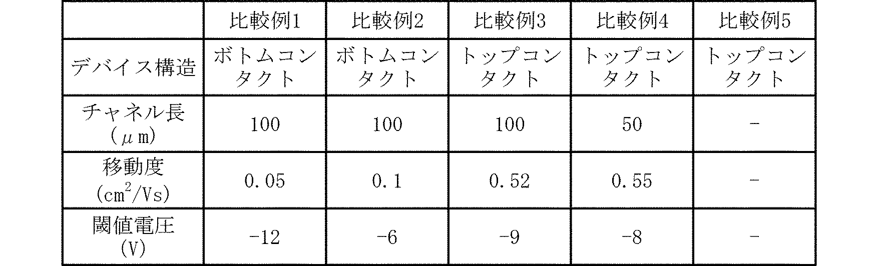
上記結果から明らかなように、実施例1~6の本発明の有機薄膜トランジスタは、従来のボトムコンタクト型の有機薄膜トランジスタ(比較例1~2)に比べて移動度に優れ、トップコンタクト型の有機薄膜トランジスタ(比較例3~4)と同等の移動度及び閾値電圧を有していた。この理由としては、本発明の有機薄膜トランジスタは、ゲート絶縁層の上面に形成した凹溝内にソース電極及びドレイン電極を形成するので、ソース電極とゲート絶縁層との間の段差、及びドレイン電極とゲート絶縁層との間の段差が埋まり、電極端部における結晶性の乱れを抑えることができ、有機半導体層と電極との間の大きな電気的接触抵抗が解決される結果によるものであると推測される。
また、比較例5の結果から明らかなように、トップコンタクト型の有機薄膜トランジスタでは、電極間のチャネル長を10μmに形成することができなかったが、本発明の有機薄膜トランジスタは、チャネル長10μmで電極を形成でき、高精細なパターン形成が可能であった。
1:支持基板
2:ゲート電極
3、3’:ゲート絶縁層
3a:無機酸化物層
3b:高分子絶縁層
4:モールド
4a:凹凸パターン
5a:ソース電極用凹溝
5b:ドレイン電極用凹溝
6:ソース電極
7:ドレイン電極
8:有機半導体層
2:ゲート電極
3、3’:ゲート絶縁層
3a:無機酸化物層
3b:高分子絶縁層
4:モールド
4a:凹凸パターン
5a:ソース電極用凹溝
5b:ドレイン電極用凹溝
6:ソース電極
7:ドレイン電極
8:有機半導体層
Claims (9)
- 支持基板に形成されたゲート電極と、前記ゲート電極上に形成されたゲート絶縁層と、前記ゲート絶縁層上に形成されたソース電極及びドレイン電極と、前記ソース電極及び前記ドレイン電極上に直接又は他の層を介して形成された有機半導体層とを備えた有機薄膜トランジスタであって、
前記ゲート絶縁層の上面に所定パターンの凹溝が形成され、該凹溝内に前記ソース電極及び前記ドレイン電極が形成されていることを特徴とする有機薄膜トランジスタ。 - 前記ゲート絶縁層が、高分子絶縁層で構成される、請求項1に記載の有機薄膜トランジスタ。
- 前記ゲート絶縁層が、無機酸化物層と高分子絶縁層とで構成され、
前記ゲート電極側に前記無機酸化物層が配置され、前記有機半導体層側に前記高分子絶縁層が配置されている、請求項1に記載の有機薄膜トランジスタ。 - 前記ゲート絶縁層と前記有機半導体層との間に自己組織化単分子層が介在している請求項1~3のいずれか1項に記載の有機薄膜トランジスタ。
- 支持基板に形成されたゲート電極上にゲート絶縁層を形成するゲート絶縁層形成工程と、
前記ゲート絶縁層に対し、所望のパターンが形成されたモールドを加熱しながら加圧接触させて、前記ゲート絶縁層の上面に前記モールドのパターン形状を転写して凹溝を形成する凹溝形成工程と、
前記凹溝形成工程で形成した凹溝内に、ソース電極及びドレイン電極を形成するソース・ドレイン電極形成工程と、
前記ソース電極及び前記ドレイン電極上に、直接又は他の層を介して有機半導体層を形成する有機半導体層形成工程とを少なくとも備えることを特徴とする有機薄膜トランジスタの製造方法。 - 前記ゲート絶縁層形成工程において、高分子絶縁材料を用いて前記ゲート絶縁層を形成する、請求項5に記載の有機薄膜トランジスタの製造方法。
- 前記ゲート絶縁層形成工程において、無機酸化物を用いて無機酸化物層を形成した後、該無機酸化物層上に、高分子絶縁材料を用いて高分子絶縁層を形成して、前記ゲート絶縁層を形成する、請求項5に記載の有機薄膜トランジスタの製造方法。
- 前記ソース・ドレイン電極形成工程において、前記ゲート絶縁層上面に形成した前記凹溝内に前記ソース電極と前記ドレイン電極とを形成した後、前記ゲート絶縁層表面を平坦化処理する、請求項4~7のいずれか1項に記載の有機薄膜トランジスタの製造方法。
- 有機半導体層形成工程において、前記ゲート絶縁層上に自己組織化単分子層を形成した後、該自己組織化単分子層上に有機半導体層を形成する、請求項4~8のいずれか1項に記載の有機薄膜トランジスタの製造方法。
Applications Claiming Priority (2)
| Application Number | Priority Date | Filing Date | Title |
|---|---|---|---|
| JP2011-246503 | 2011-11-10 | ||
| JP2011246503 | 2011-11-10 |
Publications (1)
| Publication Number | Publication Date |
|---|---|
| WO2013069366A1 true WO2013069366A1 (ja) | 2013-05-16 |
Family
ID=48289752
Family Applications (1)
| Application Number | Title | Priority Date | Filing Date |
|---|---|---|---|
| PCT/JP2012/072690 Ceased WO2013069366A1 (ja) | 2011-11-10 | 2012-09-06 | 有機薄膜トランジスタ及びその製造方法 |
Country Status (1)
| Country | Link |
|---|---|
| WO (1) | WO2013069366A1 (ja) |
Cited By (2)
| Publication number | Priority date | Publication date | Assignee | Title |
|---|---|---|---|---|
| CN107039534A (zh) * | 2017-05-02 | 2017-08-11 | 中国科学院微电子研究所 | 一种薄膜晶体管及其制备方法 |
| CN114927615A (zh) * | 2022-05-06 | 2022-08-19 | 华南师范大学 | 一种有机场效应晶体管及其制备方法 |
Citations (5)
| Publication number | Priority date | Publication date | Assignee | Title |
|---|---|---|---|---|
| JP2004235298A (ja) * | 2003-01-29 | 2004-08-19 | Pioneer Electronic Corp | 有機半導体素子及びその製造方法 |
| JP2005519486A (ja) * | 2002-03-07 | 2005-06-30 | スリーエム イノベイティブ プロパティズ カンパニー | ゲート絶縁膜の改質した表面を有する有機薄膜トランジスタ |
| JP2006041219A (ja) * | 2004-07-28 | 2006-02-09 | Sony Corp | 半導体装置及びその製造方法 |
| JP2008041914A (ja) * | 2006-08-04 | 2008-02-21 | Chiba Univ | 有機薄膜トランジスタ及びその製造方法。 |
| JP2010141141A (ja) * | 2008-12-11 | 2010-06-24 | Nippon Hoso Kyokai <Nhk> | 薄膜トランジスタおよびその製造方法、並びに表示装置 |
-
2012
- 2012-09-06 WO PCT/JP2012/072690 patent/WO2013069366A1/ja not_active Ceased
Patent Citations (5)
| Publication number | Priority date | Publication date | Assignee | Title |
|---|---|---|---|---|
| JP2005519486A (ja) * | 2002-03-07 | 2005-06-30 | スリーエム イノベイティブ プロパティズ カンパニー | ゲート絶縁膜の改質した表面を有する有機薄膜トランジスタ |
| JP2004235298A (ja) * | 2003-01-29 | 2004-08-19 | Pioneer Electronic Corp | 有機半導体素子及びその製造方法 |
| JP2006041219A (ja) * | 2004-07-28 | 2006-02-09 | Sony Corp | 半導体装置及びその製造方法 |
| JP2008041914A (ja) * | 2006-08-04 | 2008-02-21 | Chiba Univ | 有機薄膜トランジスタ及びその製造方法。 |
| JP2010141141A (ja) * | 2008-12-11 | 2010-06-24 | Nippon Hoso Kyokai <Nhk> | 薄膜トランジスタおよびその製造方法、並びに表示装置 |
Cited By (3)
| Publication number | Priority date | Publication date | Assignee | Title |
|---|---|---|---|---|
| CN107039534A (zh) * | 2017-05-02 | 2017-08-11 | 中国科学院微电子研究所 | 一种薄膜晶体管及其制备方法 |
| CN114927615A (zh) * | 2022-05-06 | 2022-08-19 | 华南师范大学 | 一种有机场效应晶体管及其制备方法 |
| CN114927615B (zh) * | 2022-05-06 | 2026-04-10 | 华南师范大学 | 一种有机场效应晶体管及其制备方法 |
Similar Documents
| Publication | Publication Date | Title |
|---|---|---|
| US7816672B2 (en) | Wiring pattern, electronic device, organic semiconductor device, layered wiring pattern, and layered wiring substrate using the wiring pattern | |
| CN105152125A (zh) | 一种基于微沟道结构的微纳米材料有序自组装图形化方法 | |
| CN101595568B (zh) | 薄膜半导体装置的制作方法及薄膜半导体装置 | |
| TW200843118A (en) | Ambipolar transistor design | |
| TWI514570B (zh) | 場效電晶體,其製造方法及使用其等之電子裝置 | |
| TW201119110A (en) | Fabrication method of organic thin-film transistors | |
| JP6393936B2 (ja) | 薄膜トランジスタ、トランジスタアレイ、薄膜トランジスタの製造方法及びトランジスタアレイの製造方法 | |
| Zhang et al. | High-resolution inkjet-printed oxide thin-film transistors with a self-aligned fine channel bank structure | |
| US20090001362A1 (en) | Organic Thin Film Transistor and Manufacturing Process the Same | |
| WO2013069366A1 (ja) | 有機薄膜トランジスタ及びその製造方法 | |
| KR20130079393A (ko) | 유기 반도체막 및 그 제조 방법, 그리고 콘택트 프린트용 스탬프 | |
| WO2007119442A1 (ja) | 電荷移動度が改善された有機トランジスタ及びその製造方法 | |
| JP5261746B2 (ja) | 有機薄膜トランジスタの製造方法 | |
| Liu et al. | High-performance, all-solution-processed organic nanowire transistor arrays with inkjet-printing patterned electrodes | |
| US20090117686A1 (en) | Method of fabricating organic semiconductor device | |
| JP6393937B2 (ja) | 薄膜トランジスタの製造方法、薄膜トランジスタ及びトランジスタアレイ | |
| JP2011187750A (ja) | 有機薄膜トランジスタの製造方法、有機薄膜トランジスタレイの製造方法及び表示装置の製造方法 | |
| KR20080066152A (ko) | 계면특성이 향상된 유기 반도체층을 갖는 유기박막트랜지스터 및 그 제조 방법 | |
| US9391168B2 (en) | Manufacturing method of a thin film transistor utilizing a pressing mold and active-matrix display devices made therefrom | |
| JP2018037486A (ja) | 薄膜トランジスタの製造方法 | |
| JP6321992B2 (ja) | 電極修飾用組成物、電極修飾方法および有機薄膜トランジスタの製造方法 | |
| JP2007158140A (ja) | 有機トランジスタ | |
| CN102655213A (zh) | 半导体器件结构及其制备方法 | |
| JP2010027869A (ja) | 薄膜トランジスタ及びその製造方法並びに導電性パターン及びその形成方法 | |
| CN105047819B (zh) | 一种有机半导体纳米线阵列导电沟道薄膜晶体管制备方法 |
Legal Events
| Date | Code | Title | Description |
|---|---|---|---|
| 121 | Ep: the epo has been informed by wipo that ep was designated in this application |
Ref document number: 12848514 Country of ref document: EP Kind code of ref document: A1 |
|
| NENP | Non-entry into the national phase |
Ref country code: DE |
|
| 122 | Ep: pct application non-entry in european phase |
Ref document number: 12848514 Country of ref document: EP Kind code of ref document: A1 |
|
| NENP | Non-entry into the national phase |
Ref country code: JP |