WO2013042699A1 - Composé de spirobifluorène, colorant pour transducteur photoélectrique, et transducteur photoélectrique les utilisant - Google Patents
Composé de spirobifluorène, colorant pour transducteur photoélectrique, et transducteur photoélectrique les utilisant Download PDFInfo
- Publication number
- WO2013042699A1 WO2013042699A1 PCT/JP2012/073986 JP2012073986W WO2013042699A1 WO 2013042699 A1 WO2013042699 A1 WO 2013042699A1 JP 2012073986 W JP2012073986 W JP 2012073986W WO 2013042699 A1 WO2013042699 A1 WO 2013042699A1
- Authority
- WO
- WIPO (PCT)
- Prior art keywords
- group
- photoelectric conversion
- conversion element
- dye
- semiconductor
- Prior art date
Links
Images

Classifications
-
- C—CHEMISTRY; METALLURGY
- C07—ORGANIC CHEMISTRY
- C07D—HETEROCYCLIC COMPOUNDS
- C07D333/00—Heterocyclic compounds containing five-membered rings having one sulfur atom as the only ring hetero atom
- C07D333/02—Heterocyclic compounds containing five-membered rings having one sulfur atom as the only ring hetero atom not condensed with other rings
- C07D333/04—Heterocyclic compounds containing five-membered rings having one sulfur atom as the only ring hetero atom not condensed with other rings not substituted on the ring sulphur atom
- C07D333/06—Heterocyclic compounds containing five-membered rings having one sulfur atom as the only ring hetero atom not condensed with other rings not substituted on the ring sulphur atom with only hydrogen atoms, hydrocarbon or substituted hydrocarbon radicals, directly attached to the ring carbon atoms
- C07D333/24—Radicals substituted by carbon atoms having three bonds to hetero atoms with at the most one bond to halogen, e.g. ester or nitrile radicals
-
- C—CHEMISTRY; METALLURGY
- C07—ORGANIC CHEMISTRY
- C07D—HETEROCYCLIC COMPOUNDS
- C07D495/00—Heterocyclic compounds containing in the condensed system at least one hetero ring having sulfur atoms as the only ring hetero atoms
- C07D495/02—Heterocyclic compounds containing in the condensed system at least one hetero ring having sulfur atoms as the only ring hetero atoms in which the condensed system contains two hetero rings
- C07D495/04—Ortho-condensed systems
-
- C—CHEMISTRY; METALLURGY
- C07—ORGANIC CHEMISTRY
- C07D—HETEROCYCLIC COMPOUNDS
- C07D519/00—Heterocyclic compounds containing more than one system of two or more relevant hetero rings condensed among themselves or condensed with a common carbocyclic ring system not provided for in groups C07D453/00 or C07D455/00
-
- C—CHEMISTRY; METALLURGY
- C09—DYES; PAINTS; POLISHES; NATURAL RESINS; ADHESIVES; COMPOSITIONS NOT OTHERWISE PROVIDED FOR; APPLICATIONS OF MATERIALS NOT OTHERWISE PROVIDED FOR
- C09B—ORGANIC DYES OR CLOSELY-RELATED COMPOUNDS FOR PRODUCING DYES, e.g. PIGMENTS; MORDANTS; LAKES
- C09B23/00—Methine or polymethine dyes, e.g. cyanine dyes
- C09B23/0008—Methine or polymethine dyes, e.g. cyanine dyes substituted on the polymethine chain
- C09B23/005—Methine or polymethine dyes, e.g. cyanine dyes substituted on the polymethine chain the substituent being a COOH and/or a functional derivative thereof
- C09B23/0058—Methine or polymethine dyes, e.g. cyanine dyes substituted on the polymethine chain the substituent being a COOH and/or a functional derivative thereof the substituent being CN
-
- C—CHEMISTRY; METALLURGY
- C09—DYES; PAINTS; POLISHES; NATURAL RESINS; ADHESIVES; COMPOSITIONS NOT OTHERWISE PROVIDED FOR; APPLICATIONS OF MATERIALS NOT OTHERWISE PROVIDED FOR
- C09B—ORGANIC DYES OR CLOSELY-RELATED COMPOUNDS FOR PRODUCING DYES, e.g. PIGMENTS; MORDANTS; LAKES
- C09B23/00—Methine or polymethine dyes, e.g. cyanine dyes
- C09B23/10—The polymethine chain containing an even number of >CH- groups
- C09B23/105—The polymethine chain containing an even number of >CH- groups two >CH- groups
-
- C—CHEMISTRY; METALLURGY
- C09—DYES; PAINTS; POLISHES; NATURAL RESINS; ADHESIVES; COMPOSITIONS NOT OTHERWISE PROVIDED FOR; APPLICATIONS OF MATERIALS NOT OTHERWISE PROVIDED FOR
- C09B—ORGANIC DYES OR CLOSELY-RELATED COMPOUNDS FOR PRODUCING DYES, e.g. PIGMENTS; MORDANTS; LAKES
- C09B23/00—Methine or polymethine dyes, e.g. cyanine dyes
- C09B23/10—The polymethine chain containing an even number of >CH- groups
- C09B23/107—The polymethine chain containing an even number of >CH- groups four >CH- groups
-
- C—CHEMISTRY; METALLURGY
- C09—DYES; PAINTS; POLISHES; NATURAL RESINS; ADHESIVES; COMPOSITIONS NOT OTHERWISE PROVIDED FOR; APPLICATIONS OF MATERIALS NOT OTHERWISE PROVIDED FOR
- C09B—ORGANIC DYES OR CLOSELY-RELATED COMPOUNDS FOR PRODUCING DYES, e.g. PIGMENTS; MORDANTS; LAKES
- C09B57/00—Other synthetic dyes of known constitution
-
- C—CHEMISTRY; METALLURGY
- C09—DYES; PAINTS; POLISHES; NATURAL RESINS; ADHESIVES; COMPOSITIONS NOT OTHERWISE PROVIDED FOR; APPLICATIONS OF MATERIALS NOT OTHERWISE PROVIDED FOR
- C09B—ORGANIC DYES OR CLOSELY-RELATED COMPOUNDS FOR PRODUCING DYES, e.g. PIGMENTS; MORDANTS; LAKES
- C09B69/00—Dyes not provided for by a single group of this subclass
- C09B69/008—Dyes containing a substituent, which contains a silicium atom
-
- H—ELECTRICITY
- H10—SEMICONDUCTOR DEVICES; ELECTRIC SOLID-STATE DEVICES NOT OTHERWISE PROVIDED FOR
- H10K—ORGANIC ELECTRIC SOLID-STATE DEVICES
- H10K85/00—Organic materials used in the body or electrodes of devices covered by this subclass
- H10K85/60—Organic compounds having low molecular weight
- H10K85/615—Polycyclic condensed aromatic hydrocarbons, e.g. anthracene
- H10K85/626—Polycyclic condensed aromatic hydrocarbons, e.g. anthracene containing more than one polycyclic condensed aromatic rings, e.g. bis-anthracene
-
- H—ELECTRICITY
- H10—SEMICONDUCTOR DEVICES; ELECTRIC SOLID-STATE DEVICES NOT OTHERWISE PROVIDED FOR
- H10K—ORGANIC ELECTRIC SOLID-STATE DEVICES
- H10K85/00—Organic materials used in the body or electrodes of devices covered by this subclass
- H10K85/60—Organic compounds having low molecular weight
- H10K85/649—Aromatic compounds comprising a hetero atom
- H10K85/655—Aromatic compounds comprising a hetero atom comprising only sulfur as heteroatom
-
- H—ELECTRICITY
- H01—ELECTRIC ELEMENTS
- H01G—CAPACITORS; CAPACITORS, RECTIFIERS, DETECTORS, SWITCHING DEVICES OR LIGHT-SENSITIVE DEVICES, OF THE ELECTROLYTIC TYPE
- H01G9/00—Electrolytic capacitors, rectifiers, detectors, switching devices, light-sensitive or temperature-sensitive devices; Processes of their manufacture
- H01G9/20—Light-sensitive devices
- H01G9/2027—Light-sensitive devices comprising an oxide semiconductor electrode
- H01G9/2031—Light-sensitive devices comprising an oxide semiconductor electrode comprising titanium oxide, e.g. TiO2
-
- H—ELECTRICITY
- H01—ELECTRIC ELEMENTS
- H01G—CAPACITORS; CAPACITORS, RECTIFIERS, DETECTORS, SWITCHING DEVICES OR LIGHT-SENSITIVE DEVICES, OF THE ELECTROLYTIC TYPE
- H01G9/00—Electrolytic capacitors, rectifiers, detectors, switching devices, light-sensitive or temperature-sensitive devices; Processes of their manufacture
- H01G9/20—Light-sensitive devices
- H01G9/2059—Light-sensitive devices comprising an organic dye as the active light absorbing material, e.g. adsorbed on an electrode or dissolved in solution
Definitions
- the present invention relates to a spirobifluorene compound, a dye for a photoelectric conversion element, a semiconductor electrode for a photoelectric conversion element using the same, a photoelectric conversion element, and a photoelectrochemical cell.
- Solar cells that convert light energy into electrical energy include inorganic solar cells that use inorganic materials such as single crystal silicon, polycrystalline silicon, and amorphous silicon, and organic solar cells that use organic dyes and conductive polymer materials. Solar cells have been proposed.
- a Gretzel type solar cell includes a semiconductor electrode in which a semiconductor layer having a dye adsorbed thereon is formed on a conductive substrate, a counter electrode made of a conductive substrate opposite to the electrode, and an electrolyte layer held between the electrodes. And.
- the adsorbed dye absorbs light and enters an excited state, and electrons are injected from the excited dye into the semiconductor layer.
- the dye that is in an oxidized state due to the emission of electrons returns to the original dye by transferring electrons to the dye by the oxidation reaction of the redox agent in the electrolyte layer. Then, the redox agent that has donated electrons to the dye is reduced again on the counter electrode side. This series of reactions functions as a battery.
- the effective reaction surface area increased about 1000 times by using porous titanium oxide in which fine particles were sintered in the semiconductor layer, and a photocurrent larger than the conventional one could be taken out. It is a big feature.
- a metal complex such as a ruthenium complex is used as a sensitizing dye.
- a metal complex such as a ruthenium complex
- a metal complex such as a ruthenium complex
- a metal complex such as a ruthenium complex
- cis-bis (isothiocyanato) -bis- (2,2′-bipyridyl-4,4′-dicarboxylic acid) ruthenium (II) etc.
- organic dyes that do not contain noble metals such as ruthenium is required as sensitizing dyes in dye-sensitized solar cells.
- organic dyes have a higher molar extinction coefficient than metal complexes such as ruthenium complexes, and further have a high degree of freedom in molecular design, so that development of dyes with high photoelectric conversion efficiency is expected.
- the present invention has been made in order to solve the above problems, and provides a dye for a photoelectric conversion element having excellent photoelectric conversion characteristics, a semiconductor electrode for a photoelectric conversion element, a photoelectric conversion element and a photoelectrochemical cell using the same. It is to provide.
- spirobifluorene compounds can be dyes for photoelectric conversion elements having excellent photoelectric conversion characteristics.
- the compound of the present invention is a spirobifluorene compound represented by the following general formula (1), a tautomer or a stereoisomer thereof.
- R 1 and R 2 each independently represent a hydrogen atom, a substituted or unsubstituted alkyl group, an alkoxy group, or a hydroxy group.
- Z represents a ⁇ -conjugated linking group.
- X represents an organic group having an acidic group.
- the dye for a photoelectric conversion device of the present invention includes at least one of the spirobifluorene-based compound of the present invention, a tautomer or a stereoisomer thereof.
- the semiconductor electrode for photoelectric conversion elements of the present invention has a semiconductor layer containing the dye for photoelectric conversion elements of the present invention.
- the photoelectric conversion element of the present invention has the semiconductor electrode for a photoelectric conversion element of the present invention.
- the photoelectrochemical cell of the present invention has the photoelectric conversion element of the present invention.
- a spirobifluorene compound having excellent photoelectric conversion characteristics can be provided.
- the compound can provide a dye for a photoelectric conversion element having excellent photoelectric conversion characteristics, a semiconductor electrode for a photoelectric conversion element using the same, a photoelectric conversion element, and a photoelectrochemical cell.
- a spirobifluorene compound suitable for the photoelectric conversion dye according to the present embodiment is a compound represented by the following general formula (1).
- the spirobifluorene compound of the present invention has isomers such as tautomers or stereoisomers (eg, geometric isomers, conformers and optical isomers), any isomers It can be used in the present invention.
- R 1 and R 2 in the general formula (1) each independently represent a hydrogen atom, a substituted or unsubstituted alkyl group, an alkoxy group, or a hydroxy group.
- the substituted or unsubstituted alkyl group include methyl group, ethyl group, propyl group, iso-propyl group, n-butyl group, t-butyl group, pentyl group, neo-pentyl group, cyclopentyl group, hexyl group and cyclohexyl group.
- a linear, branched or cyclic alkyl group having 1 to 8 carbon atoms such as a heptyl group and an octyl group, an aralkyl group such as a benzyl group in which the alkyl group is substituted with a phenyl group, and the like, and a hydroxy group substituted on the alkyl group
- Examples thereof include a hydroxyalkyl group and an alkoxyalkyl group obtained by substituting an alkoxy group (for example, an alkoxy group having 1 to 4 carbon atoms) with these alkyl groups.
- Examples of the substituted or unsubstituted alkoxy group include a methoxy group, an ethoxy group, a propoxy group, an iso-propoxy group, an n-butoxy group, a t-butoxy group, an n-hexyloxy group, a cyclohexyloxy group, and an n-octyloxy group.
- Z represents a ⁇ -conjugated linking group, specifically, a substituted or unsubstituted aromatic ring, a substituted or unsubstituted heterocyclic ring, a vinylene group (—CH ⁇ CH—), an ethynylene group (—C ⁇ C— ) Represents a linking group containing at least one selected from the group consisting of
- the linking group Z is not particularly limited, but is preferably an atomic group that can be conjugated with the spirobifluorene ring to which Z is bonded and the organic group X having an acidic group.
- the linking group Z is preferably a linking group having a structure represented by at least the following general formula (2).
- R 3 and R 4 each independently represent a hydrogen atom, a substituted or unsubstituted alkyl group, or a substituted or unsubstituted alkoxy group, and R 3 and R 4 are connected to each other.
- a ring may be formed.
- the substituted or unsubstituted alkyl group include a methyl group, an ethyl group, a propyl group, an iso-propyl group, an n-butyl group, a t-butyl group, a pentyl group, a neo-pentyl group, a hexyl group, a heptyl group, and an octyl group.
- Examples of the substituent bonded to the alkyl group include a hydroxy group and an alkoxy group.
- Examples of the substituted or unsubstituted alkoxy group include linear or branched alkoxy groups having 1 to 4 carbon atoms such as a methoxy group, an ethoxy group, a propoxy group, an iso-propoxy group, a butoxy group, and a t-butoxy group.
- examples of the ring formed by connecting R 3 and R 4 include a cycloheptane ring, a cyclohexane ring, a tetrahydrofuran ring, a tetrahydropyran ring, a dioxane ring, and a dioxepane ring. These rings may have a substituent which the alkyl group and alkoxy group may have.
- Y represents an oxygen atom, a sulfur atom or NRa
- Ra represents a hydrogen atom, a substituted or unsubstituted alkyl group, or a substituted or unsubstituted aryl group.
- the substituted or unsubstituted alkyl group include the same alkyl groups as the substituted or unsubstituted alkyl groups of R 1 and R 2 described above.
- the unsubstituted aryl group include a phenyl group and a naphthyl group.
- the substituent bonded to the aryl group include an alkyl group, a hydroxy group, an alkoxy group, and an N, N-dialkylamino group.
- substituted aryl group examples include a tolyl group, 4-t-butylphenyl group, 3,5-di-t-butylphenyl group, 4-methoxyphenyl group, 4- (N, N-dimethylamino) phenyl group and the like. It is done. * Indicates a bond.
- two structures represented by the general formula (2) may be linked, and the substituents may be bonded to each other to form a tricyclic linking group. It may be another bonding part such as a (or diaryl) silyl group.
- a structure in which two or more 5-membered ring structures of the general formula (2) are condensed for example, a thienofuran, a thienothiophene, a thienopyrrole structure, or the like may be used.
- linking group Z are shown in the chemical formulas (Z1) to (Z29), but are not limited thereto.
- carbons constituting the rings are directly bonded to each other or bonded by forming a condensed ring.
- a group in which a plurality of these linking groups are linked may be used.
- the spirobifluorene ring is shown as being bonded to the left bond and the organic group X having an acidic group is bonded to the right bond, but it may be in the opposite direction.
- X in the formula (1) represents an organic group having an acidic group.
- the acidic group of the organic group X include a carboxy group, a sulfonic acid group, a phosphonic acid group, or a salt thereof, and among them, a carboxy group or a salt thereof is particularly preferable.
- at least one acidic group may be included, but a plurality of acidic groups may be included.
- the acidic group is a salt, a monovalent or divalent metal salt, ammonium salt or organic ammonium salt is preferred.
- the monovalent or divalent metal salt include alkali metal salts such as Li, Na, K, and Cs, and alkaline earth metal salts such as Mg, Ca, and Sr.
- the organic group of the organic ammonium salt include an alkyl group having 1 to 8 carbon atoms, an alkenyl group having 1 to 8 carbon atoms, and an aryl group having 6 to 12 carbon atoms.
- the spirobifluorene compound represented by the general formula (1) preferably has a functional group that can be adsorbed to the semiconductor layer from the viewpoint of adsorbing to the semiconductor layer used in the semiconductor electrode, and the acidic group of the organic group X is a functional group. Can play the role of a group.
- Specific examples of the organic group X having an acidic group are shown by chemical formulas (X1) to (X16) in Tables 3 and 4, but are not limited thereto. These organic groups X have a carbon-carbon double bond in addition to the acidic group, and one bond of the linking group Z is bonded to one carbon of the carbon-carbon double bond, and the other carbon. A cyano group, a carbonyl group, or another carbon-carbon double bond carbon is bonded to.
- the organic group X having an acidic group is preferably a group represented by the following general formula (3).
- M represents a hydrogen atom or a salt-forming cation.
- Examples of the salt-forming cation include various cations capable of forming a salt with a carboxy group.
- Examples of such a cation include an ammonium cation (NH 4 + ); an organic ammonium cation derived from an amine (A 1 A 2 A 3 A 4 N + , and A 1 to A 4 are a hydrogen atom or an organic group. shown, but at least one of which is an organic group); Li +, Na +, K +, alkali metal ions Cs +, etc.; 1 / 2Mg 2+, 1 / 2Ca 2+, 1 / 2Sr alkaline earth metals such as 2+ A metal ion etc. are mentioned.
- Examples of the organic group represented by A 1 to A 4 of the organic ammonium cation include an alkyl group having 1 to 8 carbon atoms, an alkenyl group having 1 to 8 carbon atoms, and an aryl group having 6 to 12 carbon atoms.
- Examples of the combination of Z and X in the spirobifluorene compound represented by the general formula (1), the tautomer or stereoisomer thereof include, for example, a-1 to a-29, b-1 to b-29, c-1 to c-29, d-1 to d-13, e-1 to e-13, f-1 to f-13, g-1 to g- 13, h-1 to h-13, and i-1 to i-13, but are not limited thereto.
- the compounds of the present invention are, for example, spirobifluorene compounds such as compounds SP-1 to SP-12 shown in Table 8 and Table 9 below, tautomers or stereoisomers thereof, or salts thereof. Particularly preferred.
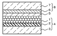
- FIG. 1 schematically shows a cross-sectional structure of an example of the photoelectric conversion element according to the present embodiment.
- the photoelectric conversion element shown in FIG. 1 includes a semiconductor electrode 4, a counter electrode 8, and an electrolyte layer (charge transport layer) 5 held between both electrodes.
- the semiconductor electrode 4 includes a conductive substrate including the light transmissive substrate 3 and the transparent conductive layer 2, and the semiconductor layer 1.
- the counter electrode 8 includes a catalyst layer 6 and a substrate 7.
- the semiconductor layer 1 is adsorbed with a spirobifluorene compound according to the present invention, a dye containing at least one of its tautomers or stereoisomers.
- the dye adsorbed on the semiconductor layer 1 is excited and emits electrons.
- the electrons move to the conduction band of the semiconductor, and further move to the transparent conductive layer 2 by diffusion.
- the electrons in the transparent conductive layer 2 move to the counter electrode 8 via an external circuit (not shown).
- dye which emitted the electron receives an electron from the electrolyte layer 5 (reduced), returns to the original state, and a pigment
- the electrons moved to the counter electrode are given to the electrolyte layer 5 and the electrolyte is reduced. In this manner, the photoelectric conversion element functions as a battery.
- each component will be described by taking the photoelectric conversion element shown in FIG. 1 as an example.
- the semiconductor electrode 4 includes a conductive substrate including the light transmissive substrate 3 and the transparent conductive layer 2, and the semiconductor layer 1. As shown in FIG. 1, a light transmissive substrate 3, a transparent conductive layer 2, and a semiconductor layer 1 are laminated in this order from the outside to the inside of the element. A dye (not shown) is adsorbed on the semiconductor layer 1.
- the conductive substrate of the semiconductor electrode 4 may have a single layer structure in which the substrate itself has conductivity, or a two-layer structure in which a conductive layer is formed on the substrate.
- the conductive substrate of the photoelectric conversion element shown in FIG. 1 has a two-layer structure in which a transparent conductive layer 2 is formed on a light transmissive substrate 3.
- the substrate used for the conductive substrate examples include a glass substrate, a plastic substrate, and a metal plate.
- a substrate having high light transmittance such as a transparent glass substrate and a plastic substrate
- the material for the transparent plastic substrate include polyethylene terephthalate (PET), polyethylene naphthalate (PEN), polycarbonate (PC), polycycloolefin, polyphenylene sulfide, and the like.
- PET polyethylene terephthalate
- PEN polyethylene naphthalate
- PC polycarbonate
- polycycloolefin polyphenylene sulfide
- the semiconductor layer is formed by sintering as described later, it is preferable to use a glass substrate having excellent heat resistance.
- the conductive layer (for example, the transparent conductive layer 2) formed on the substrate (for example, the light transmissive substrate 3) is not particularly limited, but for example, indium tin oxide (Indium-Tin-Oxide: ITO), A transparent conductive layer made of a transparent material such as fluorine-doped tin oxide (FTO), indium-zinc oxide (IZO), tin oxide (SnO 2 ), or the like is preferable.
- the conductive layer formed over the substrate can be formed into a film shape over the entire surface or a part of the surface of the substrate.
- the thickness of the conductive layer can be selected as appropriate, but is preferably about 0.02 ⁇ m or more and 10 ⁇ m or less. Such a conductive layer can be formed using a normal film formation technique.
- the conductive substrate in this embodiment can also use a metal lead wire for the purpose of reducing the resistance of the conductive substrate.
- the metal lead wire include metals such as aluminum, copper, gold, silver, platinum, and nickel.
- the metal lead wire can be produced by vapor deposition, sputtering, or the like.
- a conductive layer for example, transparent conductive layer 2 such as ITO or FTO
- a metal lead wire may be formed on the conductive layer.
- the following description of the present embodiment is based on an example in which a conductive substrate having a two-layer structure in which the transparent conductive layer 2 is formed on the light-transmitting substrate 3 is used as the conductive substrate of the semiconductor electrode. It is not limited to examples.
- a semiconductor layer As a material constituting the semiconductor layer 1, a single semiconductor such as silicon or germanium, a compound semiconductor such as a metal chalcogenide, a compound having a perovskite structure, or the like can be used.
- Metal chalcogenides include oxides such as titanium, tin, zinc, iron, tungsten, indium, zirconium, vanadium, niobium, tantalum, strontium, hafnium, cerium, lanthanum; cadmium, zinc, lead, silver, antimony, bismuth, etc. Sulfides; selenides such as cadmium and lead; tellurides of cadmium and the like.
- Examples of other compound semiconductors include phosphides such as zinc, gallium, indium, and cadmium; gallium arsenide; copper-indium-selenide; copper-indium-sulfide, and the like.
- Examples of the compound having a perovskite structure include commonly known semiconductor compounds such as barium titanate, strontium titanate, and potassium niobate. These semiconductor materials can be used alone or in combination of two or more.
- a semiconductor material containing titanium oxide or zinc oxide is preferable, and a semiconductor material containing titanium oxide is more preferable.
- titanium oxide include various types of titanium oxide such as anatase type titanium oxide, rutile type titanium oxide, amorphous titanium oxide, metatitanic acid, orthotitanic acid, and a titanium oxide-containing complex can be used. .
- anatase type titanium oxide is preferable from the viewpoint of further improving the stability of photoelectric conversion.
- Examples of the form of the semiconductor layer include a porous semiconductor layer obtained by sintering semiconductor fine particles, a thin film semiconductor layer obtained by a sol-gel method, a sputtering method, a spray pyrolysis method, and the like. Moreover, it is good also as a semiconductor layer which consists of a fibrous semiconductor layer or an acicular crystal
- the form of these semiconductor layers can be appropriately selected according to the purpose of use of the photoelectric conversion element. Among these, a semiconductor layer having a large specific surface area such as a porous semiconductor layer and a needle-like semiconductor layer is preferable from the viewpoint of the amount of dye adsorbed.
- a porous semiconductor layer formed from semiconductor fine particles is preferable from the viewpoint that the utilization factor of incident light and the like can be adjusted by the particle size of the semiconductor fine particles.
- the semiconductor layer may be a single layer or a multilayer. By forming a multilayer, a sufficiently thick semiconductor layer can be more easily formed.
- the porous semiconductor layer formed from semiconductor fine particles is a multilayer, it may consist of a plurality of semiconductor layers having different average particle diameters of the semiconductor fine particles. For example, the average particle diameter of the semiconductor fine particles of the semiconductor layer closer to the light incident side (first semiconductor layer) may be smaller than that of the semiconductor layer farther from the light incident side (second semiconductor layer).
- the first semiconductor layer absorbs a lot of light, and the light that has passed through the first semiconductor layer is efficiently scattered by the second semiconductor layer and returned to the first semiconductor layer, and the returned light is returned to the first semiconductor layer.
- the whole optical absorptance can be improved further.
- the film thickness of the semiconductor layer is not particularly limited, but can be set to, for example, not less than 0.5 ⁇ m and not more than 45 ⁇ m from the viewpoints of permeability and conversion efficiency.
- the specific surface area of the semiconductor layer can be set to, for example, 10 m 2 / g or more and 200 m 2 / g or less from the viewpoint of adsorbing a large amount of dye.
- the porosity of the porous semiconductor layer is, for example, 40% or more and 80 from the viewpoint that ions in the electrolyte are further sufficiently diffused and charge transport is performed. % Or less is preferable.
- the porosity is a percentage of the volume of the semiconductor layer occupied by the pores in the semiconductor layer.
- the porous semiconductor layer can be formed, for example, as follows.
- a suspension is prepared by adding semiconductor fine particles together with an organic compound such as a resin and a dispersant to a dispersion medium such as an organic solvent and water. And this suspension is apply
- an organic compound is added to the dispersion medium together with the semiconductor fine particles, the organic compound burns during firing, and it becomes possible to secure a further sufficient gap (void) in the porous semiconductor layer.
- the porosity can be changed by controlling the molecular weight and the addition amount of the organic compound combusted during firing.
- the organic compound to be used is not particularly limited as long as it can be dissolved in a suspension and burned and removed during firing.
- polyethylene glycol, cellulose ester resin, cellulose ether resin, epoxy resin, urethane resin, phenol resin, polycarbonate resin, polyarylate resin, polyvinyl butyral resin, polyester resin, polyvinyl formal resin, silicon resin, styrene examples thereof include polymers and copolymers of vinyl compounds such as vinyl acetate, acrylic acid esters, and methacrylic acid esters.
- the type and amount of the organic compound can be appropriately selected according to the type and state of the fine particles used, the composition ratio of the suspension, the total weight, and the like.
- the ratio of the semiconductor fine particles is 10% by mass or more with respect to the total weight of the whole suspension, the strength of the prepared film can be further sufficiently increased, and the ratio of the semiconductor fine particles is If the total weight is 40% by mass or less, a porous semiconductor layer having a large porosity can be obtained more stably. Therefore, the ratio of the semiconductor fine particles is based on the total weight of the entire suspension. It is preferable that it is 10 mass% or more and 40 mass% or less.
- semiconductor fine particles single or plural compound semiconductor particles having an appropriate average particle diameter, for example, an average particle diameter of about 1 nm to 500 nm can be used. Among these, from the viewpoint of increasing the specific surface area, those having an average particle diameter of about 1 nm to 50 nm are desirable. In order to increase the utilization factor of incident light, semiconductor particles having a relatively large average particle diameter of about 200 nm to 400 nm may be added.
- Examples of the method for producing semiconductor fine particles include a sol-gel method such as a hydrothermal synthesis method, a sulfuric acid method, and a chlorine method.
- the method is not limited as long as the method can produce the desired fine particles, but from the viewpoint of crystallinity. Is preferably synthesized by a hydrothermal synthesis method.
- dispersion medium for the suspension examples include glyme solvents such as ethylene glycol monomethyl ether; alcohols such as isopropyl alcohol; mixed solvents such as isopropyl alcohol / toluene; water and the like.
- the suspension can be applied by a usual application method such as a doctor blade method, a squeegee method, a spin coating method, or a screen printing method.
- the conditions for drying and baking the coating film after application of the suspension can be, for example, about 10 seconds to 12 hours in the range of about 50 ° C. to 800 ° C. in the air or in an inert gas atmosphere. . This drying and baking can be performed once at a single temperature or twice or more at different temperatures.
- semiconductor layers other than the porous semiconductor layer can be formed using a normal method for forming a semiconductor layer used in a photoelectric conversion element.
- ⁇ Dye> As the dye in the photoelectric conversion device according to the present embodiment, at least one of the above-described spirobifluorene compounds represented by the general formula (1), tautomers or stereoisomers thereof is used. Two or more kinds may be used in combination. Furthermore, other organic pigments can be combined.
- adsorbing the dye to the semiconductor layer for example, a method in which a semiconductor substrate (that is, a conductive substrate having the semiconductor layer 1) is immersed in a solution in which the dye is dissolved, or a dye solution is applied to the semiconductor layer.
- a semiconductor substrate that is, a conductive substrate having the semiconductor layer 1
- a dye solution is applied to the semiconductor layer.
- Solvents for this dye solution include nitrile solvents such as acetonitrile, propionitrile, methoxyacetonitrile; alcohol solvents such as methanol, ethanol, isopropyl alcohol; ketone solvents such as acetone, methyl ethyl ketone, methyl isobutyl ketone, cyclohexanone; acetic acid Ester solvents such as ethyl and butyl acetate; ether solvents such as tetrahydrofuran and dioxane; amide solvents such as N, N-dimethylformamide, N, N-dimethylacetamide and N-methyl-2-pyrrolidone; dichloromethane, chloroform, And halogen solvents such as dichloroethane, trichloroethane, and chlorobenzene; hydrocarbon solvents such as toluene, xylene, and cyclohexane; and water. These may be used alone
- the solution can be stirred, heated to reflux, or ultrasonic waves can be applied.
- the amount of the dye supported can be set in the range of 1 ⁇ 10 ⁇ 10 mol / cm 2 or more and 1 ⁇ 10 ⁇ 4 mol / cm 2 or less, and 1 ⁇ 10 ⁇ 9 mol / cm 2 or more and 9.0 ⁇ 10 ⁇ 6.
- a range of less than mol / cm 2 is preferred. Within this range, the effect of improving the photoelectric conversion efficiency can be obtained economically and sufficiently.
- two or more types of dyes may be mixed and used. It is preferable to select the type and ratio as appropriate.
- an additive may be used in combination when adsorbing the dye in order to suppress a decrease in conversion efficiency due to the association between the dyes.
- additives include steroidal compounds having a carboxy group (for example, deoxycholic acid, cholic acid, chenodeoxycholic acid, etc.).
- the counter electrode 8 in the photoelectric conversion element according to the present embodiment has the catalyst layer 6 on the substrate 7.
- the counter electrode 8 efficiently annihilates electrons and holes.
- the material There is no limit to the material as long as it can fulfill its function.
- the catalyst layer 6 of the counter electrode 8 can be formed as a metal vapor deposition film on the substrate 7 by vapor deposition or the like.
- a Pt layer formed on the substrate 7 may be used.
- the catalyst layer 6 of the counter electrode 8 may contain a nanocarbon material.
- the catalyst layer 6 of the counter electrode 8 may be formed by sintering a paste containing carbon nanotubes, carbon nanohorns, or carbon fibers on the porous insulating film. Nanocarbon materials have a large specific surface area and can improve the probability of annihilation of electrons and holes.
- the substrate 7 examples include transparent substrates such as glass and polymer films, and metal plates (foil).
- a glass with a transparent conductive film is selected as the substrate 7, and platinum, carbon, or the like is formed as the catalyst layer 6 using a vapor deposition method or a sputtering method. be able to.
- the electrolyte layer 5 in the photoelectric conversion element according to the present embodiment has a function of transporting holes generated from the dye adsorbed on the semiconductor layer 1 due to incidence of light to the counter electrode 8.
- an electrolyte layer an electrolyte solution in which a redox couple is dissolved in an organic solvent, a gel electrolyte in which a polymer matrix is impregnated with a liquid in which the redox couple is dissolved in an organic solvent, a molten salt containing the redox couple, a solid electrolyte Organic hole transport materials and the like can be used.
- the electrolyte layer can be composed of an electrolyte, a solvent, and an additive.
- the electrolyte LiI, NaI, KI, CsI , CaI 2 , etc. of the metal iodides, tetraalkylammonium iodide, pyridinium iodide, imidazolium iodide iodide and I 2, such as iodine salts of quaternary ammonium compounds such as id
- a bromide such as a bromide of a quaternary ammonium compound such as a metal bromide such as LiBr, NaBr, KBr, CsBr or CaBr 2 or a tetraalkylammonium bromide or pyridinium bromide with Br 2 ;
- Metal complexes such as ferricyanate and ferrocene-ferricinium ions; sulfur compounds such as sodium polysulfide and alky
- a combination of LiI and pyridinium iodide, or a combination of imidazolium iodide and I 2 is preferable.
- said electrolyte may be used independently or may be used in mixture of 2 or more types.
- a molten salt that is in a molten state at room temperature can be used as the electrolyte. In this case, a solvent need not be used.
- Examples of the solvent used in the electrolyte layer include carbonate solvents such as ethylene carbonate, diethyl carbonate, dimethyl carbonate, and propylene carbonate; amide solvents such as N-methyl-2-pyrrolidone and N, N-dimethylformamide; Nitrile solvents such as propionitrile, propionitrile, methoxyacetonitrile, acetonitrile; lactone solvents such as ⁇ -butyrolactone and valerolactone; ether solvents such as tetrahydrofuran, dioxane, diethyl ether, ethylene glycol dialkyl ether; methanol, ethanol Alcohol solvents such as isopropyl alcohol; aprotic polar solvents such as dimethyl sulfoxide and sulfolane; 2-methyl-3-oxazolidinone, 2-methyl Heterocyclic compounds such as 1,3-dioxolane. These solvents may be used alone or in combination of two or more.
- a basic compound may be added to the electrolyte layer in order to suppress dark current.
- the type of basic compound is not particularly limited, and examples thereof include t-butylpyridine, 2-picoline, 2,6-lutidine and the like.
- the addition concentration in the case of adding a basic compound can be, for example, about 0.05 mol / L or more and 2 mol / L or less.
- a solid electrolyte can also be used.
- a gel electrolyte or a completely solid electrolyte can be used.
- a gelling agent to which an electrolyte or a room temperature molten salt is added can be used.
- gelation can be performed by a technique such as addition of a polymer or an oil gelling agent, polymerization of coexisting polyfunctional monomers, or a crosslinking reaction of the polymer.
- Examples of the polymer to be gelated by adding a polymer include polyacrylonitrile and polyvinylidene fluoride.
- oil gelling agents dibenzylden-D-sorbitol, cholesterol derivatives, amino acid derivatives, alkylamide derivatives of trans- (1R, 2R) -1,2-cyclohexanediamine, alkylurea derivatives, N-octyl-D-gluconamide benzoate Double-headed amino acid derivatives, quaternary ammonium salt derivatives, and the like.
- the monomer used is preferably a compound having two or more ethylenically unsaturated groups, such as divinylbenzene, ethylene glycol dimethacrylate, ethylene glycol diacrylate, Examples include diethylene glycol dimethacrylate, diethylene glycol diacrylate, triethylene glycol dimethacrylate, triethylene glycol diacrylate, pentaerythritol triacrylate, and trimethylolpropane triacrylate.
- a monofunctional monomer may be included in addition to the polyfunctional monomer.
- Monofunctional monomers include esters derived from acrylic acid and ⁇ -alkyl acrylic acids such as acrylamide, N-isopropylacrylamide, methyl acrylate, and hydroxyethyl acrylate; amides; dimethyl maleate, diethyl fumarate, dibutyl maleate Esters derived from maleic acid and fumaric acid such as: Dienes such as butadiene, isoprene and cyclopentadiene; Aromatic vinyl compounds such as styrene, p-chlorostyrene and sodium styrenesulfonate; Vinyl esters such as vinyl acetate Nitriles such as acrylonitrile and methacrylonitrile; vinyl compounds having a nitrogen-containing heterocycle such as vinyl carbazole; vinyl compounds having a quaternary ammonium salt; other N-vinylformamide, vinyl sulfone , Vinylidene fluoride, vinyl alkyl ethers, N- phenylmaleimide, and the
- Polymerization of the monomer for gelation can be performed by radical polymerization.
- This radical polymerization can be carried out by heating, light, ultraviolet light or electron beam, or electrochemically.
- the polymerization initiator used when forming a crosslinked polymer by heating include azo initiators such as 2,2′-azobis (isobutyronitrile) and 2,2′-azobis (dimethylvaleronitrile), Examples thereof include peroxide initiators such as benzoyl peroxide.
- the addition amount of the polymerization initiator is preferably 0.01% by mass or more and 15% by mass or less, and more preferably 0.05% by mass or more and 10% by mass or less with respect to the total amount of monomers.
- crosslinkable reactive groups are nitrogen-containing heterocycles such as pyridine ring, imidazole ring, thiazole ring, oxazole ring, triazole ring, morpholine ring, piperidine ring, piperazine ring, and preferred crosslinkers are alkyl halides, halogenated alkyls.
- Bifunctional or higher functional compounds capable of electrophilic substitution reaction with nitrogen atoms such as aralkyl, sulfonic acid ester, acid anhydride, acid chloride, isocyanate and the like can be mentioned.
- a mixture of an electrolyte and an ion conductive polymer compound can be used.
- the ion conductive polymer compound include polar polymer compounds such as polyethers, polyesters, polyamines, and polysulfides.
- an inorganic hole transport material such as copper iodide or copper thiocyanide can be used as the charge transport material.
- This inorganic hole transport material can be introduced into the electrode by a method such as a casting method, a coating method, a spin coating method, a dipping method, or electrolytic plating.
- an organic hole transport material can be used instead of the electrolyte as the charge transport material.
- organic hole transport materials include 2,2 ′, 7,7′-tetrakis (N, N-di-p-methoxyphenylamine) -9,9′-spirobifluorene (for example, Adv. Mater. 2005, 17). , 813), aromatic diamines such as N, N′-diphenyl-N, N′-bis (3-methylphenyl)-(1,1′-biphenyl) -4,4′-diamine (for example, Compounds described in US Pat. No.
- the organic hole transport material can be introduced into the electrode by a method such as a vacuum deposition method, a cast method, a spin coating method, a dipping method, or an electrolytic polymerization method.
- the production of the electrolyte layer 5 of the photoelectric conversion element of the present embodiment can be performed, for example, by the following two methods.
- One is a method in which the counter electrode 8 is first bonded onto the semiconductor layer 1 on which the dye is adsorbed, and the liquid electrolyte layer 5 is introduced into the gap.
- the other is a method of forming the electrolyte layer 5 directly on the semiconductor layer 1. In the latter case, the counter electrode 8 is formed on the electrolyte layer 5 after it is formed.
- a photoelectrochemical cell can be provided using the photoelectric conversion element described above. This photoelectrochemical cell can be suitably used as a solar cell.
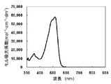
- FIG. 2 shows an absorption spectrum curve of the obtained spirobifluorene compound SP-1 (dye) in THF.
- the maximum absorption wavelength ( ⁇ max) of the spirobifluorene compound SP-1 was 515 nm.
- R3 (3,4'-dihexyl-2,2'-bithiophene) was dissolved in 80 ml of dry THF, and 11.2 ml of a 1.6 mol / L n-butyllithium hexane solution at ⁇ 78 ° C. in an argon atmosphere. The solution was added dropwise and stirred for 2 hours. Then, 6.324 g of tributyltin chloride was added, stirred at that temperature for 30 minutes, and further stirred overnight at room temperature. 300 ml of water was added to the reaction solvent, and the organic layer was extracted with diethyl ether and dried over magnesium sulfate. The solvent was distilled off under reduced pressure to obtain 8.39 g of B1.
- Example 2 As in Example 1, except that B1 was used instead of compound A1 and reacted with R2 to obtain B2, then reacted with N, N-dimethylformamide to obtain B3, and finally cyanoacetic acid To obtain the target spirobifluorene compound SP-2.
- ⁇ max of the obtained spirobifluorene compound SP-2 (dye) was 479 nm.
- a titanium oxide paste (semiconductor layer material) was prepared as follows.
- Commercially available titanium oxide powder (trade name: P25, manufactured by Nippon Aerosil Co., Ltd., average primary particle size: 21 nm) 5 g, 15 vol% acetic acid aqueous solution 20 ml, surfactant 0.1 ml (trade name: “Triton” (registered trademark) X-100, manufactured by Sigma-Aldrich Co., Ltd.) and 0.3 g of polyethylene glycol (molecular weight 20000) (manufactured by Wako Pure Chemical Industries, Ltd., product code: 168-11285) were mixed, and this mixture was stirred with a stirring mixer for about 1 hour. A titanium oxide paste was obtained.
- this titanium oxide paste was applied on a glass with FTO by a doctor blade method so that the film thickness was about 50 ⁇ m (application area: 10 mm ⁇ 10 mm). Thereafter, the glass with FTO coated with the titanium oxide paste was put in an electric furnace, baked at 450 ° C. for about 30 minutes in an air atmosphere, and naturally cooled to obtain a porous titanium oxide film on the glass with FTO. .
- a light scattering layer was formed on the titanium oxide film as follows.
- a titanium oxide paste having an average particle size of 400 nm (trade name: PST-400C, manufactured by JGC Catalysts & Chemicals Co., Ltd.) was applied to the above-described titanium oxide film at a thickness of 20 ⁇ m by screen printing. Then, the light-scattering layer on the titanium oxide film was obtained by baking for about 30 minutes at 450 degreeC in air
- a counter electrode was fabricated as follows. A platinum layer having an average film thickness of 1 ⁇ m was deposited as a catalyst layer on a soda lime glass plate (thickness: 1.1 mm) by a vacuum deposition method to obtain a counter electrode.
- (C) Cell assembly The semiconductor electrode after the dye adsorption treatment and the counter electrode were arranged so that the semiconductor layer and the catalyst layer face each other, thereby forming a cell before electrolyte injection. Next, a thermosetting resin film in which the electrolyte was allowed to penetrate into the gap between the semiconductor electrode and the counter electrode was thermocompression bonded to the outer periphery of the cell.
- (D) Injection of electrolyte An iodine-based electrolyte was injected into the above-described cell from the above-mentioned cut and allowed to penetrate between the semiconductor electrode and the counter electrode.
- the iodine-based electrolyte uses acetonitrile as a solvent, the concentration of iodine is 0.05 mol / L, the concentration of lithium iodide is 0.1 mol / L, 4-tert-butylpyridine is 0.025 mol / L, 1,2- A solution of dimethyl-3-propylimidazolium iodide at a concentration of 0.6 mol / L was used.
- Example 4 As in Example 3, except that the spirobifluorene dye SP-2 was used instead of the spirobifluorene dye SP-1, a photoelectric conversion element was produced. As a result of evaluating the photoelectric conversion characteristics of the obtained device, a photoelectric conversion efficiency of 4.6% could be obtained.
- a photoelectric conversion element having excellent photoelectric conversion efficiency and a semiconductor electrode used therefor can be obtained. It can.
- Such a photoelectric conversion element can be applied to a photoelectrochemical cell, and is particularly suitable for a solar cell. Further, the cost can be reduced compared to the case where a metal complex containing a noble metal is used.
- the photoelectric conversion element according to the present invention is suitably used as a photoelectrochemical cell, and can be used not only as a photoelectrochemical cell but also as a photosensor.
Abstract
L'invention concerne un colorant pour transducteur photoélectrique contenant un composé de spirobifluorène représenté par la formule (1). Le colorant présente d'excellentes caractéristiques de conversion photoélectrique, et est utilisé non seulement pour une électrode semi-conductrice de transducteur photoélectrique mais également pour un transducteur photoélectrique et une cellule photoélectrochimique. Dans la formule (1), R1 et R2 représentent chacun indépendamment un atome d'hydrogène, un groupe alkyle ou alcoxy substitué ou non substitué ou un groupe hydroxyle ; Z représente un groupe de liaison conjugué π ; et X représente un groupe organique comprenant un groupe acide.
Applications Claiming Priority (2)
| Application Number | Priority Date | Filing Date | Title |
|---|---|---|---|
| JP2011204756 | 2011-09-20 | ||
| JP2011-204756 | 2011-09-20 |
Publications (1)
| Publication Number | Publication Date |
|---|---|
| WO2013042699A1 true WO2013042699A1 (fr) | 2013-03-28 |
Family
ID=47914461
Family Applications (1)
| Application Number | Title | Priority Date | Filing Date |
|---|---|---|---|
| PCT/JP2012/073986 WO2013042699A1 (fr) | 2011-09-20 | 2012-09-20 | Composé de spirobifluorène, colorant pour transducteur photoélectrique, et transducteur photoélectrique les utilisant |
Country Status (1)
| Country | Link |
|---|---|
| WO (1) | WO2013042699A1 (fr) |
Cited By (5)
| Publication number | Priority date | Publication date | Assignee | Title |
|---|---|---|---|---|
| WO2021010425A1 (fr) | 2019-07-16 | 2021-01-21 | Ricoh Company, Ltd. | Module de photopile, dispositif électronique et module d'alimentation électrique |
| EP3839994A1 (fr) | 2019-11-28 | 2021-06-23 | Ricoh Company, Ltd. | Élément de conversion photoélectrique, module de conversion photoélectrique, dispositif électronique et module d'alimentation électrique |
| EP4064355A1 (fr) | 2021-03-23 | 2022-09-28 | Ricoh Company, Ltd. | Module de cellule solaire |
| WO2023008085A1 (fr) | 2021-07-29 | 2023-02-02 | Ricoh Company, Ltd. | Élément de conversion photoélectrique et module de cellules solaires |
| WO2023175466A1 (fr) | 2022-03-18 | 2023-09-21 | Ricoh Company, Ltd. | Élément de conversion photoélectrique, module de conversion photoélectrique, dispositif électronique et module de cellule solaire |
Citations (4)
| Publication number | Priority date | Publication date | Assignee | Title |
|---|---|---|---|---|
| JP2008204785A (ja) * | 2007-02-20 | 2008-09-04 | Mitsubishi Paper Mills Ltd | 光電変換材料、半導体電極並びにそれを用いた光電変換素子 |
| KR20100128255A (ko) * | 2009-05-27 | 2010-12-07 | 주식회사 동진쎄미켐 | 신규한 스파이로바이플루오렌계 염료 및 이의 제조방법 |
| US20110232763A1 (en) * | 2010-03-24 | 2011-09-29 | Samsung Sdi Co., Ltd. | Spirobifluorene-based compound and dye-sensitized solar cell using the same |
| WO2012029659A1 (fr) * | 2010-08-31 | 2012-03-08 | 綜研化学株式会社 | Nouveau composé fluorène, colorant pour cellule solaire à pigment photosensible utilisant le composé, électrode contenant ledit colorant et cellule solaire à pigment photosensible |
-
2012
- 2012-09-20 WO PCT/JP2012/073986 patent/WO2013042699A1/fr active Application Filing
Patent Citations (4)
| Publication number | Priority date | Publication date | Assignee | Title |
|---|---|---|---|---|
| JP2008204785A (ja) * | 2007-02-20 | 2008-09-04 | Mitsubishi Paper Mills Ltd | 光電変換材料、半導体電極並びにそれを用いた光電変換素子 |
| KR20100128255A (ko) * | 2009-05-27 | 2010-12-07 | 주식회사 동진쎄미켐 | 신규한 스파이로바이플루오렌계 염료 및 이의 제조방법 |
| US20110232763A1 (en) * | 2010-03-24 | 2011-09-29 | Samsung Sdi Co., Ltd. | Spirobifluorene-based compound and dye-sensitized solar cell using the same |
| WO2012029659A1 (fr) * | 2010-08-31 | 2012-03-08 | 綜研化学株式会社 | Nouveau composé fluorène, colorant pour cellule solaire à pigment photosensible utilisant le composé, électrode contenant ledit colorant et cellule solaire à pigment photosensible |
Non-Patent Citations (3)
| Title |
|---|
| CHO N. ET AL: "Novel organic sensitizers containing a bulky spirobifluorene unit for solar cell", TETRAHEDRON, vol. 65, no. 31, 2009, pages 6236 - 6243, XP002634165 * |
| LEE M.-W. ET AL: "Synthesis of organic dyes with linkers between 9,9-dimethylfluorenyl terminal and alpha-cyanoacrylic acid anchor, effect of the linkers on UV-Vis absorption spectra, and photovoltaic properties in dye-sensitized solar cells", BULLETIN OF THE KOREAN CHEMICAL SOCIETY, vol. 30, no. 10, 2009, pages 2269 - 2279, XP003030971 * |
| SHEN P. ET AL: "Efficient triphenylamine-based dyes featuring dual-role carbazole, fluorene and spirobifluorene moieties", ORGANIC ELECTRONICS, vol. 12, no. 1, 2011, pages 125 - 135, XP027576996 * |
Cited By (5)
| Publication number | Priority date | Publication date | Assignee | Title |
|---|---|---|---|---|
| WO2021010425A1 (fr) | 2019-07-16 | 2021-01-21 | Ricoh Company, Ltd. | Module de photopile, dispositif électronique et module d'alimentation électrique |
| EP3839994A1 (fr) | 2019-11-28 | 2021-06-23 | Ricoh Company, Ltd. | Élément de conversion photoélectrique, module de conversion photoélectrique, dispositif électronique et module d'alimentation électrique |
| EP4064355A1 (fr) | 2021-03-23 | 2022-09-28 | Ricoh Company, Ltd. | Module de cellule solaire |
| WO2023008085A1 (fr) | 2021-07-29 | 2023-02-02 | Ricoh Company, Ltd. | Élément de conversion photoélectrique et module de cellules solaires |
| WO2023175466A1 (fr) | 2022-03-18 | 2023-09-21 | Ricoh Company, Ltd. | Élément de conversion photoélectrique, module de conversion photoélectrique, dispositif électronique et module de cellule solaire |
Similar Documents
| Publication | Publication Date | Title |
|---|---|---|
| WO2013121835A1 (fr) | Dérivé de spirobifluorène, colorant pour éléments de conversion photoélectrique, électrode de semi-conducteur l'utilisant, élément de conversion photoélectrique et cellule photoélectrochimique | |
| KR101718198B1 (ko) | 금속 착물 색소, 광전 변환 소자, 색소 증감 태양 전지, 색소 증감 태양 전지용 색소 흡착 조성액, 색소 증감 태양 전지용 반도체 전극 및 색소 증감 태양 전지의 제조 방법 | |
| KR20130082489A (ko) | 신규한 티오펜계 염료 및 이의 제조방법 | |
| WO2013042699A1 (fr) | Composé de spirobifluorène, colorant pour transducteur photoélectrique, et transducteur photoélectrique les utilisant | |
| WO2012063753A1 (fr) | Composé indole, pigment à conversion photoélectrique associé, électrode semi-conductrice, élément à conversion photoélectrique et cellule électrophotochimique | |
| JP5620496B2 (ja) | 金属錯体色素、光電変換素子及び光電気化学電池 | |
| KR20100136931A (ko) | 신규한 유기염료 및 이의 제조방법 | |
| JP2014043401A (ja) | 金属錯体、およびそれを用いた色素増感太陽電池 | |
| WO2013042414A1 (fr) | Composé de dithiénopyrrole, colorant pour élément de conversion photoélectrique, électrode de semi-conducteur l'utilisant pour un élément de conversion photoélectrique et élément de conversion photoélectrique | |
| WO2012111610A1 (fr) | Thiazoles et leur utilisation | |
| JP2003017148A (ja) | 電解質組成物、光電変換素子及び光電気化学電池 | |
| JP4620286B2 (ja) | 電解質組成物、光電変換素子及び光電気化学電池 | |
| JP5816111B2 (ja) | 金属錯体色素組成物、光電変換素子及び光電気化学電池 | |
| JP2012051952A (ja) | 色素、光電変換素子及び光電気化学電池 | |
| WO2012096134A1 (fr) | Dérivé d'alcyne et son utilisation | |
| JP5235952B2 (ja) | ツイッターイオン型有機塩 | |
| WO2011083527A1 (fr) | Colorant pour conversion photoélectrique, électrode à semi-conducteurs, élément de conversion photoélectrique, photopile et nouveau composé de pyrroline | |
| JP4520727B2 (ja) | ピロリジニウム塩、電解質組成物、光電変換素子及び光化学電池 | |
| KR101587829B1 (ko) | 염료감응 태양전지 및 이에 사용되는 유기염료 | |
| WO2011145321A1 (fr) | Composé de maléimide, tautomère ou stéréoisomère de celui-ci, colorant pour conversion photoélectrique, et électrode à semi-conducteur, élément de conversion photoélectrique et cellule photoélectrochimique qui sont fabriqués en utilisant ceux-ci | |
| WO2015190398A1 (fr) | Élément de conversion photoélectrique, cellule solaire à colorant, colorant complexe à base de ruthénium, solution de colorant, et composé de bipyridine | |
| JP6371908B2 (ja) | 光電変換素子、色素増感太陽電池、金属錯体色素、色素溶液および酸化物半導体電極 | |
| KR101465454B1 (ko) | 염료감응 태양전지용 유기염료 및 이를 포함하는 염료감응 태양전지 | |
| JP5587070B2 (ja) | 第四級アンモニウム塩、並びにこれを用いた電解質組成物、光電変換素子及び光化学電池 | |
| WO2018047498A1 (fr) | Élément de conversion photoélectrique, cellule solaire à colorant et composé complexe de dipyrrométhene |
Legal Events
| Date | Code | Title | Description |
|---|---|---|---|
| 121 | Ep: the epo has been informed by wipo that ep was designated in this application |
Ref document number: 12833519 Country of ref document: EP Kind code of ref document: A1 |
|
| NENP | Non-entry into the national phase |
Ref country code: DE |
|
| 122 | Ep: pct application non-entry in european phase |
Ref document number: 12833519 Country of ref document: EP Kind code of ref document: A1 |
|
| NENP | Non-entry into the national phase |
Ref country code: JP |