WO2013035683A1 - 機能性フィルムおよび機能性フィルムの製造方法 - Google Patents
機能性フィルムおよび機能性フィルムの製造方法 Download PDFInfo
- Publication number
- WO2013035683A1 WO2013035683A1 PCT/JP2012/072432 JP2012072432W WO2013035683A1 WO 2013035683 A1 WO2013035683 A1 WO 2013035683A1 JP 2012072432 W JP2012072432 W JP 2012072432W WO 2013035683 A1 WO2013035683 A1 WO 2013035683A1
- Authority
- WO
- WIPO (PCT)
- Prior art keywords
- film
- region
- support
- inorganic
- inorganic film
- Prior art date
- Legal status (The legal status is an assumption and is not a legal conclusion. Google has not performed a legal analysis and makes no representation as to the accuracy of the status listed.)
- Ceased
Links
Images


Classifications
-
- C—CHEMISTRY; METALLURGY
- C23—COATING METALLIC MATERIAL; COATING MATERIAL WITH METALLIC MATERIAL; CHEMICAL SURFACE TREATMENT; DIFFUSION TREATMENT OF METALLIC MATERIAL; COATING BY VACUUM EVAPORATION, BY SPUTTERING, BY ION IMPLANTATION OR BY CHEMICAL VAPOUR DEPOSITION, IN GENERAL; INHIBITING CORROSION OF METALLIC MATERIAL OR INCRUSTATION IN GENERAL
- C23C—COATING METALLIC MATERIAL; COATING MATERIAL WITH METALLIC MATERIAL; SURFACE TREATMENT OF METALLIC MATERIAL BY DIFFUSION INTO THE SURFACE, BY CHEMICAL CONVERSION OR SUBSTITUTION; COATING BY VACUUM EVAPORATION, BY SPUTTERING, BY ION IMPLANTATION OR BY CHEMICAL VAPOUR DEPOSITION, IN GENERAL
- C23C16/00—Chemical coating by decomposition of gaseous compounds, without leaving reaction products of surface material in the coating, i.e. chemical vapour deposition [CVD] processes
- C23C16/22—Chemical coating by decomposition of gaseous compounds, without leaving reaction products of surface material in the coating, i.e. chemical vapour deposition [CVD] processes characterised by the deposition of inorganic material, other than metallic material
- C23C16/30—Deposition of compounds, mixtures or solid solutions, e.g. borides, carbides, nitrides
- C23C16/34—Nitrides
- C23C16/345—Silicon nitride
-
- C—CHEMISTRY; METALLURGY
- C23—COATING METALLIC MATERIAL; COATING MATERIAL WITH METALLIC MATERIAL; CHEMICAL SURFACE TREATMENT; DIFFUSION TREATMENT OF METALLIC MATERIAL; COATING BY VACUUM EVAPORATION, BY SPUTTERING, BY ION IMPLANTATION OR BY CHEMICAL VAPOUR DEPOSITION, IN GENERAL; INHIBITING CORROSION OF METALLIC MATERIAL OR INCRUSTATION IN GENERAL
- C23C—COATING METALLIC MATERIAL; COATING MATERIAL WITH METALLIC MATERIAL; SURFACE TREATMENT OF METALLIC MATERIAL BY DIFFUSION INTO THE SURFACE, BY CHEMICAL CONVERSION OR SUBSTITUTION; COATING BY VACUUM EVAPORATION, BY SPUTTERING, BY ION IMPLANTATION OR BY CHEMICAL VAPOUR DEPOSITION, IN GENERAL
- C23C16/00—Chemical coating by decomposition of gaseous compounds, without leaving reaction products of surface material in the coating, i.e. chemical vapour deposition [CVD] processes
- C23C16/44—Chemical coating by decomposition of gaseous compounds, without leaving reaction products of surface material in the coating, i.e. chemical vapour deposition [CVD] processes characterised by the method of coating
- C23C16/50—Chemical coating by decomposition of gaseous compounds, without leaving reaction products of surface material in the coating, i.e. chemical vapour deposition [CVD] processes characterised by the method of coating using electric discharges
- C23C16/505—Chemical coating by decomposition of gaseous compounds, without leaving reaction products of surface material in the coating, i.e. chemical vapour deposition [CVD] processes characterised by the method of coating using electric discharges using radio frequency discharges
- C23C16/509—Chemical coating by decomposition of gaseous compounds, without leaving reaction products of surface material in the coating, i.e. chemical vapour deposition [CVD] processes characterised by the method of coating using electric discharges using radio frequency discharges using internal electrodes
-
- C—CHEMISTRY; METALLURGY
- C23—COATING METALLIC MATERIAL; COATING MATERIAL WITH METALLIC MATERIAL; CHEMICAL SURFACE TREATMENT; DIFFUSION TREATMENT OF METALLIC MATERIAL; COATING BY VACUUM EVAPORATION, BY SPUTTERING, BY ION IMPLANTATION OR BY CHEMICAL VAPOUR DEPOSITION, IN GENERAL; INHIBITING CORROSION OF METALLIC MATERIAL OR INCRUSTATION IN GENERAL
- C23C—COATING METALLIC MATERIAL; COATING MATERIAL WITH METALLIC MATERIAL; SURFACE TREATMENT OF METALLIC MATERIAL BY DIFFUSION INTO THE SURFACE, BY CHEMICAL CONVERSION OR SUBSTITUTION; COATING BY VACUUM EVAPORATION, BY SPUTTERING, BY ION IMPLANTATION OR BY CHEMICAL VAPOUR DEPOSITION, IN GENERAL
- C23C16/00—Chemical coating by decomposition of gaseous compounds, without leaving reaction products of surface material in the coating, i.e. chemical vapour deposition [CVD] processes
- C23C16/44—Chemical coating by decomposition of gaseous compounds, without leaving reaction products of surface material in the coating, i.e. chemical vapour deposition [CVD] processes characterised by the method of coating
- C23C16/54—Apparatus specially adapted for continuous coating
- C23C16/545—Apparatus specially adapted for continuous coating for coating elongated substrates
Definitions
- the present invention relates to a functional film such as a gas barrier film and a method for producing the functional film.
- Gas barrier films are used in parts and parts that require moisture-proof properties in optical devices, display devices such as liquid crystal displays and organic EL displays, various semiconductor devices, and various devices such as solar cells. Gas barrier films are also used for packaging materials for packaging food, electronic parts, and the like.
- the gas barrier film generally has a structure in which a plastic film such as a polyethylene terephthalate (PET) film is used as a support (substrate) and a film (gas barrier film) that exhibits gas barrier properties is formed thereon.
- PET polyethylene terephthalate
- inorganic films films made of inorganic compounds
- films exhibiting gas barrier properties Specifically, inorganic films such as silicon nitride, silicon oxide, silicon oxynitride, and aluminum oxide are used for the gas barrier film.
- Such a gas barrier film is required not only to have excellent gas barrier properties but also to have good adhesion of the inorganic film.
- a gas barrier film in which an inorganic film having gas barrier properties is formed if there are defects such as cracks or peeling in the inorganic membrane, water vapor permeates from here and the gas barrier properties are greatly reduced. Therefore, in order to obtain a high gas barrier property, the inorganic film formed on the gas barrier film is required to have no (small) cracks, peeling, defective portions, and the like.
- various proposals have been made for gas barrier films formed by forming an inorganic film having gas barrier properties.
- Patent Document 1 describes a gas barrier film in which silicon oxynitride is formed as an inorganic film having gas barrier properties on a support (synthetic resin sheet), and the density distribution of the inorganic film is adjusted.
- the density of the inorganic film (silicon oxynitride film) near the interface on the support side is A
- the density of the region excluding the vicinity of the interface is B
- the inorganic film is 0.905.
- a gas barrier film that is a single deposited layer having a relationship of ⁇ A / B ⁇ 1.000 and continuous in the film thickness direction.
- the inorganic film described in Patent Literature 1 has a density distribution as described above, so that the structure inside the inorganic film is not simple but complicated.
- the structure inside the inorganic film is complicated by the presence of portions having different densities inside the inorganic film.
- the gas barrier film described in Patent Document 1 exhibits a function of hindering the permeation of water vapor due to the complicated internal structure of the inorganic film, and exhibits a high gas barrier property.
- the entire film may be formed when the required film thickness is formed.
- the stress balance is easily lost, and the film is likely to crack or peel off. This tendency becomes higher as the dense inorganic film with high gas barrier property is obtained.
- An object of the present invention is to solve the problems of the prior art, and has excellent performance in a functional film such as a gas barrier film formed by forming an inorganic film on a support such as a plastic film. Not only that, it is possible to suitably produce a functional film that significantly reduces cracks, delamination and defects in the inorganic film, and also has excellent adhesion of the inorganic film, and such a high-performance functional film. It is to provide a manufacturing method.
- the functional film of the present invention is a functional film having a support and an inorganic film formed on the support, and the inorganic film includes the region B and this film.
- the inorganic film when the density of the region A is a and the density of the region B is b, it is preferable to satisfy “0.6 ⁇ b / a ⁇ 1”.
- the inorganic film preferably contains silicon and nitrogen.
- the thickness of the layered structure of region B-region A-region B is preferably 10 to 200 nm.
- the inorganic film preferably has a gas barrier property.
- the manufacturing method of the functional film of this invention forms the same inorganic film
- the surface temperature of the inorganic film should not be lower than 20 ° C. before being exposed to plasma by the next film forming means.
- the film forming means preferably forms the inorganic film while supplying bias power to the non-inorganic film forming surface side of the support. Moreover, it is preferable to form an inorganic film by a plurality of film forming means while transporting the long support in the longitudinal direction. Moreover, it is preferable that the support body formed by feeding the support body from the support roll formed by winding the long support body and transporting it to form the inorganic film is wound again in a roll shape. In addition, a long drum is wound around a circumferential surface of a long support, and a cylindrical drum is conveyed to rotate the drum. It is preferable to be disposed so as to face the peripheral surface.
- the film forming means preferably forms an inorganic film containing silicon and nitrogen as the inorganic film. Further, the film forming means preferably forms an inorganic film having gas barrier properties as the inorganic film.
- the functional film of the present invention having the above configuration is a functional film having an inorganic film that expresses a target function on a support such as a plastic film, and the inorganic film is mainly inorganic in the thickness direction. It has a region B for forming a film and a region A that is thinner and denser than this region B, and further has at least one layer B-region A-region B stacked structure in the thickness direction.
- Such a functional film of the present invention has a high-density region A mainly between the regions B where the inorganic film is formed. Therefore, the entire region has the same thickness and the same thickness of the inorganic film (one-layer inorganic film). High performance compared to membrane).
- the film stress of the entire inorganic film can be reduced / controlled by having a sandwich structure having a high-density region A between the regions B mainly forming the inorganic film. Therefore, even with dense and high-density inorganic films, it is possible to greatly prevent the occurrence of cracks and peeling due to the unbalance of film stress, etc., and the adhesion between the inorganic film and the support and the adhesion inside the inorganic film Also excellent. Furthermore, even if cracks, separation, defects, etc. occur during the formation of the inorganic film, the initial state can be once restored when the region changes, so that cracks, defects, etc. can be prevented from growing greatly.
- the present invention it is possible to obtain a high-quality functional film having high performance, high adhesion of the inorganic film, low film stress, and greatly reducing cracks, peeling, defects and the like. Therefore, for example, by using the functional film of the present invention for a gas barrier film, a gas barrier film having excellent gas barrier performance can be obtained.
- FIG. 1 conceptually shows an example of the functional film of the present invention.
- the functional film 10 of the present invention has a support Z and an inorganic film 12 formed on the support Z.
- the functional film 10 of the present invention is not limited to the one having only the support Z and the inorganic film 12. That is, as long as the functional film of the present invention has the support Z and the inorganic film 12 formed thereon, various layer configurations can be used.
- an organic film as an underlayer for forming the high-quality inorganic film 12 may be provided under the inorganic film 12. That is, the functional film 10 of the present invention may be used as the support Z in which a plastic film or the like is used as a base material and an organic film as a base layer is formed thereon.
- a layer (film) for obtaining various functions such as a protective layer, an adhesive layer, a light reflecting layer, a light shielding layer, a planarizing layer, a buffer layer, and a stress relaxation layer is formed instead of the organic film.
- An object may be used as the support Z. Or you may use the thing in which the layer for obtaining these various functions is formed in the lower layer and / or upper layer of an organic film as the support body Z.
- the functional film of the present invention may be one in which an organic film as a protective layer is formed on the inorganic film 12.
- a plurality of laminated structures of an organic film as a base layer and the inorganic film 12 formed on the surface of the organic film may be repeatedly provided.
- a plurality of laminated structures of the base organic film and the inorganic film 12 may be repeatedly provided, and an organic film as a protective layer may be formed on the uppermost layer.
- each inorganic film 12 may be the same or different.
- the organic films may be the same or different.
- the functional film 10 of the present invention has an organic film as a base layer of the inorganic film 12 on the surface, like the support Z in which an organic film is formed on a substrate such as a plastic film. Is preferred. Moreover, it is preferable that the functional film 10 of this invention has an organic film as a protective layer in the uppermost layer.
- the material for forming the organic film is not particularly limited, and various known organic compounds (resins / polymer compounds) can be used. Specifically, polyester, acrylic resin, methacrylic resin, methacrylic acid-maleic acid copolymer, polystyrene, transparent fluororesin, polyimide, fluorinated polyimide, polyamide, polyamideimide, polyetherimide, cellulose acylate, polyurethane, poly Ether ether ketone, polycarbonate, alicyclic polyolefin, polyarylate, polyethersulfone, polysulfone, fluorene ring modified polycarbonate, alicyclic modified polycarbonate, fluorene ring modified polyester, acryloyl compound, thermoplastic resin, or polysiloxane, etc.
- polyester acrylic resin, methacrylic resin, methacrylic acid-maleic acid copolymer, polystyrene, transparent fluororesin, polyimide, fluorinated polyimide, polyamide,
- An organic silicon compound film is preferably exemplified.
- an organic film composed of a radical polymerizable compound and / or a polymer of a cationic polymerizable compound having an ether group as a functional group is preferable from the viewpoint of excellent strength and the like.
- an organic film containing an acrylic resin or a methacrylic resin containing a acrylate and / or methacrylate monomer or oligomer polymer as a main component in terms of low refractive index, excellent optical properties, etc. are preferably exemplified.
- the support (base material / substrate) Z is not particularly limited, and any of various sheet materials that can form the inorganic film 12 by plasma CVD can be used.
- plastic films made of organic substances such as polyethylene terephthalate (PET), polyethylene naphthalate (PEN), polyethylene, polypropylene, polystyrene, polyamide, polyvinyl chloride, polycarbonate, polyacrylonitrile, polyimide, polyacrylate, polymethacrylate ( Resin film) can be suitably used as the support Z.
- PET polyethylene terephthalate
- PEN polyethylene naphthalate
- polyethylene polypropylene
- polystyrene polyamide
- polyvinyl chloride polycarbonate
- polyacrylonitrile polyacrylonitrile
- polyimide polyacrylate
- polymethacrylate Resin film
- the functional film 10 of the present invention is obtained by forming the inorganic film 12 on the support Z.
- the inorganic film 12 is a film made of an inorganic compound.
- the inorganic film 12 is a film made of the same inorganic compound in the entire thickness direction, but has a laminated structure of two types of regions (two types of layers) having different densities.
- the inorganic film 12 is a film composed of five layers (five regions) of the layers 12a to 12e.
- the layers 12b and 12d are thinner than the layers 12a, 12c and 12e, and are dense and dense.
- each layer forming the inorganic film 12 is not a single independent film having an interface except that the density of adjacent layers is different. It is formed integrally. That is, the inorganic film 12 is a single film having five regions.
- the layers 12a, 12c and 12e are the region B in the present invention, and mainly constitute the inorganic film 12.
- the layers 12b and 12d are the region A in the present invention in which the layer 12b and 12d have a higher density and a smaller thickness than the region B.
- the region A may have a region in which the density changes continuously (gradually) in the thickness direction.
- the density of the region A may change continuously throughout the thickness direction.
- the layers 12a, 12c and 12e have basically the same density, and similarly, the layers 12b and 12d have basically the same density.
- the functional film 10 in the illustrated example has a layered structure of region B-region A-region B in the present invention, a layered structure of layer 12a-layer 12b-layer 12c, and a layered structure of layer 12c-layer 12d-layer 12e. Has two, with structure.
- the functional film of the present invention has a laminated structure (region B-region A-layer B laminated structure) in which such a dense and high-density region A is mainly sandwiched between regions B where the inorganic film 12 is formed.
- a laminated structure region B-region A-layer B laminated structure
- the functional film of the present invention has this configuration, the film stress of the entire inorganic film can be reduced / controlled by the buffering effect of the laminated structure. Therefore, even if the inorganic film 12 is dense and dense, it is possible to greatly prevent the occurrence of cracks and peeling due to the loss of the balance of film stress, and the adhesion between the inorganic film 12 and the support Z is also improved. It can be improved.
- the region A is a high-density region formed by exposing the surface of the inorganic film formed by the upstream film forming unit to the plasma again by the downstream film forming unit. Therefore, the adhesiveness between the region A and the region B, that is, the adhesiveness inside the inorganic film 12 is also high.
- the inorganic film 12 is basically formed (deposited) by plasma CVD. Even if cracks, delamination, defects, or the like occur in the inorganic film 12 during the formation, the inorganic film 12 is once formed when the region changes. Since it returns to the initial state of the film (because it can be reset), it is possible to prevent cracks and defects from growing greatly.
- the inorganic film 12 has a laminated structure in which the high-density region A is mainly sandwiched between the regions B where the inorganic film 12 is formed, a single-layer structure having the same thickness (the entire density in the thickness direction is uniform) ) Exhibit very high performance compared to the inorganic film.
- the present invention it has high performance, the adhesiveness of the inorganic film 12 is good, the adhesiveness between the support Z and the support Z is high, and cracks, peeling, defects, etc. are greatly reduced.
- a high-quality functional film can be obtained. Therefore, for example, by using the functional film of the present invention for a gas barrier film, a gas barrier film having high strength and excellent gas barrier performance can be obtained.
- the configuration of the inorganic film 12 is not limited to the illustrated example. That is, the functional film of the present invention has various regions as long as it has regions A and B alternately in the thickness direction and one or more laminated structures of region B-region A-region B. Configuration is available.
- the inorganic film 12 of the functional film 10 shown in FIG. 1 may be an inorganic film composed of three layers (three regions) of the layers 12a to 12c.
- the inorganic film 12 of the functional film 10 shown in FIG. 1 may be a seven-layered inorganic film in which a region A and a region B are further formed on the layer 12e.
- An inorganic film composed of 9 or more layers may be used.
- the lowermost layer (lowermost layer) and the uppermost layer (uppermost layer) of the inorganic film 12 are mainly regions B where the inorganic film 12 is formed.
- the density of the region A and the region B is not particularly limited.
- the density of the region A and the region B may be appropriately set according to the use of the functional film 10 and the inorganic compound forming the inorganic film 12.
- the inorganic film 12 when the density of the region A is a and the density of the region B is b, the inorganic film 12 preferably satisfies “0.6 ⁇ b / a ⁇ 1”.
- the inorganic film 12 satisfies “0.6 ⁇ b / a ⁇ 1”.
- preferable results are obtained in terms of the stress balance of the film, the adhesive strength with the support Z, the durability (such as the effect of suppressing change over time), and the like. Can be obtained.
- the thickness of the inorganic film 12 is not particularly limited.
- the thickness of the inorganic film 12 is appropriately determined according to the use of the functional film 10, the performance required for the functional film 10 (inorganic film 12), the inorganic compound forming the inorganic film 12, the required productivity, and the like. , You can set.
- the thickness of the region B-region A-region B is preferably 10 to 200 nm. By having such a configuration, favorable results can be obtained in terms of stress balance of the film, durability (such as an effect of suppressing change over time), productivity (such as an apparatus configuration), and the like.
- the regions A may have the same or different thickness.
- the regions B may have the same or different thickness.
- the thickness ratio between the region A and the region B is not particularly limited. For the same reason as described above, the thickness of the region A is 3 to 30% of the thickness of the adjacent region B. Is preferred.
- the thickness of the laminated structure is set by setting a region where a constant density assumed as the inorganic film 12 is continuous in the thickness direction as a region B and a region other than this as the region A.
- the inorganic compound that forms the inorganic film 12 (the inorganic compound that is the main component of the inorganic film 12) is not particularly limited.
- the inorganic compound that forms the inorganic film 12 various inorganic compounds that exhibit a required function can be used depending on the application of the functional film 10.
- Examples include metal oxides such as aluminum oxide, magnesium oxide, tantalum oxide, zirconium oxide, titanium oxide, and indium tin oxide (ITO); metal nitrides such as aluminum nitride; metal carbides such as aluminum carbide; silicon oxide, oxynitride Silicon oxides such as silicon, silicon oxycarbide and silicon oxynitride carbide; silicon nitrides such as silicon nitride and silicon nitride carbide; silicon carbides such as silicon carbide; hydrides thereof; mixtures of two or more of these; and these
- membrane which consists of inorganic compounds, such as these hydrogen containing materials, is illustrated suitably.
- the functional film 10 of the present invention has an inorganic film 12 with extremely few cracks, peeling, defects and the like. Therefore, it is suitably used for applications where performance deterioration due to these is large, and particularly, it is suitably used for gas barrier films. Therefore, the inorganic film 12 is preferably a film having gas barrier properties.
- the inorganic compound that forms the inorganic film 12 is preferably an inorganic compound that exhibits gas barrier properties such as silicon nitride, silicon oxide, silicon oxynitride, and aluminum oxide.
- inorganic compounds containing silicon and nitrogen such as silicon nitride and silicon oxynitride are particularly suitable.
- FIG. 2 an example of the manufacturing method of the functional film of this invention is implemented, and an example of the plasma CVD apparatus which manufactures the functional film 10 of this invention is shown notionally.
- a plasma CVD apparatus 14 (hereinafter, referred to as a CVD apparatus 14) shown in FIG. 2 conveys a long support Z (web-shaped film original fabric) in the longitudinal direction, and has a capacity on the surface of the support Z.
- the inorganic film 12 is formed (deposited) by coupled plasma CVD (CCP (Capacitively Coupled Plasma) -CVD) to produce the functional film 10 of the present invention such as a gas barrier film or various optical films.
- CCP Capacitively Coupled Plasma
- the formation of the inorganic film 12 is not limited to being performed by CCP-CVD, and various types of plasma CVD such as ICP-CVD (inductively coupled plasma CVD) can be used. is there.
- the CVD apparatus 14 shown in FIG. 2 continuously feeds the support Z from a support roll Zr formed by winding a long support Z into a roll shape, and continuously conveys the support Z in the longitudinal direction. 12 is formed, and the support Z on which the inorganic film 12 is formed is wound around the take-up shaft 16 again in a roll shape, so that a so-called roll-to-roll (hereinafter referred to as RtoR) is used to make inorganic An apparatus for forming a film.
- RtoR roll-to-roll
- the manufacturing method of this invention is not limited to what utilizes RtoR using the elongate support body Z.
- the present invention provides a cut sheet-like support Z as long as the inorganic film 12 is formed by a plurality of plasma CVD means arranged in the transport direction while transporting the support Z that forms the inorganic film 12.
- the inorganic film 12 may be formed.
- the CVD apparatus 14 includes a supply chamber 18, a film formation chamber 20, and a winding chamber 24.
- the CVD apparatus 14 includes various sensors, a pair of transport rollers, and a guide member that regulates the position of the support Z in the width direction.
- Various members of an apparatus for performing plasma CVD with RtoR may be provided on a long support Z such as the above member (conveying means).
- the supply chamber 18 includes a rotating shaft 28, a guide roller 30, and a vacuum exhaust unit 32.
- the support roll Zr around which the support Z is wound is mounted on the rotating shaft 28 of the supply chamber 18.
- the support Z is pulled out from the support roll Zr, passes through the film forming chamber 20 from the supply chamber 18, and reaches the winding shaft 16 of the winding chamber 24.
- the paper is passed through the transport path (through a predetermined transport path).
- the feeding of the support Z from the support roll Zr and the winding of the support Z on the winding shaft 16 of the winding chamber 24 are performed in synchronization, so that the long support Z is formed.
- the inorganic film 12 is continuously formed on the support Z by CCP-CVD in the film forming chamber 20 while being transported in the longitudinal direction along a predetermined transport path.
- the supply chamber 18 rotates the rotary shaft 28 counterclockwise in the figure by a drive source (not shown), feeds the support Z from the support roll Zr, guides a predetermined path by the guide roller 30, and supports the support Z. From the slit 34 a provided in the partition wall 34 to the film forming chamber 20.
- a vacuum exhaust means 32 is provided in the supply chamber 18, and a vacuum exhaust means 70 is provided in the winding chamber 24.
- the pressure in the supply chamber 18 and the winding chamber 24 is maintained at a predetermined pressure corresponding to the pressure (formation pressure) in the film formation chamber 20 described later by the respective vacuum exhaust means. . This prevents the pressure in the adjacent chamber from affecting the pressure in the film forming chamber 20 (that is, formation in the film forming chamber 20).
- the vacuum evacuation means 32 is not particularly limited, and includes a vacuum pump such as a turbo pump, a mechanical booster pump, a dry pump, and a rotary pump, an auxiliary means such as a cryocoil, a means for adjusting the ultimate vacuum level and the exhaust amount, and the like.
- a vacuum pump such as a turbo pump, a mechanical booster pump, a dry pump, and a rotary pump
- an auxiliary means such as a cryocoil
- a means for adjusting the ultimate vacuum level and the exhaust amount and the like.
- Various known (vacuum) evacuation means used in the vacuum forming apparatus can be used. In this regard, the same applies to the other vacuum exhaust means 60 and 70 described later.
- the support Z is guided by the guide roller 30 and is conveyed from the slit 34 a of the partition wall 34 to the film forming chamber 20.
- the film forming chamber 20 is for forming (depositing) the inorganic film 12 formed in the region A and the region B on the surface of the support Z by CCP-CVD.
- the region B mainly constitutes the inorganic film 12, and the region A is thinner and denser than the region B.
- the film forming chamber 20 includes a drum 38, guide rollers 42, 46, 48 and 50, three film forming means 52a, 52b and 52c for forming the inorganic film 12, a bias power source 58, and vacuum exhaust. Means 60.
- the CVD apparatus 14 in the illustrated example is arranged in the transport direction of the support Z and has three film forming means.
- the production method of the present invention is not limited to this, and the number of film forming means may be two, or four or more film forming means may be provided.
- the drum 38 of the film forming chamber 20 is a hollow cylindrical member, and rotates in the direction of the arrow (clockwise) in the drawing around a rotation axis that coincides with the cylinder at the center line.
- the drum 38 is rotated by a driving source (not shown) after the support Z guided by the guide rollers 42 and 46 is hung on a predetermined area on the surface (around a predetermined winding angle).
- the drum 38 conveys the support Z in the longitudinal direction while being positioned at a predetermined position.
- the drum 38 that is wound around and supported by the support Z also functions as a counter electrode in CCP-CVD. That is, an electrode pair for performing film formation by CCP-CVD is formed by the drum 38 and a shower electrode 40 (film formation electrode) of each film formation means described later. Therefore, as a preferred embodiment, the drum 38 is connected to a bias power source 58 for supplying bias power.
- the film forming means for performing the manufacturing method of the present invention is not limited to this, and may be grounded without having the bias power source 58. Alternatively, the connection with the bias power source and the ground may be switched.
- the drum 38 preferably has a temperature adjusting means for adjusting the temperature of the peripheral surface that supports the support Z in order to cool and heat the support Z.
- Each of the film forming means 52a, 52b and 52c forms the inorganic film 12 by CCP-CVD on the support Z which is wound around the drum 38 and conveyed.
- the film forming units 52 a, 52 b and 52 c basically have the same configuration, and include a shower electrode 40, a high frequency power supply 54, and a gas supply unit 56.
- the shower electrode 40 is a known shower electrode (shower plate) used for film formation by CCP-CVD, in which a raw material gas is injected from the opposing surface of the support Z.
- the shower electrode 40 and the drum 38 constitute an electrode pair for performing CCP-CVD as described above.
- the shower electrode 40 has, for example, a substantially rectangular parallelepiped shape in which one surface is disposed facing the drum 38 (that is, the support Z) and a space (gas supply space) is formed therein.
- a large number of gas supply holes communicating with the internal space are formed on the surface of the shower electrode 40 facing the drum 38.
- the surface of the shower electrode 40 facing (facing) the drum 38 is a concave curved surface so as to be parallel to the surface of the drum 38. That is, the surface of the shower electrode 40 facing the drum 38 is a concave curved surface so that the distance between the drum 38 and the shower electrode is uniform over the entire surface.
- the shower electrodes 40 of the respective film forming means are arranged in the conveying direction of the support Z, that is, the rotating direction of the drum 38. That is, in the illustrated CVD apparatus 14, the film forming chamber 20 forms one inorganic film 12 by three film forming means by plasma CVD. Accordingly, the support Z is wound around the drum 38 and conveyed, so that the same inorganic film is formed three times at maximum by CCP-CVD, and the inorganic film 12 is formed on the surface.
- the gas supply means 56 is a known gas supply means used in a vacuum forming apparatus such as a plasma CVD apparatus.
- the gas supply means 56 supplies a source gas to the internal space of the shower electrode 40.
- a large number of gas supply holes communicating with the internal space are formed on the surface of the shower electrode 40 facing the drum 38. Therefore, the source gas supplied to the shower electrode 40 is supplied between the shower electrode 40 and the drum 38 through the gas supply hole.
- the source gas (process gas / material gas) supplied by the gas supply means 56 may be a known gas corresponding to the inorganic film 12 to be formed.
- the gas supply means 56 supplies silane gas, ammonia gas, and nitrogen gas (or hydrogen gas) as an example.
- the high-frequency power source 54 is a power source that supplies plasma excitation power to the shower electrode 40 that is a film-forming electrode in CCP-CVD.
- the high-frequency power source 54 is a known high-frequency power source used in various plasma CVD apparatuses such as a power source that supplies high-frequency power of 13.56 MHz.
- the bias power source 58 is a power source that supplies bias power (applies a bias potential) to the drum 38 that functions as a counter electrode in CCP-CVD.
- the bias power source 58 is also a known power source used in various plasma CVD apparatuses.
- the vacuum evacuation means 60 is for exhausting the inside of the forming chamber to maintain a predetermined pressure for film formation by plasma CVD. As described above, the known vacuum evacuation means used in the vacuum forming apparatus. It is.
- the film forming conditions of the inorganic film 12 such as the conveyance speed of the support Z, the forming pressure, the supply amount of the source gas, and the strength of the plasma excitation power. That is, the film formation conditions may be appropriately set according to the type and thickness of the inorganic film 12 to be formed, the type of the support Z, and the like, as in the case of film formation by normal plasma CVD.
- the film forming means 52a, 52b and 52c basically perform film formation under the same film formation conditions.
- the present invention is not limited to this, and when forming the inorganic film 12, if necessary, one or more of the film forming units 52a, 52b, and 52c can be used to set other film forming units and film forming conditions. You may change it.
- the support Z is sequentially formed with the inorganic film 12 by the three film forming means 52a, 52b and 52c, and the inorganic film 12 is formed. That is, when the support Z is transported to the film forming chamber 20, first, in the film forming region (the region where the shower electrode 40 and the drum 38 (support Z) face each other) in the film forming unit 52a, the support Z is inorganic. A film 12 is formed, and a layer 12 a that is a region B mainly constituting the inorganic film 12 is formed.
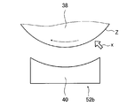
- the support Z on which the layer 12a is formed is transported to a film forming region in the film forming means 52b as conceptually shown in FIG.
- the film forming unit 52b first, the surface of the layer 12a, which is an inorganic film previously formed by the film forming unit 52a, is near the entrance of the film forming region indicated by the arrow x in FIG. In the vicinity of the most upstream part of the plasma, it is exposed to plasma again. This contact with plasma promotes so-called migration on the surface of the layer 12a.
- a high-density and dense inorganic film that is, the layer 12b which is the region A is slightly formed on the surface of the layer 12a, and then the region B mainly constituting the inorganic film 12 is formed thereon.
- a layer 12c is formed.
- plasma is strongly drawn into the layer 12a by performing film formation while supplying bias power to the drum 38 which is a counter electrode of CCP-CVD. Therefore, the effect of exposing the surface of this layer 12a to plasma is increased. As a result, the layer 12b becomes a very dense and dense inorganic film.
- the support Z on which the layers 12b and 12c are formed is then transported to the film forming region in the film forming means 52c.
- the surface of the layer 12c which is an inorganic film previously formed by the film forming means 52b, is exposed to plasma again in the vicinity of the entrance of the film forming region.
- a high-density inorganic film that is, the layer 12d as the region A is first slightly formed on the surface of the layer 12c, and then the inorganic film 12 is mainly formed thereon.
- a layer 12e which is a region B to be formed is formed.
- the regions A and B shown in FIG. 1 are alternately stacked, and are composed of five layers (regions) of the layer 12a to the layer 12e having two stacked configurations of region B-region A-region B.
- An inorganic film 12 is formed.
- the surface temperature of the inorganic film does not become 20 ° C. or lower until the film is exposed to the plasma by the downstream film forming means. It is important to make it.
- the surface temperature of the inorganic film is maintained above 20 ° C. until it is exposed to plasma by the next film forming means. That is, in the illustrated example, after the layer 12a is formed by the film forming unit 52a, the surface temperature of the layer 12a is kept from being 20 ° C. or lower until the layer 12a is exposed to plasma by the film forming unit 52b.
- the surface temperature of the layer 12c is set not to be 20 ° C. or lower until the layer 12c is exposed to plasma by the film forming unit 52c.
- the surface temperature of the inorganic film remains after the inorganic film is formed. If too low, migration of the inorganic film is not promoted even if the surface of the inorganic film is exposed to plasma by the downstream film forming means. As a result, the high-density region A cannot be formed on the surface of the region B, and the entire region becomes a normal inorganic film having substantially the same density. In contrast, after the formation of the inorganic film by the upstream film forming means, the surface temperature of the inorganic film is made to exceed 20 ° C.
- the inorganic film is formed after the inorganic film is formed by the upstream film forming unit and then exposed to the plasma by the downstream film forming unit in that the higher density region A can be stably formed.
- the surface temperature of the film is preferably 35 ° C. or higher.
- the method for preventing the surface temperature of the inorganic film from becoming 20 ° C. or lower after the inorganic film is formed by the upstream film forming means and before being exposed to the plasma by the downstream film forming means There is no particular limitation on the method for preventing the surface temperature of the inorganic film from becoming 20 ° C. or lower after the inorganic film is formed by the upstream film forming means and before being exposed to the plasma by the downstream film forming means.
- Various methods are available. For example, as shown in the figure, if the apparatus forms an inorganic film while the support Z is wound around the drum 38 and conveyed, the drum 38 is provided with temperature adjusting means to control the surface temperature of the drum 38. The method of doing is illustrated.
- the support Z between the film formation means is prevented so that the surface temperature of the inorganic film does not become 20 ° C. or lower before being exposed to the plasma by the downstream film formation means. You may control conveyance time.
- the transport time of the support Z between the film forming means can be adjusted by
- film formation is performed while transporting the support Z as in the case of film formation by RtoR, and a plurality of film forming means are arranged in the transport direction of the support, and plasma is generated by the downstream film forming means.
- the regions A and B can be suitably produced, and the functional film of the present invention having at least one layered structure of region B-region A-region B can be produced.
- a functional film having excellent performance as described above can be produced with high productivity, in which the inorganic film 12 is formed by a plurality of film forming means.
- the functional film of the present invention having one or more laminated structures of the region B, the region A, and the region B is suitable for forming a plurality of electrodes in the formation of the inorganic film 12 using, for example, CCP-CVD. This is also advantageous in terms of high production.
- the support Z on which the inorganic film 12 is formed, that is, the functional film 10 is guided by the guide rollers 48 and 50 and conveyed from the slit 64a of the partition wall 64 to the winding chamber 24.
- the winding chamber 24 includes a guide roller 68, a winding shaft 16, and a vacuum exhaust unit 70.
- the support Z transported to the winding chamber 24 is guided by the guide roller 68 and transported to the winding shaft 16, wound around the winding shaft 16 in a roll shape, and wound with a functional film such as a gas barrier film.
- the resulting roll is subjected to the next step.
- the evacuation means 70 is also arranged in the winding chamber 24.
- the winding chamber 24 is also decompressed to a degree of vacuum corresponding to the forming pressure in the film forming chamber 20. .
- the support roll Zr When the support roll Zr is mounted on the rotary shaft 28, the support Z is pulled out from the support roll Zr.
- the support drawn from the support roll Zr is guided by the guide roller 30 to the film forming chamber 20, and is guided by the guide rollers 42 and 46 in the film forming chamber 20 to reach a predetermined region on the surface of the drum 38.
- the paper is guided by guide rollers 48 and 50 to reach the take-up chamber 24.
- the take-up chamber 24 In the take-up chamber 24, the paper is passed through a predetermined conveyance path that is guided by the guide roller 68 and reaches the take-up shaft 16.
- the supply chamber 18, the film forming chamber 20, and the winding chamber 24 are closed (sealed).
- the vacuum evacuation means 32, 60, and 70 are driven, and the supply chamber 18, the film forming chamber 20, and the winding chamber 24 are depressurized to a predetermined pressure.
- the source gas is supplied from the gas supply means 56 to the shower electrode 40 in the film forming means 52a, 52b and 52c.
- the conveyance of the support Z from the supply chamber 18 toward the winding chamber 24 is started.
- supply of plasma excitation power from the high frequency power supply 54 to the shower electrode 40 is started.
- supply of bias power from the bias power source 58 to the drum 38 is started as necessary.
- the support Z transported from the supply chamber 18 to the film forming chamber 20 is guided by the guide rollers 42 and 46 and transported while being wound around the drum 38, while being deposited in the transport direction.
- the layers 52b and 52c the layers 12a to 12e are sequentially formed, and the inorganic film 12 is formed. Specifically, as described above, first, the layer 12a which is the region B is formed in the film forming unit 52a. Next, in the film forming unit 52b, the layer 12b that is the region A is formed thin, and then the layer 12c that is the region B is formed. Further, in the film forming unit 52c, the layer 12b as the region A is formed thin, and then the layer 12c as the region B is formed, and the inorganic film 12 composed of the layers 12a to 12e is formed.
- the support Z on which the inorganic film 12 is formed, that is, the functional film 10 is guided by the guide rollers 48 and 50 and conveyed to the winding chamber 24.
- the support Z conveyed to the winding chamber 24 is guided to a predetermined path by the guide roller 68 and is wound in a roll shape by the winding shaft 16.
- the CVD apparatus 14 is not limited to driving all of the film forming units 52a, 52b and 52c, and may drive two or more. That is, for example, by not driving (by eliminating) any of the film forming means 52a, 52b and 52c, an inorganic film composed of three layers 12a to 12c is formed in the inorganic film 12 shown in FIG. it can.
- Example 1 A gas barrier film was manufactured by forming a silicon nitride film on the surface of the support Z using a CVD apparatus 14 as shown in FIG.
- the drum 38 was made of stainless steel and had a diameter of 1500 mm.
- the drum 38 has a built-in temperature adjusting means, and the surface temperature of the drum 38 was adjusted to 35 ° C. during film formation.
- As the support Z a PET film having a width of 100 cm and a thickness of 70 ⁇ m was used.
- Silane gas (SiH 4 ), ammonia gas (NH 3 ), hydrogen gas (H 2 ), and nitrogen gas (N 2 ) were used as source gases.
- the film forming pressure was 100 Pa.
- the shower electrode 40 was supplied with 3 kW of plasma excitation power from a high frequency power source 54 at a frequency of 13.5 MHz.
- the film forming means 52a and 52b were driven to form a silicon nitride film having a thickness of about 100 nm on the surface of the support Z, thereby producing a gas barrier film.
- the surface temperature of the inorganic film immediately upstream of the film forming means 52b was measured with an infrared radiation thermometer and found to be 35 ° C. or higher.
- the silicon nitride film When measured by observing the cross-sectional structure with TEM, the silicon nitride film was composed of three layers of layers 12a to 12c in the inorganic film 12 shown in FIG. That is, this silicon nitride film has one laminated structure of region B-region A-region B. Further, the thickness of the layer 12b which is the region A was about 5 nm, and the thickness of the layers 12a and 12c which were the region B was about 47 nm.
- Example 2 All of the film forming means 52a, 52b and 52c were driven to form a silicon nitride film having a thickness of about 100 nm in the same manner as in Example 1 to produce a gas barrier film.
- the film thickness was adjusted by the conveyance speed of the support Z.
- the surface temperatures of the inorganic films immediately upstream of the film forming unit 52b and immediately upstream of the film forming unit 52c were measured both were 35 ° C. or higher.
- the silicon nitride film was composed of five layers 12a to 12e similar to the inorganic film 12 shown in FIG.
- this silicon nitride film has two laminated structures of region B-region A-region B.
- the thickness of the layers 12b and 12d as the region A was about 5 nm
- the thickness of the layers 12a, 12c and 12e was about 30 nm.
- Example 3 A silicon nitride film having a thickness of about 100 nm is formed in the same manner as in Example 1 except that the bias power source 58 is driven at the time of film formation and 1 kW of bias power is supplied to the drum 38 as the counter electrode. A film was prepared. In addition, it was 35 degreeC or more when the surface temperature of the inorganic film
- FIG. When measured in the same manner as in Example 1, the silicon nitride film was composed of three layers of layers 12a to 12c in the inorganic film 12 shown in FIG. That is, this silicon nitride film has one laminated structure of region B-region A-region B. Further, the thickness of the layer 12b which is the region A was about 5 nm, and the thickness of the layers 12a and 12c which were the region B was about 47 nm.
- Example 1 Only the film forming means 52a was driven to form a silicon nitride film having a thickness of about 100 nm in the same manner as in Example 1 to produce a gas barrier film. The film thickness was adjusted by the conveyance speed of the support Z as in the previous example. When measured in the same manner as in Example 1, the inorganic film 12 was composed of only one layer composed of the region B.
- Example 2 A gas barrier film was produced in the same manner as in Example 1 except that the surface temperature of the drum 38 during film formation was adjusted to 10 ° C. In addition, it was 20 degrees C or less when the surface temperature of the inorganic film
- FIG. When measured in the same manner as in Example 1, the inorganic film 12 was composed of only one layer composed of the region B.
- the gas barrier properties and adhesion of the produced five types of gas barrier films were measured.
- the gas barrier property was measured by measuring the water vapor transmission rate [g / (m 2 ⁇ day)] by the Mocon method.
- the water vapor transmission rate was measured by a calcium corrosion method (a method described in JP-A-2005-283561).
- the adhesion was measured by peeling the inorganic film by a tape peeling test. Rank A in which the inorganic film did not peel at all by the tape peeling test; Rank B where a part of the inorganic film was peeled off by the tape peeling test; By the tape peeling test, the inorganic film peeled off was evaluated as Rank C; The results are shown in the table below.
Landscapes
- Chemical & Material Sciences (AREA)
- Engineering & Computer Science (AREA)
- Mechanical Engineering (AREA)
- Chemical Kinetics & Catalysis (AREA)
- General Chemical & Material Sciences (AREA)
- Materials Engineering (AREA)
- Metallurgy (AREA)
- Organic Chemistry (AREA)
- Inorganic Chemistry (AREA)
- Physics & Mathematics (AREA)
- Plasma & Fusion (AREA)
- Chemical Vapour Deposition (AREA)
- Packages (AREA)
- Laminated Bodies (AREA)
Applications Claiming Priority (2)
| Application Number | Priority Date | Filing Date | Title |
|---|---|---|---|
| JP2011-197393 | 2011-09-09 | ||
| JP2011197393A JP5723731B2 (ja) | 2011-09-09 | 2011-09-09 | 機能性フィルムおよび機能性フィルムの製造方法 |
Publications (1)
| Publication Number | Publication Date |
|---|---|
| WO2013035683A1 true WO2013035683A1 (ja) | 2013-03-14 |
Family
ID=47832128
Family Applications (1)
| Application Number | Title | Priority Date | Filing Date |
|---|---|---|---|
| PCT/JP2012/072432 Ceased WO2013035683A1 (ja) | 2011-09-09 | 2012-09-04 | 機能性フィルムおよび機能性フィルムの製造方法 |
Country Status (2)
| Country | Link |
|---|---|
| JP (1) | JP5723731B2 (https=) |
| WO (1) | WO2013035683A1 (https=) |
Families Citing this family (5)
| Publication number | Priority date | Publication date | Assignee | Title |
|---|---|---|---|---|
| JP6355012B2 (ja) * | 2013-11-22 | 2018-07-11 | 大日本印刷株式会社 | フィルムセンサ、フィルムセンサの製造方法、タッチ位置検出機能付き表示装置、およびフィルムセンサを作製するための積層体 |
| JP2017147191A (ja) | 2016-02-19 | 2017-08-24 | 株式会社ジャパンディスプレイ | 表示装置、及び表示装置の製造方法 |
| CN110431004A (zh) * | 2017-03-31 | 2019-11-08 | 富士胶片株式会社 | 阻气膜及成膜方法 |
| JP2019084715A (ja) * | 2017-11-02 | 2019-06-06 | イビデン株式会社 | 透光板 |
| KR102870492B1 (ko) | 2021-01-27 | 2025-10-16 | 삼성디스플레이 주식회사 | 표시 장치 및 이의 제조 방법 |
Citations (4)
| Publication number | Priority date | Publication date | Assignee | Title |
|---|---|---|---|---|
| JP2007190844A (ja) * | 2006-01-20 | 2007-08-02 | Konica Minolta Holdings Inc | ガスバリア性樹脂基材および有機エレクトロルミネッセンスデバイス |
| WO2008096615A1 (ja) * | 2007-02-05 | 2008-08-14 | Konica Minolta Holdings, Inc. | 透明ガスバリア性フィルム及びその製造方法 |
| JP2009274251A (ja) * | 2008-05-13 | 2009-11-26 | Toppan Printing Co Ltd | 透明バリアフィルムおよびその製造方法 |
| JP2010215967A (ja) * | 2009-03-17 | 2010-09-30 | Fujifilm Corp | ガスバリア膜の製造方法、太陽電池用ガスバリアフィルム、および、ディスプレイ用ガスバリアフィルム |
Family Cites Families (2)
| Publication number | Priority date | Publication date | Assignee | Title |
|---|---|---|---|---|
| US8652625B2 (en) * | 2004-09-21 | 2014-02-18 | Konica Minolta Holdings, Inc. | Transparent gas barrier film |
| WO2010100971A1 (ja) * | 2009-03-04 | 2010-09-10 | コニカミノルタホールディングス株式会社 | 薄膜を有する基材 |
-
2011
- 2011-09-09 JP JP2011197393A patent/JP5723731B2/ja active Active
-
2012
- 2012-09-04 WO PCT/JP2012/072432 patent/WO2013035683A1/ja not_active Ceased
Patent Citations (4)
| Publication number | Priority date | Publication date | Assignee | Title |
|---|---|---|---|---|
| JP2007190844A (ja) * | 2006-01-20 | 2007-08-02 | Konica Minolta Holdings Inc | ガスバリア性樹脂基材および有機エレクトロルミネッセンスデバイス |
| WO2008096615A1 (ja) * | 2007-02-05 | 2008-08-14 | Konica Minolta Holdings, Inc. | 透明ガスバリア性フィルム及びその製造方法 |
| JP2009274251A (ja) * | 2008-05-13 | 2009-11-26 | Toppan Printing Co Ltd | 透明バリアフィルムおよびその製造方法 |
| JP2010215967A (ja) * | 2009-03-17 | 2010-09-30 | Fujifilm Corp | ガスバリア膜の製造方法、太陽電池用ガスバリアフィルム、および、ディスプレイ用ガスバリアフィルム |
Also Published As
| Publication number | Publication date |
|---|---|
| JP5723731B2 (ja) | 2015-05-27 |
| JP2013056513A (ja) | 2013-03-28 |
Similar Documents
| Publication | Publication Date | Title |
|---|---|---|
| JP5595190B2 (ja) | 機能性フィルムおよび機能性フィルムの製造方法 | |
| JP5092624B2 (ja) | ガスバリア膜の作製方法及び作製装置 | |
| TWI564152B (zh) | 功能性膜的製造方法 | |
| JP4536784B2 (ja) | 機能性フィルムの製造方法 | |
| JP5730235B2 (ja) | ガスバリアフィルムおよびガスバリアフィルムの製造方法 | |
| JP5723731B2 (ja) | 機能性フィルムおよび機能性フィルムの製造方法 | |
| KR101656629B1 (ko) | 기능성 필름 및 유기 el 디바이스 | |
| KR101622863B1 (ko) | 기능성 필름의 제조 방법 및 기능성 필름 | |
| JP2011046060A (ja) | ガスバリアフィルムおよびガスバリアフィルムの製造方法 | |
| WO2016136935A1 (ja) | ガスバリア性フィルムの製造方法及びガスバリア性フィルム | |
| JP5723732B2 (ja) | 機能性フィルムおよび機能性フィルムの製造方法 | |
| WO2019187981A1 (ja) | ガスバリアフィルム | |
| JP6317681B2 (ja) | 機能性フィルムおよび機能性フィルムの製造方法 | |
| JP5300765B2 (ja) | ガスバリアフィルム | |
| JP5709696B2 (ja) | 機能性フィルムの製造方法および機能性フィルム | |
| WO2015198701A1 (ja) | 機能性フィルムの製造方法 | |
| JP5319342B2 (ja) | ガスバリア膜の製造方法、太陽電池用ガスバリアフィルム、および、ディスプレイ用ガスバリアフィルム | |
| TW201837973A (zh) | 阻障層系統、具有其之光電裝置、以及在連續捲繞式製程中用於製造阻障層系統的方法 | |
| KR20120034025A (ko) | 기능성 필름 및 기능성 필름의 제조 방법 | |
| WO2015137389A1 (ja) | ガスバリアーフィルムの製造方法 | |
| JP6579098B2 (ja) | ガスバリア性フィルムの製造方法 | |
| WO2015163358A1 (ja) | ガスバリアーフィルム及びその製造方法 | |
| WO2016185938A1 (ja) | フィルム積層体、その製造方法及び成膜装置 | |
| JP2011195867A (ja) | 機能性フィルムの製造方法 |
Legal Events
| Date | Code | Title | Description |
|---|---|---|---|
| 121 | Ep: the epo has been informed by wipo that ep was designated in this application |
Ref document number: 12830210 Country of ref document: EP Kind code of ref document: A1 |
|
| NENP | Non-entry into the national phase |
Ref country code: DE |
|
| 122 | Ep: pct application non-entry in european phase |
Ref document number: 12830210 Country of ref document: EP Kind code of ref document: A1 |