WO2013035491A1 - スイッチ駆動回路,インバータ装置及びパワーステアリング装置 - Google Patents
スイッチ駆動回路,インバータ装置及びパワーステアリング装置 Download PDFInfo
- Publication number
- WO2013035491A1 WO2013035491A1 PCT/JP2012/070504 JP2012070504W WO2013035491A1 WO 2013035491 A1 WO2013035491 A1 WO 2013035491A1 JP 2012070504 W JP2012070504 W JP 2012070504W WO 2013035491 A1 WO2013035491 A1 WO 2013035491A1
- Authority
- WO
- WIPO (PCT)
- Prior art keywords
- circuit
- reference potential
- semiconductor switching
- switch
- switching element
- Prior art date
- Legal status (The legal status is an assumption and is not a legal conclusion. Google has not performed a legal analysis and makes no representation as to the accuracy of the status listed.)
- Ceased
Links
Images


Classifications
-
- H—ELECTRICITY
- H10—SEMICONDUCTOR DEVICES; ELECTRIC SOLID-STATE DEVICES NOT OTHERWISE PROVIDED FOR
- H10D—INORGANIC ELECTRIC SEMICONDUCTOR DEVICES
- H10D99/00—Subject matter not provided for in other groups of this subclass
-
- H—ELECTRICITY
- H02—GENERATION; CONVERSION OR DISTRIBUTION OF ELECTRIC POWER
- H02J—CIRCUIT ARRANGEMENTS OR SYSTEMS FOR SUPPLYING OR DISTRIBUTING ELECTRIC POWER; SYSTEMS FOR STORING ELECTRIC ENERGY
- H02J7/00—Circuit arrangements for charging or depolarising batteries or for supplying loads from batteries
- H02J7/0029—Circuit arrangements for charging or depolarising batteries or for supplying loads from batteries with safety or protection devices or circuits
- H02J7/0034—Circuit arrangements for charging or depolarising batteries or for supplying loads from batteries with safety or protection devices or circuits using reverse polarity correcting or protecting circuits
-
- H—ELECTRICITY
- H02—GENERATION; CONVERSION OR DISTRIBUTION OF ELECTRIC POWER
- H02M—APPARATUS FOR CONVERSION BETWEEN AC AND AC, BETWEEN AC AND DC, OR BETWEEN DC AND DC, AND FOR USE WITH MAINS OR SIMILAR POWER SUPPLY SYSTEMS; CONVERSION OF DC OR AC INPUT POWER INTO SURGE OUTPUT POWER; CONTROL OR REGULATION THEREOF
- H02M7/00—Conversion of AC power input into DC power output; Conversion of DC power input into AC power output
- H02M7/42—Conversion of DC power input into AC power output without possibility of reversal
- H02M7/44—Conversion of DC power input into AC power output without possibility of reversal by static converters
- H02M7/48—Conversion of DC power input into AC power output without possibility of reversal by static converters using discharge tubes with control electrode or semiconductor devices with control electrode
- H02M7/53—Conversion of DC power input into AC power output without possibility of reversal by static converters using discharge tubes with control electrode or semiconductor devices with control electrode using devices of a triode or transistor type requiring continuous application of a control signal
- H02M7/537—Conversion of DC power input into AC power output without possibility of reversal by static converters using discharge tubes with control electrode or semiconductor devices with control electrode using devices of a triode or transistor type requiring continuous application of a control signal using semiconductor devices only, e.g. single switched pulse inverters
- H02M7/5387—Conversion of DC power input into AC power output without possibility of reversal by static converters using discharge tubes with control electrode or semiconductor devices with control electrode using devices of a triode or transistor type requiring continuous application of a control signal using semiconductor devices only, e.g. single switched pulse inverters in a bridge configuration
- H02M7/53871—Conversion of DC power input into AC power output without possibility of reversal by static converters using discharge tubes with control electrode or semiconductor devices with control electrode using devices of a triode or transistor type requiring continuous application of a control signal using semiconductor devices only, e.g. single switched pulse inverters in a bridge configuration with automatic control of output voltage or current
-
- H—ELECTRICITY
- H02—GENERATION; CONVERSION OR DISTRIBUTION OF ELECTRIC POWER
- H02P—CONTROL OR REGULATION OF ELECTRIC MOTORS, ELECTRIC GENERATORS OR DYNAMO-ELECTRIC CONVERTERS; CONTROLLING TRANSFORMERS, REACTORS OR CHOKE COILS
- H02P27/00—Arrangements or methods for the control of AC motors characterised by the kind of supply voltage
- H02P27/04—Arrangements or methods for the control of AC motors characterised by the kind of supply voltage using variable-frequency supply voltage, e.g. inverter or converter supply voltage
- H02P27/06—Arrangements or methods for the control of AC motors characterised by the kind of supply voltage using variable-frequency supply voltage, e.g. inverter or converter supply voltage using DC to AC converters or inverters
-
- H—ELECTRICITY
- H02—GENERATION; CONVERSION OR DISTRIBUTION OF ELECTRIC POWER
- H02P—CONTROL OR REGULATION OF ELECTRIC MOTORS, ELECTRIC GENERATORS OR DYNAMO-ELECTRIC CONVERTERS; CONTROLLING TRANSFORMERS, REACTORS OR CHOKE COILS
- H02P29/00—Arrangements for regulating or controlling electric motors, appropriate for both AC and DC motors
- H02P29/02—Providing protection against overload without automatic interruption of supply
- H02P29/024—Detecting a fault condition, e.g. short circuit, locked rotor, open circuit or loss of load
- H02P29/027—Detecting a fault condition, e.g. short circuit, locked rotor, open circuit or loss of load the fault being an over-current
Definitions
- Embodiments of the present invention include a switch drive circuit that outputs an open / close control signal to a switch circuit for electrically opening and closing a DC power supply and an inverter circuit, and an inverter device including the inverter circuit and the switching drive circuit And a power steering device including the inverter device.
- the electric power steering device detects the steering input torque applied through the steering wheel by the driver's operation with the steering torque sensor, and determines the magnitude and direction of the motor output in the control device based on the output signal of the steering torque sensor.
- a motor is driven via an inverter circuit, and the power of the motor is transmitted to a steering system to reduce steering torque.
- a switch configured by using a relay is inserted between a battery as a power source and an inverter circuit, and when the control device detects an overcurrent state or an abnormality in PWM control, the switch is turned off. It opens to shut off the power supply to the inverter circuit and the motor, thereby preventing an unwanted auxiliary steering force from being generated from the motor.
- a switch configured using a relay needs to supply a large current of several tens to 100 A to the motor in order to generate a steering assist torque.
- a relay capable of switching such a large current is large. Therefore, the electric power steering device becomes large. Therefore, it is considered to use a switch circuit using a semiconductor switching element such as an FET instead of a relay.
- the inverter circuit 1 is configured by connecting six power MOSFETs (N channels) 2 (U to W, X to Z) in a three-phase bridge, and each phase output terminal has each phase winding of the motor 3. (Not shown) is connected.
- the motor 3 is, for example, a brushless DC motor.
- the positive terminal of the battery 4 of the vehicle is connected to the positive DC bus of the inverter circuit 1 via the switch circuit 5, and the negative terminal (body ground) is connected to the negative DC bus.
- the switch circuit 5 is configured by connecting two N-channel MOSFETs 6a and 6b with their sources connected in common, the drain of the N-channel MOSFET 6a is connected to the positive terminal of the battery 4, and the drain of the N-channel MOSFET 6a is
- the inverter circuit 1 is connected to the positive DC bus. Both gates are connected in common, and a resistance element 7 is connected between the gates.
- the drive circuit 8 that drives the switch circuit 5 is configured as a peripheral circuit such as an MCU (Micro Control Unit) that is an IC that controls the inverter circuit 1, and its power source is supplied from the battery 4 via the diode 15.
- the circuit ground is connected to the negative DC bus of the inverter circuit 1.
- a series circuit of two N-channel MOSFETs 10 and 11 is connected between the output terminal of the power generation circuit 9 that generates a driving power source for driving the switch circuit 5 and the ground.
- the drive signals output from the MCU are individually output to the gates of the FETs 10 and 11 via a half-bridge (H / B) drive circuit 12. Further, protective diodes 13 and 14 are connected in parallel to the N-channel MOSFETs 10 and 11, respectively.
- the common connection point (source and drain) of the MOSFETs 10 and 11 is connected to the gates of the N-channel MOSFETs 6 a and 6 b constituting the switch circuit 5.
- the H / B drive circuit 12 turns on the N-channel MOSFET 10 and turns off the N-channel MOSFET 11 to set the gate potentials of the N-channel MOSFETs 6a and 6b to a high level.
- the switch circuit 5 is turned off, the N channel MOSFET 10 is turned off and the N channel MOSFET 11 is turned on to set the gate potentials of the N channel MOSFETs 6a and 6b to a low level.
- the switch circuit As shown in FIG. 8, it is also conceivable to use a P-channel MOSFET 16 as one of the switching elements and connect the anodes of the parasitic diodes in common. The problem of reverse flow like this does not occur.
- the element size of the P-channel MOSFET is larger than that of the N-channel MOSFET, and it is necessary to control each FET by giving a different level of gate signal. Often composed of a combination of Therefore, it is necessary to address the above problems.
- a switch drive circuit an inverter device, and a power steering device that can reliably protect circuit elements even when a battery is connected in the reverse direction are provided.
- the switch drive circuit includes a switch circuit configured by connecting two N-channel type semiconductor switching elements in series in opposite directions so as to electrically open and close between the DC power supply and the inverter circuit.
- a reference potential point is shared with the inverter circuit, and an open / close control signal is output to the switch circuit.
- the switch driving circuit has a half bridge circuit in which two semiconductor switching elements are connected in series between a driving power source and the reference potential point, and a protective diode is connected in parallel to each of the two semiconductor switching elements.
- the inverter device includes an inverter circuit to which a DC power is supplied, a switch circuit that electrically opens and closes between the DC power and the inverter circuit, And a switch drive circuit that outputs a signal for controlling opening and closing of the switch circuit in common with the inverter circuit.
- the switch circuit is configured by connecting two N-channel semiconductor switching elements in series in the reverse direction, and the switch driving circuit includes two semiconductor switching elements in series between a driving power source and the reference potential point. Each of the two semiconductor switching elements is connected in parallel with a protective diode. And when the DC power supply is connected to the inverter circuit with a reverse polarity, current blocking for blocking current from flowing from the reference potential point to the switch circuit side through the reference potential point A diode is provided.
- the power steering device includes a motor that generates an auxiliary steering force that assists the steering force of the vehicle steering, and the inverter device according to any one of claims 5 to 8 that controls the motor. Is provided.
- the inverter device of the present invention can use the switch circuit 5 that can be made smaller than a relay for high power by using a semiconductor switching element, and the power steering device 100 can be downsized. Even when the battery 4 is connected in reverse polarity, the reverse current is prevented from flowing by the parasitic diode of the FET 2 and the protective diode 14 in the switch drive circuit 38 to protect the inverter circuit 1 and the motor 3 and short circuit failure. Can be prevented.
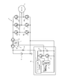
- FIG. 1 is a diagram illustrating an internal configuration of a switch drive circuit according to the first embodiment.
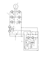
- FIG. 2 is a functional block diagram showing the internal configuration of the motor drive control unit.
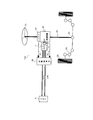
- FIG. 3 is a diagram showing a configuration of the entire power steering apparatus.
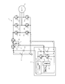
- FIG. 4 is a view corresponding to FIG. 1 showing the second embodiment.
- FIG. 5 is a view corresponding to FIG. 1 showing a third embodiment.
- FIG. 6 is a view corresponding to FIG.
- FIG. 7 is a view corresponding to FIG. 6 when the batteries are connected with reverse polarity.
- FIG. 6 is a view corresponding to FIG. 6 when a switch is configured using a P-channel MOSFET.
- 1 is an inverter circuit
- 3 is a motor
- 4 is a battery (DC power supply)
- 5 is a switch drive circuit
- 6 is an N-channel MOSFET (N-channel semiconductor switching element)
- 10 and 11 are N-channel MOSFETs (semiconductor switching elements)
- Reference numerals 13 and 14 denote protective diodes
- 38 denotes a switch drive circuit
- 39 denotes a current blocking diode
- 41 denotes a switch drive circuit
- 42 and 43 denote current blocking diodes
- 100 denotes a power steering device.
- FIGS. 1 to 3 a first embodiment will be described with reference to FIGS. 1 to 3. Note that the same parts as those in FIG. In FIG. 3 showing the overall configuration of the power steering apparatus 100, one end of the steering shaft 22 is fixed to a steering handle 21 disposed in the vehicle interior, and the rotational force of the rack shaft is driven by a rack and pinion mechanism 23. It is transmitted as a force that changes the direction of the wheel 25 attached to both ends via the connecting mechanism 24.
- the three-phase brushless DC motor 3 for assisting the rotational force is disposed on the steering shaft 22, and the motor 3 and the shaft 22 are connected via a speed reduction mechanism 26.
- the power supply voltage of the battery 4 is supplied to the motor drive control unit 28 via the wires 27a and 27b.
- the motor drive control unit 28 is disposed adjacent to or close to the vicinity of the motor 3, and performs PWM control of energization of the motor 3.
- a battery voltage is supplied to the motor drive control unit 28 as a control power source via the wiring 27, and the signal line 30 of the torque sensor 29 for detecting the torque applied to the steering shaft 22 and the rotational position of the motor 3 are set.
- a signal line 32 of a resolver 31 to be detected is connected.
- FIG. 2 is a functional block diagram showing the internal configuration of the motor drive control unit 28.
- the current detector 33 (for example, a resistance element) is connected between the negative terminal (reference potential point) of the battery 4 and the negative DC bus of the inverter circuit 1, and the current signal obtained by the current detector 33 is The signal is input to the A / D conversion circuit 34.
- the current detection circuit 33 may be a current probe that detects a current by detecting a magnetic field generated by the current.
- the A / D conversion circuit 34 outputs data obtained by A / D converting the input current signal to the MCU 35.
- a steering angle signal from the torque sensor 29 and a steering angle signal from the resolver 31 are given to the input I / F (interface) circuit 36, and the input I / F circuit 36 responds to each input signal.
- a voltage signal is input to the MCU 35.
- the MCU 35 is configured by a microcomputer or the like, generates a gate signal for controlling each FET 2 constituting the inverter circuit 1 according to each input signal, and outputs the gate signal to the bridge gate drive circuit 37.
- the MCU 35 outputs a drive signal to the switch circuit 5 via the switch drive circuit 38.
- the MCU 35 When the power is supplied, the MCU 35 first outputs a shut-off command (OFF) signal to the switch circuit 5, and outputs a closing (ON) signal to the switch circuit 5 when its initialization process is completed. Thereby, the electric power of the battery 4 is supplied to the inverter circuit 1.
- the MCU 35 takes in the steering torque signal and the steering rotation speed, determines whether or not it is necessary to supply the steering assist force (torque) from the motor 3, and if so, based on the steering torque and the steering rotation speed. Thus, the rotation direction of the motor 3 and the steering assist force supplied from the motor 3 are obtained. Then, the MCU 35 generates and outputs a gate drive control signal based on the obtained rotation direction and steering assist force. Further, the MCU 35 outputs a cutoff command signal to the switch circuit 5 when the current value detected by the current detector 33 exceeds the overcurrent value.
- the bridge gate drive circuit 37 includes a booster circuit for generating a gate supply voltage for controlling the FETs 2U to 2W on the upper arm side constituting the inverter circuit 1 to a conductive state, and a plurality of level shift circuits (both shown in FIG. Not shown).
- the gate drive circuit 37 supplies a gate voltage signal to the gate of each FET 2 based on the gate drive control signal output from the MCU 35.
- the MCU 35 monitors the current flowing through the inverter circuit 1 based on the current value signal. When the current flowing through the inverter circuit 1 exceeds a preset allowable current, the MCU 35 stops driving the motor 3 and sends it to the switch circuit 5. Is turned off to cut off the power supply to the inverter circuit 1.
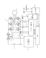
- FIG. 1 is a diagram corresponding to FIG. 6 showing the internal configuration of the switch drive circuit 38.
- the circuit ground is directly connected to the negative DC bus of the inverter circuit 1, but in the switch drive circuit 38 of the present embodiment, the forward diode 39 (current element diode). Is inserted between the two. Thereby, even when the battery 4 is connected with a reverse polarity as shown in FIG. 7, it is possible to prevent an overcurrent from flowing through the circuit via the parasitic diode of the FET 2.
- the switch drive circuit 38 has two N-channel MOSFETs 6a and 6b (N-channel semiconductor switching elements) so as to electrically open and close between the battery 4 and the inverter circuit 1.
- MOSFETs 6a and 6b N-channel semiconductor switching elements
- the reference potential point is shared with the inverter circuit 1 and an open / close control signal is output to the switch circuit 5.
- a half bridge circuit in which two N-channel MOSFETs 10 and 11 (semiconductor switching elements) are connected in series is provided between the power supply generation circuit 9 and the reference potential point. These FETs 10 and 11 are connected in parallel, respectively.
- the switch circuit 5 that can be configured more compactly than a relay for high power, and the power steering device 100 can be downsized. Even when the battery 4 is connected in reverse polarity, the reverse current is prevented from flowing by the parasitic diode of the FET 2 and the protective diode 14 in the switch drive circuit 38 to protect the inverter circuit 1 and the motor 3, and short circuit failure Can be prevented.
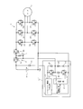
- FIG. 4 shows a second embodiment.
- the same parts as those in the first embodiment are denoted by the same reference numerals and the description thereof is omitted. Hereinafter, different parts will be described.
- a current blocking diode 42 instead of the diode 39, a current blocking diode 42, between the source of the N-channel MOSFET 11 and the circuit ground, and between the anode of the protection diode 14 and the circuit ground, respectively. 43 is inserted.
- the second embodiment configured as described above, the same effect as that of the first embodiment can be obtained.
- FIG. 5 shows a third embodiment, and the differences from the second embodiment will be described.
- the switch drive circuit 41 ′ of the third embodiment includes the current blocking diodes 42 and 43 of the second embodiment between the source of the N-channel MOSFET 10 and the drain of the N-channel MOSFET 11, the anode of the protection diode 13, and the protection diode 14. It is the structure arrange
- a P-channel MOSFET may be used instead of the N-channel MOSFET 10. Further, a P-channel MOSFET may be used for the upper arm of the inverter circuit 1.
- the present invention is not limited to a power steering device, and any device having a switch circuit configured using an N-channel semiconductor switching element between a DC power source and an inverter circuit is applicable.
- the switch drive circuit according to the embodiment of the present invention is configured by connecting two N-channel type semiconductor switching elements in series in the reverse direction in order to electrically open and close between the DC power supply and the inverter circuit. This is useful for opening and closing a switch circuit.
Landscapes
- Engineering & Computer Science (AREA)
- Power Engineering (AREA)
- Inverter Devices (AREA)
- Power Steering Mechanism (AREA)
- Physics & Mathematics (AREA)
- Ceramic Engineering (AREA)
- Condensed Matter Physics & Semiconductors (AREA)
- General Physics & Mathematics (AREA)
- Microelectronics & Electronic Packaging (AREA)
Priority Applications (4)
| Application Number | Priority Date | Filing Date | Title |
|---|---|---|---|
| EP12830399.7A EP2755314B1 (en) | 2011-09-07 | 2012-08-10 | Switch driving circuit, inverter apparatus and power steering apparatus |
| CN201280041766.3A CN103782469B (zh) | 2011-09-07 | 2012-08-10 | 开关驱动电路、逆变器装置以及动力转向装置 |
| KR1020147008758A KR101711711B1 (ko) | 2011-09-07 | 2012-08-10 | 스위치 구동 회로, 인버터 장치 및 파워 스티어링 장치 |
| US14/200,858 US9564485B2 (en) | 2011-09-07 | 2014-03-07 | Switch driving circuit, inverter apparatus and power steering apparatus |
Applications Claiming Priority (2)
| Application Number | Priority Date | Filing Date | Title |
|---|---|---|---|
| JP2011-195051 | 2011-09-07 | ||
| JP2011195051A JP5638488B2 (ja) | 2011-09-07 | 2011-09-07 | スイッチ駆動回路,インバータ装置及びパワーステアリング装置 |
Related Child Applications (1)
| Application Number | Title | Priority Date | Filing Date |
|---|---|---|---|
| US14/200,858 Continuation US9564485B2 (en) | 2011-09-07 | 2014-03-07 | Switch driving circuit, inverter apparatus and power steering apparatus |
Publications (1)
| Publication Number | Publication Date |
|---|---|
| WO2013035491A1 true WO2013035491A1 (ja) | 2013-03-14 |
Family
ID=47831942
Family Applications (1)
| Application Number | Title | Priority Date | Filing Date |
|---|---|---|---|
| PCT/JP2012/070504 Ceased WO2013035491A1 (ja) | 2011-09-07 | 2012-08-10 | スイッチ駆動回路,インバータ装置及びパワーステアリング装置 |
Country Status (6)
| Country | Link |
|---|---|
| US (1) | US9564485B2 (enExample) |
| EP (1) | EP2755314B1 (enExample) |
| JP (1) | JP5638488B2 (enExample) |
| KR (1) | KR101711711B1 (enExample) |
| CN (1) | CN103782469B (enExample) |
| WO (1) | WO2013035491A1 (enExample) |
Families Citing this family (16)
| Publication number | Priority date | Publication date | Assignee | Title |
|---|---|---|---|---|
| JP5638488B2 (ja) * | 2011-09-07 | 2014-12-10 | 株式会社東芝 | スイッチ駆動回路,インバータ装置及びパワーステアリング装置 |
| US9609718B1 (en) | 2014-03-28 | 2017-03-28 | Mitsubishi Electric Corporation | In-vehicle equipment |
| EP3041103A1 (en) * | 2014-12-29 | 2016-07-06 | Rockwell Automation Limited | Circuit protection |
| KR20170028133A (ko) | 2015-09-03 | 2017-03-13 | 주식회사 만도 | 방열 구조가 개선된 인버터 어셈블리 |
| GB2555117B (en) * | 2016-10-18 | 2022-03-02 | Trw Ltd | A motor drive circuit |
| GB2557295B (en) * | 2016-12-05 | 2022-07-20 | Trw Ltd | Control for electric power steering |
| JP6613256B2 (ja) * | 2017-03-13 | 2019-11-27 | ミネベアミツミ株式会社 | 保護回路及び負荷駆動回路 |
| US20180302017A1 (en) * | 2017-04-12 | 2018-10-18 | Power Integrations, Inc. | Current sense circuit for a dc motor inverter |
| JP6903597B2 (ja) * | 2018-01-31 | 2021-07-14 | ミネベアミツミ株式会社 | 負荷駆動回路 |
| KR102502388B1 (ko) * | 2018-06-19 | 2023-02-23 | 에이치엘만도 주식회사 | 차량의 eps 전원 공급 제어 장치 및 방법 |
| FR3083770B1 (fr) * | 2018-07-10 | 2020-06-19 | Jtekt Europe | Procede de controle d’un systeme de direction avec deux motorisations redondantes |
| KR102434048B1 (ko) * | 2018-07-26 | 2022-08-19 | 현대모비스 주식회사 | 전자식 릴레이 장치 |
| DE102020103190A1 (de) | 2019-02-08 | 2020-08-13 | Steering Solutions Ip Holding Corporation | Halbleiter-motordämpfung |
| US20230336106A1 (en) * | 2020-09-18 | 2023-10-19 | Techtronic Cordless Gp | Motor driven appliance and protection method thereof |
| GB2601532B (en) * | 2020-12-03 | 2024-06-12 | Dyson Technology Ltd | Gate driver |
| DE102021125556A1 (de) * | 2021-10-01 | 2023-04-06 | HELLA GmbH & Co. KGaA | Batteriemanagementsystem für einen Batteriespeicher, Anordnung und Verfahren |
Citations (3)
| Publication number | Priority date | Publication date | Assignee | Title |
|---|---|---|---|---|
| JP2004168124A (ja) * | 2002-11-19 | 2004-06-17 | Nissan Motor Co Ltd | ブレーキ制御装置 |
| JP2009274686A (ja) * | 2008-05-19 | 2009-11-26 | Nsk Ltd | 電動パワーステアリング装置 |
| JP2010259245A (ja) * | 2009-04-27 | 2010-11-11 | Yaskawa Electric Corp | 出力フィルタおよび電力変換装置 |
Family Cites Families (12)
| Publication number | Priority date | Publication date | Assignee | Title |
|---|---|---|---|---|
| DE3835662A1 (de) * | 1988-10-20 | 1990-04-26 | Daimler Benz Ag | Vorrichtung zur ansteuerung induktiver verbraucher in einem kraftfahrzeug |
| JP3375502B2 (ja) | 1996-12-12 | 2003-02-10 | 本田技研工業株式会社 | 電動パワーステアリング装置 |
| JP3698550B2 (ja) * | 1998-07-02 | 2005-09-21 | 富士通株式会社 | ブースト回路及びこれを用いた半導体装置 |
| IL134628A0 (en) * | 2000-02-20 | 2001-04-30 | Elisra Electronic Systems Ltd | Electronic circuit breaker |
| FR2851698B1 (fr) * | 2003-02-21 | 2005-08-19 | Valeo Systemes Dessuyage | Circuit de commande d'un moteur electrique a courant continu et systeme d'essuyage utilisant un tel circuit |
| DE102004007991B4 (de) * | 2004-02-18 | 2015-07-30 | Infineon Technologies Ag | Halbleiter-Schaltelement |
| CN200983560Y (zh) * | 2006-09-05 | 2007-11-28 | 任文华 | 一种组合式开关及电源装置 |
| DE102008016589A1 (de) * | 2008-03-31 | 2009-10-01 | Weidmüller Interface GmbH & Co. KG | Schutzvorrichtung |
| JP2010074915A (ja) * | 2008-09-17 | 2010-04-02 | Jtekt Corp | モータ制御装置及び電動パワーステアリング装置 |
| JP5246407B2 (ja) * | 2008-11-04 | 2013-07-24 | 株式会社ジェイテクト | モータ駆動回路及び電動パワーステアリング装置 |
| CN201717802U (zh) * | 2010-07-05 | 2011-01-19 | 常熟开关制造有限公司(原常熟开关厂) | 一种防反接逆变电路 |
| JP5638488B2 (ja) * | 2011-09-07 | 2014-12-10 | 株式会社東芝 | スイッチ駆動回路,インバータ装置及びパワーステアリング装置 |
-
2011
- 2011-09-07 JP JP2011195051A patent/JP5638488B2/ja active Active
-
2012
- 2012-08-10 WO PCT/JP2012/070504 patent/WO2013035491A1/ja not_active Ceased
- 2012-08-10 CN CN201280041766.3A patent/CN103782469B/zh active Active
- 2012-08-10 EP EP12830399.7A patent/EP2755314B1/en active Active
- 2012-08-10 KR KR1020147008758A patent/KR101711711B1/ko active Active
-
2014
- 2014-03-07 US US14/200,858 patent/US9564485B2/en active Active
Patent Citations (3)
| Publication number | Priority date | Publication date | Assignee | Title |
|---|---|---|---|---|
| JP2004168124A (ja) * | 2002-11-19 | 2004-06-17 | Nissan Motor Co Ltd | ブレーキ制御装置 |
| JP2009274686A (ja) * | 2008-05-19 | 2009-11-26 | Nsk Ltd | 電動パワーステアリング装置 |
| JP2010259245A (ja) * | 2009-04-27 | 2010-11-11 | Yaskawa Electric Corp | 出力フィルタおよび電力変換装置 |
Also Published As
| Publication number | Publication date |
|---|---|
| EP2755314A1 (en) | 2014-07-16 |
| US9564485B2 (en) | 2017-02-07 |
| CN103782469B (zh) | 2016-09-21 |
| EP2755314B1 (en) | 2020-10-21 |
| JP5638488B2 (ja) | 2014-12-10 |
| EP2755314A4 (en) | 2016-06-01 |
| KR20140057380A (ko) | 2014-05-12 |
| KR101711711B1 (ko) | 2017-03-02 |
| JP2013059167A (ja) | 2013-03-28 |
| CN103782469A (zh) | 2014-05-07 |
| US20140184107A1 (en) | 2014-07-03 |
Similar Documents
| Publication | Publication Date | Title |
|---|---|---|
| JP5638488B2 (ja) | スイッチ駆動回路,インバータ装置及びパワーステアリング装置 | |
| JP5743934B2 (ja) | インバータ装置及びパワーステアリング装置 | |
| JP5532065B2 (ja) | 電動機駆動装置 | |
| CN101883706B (zh) | 电动动力转向装置 | |
| CN103359159B (zh) | 电机驱动装置 | |
| KR101704112B1 (ko) | 모터 구동 장치 | |
| JP2011244611A (ja) | モータ駆動装置 | |
| JP2015171305A (ja) | 電源供給回路 | |
| JP2015165745A (ja) | 電源供給回路 | |
| JP6268140B2 (ja) | 電動モータ駆動回路 | |
| US10404202B2 (en) | Electronic control device and control method thereof | |
| JP7226533B2 (ja) | 電気機器 | |
| KR102313672B1 (ko) | 전동식 파워 스티어링 시스템의 모터 구동 회로 | |
| JP5660996B2 (ja) | 電動機制御装置 | |
| US9694695B2 (en) | Power source system | |
| WO2023026943A1 (ja) | 電力供給装置 | |
| JP5458954B2 (ja) | 電動パワーステアリング装置 | |
| WO2024057878A1 (ja) | モータ制御装置及び電動操舵装置 |
Legal Events
| Date | Code | Title | Description |
|---|---|---|---|
| 121 | Ep: the epo has been informed by wipo that ep was designated in this application |
Ref document number: 12830399 Country of ref document: EP Kind code of ref document: A1 |
|
| NENP | Non-entry into the national phase |
Ref country code: DE |
|
| WWE | Wipo information: entry into national phase |
Ref document number: 2012830399 Country of ref document: EP |
|
| ENP | Entry into the national phase |
Ref document number: 20147008758 Country of ref document: KR Kind code of ref document: A |