WO2013021774A1 - コネクタ - Google Patents
コネクタ Download PDFInfo
- Publication number
- WO2013021774A1 WO2013021774A1 PCT/JP2012/067678 JP2012067678W WO2013021774A1 WO 2013021774 A1 WO2013021774 A1 WO 2013021774A1 JP 2012067678 W JP2012067678 W JP 2012067678W WO 2013021774 A1 WO2013021774 A1 WO 2013021774A1
- Authority
- WO
- WIPO (PCT)
- Prior art keywords
- connector
- metal plating
- plating pattern
- peripheral edge
- front surface
- Prior art date
- Legal status (The legal status is an assumption and is not a legal conclusion. Google has not performed a legal analysis and makes no representation as to the accuracy of the status listed.)
- Ceased
Links
Images






Classifications
-
- H—ELECTRICITY
- H01—ELECTRIC ELEMENTS
- H01R—ELECTRICALLY-CONDUCTIVE CONNECTIONS; STRUCTURAL ASSOCIATIONS OF A PLURALITY OF MUTUALLY-INSULATED ELECTRICAL CONNECTING ELEMENTS; COUPLING DEVICES; CURRENT COLLECTORS
- H01R13/00—Details of coupling devices of the kinds covered by groups H01R12/70 or H01R24/00 - H01R33/00
- H01R13/46—Bases; Cases
- H01R13/52—Dustproof, splashproof, drip-proof, waterproof, or flameproof cases
- H01R13/521—Sealing between contact members and housing, e.g. sealing insert
-
- H—ELECTRICITY
- H01—ELECTRIC ELEMENTS
- H01R—ELECTRICALLY-CONDUCTIVE CONNECTIONS; STRUCTURAL ASSOCIATIONS OF A PLURALITY OF MUTUALLY-INSULATED ELECTRICAL CONNECTING ELEMENTS; COUPLING DEVICES; CURRENT COLLECTORS
- H01R13/00—Details of coupling devices of the kinds covered by groups H01R12/70 or H01R24/00 - H01R33/00
- H01R13/40—Securing contact members in or to a base or case; Insulating of contact members
-
- H—ELECTRICITY
- H01—ELECTRIC ELEMENTS
- H01R—ELECTRICALLY-CONDUCTIVE CONNECTIONS; STRUCTURAL ASSOCIATIONS OF A PLURALITY OF MUTUALLY-INSULATED ELECTRICAL CONNECTING ELEMENTS; COUPLING DEVICES; CURRENT COLLECTORS
- H01R13/00—Details of coupling devices of the kinds covered by groups H01R12/70 or H01R24/00 - H01R33/00
- H01R13/73—Means for mounting coupling parts to apparatus or structures, e.g. to a wall
- H01R13/74—Means for mounting coupling parts in openings of a panel
-
- H—ELECTRICITY
- H01—ELECTRIC ELEMENTS
- H01R—ELECTRICALLY-CONDUCTIVE CONNECTIONS; STRUCTURAL ASSOCIATIONS OF A PLURALITY OF MUTUALLY-INSULATED ELECTRICAL CONNECTING ELEMENTS; COUPLING DEVICES; CURRENT COLLECTORS
- H01R43/00—Apparatus or processes specially adapted for manufacturing, assembling, maintaining, or repairing of line connectors or current collectors or for joining electric conductors
- H01R43/20—Apparatus or processes specially adapted for manufacturing, assembling, maintaining, or repairing of line connectors or current collectors or for joining electric conductors for assembling or disassembling contact members with insulating base, case or sleeve
Definitions
- the present invention relates to a connector responsible for electrical connection in an airtight device.
- Patent Document 1 discloses a connector that performs electrical connection between the inside and outside of a partition of a vacuum chamber in which the inside of the partition is depressurized.
- the connector has a ceramic substrate that closes the through hole of the adapter.
- a brazing region is formed on the entire circumference of one surface of the ceramic substrate.
- Patent Document 2 discloses a sensor that holds a vacuum between an anode substrate and a cathode substrate. A solder adhesion layer is formed on the side surface of the anode substrate.
- Patent Document 3 discloses an integrated circuit board.
- a wiring pattern is formed on the side surface in addition to the periphery of the front and back surfaces.
- the connector arranged at a position covering the hole of the partition wall hermetically closes the hole by brazing (typically soldering) the edge of the surface facing the partition wall to the partition wall over the entire circumference.
- brazing typically soldering
- Such a connector mounting structure is required to further improve the airtightness so as to be applicable to an environment in which the inside of the partition wall is pressurized or decompressed, for example.
- An object of the present invention is to provide a connector capable of solving the above problems and further improving the airtightness.
- the connector of the present invention that achieves the above object is attached to a position covering the hole of the partition wall having a hole to close the hole, and is responsible for electrical connection between the inside and the outside of the partition wall through the hole.
- a connector It is made of an insulating material, and has a surface facing the partition, a back surface with respect to the surface, and a side surface that connects the peripheral edge of the surface and the peripheral edge of the back surface.
- a plate-like insulating substrate having a bulging portion swelled outward compared to the peripheral edge of the front surface in a region away from the back surface side, A first metal plating pattern that continuously circulates in a region adjacent to the periphery of the surface of the surface; A second metal plating pattern that continuously circulates in a region adjacent to the periphery of the surface of the side surface; It is made of a conductive material, and includes an electrical connection portion exposed on both the front surface and the back surface and electrically connected from the front surface to the back surface.
- the connector of the present invention is attached to a position covering the hole of the partition wall, and the partition wall hole is hermetically sealed by soldering between the first metal plating pattern provided on the periphery of the surface and the partition wall. Close up. In soldering, the melted solder spreads on the second metal plating pattern that circulates around the side surface to form a solder fillet.
- the connector of the present invention has a bulge on the side surface.
- the connector of the present invention is a router or the like. First, an insulating plate is continuously carved along the shape of the side surface of the connector, leaving a part of the thickness. It is manufactured by cutting. A second metal plating pattern is formed on the side portion formed by carving by metal plating. At the time of cutting, the cutting tool does not contact the second metal plating pattern by cutting so as to form a bulging portion. Therefore, the connector of the present invention is manufactured so that the second metal plating pattern has a smooth shape.
- the solder fillet does not concentrate on a part of the entire circumference of the second metal plating pattern or is deficient in a part thereof. Over a uniform thickness. Therefore, the airtightness between the connector and the partition is further improved by the solder fillet that spreads uniformly around the entire circumference of the side surface.
- the bulge portion protrudes laterally from the second metal plating pattern at a position on the side surface away from the peripheral edge of the front surface to the back surface side. It is preferable that
- Such a connector can be easily cut by a processing machine such as a router.
- the bulging portion is a protrusion extending around the side surface.
- This connector is manufactured by carving a groove with a certain depth along the shape of the side of the connector on an insulating plate and cutting a part of the groove after metal plating. By carving a groove having a certain depth, it is easy to form a smooth surface of the second metal plating pattern.
- a region of the side surface adjacent to the peripheral edge of the surface is formed on a slope extending outward from the front surface side toward the back surface side, and the bulge portion is formed on the side surface. It may consist of a region connecting the slope and the peripheral edge of the back surface.
- a region of the side surface of the insulating substrate on which the second metal plating pattern is formed is formed with an outwardly convex curved surface allowing a part to be a flat surface. Preferably it is.
- solder fillet spreads more uniformly than in the case where, for example, corners or recesses are provided in the region where the second metal plating pattern is formed.
- the insulating substrate has a groove narrower than the first metal plating pattern, which extends in a circular shape around the periphery of the surface, and the first metal plating pattern is It is preferable that the groove is formed so as to surround the groove.
- the solder is filled between the first metal plating pattern and the partition wall. At this time, when the solder enters the groove extending in a circular shape, a thick portion of the solder is formed in a circular shape. Therefore, the airtightness between the first metal plating pattern and the partition is further improved.
- a connector capable of further improving the airtightness is realized.
- FIG. 2 is a cross-sectional view showing a cross section of the connector shown in FIG. It is a top view which shows the cutting process of the connector shown in FIG. 1 and FIG. It is sectional drawing which shows the cross section of the board
- FIG. 13 It is a perspective view which shows the connector which is 2nd Embodiment of this invention. It is a top view which shows a cutting process among the manufacturing processes of the connector shown in FIG. It is sectional drawing of the board
- FIG. 1 is a perspective view showing a connector according to a first embodiment of the present invention.
- the connector 1 shown in FIG. 1 is a flat part.
- the connector 1 is attached to a position that covers a hole of a partition wall, which will be described later, and closes the hole, and performs electrical connection between the inside and the outside of the partition wall through the hole.
- FIG. 1 shows a front surface (surface) 11a of the connector 1 facing the partition wall.
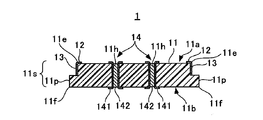
- FIG. 2 is a cross-sectional view showing a cross section taken along line 2-2 of the connector shown in FIG. The connector 1 will be described with reference to FIGS. 1 and 2.
- the connector 1 includes an insulating substrate 11, a first metal plating pattern 12, a second metal plating pattern 13, and an electrical connection portion 14.
- the insulating substrate 11 is a rounded rectangular shape made of an insulating material, that is, an oval plate shape.
- the material of the insulating substrate 11 is, for example, glass epoxy or ceramic.
- the insulating substrate 11 has a surface 11a facing the partition, a back surface 11b opposite to the surface, and a side surface 11s.
- the side surface 11s makes a round by connecting the peripheral edge 11e of the front surface 11a and the peripheral edge f of the back surface 11b.
- the side surface 11s of the insulating substrate 11 is provided with a bulging portion 11p that swells outward as compared to the peripheral edge 11e of the front surface 11a in a region away from the peripheral edge 11e of the front surface 11a toward the back surface 11b.
- the bulging portion 11p in the present embodiment is a ridge extending around the side surface 11s. More specifically, the bulging portion 11p is a portion that is enlarged in a flange shape on the back surface 11b side of the side
- the first metal plating pattern 12 and the second metal plating pattern 13 continuously spread on the surface 11a and the side surface 11s of the insulating substrate 11.
- the first metal plating pattern 12 continuously circulates in a strip shape in a region adjacent to the peripheral edge 11 e of the surface 11 a of the insulating substrate 11. That is, the first metal plating pattern 12 makes one round along the peripheral edge 11e of the surface 11a.
- the second metal plating pattern 13 continuously circulates in a strip shape in a region adjacent to the peripheral edge 11f of the surface 11a of the side surface 11s of the insulating substrate 11. In other words, the second metal plating pattern 13 continues from the first metal plating pattern 12 and makes one round on the side surface 11s without interruption.
- the surface on which the second metal plating pattern 13 is formed is substantially perpendicular to the surface 11a on which the first metal plating pattern 12 is formed.
- the bulging portion 11 p of the insulating substrate 11 protrudes to the side of the second metal plating pattern 13.
- the region of the side surface 11s where the second metal plating pattern 13 is formed and the bulging portion 11p are both formed of an outwardly convex curved surface and a flat surface.
- the connector 1 shown in the figure is a 28-pole connector, and 28 electrical connection portions 14 are arranged on the insulating substrate 11 of the connector 1.
- Each electrical connection portion 14 is formed of a conductive material.
- Each electrical connection part 14 is exposed to both the front surface 11a and the back surface 11b, and is electrically connected from the front surface 11a to the back surface 11b. More specifically, in the electrical connection portion 14 of the present embodiment, the through hole 11h penetrating from the front surface 11a to the back surface 11b of the insulating substrate 11 is hermetically closed by the metal plating film 141 and the sealing material 142.
- the inner wall surface of the through hole 11 h is covered with a metal plating film 141, and the sealing material 142 is filled in the through hole 11 h covered with the metal plating film 141.
- the material of the metal plating film 141 is, for example, copper, and the sealing material 142 is solder mainly composed of tin.
- metals other than copper can be used as the material of the metal plating film 141.
- an alloy or resin mainly composed of aluminum or silver can be used as the material of the sealing material 142.
- the sealing material 142 is in close contact with the metal plating film 141, even if a pressure difference occurs between the front surface 11 a and the back surface 11 b of the insulating substrate 11, there is no gap that allows gas to escape from the front surface 11 a to the back surface 11 b.
- FIG. 3 to 7 are diagrams for explaining a manufacturing process of the connector shown in FIG. 1 and FIG.
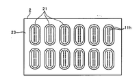
- FIG. 3 is a plan view showing a cutting process.
- an insulating substrate 2 is first prepared.
- the material of the substrate 2 is, for example, glass epoxy or ceramic.
- a groove 21 along the shape of the connector 1 is carved on the substrate 2 as shown in FIG.
- a plurality of connectors 1 can be obtained from a single substrate 2.
- a through hole 11h is also formed.
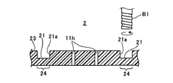
- FIG. 4 is a cross-sectional view showing a cross section of the substrate shown in FIG. FIG. 4 shows a portion corresponding to one connector.
- the groove 21 is formed, for example, by scraping the substrate 2 with a router bit B1 which is a rotating rod-shaped excavating blade provided in a router processing apparatus (not shown).
- the router bit B1 continuously moves over the entire circumference along the shape of the side surface 11s (see FIG. 1) of the connector 1 while cutting the substrate 2 to form a recess shallower than the thickness of the substrate 2. In this way, a bottomed continuous groove 21 is formed.
- the side surface 21a of the groove 21 is formed by the continuous advancement of the router bit B1, it is smooth over the entire circumference.
- a portion to be a connector and a frame 23 which is the remaining portion are formed on the substrate 2.
- the portion that is in contact with the bottom of the groove 21 and is thinner than the thickness of the substrate 2 functions as a carrier 24 that connects the portion to be a connector and the frame 23.
- a portion to be a plurality of connectors is handled in a state of being integrated with the frame 23 via the carrier 24. For this reason, it is easier to handle than the case where the parts to be the connectors are individually separated and can be applied to a mass production process.
- the substrate 2 that has undergone the cutting process is then subjected to metal plating.
- the substrate In the plating process, the substrate is immersed in a plating solution in a state where a resist (not shown) is applied to a portion that does not require plating.
- the plating material is, for example, copper. However, metals other than copper can be used for plating. After removing the substrate 2 from the plating solution, the metal plating pattern is formed on the target portion by removing the resist.
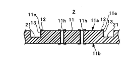
- FIG. 5 is a cross-sectional view showing a state after the plating process.
- the first metal plating pattern 12 continuously circulates in a band shape in a region adjacent to the peripheral edge 11e of the surface 11a in the portion to be the insulating substrate 11 of the connector.
- the second metal plating pattern 13 follows the first metal plating pattern 12.
- the second metal plating pattern 13 continuously circulates in a strip shape in a region adjacent to the peripheral edge 11e of the surface 11a in the portion that becomes the side surface 11s (see FIG. 2) of the insulating substrate 11.
- the second metal plating pattern 13 is formed on the side surface 21a (see FIG. 4) of the groove 21 formed in the cutting process.
- the second metal plating pattern 13 formed on the side surface 21a is also smooth over the entire circumference.
- the metal plating pattern covers the inner wall surface of the through hole 11h and spreads on the front surface 11a and the back surface 11b of the insulating substrate 11.
- This metal plating pattern becomes the metal plating film 141 in the electrical connection portion 14 (see FIG. 2).
- the inside of the through hole 11h covered with the metal plating film 141 is filled with a sealing material made of a conductive material. Thereafter, the sealing material is welded to the metal plating film 141 by heat treatment.
- the sealing material is, for example, solder containing tin as a main component. However, an alloy mainly composed of aluminum or silver can also be used as the sealing material. Further, the sealing material is not limited to a conductive material, and may be, for example, an airtight resin such as a trade name “Torr Seal” (registered trademark), or other materials that ensure airtightness. After cutting and filling, cutting is performed.
- FIG. 6 and 7 are diagrams for explaining the cutting process. 6 is a plan view, and FIG. 7 is a cross-sectional view.
- the frame 23 is removed by cutting the carrier 24.
- the carrier 24 that is, the portion corresponding to the bottom of the groove 21 carved in the cutting process, is larger than the bulging portion 11 p swelled outward as compared with the peripheral edge 11 e of the surface 11 a, that is, the second metal plating pattern 13. It cut
- the router bit B2 having a diameter smaller than that of the router bit B1 (see FIG. 4) used in the cutting process cuts the path near the outer periphery of the groove 21 over one round.
- the cutting method is not limited to a method using a small-sized router bit.
- a router bit having the same diameter as the router bit B1 (see FIG. 4) used in the cutting process is disposed outside the groove 21 so as to overlap the groove 21. It is also possible to employ a method of cutting off the shifted path. Further, the cutting method is not limited to the method using a router bit, and for example, a pressing method in which a thin blade formed into a shape to be cut is pushed can be employed.
- the frame 23 is removed by the cutting process, and the connector 1 shown in FIGS. 1 and 2 is completed.
- cutting is performed so as to form a bulging portion 11p that is swollen more than the second metal plating pattern 13, so that a cutting tool such as a router bit B1 or a thin blade does not contact the second metal plating pattern 13. . Therefore, it is possible to avoid the second metal plating pattern 13 from being uneven or scratched by the cutting tool. Therefore, the smoothness of the second metal plating pattern 13 is maintained.
- FIG. 8 is a schematic configuration diagram showing an application example of the connector 1 shown in FIGS. 1 and 2.
- the apparatus 3 shown in FIG. 8 is a chamber apparatus that operates in an atmosphere in which pressure and composition are adjusted. More specifically, the device 3 includes a partition wall 31, an internal circuit board 32, an external circuit board 33, and the connector 1 shown in FIGS. 1 and 2. In FIG. 8, the connector 1 is disposed with the surface 11a shown in FIG. 1 facing down.
- the partition wall 31 is a container that partitions an external space and an internal space.
- An internal circuit board 32 is disposed inside the partition wall 31. On the internal circuit board 32, electronic components and mechanism devices that operate in a reduced or pressurized atmosphere are mounted.
- the partition wall 31 is provided with a wiring hole 31h for electrical wiring.
- the connector 1 is larger than the wiring hole 31h and is attached at a position covering the wiring hole 31h, thereby closing the wiring hole 31h. More specifically, the insulating substrate 11 (see FIG. 1) of the connector 1 closes the wiring hole 31h.
- the connector 1 is responsible for electrical connection between the inside and the outside of the partition wall 31 via the wiring hole 31h. Solder as a sealing material is filled between the insulating substrate 11 and the partition wall 31 of the connector 1.
- the external circuit board 33 is disposed outside the partition wall 31 and supplies power to the internal circuit board 32 and controls the internal circuit board 32.
- the internal circuit board 32 and the external circuit board 33 are counterpart parts to which the connector 1 is connected.
- the internal circuit board 32 and the external circuit board 33 have contacts 321 and 331 that contact the connector 1, respectively.
- the internal circuit board 32 and the external circuit board 33 are electrically connected to each other via the connector 1.
- the partition wall 31 becomes airtight when the connector 1 is attached. By discharging or injecting air or gas from the inlet / outlet 312, the pressure inside the partition wall 31 is reduced or increased from the outside. Electronic components and mechanism devices of the internal circuit board 32 operate under this pressure.
- FIG. 9 is an enlarged cross-sectional view showing the vicinity of the connector of the apparatus shown in FIG. In FIG. 9, parts other than the connector 1 and the partition wall 31 are not shown.
- the connector 1 is fixed to the partition wall 31 with solder S.
- solder preform solder
- solder form solder
- the connector 1 is placed on the solder so that the first metal plating pattern 12 is in contact with the solder.
- the solder is heated.
- the solder is melted by heating and is welded to both the partition wall 31 and the first metal plating pattern 12.
- the melted solder spreads on the second metal plating pattern 13 due to surface tension. For this reason, a solder fillet F extending from the second metal plating pattern 13 to the bottom is formed between the second metal plating pattern 13 and the partition wall 31.
- the second metal plating pattern has scratches or has discontinuous corners in the circumferential direction of the side surface, the molten solder collects in the uneven portions due to the scratches and corners, and the distribution of the solder becomes uneven. As a result, the sealing is weakened at the portion where the solder is taken away. That is, the second metal plating pattern may reduce the airtightness.
- the connector 1 of the present embodiment has a bulging portion 11p that bulges outward than the peripheral edge 11e of the surface 11a on the side surface 11s, that is, the bulging portion 11 that bulges more than the second metal plating pattern 13, As described above, the second metal plating pattern 13 can be manufactured without scratching. Thereby, when this connector 1 is solder-connected to the partition wall 31, the thickness of the solder fillet formed between the second metal plating pattern 13 and the partition wall 31 is made uniform in the circumferential direction of the side surface 11s. be able to. For this reason, the situation where sealing becomes partially thin is prevented. Therefore, the connector 1 of this embodiment can further improve the airtightness of the partition wall to be attached.
- the connector 1 of the present embodiment has the second metal plating pattern 13 on the side surface 11s, a solder fillet is formed on the side surface 11s. For this reason, the state of sealing with solder is easy to visually recognize.
- the insulating substrate is cut out without a protruding portion and the cut is smoothed with a file and then plated. It is done.
- the connector 1 of the present embodiment can be put into a process such as plating while the part to be a connector is connected to the frame 23 in the manufacturing process.
- a plurality of parts to be the connectors can be collected and connected to the frame 23 for processing. Therefore, a connector having a second metal plating pattern having a smooth shape can be manufactured by a process capable of mass production.
- FIG. 10 is a perspective view showing a connector according to the second embodiment of the present invention.
- the connector 4 shown in FIG. 10 has a protrusion protruding in the four directions outward from the side surface 11s as a bulging portion 41p bulging outward as compared with the peripheral edge 11e of the surface 11a.
- the swelling part 41p of the connector 4 of this embodiment does not circulate on the side surface 11s.
- FIG. 11 is a plan view showing a cutting process in the manufacturing process of the connector shown in FIG.
- the groove 51 along the shape of the connector is carved in the insulating substrate 5 as in the case of the first embodiment.
- the penetrating portion 512 excluding the carrier portion 511 extending in all directions from the connector portion penetrates the front and back surfaces of the substrate 5.
- the carrier part 511 it is a groove
- Such a shape of the groove 51 is formed, for example, by changing the cutting depth during the movement of the router bit.
- FIG. 12 is a cross-sectional view of the substrate shown in FIG. FIG. 12 shows a cross section passing through the carrier portion 511.
- the substrate 5 shown in FIG. 11 undergoes a plating process and the like, and then the carrier portion 511 is cut.
- the cutting process of the carrier portion 511 as shown in FIG. 10, a bulging portion 41p that bulges outward compared to the peripheral edge 11e of the surface 11a, that is, a bulging portion 41p that protrudes from the second metal plating pattern 13 is formed.
- the carrier part 511 is cut so as to be formed. More specifically, the position of the arrow D shown in FIG. 12 is cut.
- the cutting method is the same as in the first embodiment.
- the connector 4 of the present embodiment has a bulging portion 41p that bulges outward compared to the peripheral edge 11e of the surface 11a, that is, a bulge that protrudes beyond the second metal plating pattern 13. It has a portion 41p. For this reason, a cutting tool does not contact the 2nd metal plating pattern 13 at a cutting process. Therefore, the smoothness of the second metal plating pattern 13 is maintained. Therefore, the connector 4 of this embodiment can also improve the airtightness of the mounting structure by solder connection.
- FIG. 13 is a perspective view showing a connector according to a third embodiment of the present invention.
- the connector 6 shown in FIG. 13 is provided with a groove 613 extending in a circular shape on the surface 61 a of the insulating substrate 61.
- the groove 613 is narrower than the first metal plating pattern 62 and extends around the periphery of the surface 61a.
- the first metal plating pattern 62 of the connector 6 is formed in a circular shape so as to cover the groove 613. More specifically, the groove 613 is disposed in the vicinity of the center of the strip-shaped first metal plating pattern 62.
- FIG. 14 is a cross-sectional view showing a state in which the connector shown in FIG. 13 is attached to the partition wall.
- the connector 6 of the present embodiment is fixed to the partition wall 31 with solder S as in the case of the first embodiment.
- the solder S enters the groove 613.
- a thick portion of the solder S is formed in a circular shape between the first metal plating pattern 62 and the partition wall 31. Therefore, the airtightness between the first metal plating pattern 62 and the partition wall 31 is further improved.
- the connector 6 of the present embodiment is provided with the groove 613 along the first metal plating pattern 62, it is easy to position the preform solder when it is attached to the partition wall 31.
- FIG. 15 is a perspective view showing a connector according to a fourth embodiment of the present invention.
- a region of the side surface 71 s adjacent to the peripheral edge 11 e of the front surface 11 a, that is, a region provided with the second metal plating pattern 73 is a slope that spreads outward as it approaches the back surface 11 b side from the front surface 11 a side. Is formed.
- the slope provided with the second metal plating pattern 73 forms an obtuse angle with the surface 11a.
- the swollen portion 71p is composed of a region connecting the slope of the side surface 71s where the second metal plating pattern 73 is provided and the peripheral edge 11f of the back surface 11b.
- FIG. 16 is a plan view showing a cutting step in the manufacturing process of the connector shown in FIG.
- a groove 721 having a V-shaped cross section is carved in the cutting process, and the wall surface of the groove is subjected to metal plating.
- the second metal plating pattern 73 is formed on a slope that spreads outward as it approaches the back surface 11b side from the front surface 11a side.
- the cutting step the position on the inner side from the bottom of the groove 721, that is, the position of the portion that becomes the connector 7 is cut. More specifically, the position of the arrow E shown in FIG. 16 is cut. As a result, a swollen portion 71p shown in FIG. 15 is formed.
- the cutting tool does not contact the second metal plating pattern 73 in the cutting process. Therefore, the smoothness of the second metal plating pattern 73 is maintained. Therefore, the connector 7 of this embodiment can also improve the airtightness of the mounting structure by solder connection.
- a rounded rectangular insulating substrate is shown as an example of the insulating substrate according to the present invention.
- the present invention is not limited to this, and the insulating substrate may have another shape such as an ellipse or a circle.
- the insulating substrate may have a corner on the side surface or a recess.
- the region where the second metal plating pattern is formed is an outwardly convex curved surface that allows a part to be a flat surface, the uniformity of the thickness of the solder fillet is higher.
- the first metal plating pattern in the above-described embodiment is a band shape having a constant thickness.
- the present invention is not limited to this, and the thickness of the first metal plating pattern may be partially different, for example.
- electrical connection portions 14 in the above-described embodiment are provided.
- the present invention is not limited to this, and the number of electrical connection portions may be other than 28.
- the insulating substrate of the connector is not limited to a single layer substrate, and may be a multilayer substrate in which the electrical connection portion does not penetrate the front and back surfaces of the substrate in a straight line.
- the techniques of the above-described embodiments can be combined with each other.
- the groove 613 provided in the connector 6 of the third embodiment may be provided in other embodiments.
Landscapes
- Engineering & Computer Science (AREA)
- Manufacturing & Machinery (AREA)
- Coupling Device And Connection With Printed Circuit (AREA)
- Connections Arranged To Contact A Plurality Of Conductors (AREA)
- Connector Housings Or Holding Contact Members (AREA)
Abstract
気密性の向上が可能なコネクタを提供する。コネクタ(1)は、穴を有する隔壁に取り付けられる。コネクタ(1)は、絶縁基板(11)と、第1の金属メッキパターン(12)と、第2の金属メッキパターン(13)と、電気接続部(14)とを備える。絶縁基板(11)は、絶縁性の材料からなる板状である。絶縁基板(11)は、隔壁に向く表面(11a)と、表面に対する裏面(11b)と、該表面の周縁と該裏面の周縁とを繋いで一周する側面(11s)とを有する。側面(11s)の、表面(11a)の周縁(11e)から裏面(11b)側に離れた領域には、表面(11a)の周縁(11e)と比べ外方に膨らんだ膨み部(11p)を有する。第1の金属メッキパターン(12)は、表面(11a)の周縁(11e)に隣接した領域を帯状に周回する。第2の金属メッキパターン(13)は、側面(11s)の、表面(11a)の周縁(11e)に隣接した領域を帯状に周回する。電気接続部(14)は表面(11a)から裏面(11b)まで電気的に繋がっている。
Description
本発明は、気密性を有する装置における電気接続を担うコネクタに関する。
このようなコネクタとして、例えば特許文献1には、隔壁内部が減圧される真空チャンバの隔壁内と隔壁外との間の電気接続を担うコネクタが示されている。コネクタは、アダプタの貫通孔を塞ぐセラミック基板を有する。セラミック基板の1つの面の全周には、ロウ付け領域が形成されている。
また、特許文献2には、アノード基板とカソード基板の間を真空に保持するセンサが示されている。アノード基板の側面にはハンダ密着層が形成されている。
また、特許文献3には集積回路基板が示されている。この集積回路基板は、表裏面の周に加えて側面にも配線パターンが形成されている。
隔壁の穴を覆う位置に配置されるコネクタは、隔壁に対向する面の縁が、全周に亘って隔壁にろう付け(典型的には半田付け)されることで、穴を気密に塞ぐ。このようなコネクタの取付構造には、例えば隔壁内部が加減圧される環境にも適用可能なように、気密性をより向上することが求められている。
本発明は上記問題点を解決し、気密性をより向上することが可能なコネクタを提供することを目的とするものである。
上記目的を達成する本発明のコネクタは、穴を有する隔壁の穴に被さる位置に取り付けられてこの穴を塞ぐとともに、この穴を介してこの隔壁の内と外との間の電気的接続を担うコネクタであって、
絶縁性の材料からなり、上記隔壁に向く表面と、この表面に対する裏面と、この表面の周縁とこの裏面の周縁とを繋いで一周する側面とを有し、この側面の、この表面の周縁からこの裏面側に離れた領域に、この表面の周縁と比べ外方に膨らんだ膨み部を有する板状の絶縁基板と、
上記表面の、この表面の周縁に隣接した領域を連続的に周回する第1の金属メッキパターンと、
上記側面の、上記表面の周縁に隣接した領域を連続的に周回する第2の金属メッキパターンと、
導電性の材料からなり、上記表面と上記裏面との双方に露出しこの表面からこの裏面まで電気的に繋がった電気接続部とを備えたことを特徴とする。
絶縁性の材料からなり、上記隔壁に向く表面と、この表面に対する裏面と、この表面の周縁とこの裏面の周縁とを繋いで一周する側面とを有し、この側面の、この表面の周縁からこの裏面側に離れた領域に、この表面の周縁と比べ外方に膨らんだ膨み部を有する板状の絶縁基板と、
上記表面の、この表面の周縁に隣接した領域を連続的に周回する第1の金属メッキパターンと、
上記側面の、上記表面の周縁に隣接した領域を連続的に周回する第2の金属メッキパターンと、
導電性の材料からなり、上記表面と上記裏面との双方に露出しこの表面からこの裏面まで電気的に繋がった電気接続部とを備えたことを特徴とする。
本発明のコネクタは、隔壁の穴に被さる位置に取り付けられ、表面の周縁に周回状に設けられた第1の金属メッキパターンと隔壁との間が半田付けされることで、隔壁の穴を気密に塞ぐ。半田付けにおいて、溶融した半田は、側面を周回した第2の金属メッキパターン上に広がり、半田フィレットを形成することとなる。
本発明のコネクタは、側面に膨み部を有する。本発明のコネクタは、まず、ルータ等で、絶縁性の板材を、一部の厚みを残してコネクタの側面の形状に沿って連続して彫り進み、金属メッキ処理をした後に、彫り残しの部分を切断することで製造される。彫られて形成された側面部分に、金属メッキ処理によって、第2の金属メッキパターンが形成される。切断の際、膨み部を形成するように切断することで、切断工具が第2の金属メッキパターンに接触しない。したがって、本発明のコネクタは、第2の金属メッキパターンが滑らかな形状となるように製造される。このため、本発明のコネクタが隔壁に半田付けされる際には、半田フィレットが、第2の金属メッキパターンの全周のうち一部に集中したり一部で欠乏することがなく、全周に亘り均一の厚みに広がる。したがって、コネクタと隔壁との気密性は、側面の全周に均一に広がる半田フィレットによってさらに向上する。
ここで、上記本発明のコネクタにおいて、上記膨み部が、上記側面の、上記表面の周縁から上記裏面側に離れた位置に、上記第2の金属めっきパターンよりも側方に突出した突出部であることが好ましい。
このようなコネクタは、ルータ等の加工機械による切削加工が容易である。
また、上記本発明のコネクタにおいて、上記膨み部が、側面上を周回して延びた突条であることが好ましい。
このコネクタは、絶縁性の板材にコネクタ側面の形状に沿った一定の深さの溝を彫り、金属メッキ処理の後に、溝の一部を切断することで製造される。一定の深さの溝を彫ることで、第2の金属メッキパターンの滑らかな面の形成が容易である。
また、上記本発明のコネクタにおいて、上記側面の、上記表面の周縁に隣接した領域が、この表面側からこの裏面側に向かって外方に広がる斜面に形成され、上記膨み部が、この側面の、この斜面とこの裏面の周縁とを繋ぐ領域からなるものであってもよい。
また、上記本発明のコネクタにおいて、上記絶縁基板の側面の、上記第2の金属メッキパターンが形成された領域が、一部が平面であることを許容した外向きに凸の曲面で形成されていることが好ましい。
この場合には、第2の金属メッキパターンが形成された領域に、例えば角や凹部が設けられた場合に比べ、半田フィレットがより均一に広がる。
また、上記本発明のコネクタにおいて、上記絶縁基板が、上記表面の周縁に周回状に延びた、上記第1の金属メッキパターンよりも幅細の溝を有し、この第1の金属メッキパターンがこの溝を覆って周回状に形成されていることが好ましい。
第1の金属メッキパターンと隔壁の間には半田が充填される。このとき、半田が周回状に延びた溝に入り込むことで、半田の厚い部分が周回状に形成されることとなる。したがって、第1の金属メッキパターンと隔壁の間の気密性がさらに向上する。
以上説明したように、本発明によれば、気密性をより向上することが可能なコネクタが実現する。
以下図面を参照して本発明の実施の形態を説明する。
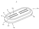
図1は、本発明の第1実施形態であるコネクタを示す斜視図である。
図1に示すコネクタ1は平板状の部品である。コネクタ1は、後に説明する隔壁の穴に被さる位置に取り付けられ、穴を塞ぐとともに、穴を介して隔壁の内と外との間の電気的接続を担う。図1には、コネクタ1の、隔壁に向く表の面(表面)11aが示されている。
図2は、図1に示すコネクタの2-2線断面を示す断面図である。図1および図2を参照してコネクタ1について説明する。
コネクタ1は、絶縁基板11、第1の金属メッキパターン12、第2の金属メッキパターン13、および電気接続部14を備えている。
絶縁基板11は、絶縁性の材料からなる角丸長方形すなわち長円形の板状である。絶縁基板11の材料は、例えばガラスエポキシやセラミックである。絶縁基板11は、隔壁に向く表面11a、表面の反対面である裏面11b、および、側面11sを有する。側面11sは、表面11aの周縁11eと裏面11bの周縁fとを繋いで一周している。絶縁基板11の側面11sには、表面11aの周縁11eから裏面11b側に離れた領域に、表面11aの周縁11eと比べ外方に膨らんだ膨み部11pが設けられている。本実施形態における膨み部11pは、側面11s上を周回して延びた突条である。より詳細には、膨み部11pは、側面11sの裏面11b側においてフランジ状に拡径した部分である。
第1の金属メッキパターン12および第2の金属メッキパターン13は、絶縁基板11の表面11aおよび側面11sに連続して広がっている。第1の金属メッキパターン12は、絶縁基板11の表面11aの周縁11eに隣接した領域を帯状に連続的に周回している。つまり、第1の金属メッキパターン12は、表面11aの周縁11eに沿って途切れなく1周している。第2の金属メッキパターン13は、絶縁基板11の側面11sの、表面11aの周縁11fに隣接した領域を帯状に連続的に周回している。つまり、第2の金属メッキパターン13は、第1の金属メッキパターン12から続いて広がっており、また、側面11s上を途切れなく1周している。第2の金属メッキパターン13が形成された面は、第1の金属メッキパターン12が形成された表面11aと略直角をなしている。絶縁基板11の膨み部11pは、第2の金属メッキパターン13よりも側方に突出している。側面11sの、第2の金属メッキパターン13が形成された領域と、膨み部11pとは、双方とも外向きに凸の曲面と平面とで形成されている。
図に示すコネクタ1は、28極コネクタであり、コネクタ1の絶縁基板11には28個の電気接続部14が配列されている。各電気接続部14は、導電性材料で形成されている。各電気接続部14は、表面11aと裏面11bの双方に露出し、表面11aから裏面11bまで電気的に繋がっている。より詳細には、本実施形態の電気接続部14は、絶縁基板11の表面11aから裏面11bまで貫通した貫通孔11hが金属メッキ膜141および封止材142により気密に塞がれている。より詳細には、貫通孔11hの内壁面は金属メッキ膜141で覆われており、金属メッキ膜141で覆われた貫通孔11h内に封止材142が充填されている。金属メッキ膜141の材料は例えば銅であり、封止材142は錫を主成分とする半田である。ただし、金属メッキ膜141の材料には、銅以外の金属も採用可能である。また、封止材142の材料には、アルミや銀を主成分とする合金や樹脂も採用可能である。封止材142は、金属メッキ膜141に密着しているため、絶縁基板11の表面11aと裏面11bとに圧力差が生じても表面11aから裏面11bに気体が抜けるような隙間が生じない。
[製造方法]
続いて、コネクタ1の製造について説明する。
続いて、コネクタ1の製造について説明する。
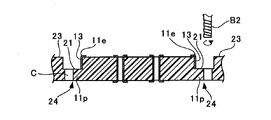
図3~図7は、図1および図2に示すコネクタの製造工程を説明する図である。図3は、切削工程を示す平面図である。
コネクタ1(図1参照)を製造するには、まず絶縁性の基板2を用意する。基板2の材料は、例えば、ガラスエポキシやセラミックである。次に、この基板2に、コネクタ1の形状に沿った溝21を図3に示すように彫る。図に示すように、1枚の基板2からは、複数のコネクタ1を得ることが可能である。切削工程では、貫通孔11hも形成される。
図4は、図3に示す基板の断面を示す断面図である。図4には、1個のコネクタに対応する部分が示されている。
溝21は、例えば、図示しないルータ加工装置に設けられた、回転する棒状の掘削刃であるルータビットB1によって基板2を削ることで形成される。ルータビットB1は、基板2を削り基板2の厚みよりも浅い窪みを形成しながら、コネクタ1の側面11s(図1参照)の形状に沿って一周分に亘り連続して移動する。このようにして、有底の連続した溝21が形成される。ここで、溝21の側面21aは、ルータビットB1が連続して進むことにより形成されているため、一周に亘り滑らかである。
溝21が形成された結果、基板2には、コネクタとなる部分と、その残りの部分であるフレーム23とが形成される。溝21の底に当たる、基板2の厚みよりも薄い部分は、コネクタとなる部分とフレーム23を繋ぐキャリア24として機能する。製造の工程では、複数のコネクタとなる部分がキャリア24を介してフレーム23に一体化した状態で取り扱われる。このため、コネクタとなる部分を個々に分離した状態で取り扱う場合よりも、取扱いが容易であり、量産工程に適用することが可能である。
切削工程を経た基板2は、次に金属メッキ処理される。メッキ工程では、メッキが不要な部分に図示しないレジストが塗布された状態でメッキ液に浸漬される。メッキの材料は例えば銅である。ただしメッキには、銅以外の金属も採用可能である。基板2をメッキ液から取り出した後、レジストを除去することで、目的の部分に金属メッキパターンが形成される。
図5は、メッキ処理後の状態を示す断面図である。
形成された金属メッキパターンのうち、第1の金属メッキパターン12は、コネクタの絶縁基板11となる部分における表面11aの、周縁11eに隣接した領域に帯状に連続的に周回している。また、第2の金属メッキパターン13は第1の金属メッキパターン12に続いている。第2の金属メッキパターン13は、絶縁基板11の側面11s(図2参照)となる部分のうちの、表面11aの周縁11eに隣接した領域を帯状に連続的に周回している。ここで、第2の金属メッキパターン13は、切削工程で形成した溝21の側面21a(図4参照)上に形成されている。先に説明したように、溝21の側面21aは一周に亘り滑らかであるため、この側面21a上に形成された第2の金属メッキパターン13も一周に亘り滑らかである。
また、金属メッキパターンは、貫通孔11hの内壁面を覆い、絶縁基板11の表面11aおよび裏面11bに広がっている。この金属メッキパターンは、電気接続部14(図2参照)における金属メッキ膜141となる。
メッキ工程の後、金属メッキ膜141で覆われた貫通孔11hの内部に導電材料からなる封止材が充填される。その後、熱処理によって、封止材が金属メッキ膜141に溶着する。封止材は、例えば錫を主成分とする半田である。ただし、封止材には、アルミや銀を主成分とする合金も採用可能である。また、封止材は、導電材料に限らず、例えば、商品名「Torr Seal」(登録商標)等の気密性樹脂、その他気密性を確保する材料であってもよい。切削および充填の後、切断が行われる。
図6および図7は、切断工程を説明する図である。図6は平面図であり、図7は断面図である。
切断処理では、キャリア24を切断することにより、フレーム23を取り去る。切断処理では、キャリア24、すなわち切削工程で彫られた溝21の底に当たる部分に、表面11aの周縁11eと比べ外方に膨らんだ膨み部11p、すなわち、第2の金属メッキパターン13よりも膨らんだ膨み部11pが形成されるように切断する。切断処理は、具体的には、切削工程で用いたルータビットB1(図4参照)よりも細径のルータビットB2によって、溝21の底の外周寄りの経路を一周に亘り切削する。ただし切断方法は、細径のルータビットを用いる方法に限られず、例えば切削工程で用いたルータビットB1(図4参照)と同じ径のルータビットで、溝21と重なる程度に溝21から外側にずれた経路を削る方法も採用可能である。また、切断方法には、ルータビットを用いる方法に限られず、例えば、切断する形状に成形された薄刃を押し込むプレス法も採用可能である。
切断工程によってフレーム23が取り去られ、図1および図2に示すコネクタ1が完成する。
切断工程では、第2の金属メッキパターン13よりも膨らんだ膨み部11pを形成するように切断されるので、ルータビットB1や薄刃等の切断工具が、第2の金属メッキパターン13に接触しない。したがって、第2の金属メッキパターン13に、切断工具による凹凸や、傷つきが生じることが避けられる。よって、第2の金属メッキパターン13の滑らかさが維持される。
[取付構造]
図8は、図1および図2に示すコネクタ1の適用例を示す概略構成図である。
図8は、図1および図2に示すコネクタ1の適用例を示す概略構成図である。
図8に示す装置3は、圧力や組成が調整された雰囲気中で動作するチャンバ装置である。より詳細には、装置3は、隔壁31、内部回路基板32、外部回路基板33、そして、図1および図2に示すコネクタ1を備えている。なお、図8では、コネクタ1が、図1に示す表面11aを下に向けて配置されている。
隔壁31は、外部の空間と内部の空間とを仕切る容器である。隔壁31の内部には、内部回路基板32が配置されている。内部回路基板32には減圧または加圧された雰囲気中で動作する電子部品や機構装置が実装されている。隔壁31には、電気配線用の配線穴31hが設けられている。コネクタ1は、配線穴31hよりも大きく、配線穴31hに被さる位置に取り付けられることで配線穴31hを塞いでいる。より詳細には、コネクタ1の絶縁基板11(図1参照)が配線穴31hを塞いでいる。また、コネクタ1は、配線穴31hを介して、隔壁31の内と外との間の電気的接続を担っている。コネクタ1の絶縁基板11と隔壁31との間には、シール材としての半田が充填されている。
外部回路基板33は隔壁31の外部に配置されており、内部回路基板32に電源を供給するとともに、内部回路基板32を制御する。内部回路基板32と外部回路基板33とは、コネクタ1が接続される相手部品である。内部回路基板32および外部回路基板33は、コネクタ1に接触するコンタクト321,331をそれぞれ有している。内部回路基板32と外部回路基板33とは、コネクタ1を介して互いに電気的に接続されている。
隔壁31は、コネクタ1が取り付けられることで気密状態となる。出入口312から空気やガスが排出または注入されることによって、隔壁31内部の圧力が外部よりも減圧または加圧された状態となる。内部回路基板32の電子部品や機構装置はこの圧力の下で動作する。
図9は、図8に示す装置のコネクタ付近を拡大して示す拡大断面図である。なお、図9では、コネクタ1および隔壁31以外の部品は、図示を省略している。
コネクタ1は、半田Sを介して隔壁31に固定されている。固定の方法は、まず、第1の金属メッキパターン12に合わせて環状に成型加工した図示しない半田(プリフォーム半田)を隔壁31の上に載せる。次に、その半田の上に、第1の金属メッキパターン12が半田と接触するように、コネクタ1を載せる。次に、半田を加熱する。半田は加熱することで溶融し、隔壁31および第1の金属メッキパターン12の双方に溶着する。またさらに、溶融した半田は、表面張力によって第2の金属メッキパターン13上にも広がる。このため、第2の金属メッキパターン13と隔壁31との間には、第2の金属メッキパターン13から裾状に広がる半田フィレットFが形成される。コネクタ1と隔壁31との間は、第1の金属メッキパターン12と隔壁31との間の半田による封止に加え、第2の金属メッキパターン13と隔壁31との間に形成された半田フィレットFによってさらに強力に封止される。したがって、気密性が向上し、隔壁31外部と内部との間に圧力差がある状態でも気体の漏れが抑えられる。
しかし、ここで仮に、第2の金属メッキパターンが傷を有したり、側面の周方向に不連続な角を有したりすると、溶融した半田は傷や角による凹凸部分に集まり、半田の分布が不均一になる。この結果、半田が奪われた部分では封止が弱くなる。つまり、第2の金属メッキパターンによって気密性が却って低下するおそれがある。
本実施形態のコネクタ1は、側面11sに、表面11aの周縁11eと比べ外方に膨らんだ膨み部11p、すなわち、第2の金属メッキパターン13よりも膨らんだ膨み部11を有するため、先に説明したように、第2の金属メッキパターン13に傷を付けることなく製造することができる。これにより、このコネクタ1が隔壁31に半田接続される場合には、第2の金属メッキパターン13と隔壁31との間に形成される半田フィレットの厚みを、側面11sの周方向に均一化させることができる。このため、封止が部分的に薄くなる事態が防止される。したがって、本実施形態のコネクタ1は、取り付けられる隔壁の気密性をより向上させることが可能となる。
また、本実施形態のコネクタ1は、側面11sに第2の金属メッキパターン13を有するため、半田フィレットが側面11sに形成される。このため、半田による封止の状態が視認しやすい。
なお、側面に滑らかな形状の第2の金属メッキパターンを形成する方法としては、例えば、突出部のない状態で絶縁基板を切り取り、切り跡をやすり等で平滑化してからメッキ処理することも考えられる。しかし、この場合には、メッキ等すべての工程において、フレームから切り離された、バラバラの状態の絶縁基板を取り扱う必要がある。このような取扱いは、量産工程に適用することが困難である。
本実施形態のコネクタ1は、その製造工程において、コネクタとなる部分をフレーム23に繋いだまま、メッキ等の処理に投入することが可能である。しかも、コネクタとなる部分を複数まとめてフレーム23に繋いだまま処理できる。したがって、量産可能な工程によって滑らかな形状の第2の金属メッキパターンを有するコネクタが製造可能である。
[第2実施形態]
次に、本発明の第2実施形態について説明する。以下の第2実施形態の説明にあたっては、これまで説明してきた実施形態における各要素と同一の要素には符号を省略するか同一の符号を付けて示し、前述の実施形態との相違点について説明する。
次に、本発明の第2実施形態について説明する。以下の第2実施形態の説明にあたっては、これまで説明してきた実施形態における各要素と同一の要素には符号を省略するか同一の符号を付けて示し、前述の実施形態との相違点について説明する。
図10は、本発明の第2実施形態であるコネクタを示す斜視図である。
図10に示すコネクタ4は、表面11aの周縁11eと比べ外方に膨らんだ膨み部41pとして、側面11sから外方の4方向に突出した突起を有する。本実施形態のコネクタ4の膨み部41pは、側面11s上を周回していない。
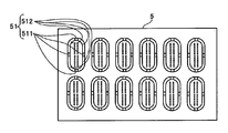
図11は、図10に示すコネクタの製造工程のうち切削工程を示す平面図である。
本実施形態のコネクタ4を製造する切削工程では、第1実施形態の場合と同様、絶縁性の基板5にコネクタの形状に沿った溝51を彫る。ただし、本実施形態に係る切削工程では、周状に延びる溝51のうち、コネクタの部分から四方に延びるキャリア部511を除いた貫通部512は、基板5の表裏面を貫通させる。キャリア部511については、第1実施形態の場合と同様の深さの溝となっている。このような溝51の形状は、例えば、ルータビットの移動の途中で、削る深さを変化させることにより形成される。
図12は、図11に示す基板の断面図である。図12には、キャリア部511を通る断面が示されている。
図11に示す基板5は、第1実施形態の場合と同様に、メッキ工程等を経た後、キャリア部511が切断される。キャリア部511の切断処理では、図10に示すように、表面11aの周縁11eと比べ外方に膨らんだ膨み部41p、すなわち、第2の金属メッキパターン13よりも突出した膨み部41pが形成されるようにキャリア部511を切断する。より詳細には、図12に示す矢印Dの位置を切断する。切断の方法は第1実施形態と同様である。
本実施形態のコネクタ4は、第1実施形態の場合と同様に、表面11aの周縁11eと比べ外方に膨らんだ膨み部41p、すなわち、第2の金属メッキパターン13よりも突出した膨み部41pを有する。このため、切断工程で、切断工具が、第2の金属メッキパターン13に接触しない。したがって、第2の金属メッキパターン13の滑らかさが維持される。よって、本実施形態のコネクタ4も、半田接続による取付構造の気密性をより向上させることが可能となる。
[第3実施形態]
次に、本発明の第3実施形態について説明する。以下の第3実施形態の説明にあたっては、第1実施形態における各要素と同一の要素には符号を省略するか同一の符号を付けて示し、第1実施形態との相違点について説明する。
次に、本発明の第3実施形態について説明する。以下の第3実施形態の説明にあたっては、第1実施形態における各要素と同一の要素には符号を省略するか同一の符号を付けて示し、第1実施形態との相違点について説明する。
図13は、本発明の第3実施形態であるコネクタを示す斜視図である。
図13に示すコネクタ6は、絶縁基板61の表面61aに、周回状に延びた溝613が設けられている。溝613は、第1の金属メッキパターン62よりも幅細であり、表面61aの周縁に周回状に延びている。コネクタ6の第1の金属メッキパターン62は、溝613を覆って周回状に形成されている。より詳細には、溝613は、帯状の第1の金属メッキパターン62の中央近傍に配置されている。
図14は、図13に示すコネクタが隔壁に取り付けられた状態を示す断面図である。
本実施形態のコネクタ6は、第1実施形態の場合と同様に、半田Sを介して隔壁31に固定されている。本実施形態のコネクタ6では、半田Sが溝613の中に入り込む。このため、第1の金属メッキパターン62と隔壁31との間には、半田Sの厚い部分が周回状に形成されている。したがって、第1の金属メッキパターン62と隔壁31の間における気密性がさらに向上する。
また、本実施形態のコネクタ6は、第1の金属メッキパターン62に沿って溝613が設けられているので、隔壁31に取り付けられる際、プリフォーム半田に対する位置決めが容易である。
[第4実施形態]
次に、本発明の第4実施形態について説明する。以下の第4実施形態の説明にあたっては、第1実施形態における各要素と同一の要素には符号を省略するか同一の符号を付けて示し、第1実施形態との相違点について説明する。
次に、本発明の第4実施形態について説明する。以下の第4実施形態の説明にあたっては、第1実施形態における各要素と同一の要素には符号を省略するか同一の符号を付けて示し、第1実施形態との相違点について説明する。
図15は、本発明の第4実施形態であるコネクタを示す斜視図である。
図15に示すコネクタ7も、他の実施形態と同様に、側面71sに、表面11aの周縁11eと比べ外方に膨らんだ膨み部71pを有する。コネクタ7では、側面71sの、表面11aの周縁11eに隣接した領域、すなわち、第2の金属メッキパターン73が設けられた領域が、表面11a側から裏面11b側に近づくほど外方に広がる斜面に形成されている。第2の金属メッキパターン73が設けられた斜面は、表面11aと鈍角をなしている。膨み部71pは、側面71sの、第2の金属メッキパターン73が設けられた斜面と裏面11bの周縁11fとを繋ぐ領域からなる。
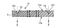
図16は、図15に示すコネクタの製造工程のうち切断工程を示す平面図である。
本実施形態のコネクタ7の製造においては、切削工程で、断面がV字状の溝721を彫り、溝の壁面に金属メッキを施す。これによって、第2の金属メッキパターン73が、表面11a側から裏面11b側に近づくほど外方に広がる斜面に形成されることとなる。
次に、切断工程では、溝721の底よりも内側、すなわちコネクタ7となる部分側の位置を切断する。より詳細には、図16に示す矢印Eの位置を切断する。これによって、図15に示す膨み部71pが形成される。
本実施形態のコネクタ7は、切断工程で、切断工具が、第2の金属メッキパターン73に接触しない。したがって、第2の金属メッキパターン73の滑らかさが維持される。よって、本実施形態のコネクタ7も、半田接続による取付構造の気密性をより向上させることが可能となる。
なお、上述した実施形態には、本発明にいう絶縁基板の例として、角丸長方形の絶縁基板が示されている。ただし、本発明はこれに限られるものではなく、絶縁基板は、例えば楕円形や円形等の他の形状であってもよい。また、絶縁基板は、側面に角を有したり凹部を有してもよい。ただし、第2の金属メッキパターンが形成された領域が、一部が平面であることを許容した外向きに凸の曲面である場合には、半田フィレットの厚みの均一性がより高い。
また、上述した実施形態における第1の金属メッキパターンは太さが一定の帯状である。ただし、本発明はこれに限られるものではなく、第1の金属メッキパターンは、例えば部分的に太さが異なっていてもよい。
また、上述した実施形態における電気接続部14は28個設けられている。ただし、本発明はこれに限られるものではなく、電気接続部の数は28個以外でもよい。また、電気接続部の形状についても、例えば表面および裏面にさらに延伸した部分を有していてもよい。
さらに、コネクタの絶縁基板は、単層基板のみならず、電気接続部が基板の表面および裏面を一直線に貫通していない多層基板であってもよい。
また、上述した実施形態の技術は互いに組み合わせることができる。例えば、第3実施形態のコネクタ6に設けられた溝613は、他の実施形態に設けられてもよい。
1,4,6,7 コネクタ
11,61 絶縁基板
11s,71s 側面
11p,41p,71p 膨み部
11a,61a 表面
11b 裏面
12,62 第1の金属メッキパターン
13,73 第2の金属メッキパターン
14 電気接続部
11,61 絶縁基板
11s,71s 側面
11p,41p,71p 膨み部
11a,61a 表面
11b 裏面
12,62 第1の金属メッキパターン
13,73 第2の金属メッキパターン
14 電気接続部
Claims (6)
- 穴を有する隔壁の該穴に被さる位置に取り付けられて該穴を塞ぐとともに、該穴を介して該隔壁の内と外との間の電気的接続を担うコネクタであって、
絶縁性の材料からなり、前記隔壁に向く表面と、該表面に対する裏面と、該表面の周縁と該裏面の周縁とを繋いで一周する側面とを有し、該側面の、該表面の周縁から該裏面側に離れた領域に、該表面の周縁と比べ外方に膨らんだ膨み部を有する板状の絶縁基板と、 前記表面の、該表面の周縁に隣接した領域を連続的に周回する第1の金属メッキパターンと、
前記側面の、前記表面の周縁に隣接した領域を連続的に周回する第2の金属メッキパターンと、
導電性の材料からなり、前記表面と前記裏面との双方に露出し該表面から該裏面まで電気的に繋がった電気接続部とを備えたことを特徴とするコネクタ。 - 前記膨み部が、前記側面の、前記表面の周縁から前記裏面側に離れた位置に、前記第2の金属めっきパターンよりも側方に突出した突出部であることを特徴とする請求項1記載のコネクタ。
- 前記膨み部が、側面上を周回して延びた突条であることを特徴とする請求項1記載のコネクタ。
- 前記側面の、前記表面の周縁に隣接した領域が、該表面側から該裏面側に向かって外方に広がる斜面に形成され、前記膨み部が、該側面の、該斜面と該裏面の周縁とを繋ぐ領域からなることを特徴とする請求項1記載のコネクタ。
- 前記絶縁基板の側面の、前記第2の金属メッキパターンが形成された領域が、一部が平面であることを許容した外向きに凸の曲面で形成されていることを特徴とする請求項1から4のうちいずれか1項に記載のコネクタ。
- 前記絶縁基板が、前記表面の周縁に周回状に延びた、前記第1の金属メッキパターンよりも幅細の溝を有し、該第1の金属メッキパターンが該溝を覆って周回状に形成されていることを特徴とする請求項1から5のうちのいずれか1項記載のコネクタ。
Priority Applications (1)
| Application Number | Priority Date | Filing Date | Title |
|---|---|---|---|
| CN201280038638.3A CN103718384A (zh) | 2011-08-08 | 2012-07-11 | 连接器 |
Applications Claiming Priority (2)
| Application Number | Priority Date | Filing Date | Title |
|---|---|---|---|
| JP2011-173024 | 2011-08-08 | ||
| JP2011173024A JP5705062B2 (ja) | 2011-08-08 | 2011-08-08 | コネクタ |
Publications (1)
| Publication Number | Publication Date |
|---|---|
| WO2013021774A1 true WO2013021774A1 (ja) | 2013-02-14 |
Family
ID=47668294
Family Applications (1)
| Application Number | Title | Priority Date | Filing Date |
|---|---|---|---|
| PCT/JP2012/067678 Ceased WO2013021774A1 (ja) | 2011-08-08 | 2012-07-11 | コネクタ |
Country Status (3)
| Country | Link |
|---|---|
| JP (1) | JP5705062B2 (ja) |
| CN (1) | CN103718384A (ja) |
| WO (1) | WO2013021774A1 (ja) |
Cited By (1)
| Publication number | Priority date | Publication date | Assignee | Title |
|---|---|---|---|---|
| CN105409063A (zh) * | 2013-07-24 | 2016-03-16 | 罗森伯格高频技术有限及两合公司 | 包括印刷电路板和筒状壳体的系统 |
Families Citing this family (9)
| Publication number | Priority date | Publication date | Assignee | Title |
|---|---|---|---|---|
| JP2014207145A (ja) * | 2013-04-12 | 2014-10-30 | タイコエレクトロニクスジャパン合同会社 | 平板状コネクタおよび隔壁実装構造 |
| JP2014216123A (ja) * | 2013-04-24 | 2014-11-17 | タイコエレクトロニクスジャパン合同会社 | 電気コネクタ組立体及びその実装構造 |
| US9196303B2 (en) * | 2014-03-06 | 2015-11-24 | HGST Netherlands, B.V. | Feedthrough connector for hermetically sealed electronic devices |
| JP6720187B2 (ja) * | 2014-09-16 | 2020-07-08 | アンフェノール・エフシーアイ・アジア・ピーティーイー.・リミテッドAmphenol FCI Asia Pte.Ltd. | 密閉してシールされた電気コネクタアセンブリ |
| US9778705B2 (en) | 2015-09-04 | 2017-10-03 | Apple Inc. | Electronic device with moveable contacts at an exterior surface |
| US10579097B2 (en) | 2015-09-04 | 2020-03-03 | Apple Inc. | Electronic device with contacts flush with housing |
| US9948018B2 (en) | 2015-09-08 | 2018-04-17 | Apple Inc. | Low-profile power and data contacts |
| US10707627B2 (en) | 2017-09-29 | 2020-07-07 | Apple Inc. | Hybrid connector |
| CN114533108A (zh) * | 2022-02-28 | 2022-05-27 | 桂林市啄木鸟医疗器械有限公司 | 电路板模块及其制备方法和牙科x射线机 |
Citations (4)
| Publication number | Priority date | Publication date | Assignee | Title |
|---|---|---|---|---|
| JPS5649068U (ja) * | 1979-09-22 | 1981-05-01 | ||
| JPS6059372U (ja) * | 1983-09-28 | 1985-04-25 | 関西日本電気株式会社 | ロウ付け構体 |
| JPH0395565U (ja) * | 1990-01-19 | 1991-09-30 | ||
| JPH07320800A (ja) * | 1994-05-18 | 1995-12-08 | Star Micronics Co Ltd | 端子及びその製造方法 |
Family Cites Families (5)
| Publication number | Priority date | Publication date | Assignee | Title |
|---|---|---|---|---|
| JP2717313B2 (ja) * | 1989-09-07 | 1998-02-18 | イビデン株式会社 | 電子部品搭載用基板の製造方法 |
| JP3648021B2 (ja) * | 1997-07-23 | 2005-05-18 | 株式会社山武 | 気密端子およびその形成方法 |
| JP4266326B2 (ja) * | 2003-05-21 | 2009-05-20 | タイコエレクトロニクスアンプ株式会社 | 電気接続構造および電気接続システム |
| WO2006129354A1 (ja) * | 2005-06-01 | 2006-12-07 | Matsushita Electric Industrial Co., Ltd. | 回路基板とその製造方法及びこれを用いた電子部品 |
| JP2010170873A (ja) * | 2009-01-23 | 2010-08-05 | Canon Inc | 気密容器及び画像表示装置の製造方法 |
-
2011
- 2011-08-08 JP JP2011173024A patent/JP5705062B2/ja not_active Expired - Fee Related
-
2012
- 2012-07-11 WO PCT/JP2012/067678 patent/WO2013021774A1/ja not_active Ceased
- 2012-07-11 CN CN201280038638.3A patent/CN103718384A/zh active Pending
Patent Citations (4)
| Publication number | Priority date | Publication date | Assignee | Title |
|---|---|---|---|---|
| JPS5649068U (ja) * | 1979-09-22 | 1981-05-01 | ||
| JPS6059372U (ja) * | 1983-09-28 | 1985-04-25 | 関西日本電気株式会社 | ロウ付け構体 |
| JPH0395565U (ja) * | 1990-01-19 | 1991-09-30 | ||
| JPH07320800A (ja) * | 1994-05-18 | 1995-12-08 | Star Micronics Co Ltd | 端子及びその製造方法 |
Cited By (1)
| Publication number | Priority date | Publication date | Assignee | Title |
|---|---|---|---|---|
| CN105409063A (zh) * | 2013-07-24 | 2016-03-16 | 罗森伯格高频技术有限及两合公司 | 包括印刷电路板和筒状壳体的系统 |
Also Published As
| Publication number | Publication date |
|---|---|
| JP5705062B2 (ja) | 2015-04-22 |
| CN103718384A (zh) | 2014-04-09 |
| JP2013037890A (ja) | 2013-02-21 |
Similar Documents
| Publication | Publication Date | Title |
|---|---|---|
| JP5705062B2 (ja) | コネクタ | |
| JP6006474B2 (ja) | 配線基板、多数個取り配線基板、およびその製造方法 | |
| EP3349243B1 (en) | Package for housing electronic component, electronic device, and electronic module | |
| US20200043866A1 (en) | Module | |
| US7142435B2 (en) | Lid for use in packaging an electronic device and method of manufacturing the lid | |
| CN107740065A (zh) | 一种掩模版及其成膜方法、成膜设备 | |
| TWI546869B (zh) | Manufacturing method of semiconductor device | |
| JP2012230945A5 (ja) | ||
| US20220416759A1 (en) | Piezoelectric vibration plate, piezoelectric vibration device, and manufacturing method for piezoelectric vibration device | |
| TWM547185U (zh) | 選擇性電磁遮蔽封裝體結構 | |
| TWI546871B (zh) | Manufacturing method of semiconductor device | |
| CN1205743C (zh) | 用于表面声波器件的阵列处理的系统和方法 | |
| US12177983B2 (en) | Electronic component housing package, electronic device, and electronic module | |
| JP7130958B2 (ja) | モジュール | |
| US11398432B2 (en) | Wiring substrate and electronic device | |
| US10405430B2 (en) | Ceramic substrate, electronic component, and method of manufacturing ceramic substrate | |
| JP2012028454A (ja) | 部分めっき方法、金属製蓋部材、および電子部品。 | |
| JP5922447B2 (ja) | 多数個取り配線基板 | |
| JP2018107282A (ja) | 配線基板 | |
| TW200946012A (en) | Electromagnetic interference shield | |
| JP2001144201A (ja) | 電子部品装置 | |
| US12155367B2 (en) | Method for manufacturing ceramic substrate and ceramic substrate | |
| JPH10303324A (ja) | 電子部品容器 | |
| KR20150061368A (ko) | 반도체 패키지 및 그의 제조 방법 | |
| TW201838133A (zh) | 選擇性電磁遮蔽封裝體結構及其製法 |
Legal Events
| Date | Code | Title | Description |
|---|---|---|---|
| 121 | Ep: the epo has been informed by wipo that ep was designated in this application |
Ref document number: 12822650 Country of ref document: EP Kind code of ref document: A1 |
|
| NENP | Non-entry into the national phase |
Ref country code: DE |
|
| 122 | Ep: pct application non-entry in european phase |
Ref document number: 12822650 Country of ref document: EP Kind code of ref document: A1 |