WO2013008482A1 - 太陽電池およびその製造方法 - Google Patents
太陽電池およびその製造方法 Download PDFInfo
- Publication number
- WO2013008482A1 WO2013008482A1 PCT/JP2012/052464 JP2012052464W WO2013008482A1 WO 2013008482 A1 WO2013008482 A1 WO 2013008482A1 JP 2012052464 W JP2012052464 W JP 2012052464W WO 2013008482 A1 WO2013008482 A1 WO 2013008482A1
- Authority
- WO
- WIPO (PCT)
- Prior art keywords
- thin film
- silicon thin
- type
- solar cell
- type silicon
- Prior art date
- Legal status (The legal status is an assumption and is not a legal conclusion. Google has not performed a legal analysis and makes no representation as to the accuracy of the status listed.)
- Ceased
Links
Images



Classifications
-
- H—ELECTRICITY
- H10—SEMICONDUCTOR DEVICES; ELECTRIC SOLID-STATE DEVICES NOT OTHERWISE PROVIDED FOR
- H10F—INORGANIC SEMICONDUCTOR DEVICES SENSITIVE TO INFRARED RADIATION, LIGHT, ELECTROMAGNETIC RADIATION OF SHORTER WAVELENGTH OR CORPUSCULAR RADIATION
- H10F10/00—Individual photovoltaic cells, e.g. solar cells
- H10F10/10—Individual photovoltaic cells, e.g. solar cells having potential barriers
- H10F10/16—Photovoltaic cells having only PN heterojunction potential barriers
- H10F10/164—Photovoltaic cells having only PN heterojunction potential barriers comprising heterojunctions with Group IV materials, e.g. ITO/Si or GaAs/SiGe photovoltaic cells
- H10F10/165—Photovoltaic cells having only PN heterojunction potential barriers comprising heterojunctions with Group IV materials, e.g. ITO/Si or GaAs/SiGe photovoltaic cells the heterojunctions being Group IV-IV heterojunctions, e.g. Si/Ge, SiGe/Si or Si/SiC photovoltaic cells
-
- H—ELECTRICITY
- H10—SEMICONDUCTOR DEVICES; ELECTRIC SOLID-STATE DEVICES NOT OTHERWISE PROVIDED FOR
- H10F—INORGANIC SEMICONDUCTOR DEVICES SENSITIVE TO INFRARED RADIATION, LIGHT, ELECTROMAGNETIC RADIATION OF SHORTER WAVELENGTH OR CORPUSCULAR RADIATION
- H10F10/00—Individual photovoltaic cells, e.g. solar cells
- H10F10/10—Individual photovoltaic cells, e.g. solar cells having potential barriers
- H10F10/12—Photovoltaic cells having only metal-insulator-semiconductor [MIS] potential barriers
-
- H—ELECTRICITY
- H10—SEMICONDUCTOR DEVICES; ELECTRIC SOLID-STATE DEVICES NOT OTHERWISE PROVIDED FOR
- H10F—INORGANIC SEMICONDUCTOR DEVICES SENSITIVE TO INFRARED RADIATION, LIGHT, ELECTROMAGNETIC RADIATION OF SHORTER WAVELENGTH OR CORPUSCULAR RADIATION
- H10F10/00—Individual photovoltaic cells, e.g. solar cells
- H10F10/10—Individual photovoltaic cells, e.g. solar cells having potential barriers
- H10F10/16—Photovoltaic cells having only PN heterojunction potential barriers
- H10F10/164—Photovoltaic cells having only PN heterojunction potential barriers comprising heterojunctions with Group IV materials, e.g. ITO/Si or GaAs/SiGe photovoltaic cells
- H10F10/165—Photovoltaic cells having only PN heterojunction potential barriers comprising heterojunctions with Group IV materials, e.g. ITO/Si or GaAs/SiGe photovoltaic cells the heterojunctions being Group IV-IV heterojunctions, e.g. Si/Ge, SiGe/Si or Si/SiC photovoltaic cells
- H10F10/166—Photovoltaic cells having only PN heterojunction potential barriers comprising heterojunctions with Group IV materials, e.g. ITO/Si or GaAs/SiGe photovoltaic cells the heterojunctions being Group IV-IV heterojunctions, e.g. Si/Ge, SiGe/Si or Si/SiC photovoltaic cells the Group IV-IV heterojunctions being heterojunctions of crystalline and amorphous materials, e.g. silicon heterojunction [SHJ] photovoltaic cells
-
- H—ELECTRICITY
- H10—SEMICONDUCTOR DEVICES; ELECTRIC SOLID-STATE DEVICES NOT OTHERWISE PROVIDED FOR
- H10F—INORGANIC SEMICONDUCTOR DEVICES SENSITIVE TO INFRARED RADIATION, LIGHT, ELECTROMAGNETIC RADIATION OF SHORTER WAVELENGTH OR CORPUSCULAR RADIATION
- H10F10/00—Individual photovoltaic cells, e.g. solar cells
- H10F10/10—Individual photovoltaic cells, e.g. solar cells having potential barriers
- H10F10/17—Photovoltaic cells having only PIN junction potential barriers
- H10F10/174—Photovoltaic cells having only PIN junction potential barriers comprising monocrystalline or polycrystalline materials
-
- H—ELECTRICITY
- H10—SEMICONDUCTOR DEVICES; ELECTRIC SOLID-STATE DEVICES NOT OTHERWISE PROVIDED FOR
- H10F—INORGANIC SEMICONDUCTOR DEVICES SENSITIVE TO INFRARED RADIATION, LIGHT, ELECTROMAGNETIC RADIATION OF SHORTER WAVELENGTH OR CORPUSCULAR RADIATION
- H10F71/00—Manufacture or treatment of devices covered by this subclass
- H10F71/121—The active layers comprising only Group IV materials
- H10F71/1224—The active layers comprising only Group IV materials comprising microcrystalline silicon
-
- Y—GENERAL TAGGING OF NEW TECHNOLOGICAL DEVELOPMENTS; GENERAL TAGGING OF CROSS-SECTIONAL TECHNOLOGIES SPANNING OVER SEVERAL SECTIONS OF THE IPC; TECHNICAL SUBJECTS COVERED BY FORMER USPC CROSS-REFERENCE ART COLLECTIONS [XRACs] AND DIGESTS
- Y02—TECHNOLOGIES OR APPLICATIONS FOR MITIGATION OR ADAPTATION AGAINST CLIMATE CHANGE
- Y02E—REDUCTION OF GREENHOUSE GAS [GHG] EMISSIONS, RELATED TO ENERGY GENERATION, TRANSMISSION OR DISTRIBUTION
- Y02E10/00—Energy generation through renewable energy sources
- Y02E10/50—Photovoltaic [PV] energy
- Y02E10/545—Microcrystalline silicon PV cells
-
- Y—GENERAL TAGGING OF NEW TECHNOLOGICAL DEVELOPMENTS; GENERAL TAGGING OF CROSS-SECTIONAL TECHNOLOGIES SPANNING OVER SEVERAL SECTIONS OF THE IPC; TECHNICAL SUBJECTS COVERED BY FORMER USPC CROSS-REFERENCE ART COLLECTIONS [XRACs] AND DIGESTS
- Y02—TECHNOLOGIES OR APPLICATIONS FOR MITIGATION OR ADAPTATION AGAINST CLIMATE CHANGE
- Y02E—REDUCTION OF GREENHOUSE GAS [GHG] EMISSIONS, RELATED TO ENERGY GENERATION, TRANSMISSION OR DISTRIBUTION
- Y02E10/00—Energy generation through renewable energy sources
- Y02E10/50—Photovoltaic [PV] energy
- Y02E10/547—Monocrystalline silicon PV cells
-
- Y—GENERAL TAGGING OF NEW TECHNOLOGICAL DEVELOPMENTS; GENERAL TAGGING OF CROSS-SECTIONAL TECHNOLOGIES SPANNING OVER SEVERAL SECTIONS OF THE IPC; TECHNICAL SUBJECTS COVERED BY FORMER USPC CROSS-REFERENCE ART COLLECTIONS [XRACs] AND DIGESTS
- Y02—TECHNOLOGIES OR APPLICATIONS FOR MITIGATION OR ADAPTATION AGAINST CLIMATE CHANGE
- Y02E—REDUCTION OF GREENHOUSE GAS [GHG] EMISSIONS, RELATED TO ENERGY GENERATION, TRANSMISSION OR DISTRIBUTION
- Y02E10/00—Energy generation through renewable energy sources
- Y02E10/50—Photovoltaic [PV] energy
- Y02E10/548—Amorphous silicon PV cells
-
- Y—GENERAL TAGGING OF NEW TECHNOLOGICAL DEVELOPMENTS; GENERAL TAGGING OF CROSS-SECTIONAL TECHNOLOGIES SPANNING OVER SEVERAL SECTIONS OF THE IPC; TECHNICAL SUBJECTS COVERED BY FORMER USPC CROSS-REFERENCE ART COLLECTIONS [XRACs] AND DIGESTS
- Y02—TECHNOLOGIES OR APPLICATIONS FOR MITIGATION OR ADAPTATION AGAINST CLIMATE CHANGE
- Y02P—CLIMATE CHANGE MITIGATION TECHNOLOGIES IN THE PRODUCTION OR PROCESSING OF GOODS
- Y02P70/00—Climate change mitigation technologies in the production process for final industrial or consumer products
- Y02P70/50—Manufacturing or production processes characterised by the final manufactured product
Definitions
- the present invention relates to a so-called hybrid solar cell having a structure in which a silicon thin film is formed on a crystalline silicon substrate, and a method for manufacturing the same.
- a solar cell having a structure in which an amorphous silicon thin film is stacked on a crystalline silicon substrate, i-type (ie, intrinsic) amorphous silicon thin films are formed on both sides of the crystalline silicon substrate,
- Batteries are well known (see, for example, Patent Document 1).
- a transparent conductive film and a comb-shaped electrode for taking out a photocurrent are formed on the outer sides of the p-type and n-type amorphous silicon thin films, respectively.
- the amorphous silicon thin film is conventionally decomposed by discharge decomposition using silane gas (SiH 4 ) and hydrogen gas (H 2 ) as source gases by a capacitively coupled plasma CVD method that generates plasma by capacitive coupling. Is formed by depositing on the substrate. Further, when forming p-type and n-type doped thin films, diborane (B 2 H 6 ) and phosphine (PH 3 ) are used in a small amount mixed with the source gas, respectively.
- the carrier lifetime of the solar cell can be extended, thereby increasing the open-circuit voltage of the solar cell and improving the conversion efficiency.
- the gas decomposition efficiency by high frequency discharge in the capacitively coupled plasma CVD method is low, and therefore, in a film forming process using silane and hydrogen as hydrides as raw materials, excessive hydrogen is contained in the thin film. This is also a factor that reduces the carrier life.
- the present invention can form a thin film that has few defects and does not contain excessive hydrogen during film formation, and further compensates for defects generated during film formation after film formation to reduce defects in the interface and the thin film.
- the main object is to provide a method of manufacturing a solar cell that can achieve a long carrier life.
- the manufacturing method according to the present invention is a manufacturing method of a solar cell having a structure in which a silicon thin film is formed on a crystalline silicon substrate, wherein the crystalline silicon substrate is formed by an inductively coupled plasma CVD method for generating plasma by inductive coupling. Further, a thin film forming step of forming a microcrystalline silicon thin film including a fine silicon crystal as the silicon thin film, and the microcrystalline silicon thin film formed on the crystalline silicon substrate are 5 ⁇ 10 5 Pa or more. And a steam heat treatment step of performing a heat treatment in a steam atmosphere of pressure.
- the temperature of the crystalline silicon substrate in the thin film forming step is preferably 100 ° C. to 300 ° C.
- the temperature in the steam heat treatment step is preferably 150 to 300 ° C.
- the steam pressure is preferably 5 ⁇ 10 5 Pa to 1.5 ⁇ 10 6 Pa
- the treatment time is preferably 0.5 to 3 hours.
- the solar cell forms i-type silicon thin films on both surfaces of a crystalline silicon substrate, forms a p-type silicon thin film on the surface of one i-type silicon thin film, and forms the surface of the other i-type silicon thin film.
- the fine film of the type is used as at least one of the i-type silicon thin film, the p-type silicon thin film, and the n-type silicon thin film by the thin film formation step.
- a crystalline silicon thin film may be formed, and then the water vapor heat treatment step may be performed.
- the thin film formation is performed.
- the i-type microcrystalline silicon thin film may be formed as the i-type silicon thin film, and then the water vapor heat treatment process may be performed.
- the inductively coupled plasma CVD method is used in the thin film formation step, the gas decomposition efficiency is high and the plasma potential can be kept low. Therefore, it is possible to form a thin film that has few defects during film formation and does not contain excessive hydrogen. Thereby, a long carrier life can be realized.
- microcrystalline silicon thin film formation and the steam heat treatment by combining the microcrystalline silicon thin film formation and the steam heat treatment, a longer carrier life can be realized as compared with the case of combining the amorphous silicon thin film formation and the steam heat treatment.
- the invention according to claim 2 has the following further effects. That is, by setting the temperature of the crystalline silicon substrate in the thin film forming process to 100 ° C. to 300 ° C., the separation and diffusion of hydrogen in the thin film during film formation can be suppressed, so that the microcrystalline silicon thin film with fewer defects Can be formed. Therefore, a longer carrier life can be realized.
- the steam heat treatment described above is performed by setting the temperature in the steam heat treatment step to 150 to 300 ° C., the steam pressure to 5 ⁇ 10 5 Pa to 1.5 ⁇ 10 6 Pa, and the treatment time to 0.5 to 3 hours. The effect of this can be exhibited effectively.
- the i-type silicon thin film in this solar cell is mainly intended to prevent the diffusion of impurities from the p-type or n-type doped silicon thin film and extend the carrier life at the interface.
- the i-type microcrystalline silicon thin film as the i-type silicon thin film by the thin film forming step, and then performing the water vapor heat treatment step, the defects in the interface and the thin film can be reduced as described above. Since the lifetime can be extended, the main purpose of the i-type thin film can be achieved more effectively.
- an amorphous silicon thin film doped with n-type or p-type has a low activation rate of impurities and it is difficult to form a low-resistance film.
- an n-type or p-type doped microcrystalline silicon thin film has a high impurity activation rate and can form a low-resistance film with a small amount of impurities. Therefore, since the defect formation probability can be reduced, a solar cell having a large open circuit voltage and short circuit current and high conversion efficiency can be obtained.
- the following further effect is obtained. That is, by forming the i-type microcrystalline silicon thin film as the i-type silicon thin film by the thin film forming step, and then performing the steam heat treatment step, the defects in the interface and the thin film are reduced as described above. In addition, a long carrier life can be realized, so that a solar cell with higher conversion efficiency can be obtained.
- the manufacturing method according to the present invention is a method for manufacturing a solar cell having a structure in which a silicon thin film is formed on a crystalline silicon substrate (for example, a structure in which a silicon thin film 52 is formed on a crystalline silicon substrate 50 shown in FIG. 2).
- a process in which the microcrystalline silicon thin film is formed on a substrate is provided with a steam heat treatment step in which heat treatment is performed in a steam atmosphere at a pressure of 5 ⁇ 10 5 Pa or more.
- the silicon thin film is formed directly on the surface of the crystalline silicon substrate without interposing another thin film, or formed by interposing another thin film. Including both. Accordingly, in the thin film formation step, the microcrystalline silicon thin film may be formed directly on the surface of the crystalline silicon substrate without interposing another thin film, or may be formed with another thin film interposed. For example, forming the microcrystalline silicon thin film as the silicon thin film 52 shown in FIG. 2, the silicon thin films 54 and 56 shown in FIG. 5, and the silicon thin film 74 shown in FIG. 6 is a more specific example in the former case. Forming a microcrystalline silicon thin film as the silicon thin films 58 and 60 shown in FIG. 5 is a more specific example of the latter case.
- the crystalline silicon substrate may be a single crystal silicon substrate or a polycrystalline silicon substrate.
- the conductivity type may be p-type or n-type.
- a plasma CVD apparatus as shown in FIG. 1 can be used.
- a plasma 40 is generated by an induction electric field generated by flowing a high-frequency current from a high-frequency power source 42 through a planar conductor (in other words, a planar antenna; the same applies hereinafter) 34, and the substrate 50 is generated using the plasma 40.
- a planar conductor in other words, a planar antenna; the same applies hereinafter
- the above is an inductively coupled plasma CVD apparatus for forming a thin film by an inductively coupled plasma CVD method.
- the substrate 50 is specifically the above crystalline silicon substrate.
- This plasma CVD apparatus is provided with, for example, a metal vacuum vessel 22, and the inside thereof is evacuated by a evacuation apparatus 24.
- a raw material gas 28 corresponding to the processing content to be applied to the substrate 20 is introduced through a gas introduction pipe 26.
- the source gas 28 is, for example, silane gas (strictly speaking, monosilane gas SiH 4 ) or silane gas diluted with hydrogen or a rare gas (eg, helium, neon, argon, etc.). The case of doping impurities will be described later.
- a holder 30 that holds the substrate 50 is provided in the vacuum vessel 22 .
- a heater 32 for heating the substrate 50 to a desired temperature is provided in the holder 30.
- a planar conductor 34 having a rectangular planar shape is provided in the vacuum vessel 22, more specifically, inside the ceiling surface 23 of the vacuum vessel 22 so as to face the substrate holding surface of the holder 30.
- the planar shape of the planar conductor 34 may be a rectangle, a square, or the like.
- the specific shape of the planar shape may be determined according to the planar shape of the substrate 50, for example.
- High-frequency power is supplied from the high-frequency power source 42 via the matching circuit 44 and via the power supply electrode 36 and the termination electrode 38 between the power supply end on one end side in the longitudinal direction of the planar conductor 34 and the terminal end on the other end side. As a result, a high-frequency current flows through the planar conductor 34.
- the frequency of the high-frequency power output from the high-frequency power source 42 is, for example, a general 13.56 MHz, but is not limited to this.
- the power supply electrode 36 and the termination electrode 38 are attached to the ceiling surface 23 of the vacuum vessel 22 via insulating flanges 39, respectively. Between these elements, packings for vacuum sealing are provided.
- the upper portion of the ceiling surface 23 is preferably covered with a shield box 46 that prevents high-frequency leakage as in this example.
- a high-frequency magnetic field is generated around the planar conductor 34, thereby generating an induced electric field in the direction opposite to the high-frequency current. Due to this induced electric field, electrons are accelerated in the vacuum chamber 22 to ionize the gas 28 in the vicinity of the planar conductor 34, and plasma 40 is generated in the vicinity of the planar conductor 34.
- the plasma 40 diffuses to the vicinity of the substrate 50, and a thin film can be formed on the substrate 50 by the plasma 40 by an inductively coupled plasma CVD method.
- a microcrystalline silicon thin film containing minute silicon crystals can be formed on the crystalline silicon substrate 50.
- microcrystalline silicon thin film formed by the plasma CVD method as described above contains hydrogen, it is strictly called a hydrogenated microcrystalline silicon ( ⁇ c-Si: H or nc-Si: H) thin film. The same applies to the microcrystalline silicon thin film described below.
- a large amount of hydrogen radicals may be generated in the plasma 40 to promote crystallization of silicon.
- the amount of high-frequency power input from the high-frequency power source 42 is increased, and the gas pressure in the vacuum container 22 is set low so that the generated hydrogen radicals can easily reach the surface of the substrate 50.
- a method of increasing the hydrogen partial pressure may be employed.
- the inductively coupled plasma CVD method used in the thin film formation process can generate a large induced electric field in the plasma, and therefore has a higher gas decomposition efficiency than the capacitively coupled plasma CVD method. Can be formed.
- the inductively coupled plasma CVD method is a method of generating plasma by an induction electric field generated by flowing a high frequency current through the antenna, a high frequency voltage is applied between two parallel electrodes, Compared with a capacitively coupled plasma CVD method in which plasma is generated using a generated high-frequency electric field, the plasma potential can be kept low, and ion bombardment on the substrate surface and the deposited thin film can be reduced. As a result, it is possible to reduce defects created in the interface with the substrate and in the deposited thin film during film formation.
- the temperature of the crystalline silicon substrate in the thin film forming process is set to a relatively low temperature of 100 ° C. to 300 ° C., thereby suppressing the separation and diffusion of hydrogen in the thin film during film formation.
- a microcrystalline silicon thin film with few defects can be formed. Therefore, a longer carrier life can be realized.
- the temperature in the steam heat treatment step is preferably 150 ° C. to 300 ° C.
- the steam pressure is preferably 5 ⁇ 10 5 Pa to 1.5 ⁇ 10 6 Pa
- the treatment time is preferably 0.5 hours to 3 hours. The effect of the steam heat treatment can be exhibited effectively.
- a silicon thin film 52 was formed on the crystalline silicon substrate 50.
- a single crystal silicon substrate was used as the crystal silicon substrate 50.
- an inductively coupled plasma CVD apparatus that is, an inductively coupled plasma CVD method as shown in FIG. 1 was used.
- 100% silane gas (SiH 4 ) was used as the source gas 28.
- the temperature of the substrate 50 during film formation was set to 150 ° C.
- the carrier lifetime of the interface of the said sample and the other sample for a comparison was measured by the photo-induced carrier microwave absorption method. More specifically, the effective light-induced minority carrier lifetime when the surface of the sample was constantly irradiated with LED light having a center wavelength of 620 nm and a light intensity of 1.5 mW / cm 2 was measured.
- the carrier lifetime of the surface of the crystalline silicon substrate 50 (ie, the bare silicon surface) from which the natural oxide film was removed with diluted hydrofluoric acid was 20 ⁇ s (Comparative Example 4).
- the carrier lifetime after the above-described steam heat treatment was further applied to the same crystalline silicon substrate 50 was 700 ⁇ s (Comparative Example 5).
- the temperature in the steam heat treatment step was 210 ° C.
- the steam pressure was 1 ⁇ 10 5 Pa
- the treatment time was 3 hours. The same applies to Comparative Example 3 and Example 1 described later.
- the carrier lifetime at the interface is 27 ⁇ s and 10 nm when the film thickness is 3 nm. It was sometimes 35 ⁇ s and 78 ⁇ s at 50 nm (Comparative Example 2).
- the Raman scattering spectrum of the silicon thin film 52 having a film thickness of 50 nm was measured by Raman spectroscopy, as shown in the graph A in FIG. 4, the peak indicating crystalline silicon at a position in the vicinity of a wave number of 520 cm ⁇ 1 is It could not be confirmed, and only a peak corresponding to amorphous silicon that broadly spreads around the wave number of 480 cm ⁇ 1 was confirmed.
- the carrier life after the steam heat treatment described above was further applied to the same sample as in Comparative Example 2 was 82 ⁇ s when the film thickness was 3 nm, 250 ⁇ s when 10 nm, and 910 ⁇ s when 50 nm (Comparative Example 3). .
- a very long carrier life (1360 ⁇ s) can be obtained by combining the formation of the microcrystalline silicon thin film by the inductively coupled plasma CVD method and the steam heat treatment as in Example 1. That is, it is longer than the case where the bare silicon surface is combined with the steam heat treatment (Comparative Example 5), and further, the carrier life is longer than when the amorphous silicon thin film formation is combined with the steam heat treatment (Comparative Example 3). I was able to.
- the carrier lifetime is 58 ⁇ s.
- the carrier life after the same sample was further subjected to steam heat treatment was 338 ⁇ s (Example 1). That is, also in this case, a long carrier life can be realized by combining the formation of the microcrystalline silicon thin film by the inductively coupled plasma CVD method and the steam heat treatment.
- the basic structure of the solar cell shown in FIG. 5 is well known (see, for example, Patent Document 1) and is i-type (that is, intrinsically doped with no impurities) on both sides of the crystalline silicon substrate 50.
- the silicon thin films 54 and 56 are formed, the p-type silicon thin film 58 is formed on the surface of one i-type silicon thin film 54, and the n-type silicon is formed on the surface of the other i-type silicon thin film 56. It has a structure in which a thin film 60 is formed.
- transparent conductive films 62 and 64 are formed on the surfaces of the silicon thin films 58 and 60, respectively, and comb-shaped electrodes 66 and 68 for extracting a photocurrent are formed on the outer surfaces thereof.
- the crystalline silicon substrate 50 is usually n-type, but may be p-type. For example, the light 10 is incident from the transparent conductive film 62 side.
- the i-type microcrystalline silicon thin film is formed as the i-type silicon thin films 54 and 56 by the thin film forming step, and then the steam heat treatment step is performed.
- the p-type microcrystalline silicon thin film and the n-type microcrystalline silicon thin film are respectively formed as the p-type silicon thin film 58 and the n-type silicon thin film 60 by the thin film forming step. And then performing the steam heat treatment step.
- the source gas 28 may be mixed with a gas containing a desired dopant.
- a gas containing a desired dopant For example, an appropriate amount of diborane (B 2 H 6 ) may be mixed when the p-type silicon thin film 58 is formed, and an appropriate amount of phosphine (PH 3 ) may be mixed when the n-type silicon thin film 60 is formed.
- the film formation on the crystalline silicon substrate 50 may be performed on one side or on both sides simultaneously. Specifically, it may be determined according to the configuration of an apparatus for performing film formation or the like.
- Crystalline silicon substrate 50 ⁇ i-type silicon thin film 54 formation ⁇ i-type silicon thin film 56 formation ⁇ p-type silicon thin film 58 formation ⁇ n-type silicon thin film 60 formation ⁇ transparent conductive film 62 formation ⁇ transparent conductive film 64 formation ⁇ electrode 66 formation ⁇ electrode 68 formation ⁇ water vapor heat treatment.
- the present invention is not limited to this.
- Crystalline silicon substrate 50 ⁇ i-type silicon thin films 54 and 56 formation ⁇ p-type silicon thin film 58 formation ⁇ n-type silicon thin film 60 formation ⁇ transparent conductive film 62 , 64 formation ⁇ electrode 66 formation ⁇ electrode 68 formation ⁇ water vapor heat treatment.
- the present invention is not limited to this.
- the i-type silicon thin films 54 and 56 in the solar cell are mainly intended to prevent the diffusion of impurities from the p-type or n-type doped silicon thin films 58 and 60 and to extend the carrier life at the interface.
- the i-type microcrystalline silicon thin film is formed as the i-type silicon thin films 54 and 56 by the thin film forming process, and then the steam heat treatment process is performed. By doing so, the interface and the defects in the thin film can be reduced and the carrier life can be increased as described above, so that the main purpose of the i-type thin films 54 and 56 can be achieved more effectively.
- an amorphous silicon thin film doped n-type or p-type was formed as the silicon thin film 58, 60, but it was doped n-type or p-type.
- the amorphous silicon thin film has a low activation rate of impurities and it is difficult to form a low resistance film, and there is a problem that if the impurity is increased to reduce the resistance, it becomes a defect and the carrier life is shortened.
- an n-type or p-type doped microcrystalline silicon thin film is formed as the silicon thin film 58 or 60 as in the method shown in the above (b) or (c)
- the n-type or p-type is formed.
- the doped microcrystalline silicon thin film has a high impurity activation rate, and a low resistance film can be formed with a small amount of impurities. Therefore, since the defect formation probability can be reduced, a solar cell having a large open circuit voltage and short circuit current and high conversion efficiency can be obtained.
- an i-type silicon thin film 74 is formed on one surface of a crystalline silicon substrate 50, and a first electrode 76 and a second electrode 78 having different work functions are formed on the silicon thin film 74. It has a formed structure. Both electrodes 76 and 78 have, for example, a comb shape.
- a transparent protective film 72 made of a silicon oxide film or a silicon nitride film is formed on the other surface of the crystalline silicon substrate 50.
- the crystalline silicon substrate 50 may be n-type or p-type. In this example, the light 10 is incident from the transparent protective film 72 side.
- the first electrode 76 is a metal having a work function smaller than that of the crystalline silicon substrate 50 and the second electrode 78, such as aluminum (Al (), hafnium (Hf), tantalum (Ta), indium (In), zirconium. It is made of a metal such as (Zr).
- the second electrode 78 is made of a metal having a work function larger than that of the crystalline silicon substrate 50 and the first electrode 76, such as gold (Au), nickel (Ni), platinum (Pt), palladium (Pd), etc. It is made of metal.
- a MIS (metal / insulating thin film / semiconductor) structure is formed by the electrode 76, the silicon thin film 74, and the crystalline silicon substrate 50, and a MIS structure is also formed by the electrode 78, the silicon thin film 74, and the crystalline silicon substrate 50.
- a double MIS structure is used, and by using the work function difference between this and the electrodes 76 and 78, power can be generated efficiently.
- the i-type microcrystalline silicon thin film is formed as the i-type silicon thin film 74 by the thin film forming step, and then the steam heat treatment step is performed.
- the transparent protective film 72 a known film formation technique may be used.
- Crystalline silicon substrate 50 ⁇ transparent protective film 72 formation ⁇ removal of oxide film on the lower surface of crystal silicon substrate 50 (surface on silicon thin film 74 side) ⁇ silicon thin film 74 formation ⁇ electrode 76 formation ⁇ electrode 78 formation ⁇ steam heat treatment.
- the present invention is not limited to this.
- the thin film forming step forms the i-type microcrystalline silicon thin film as the i-type silicon thin film 74, and then executes the steam heat treatment step as described above.
- the thin film forming step forms the i-type microcrystalline silicon thin film as the i-type silicon thin film 74, and then executes the steam heat treatment step as described above.
- the solar cell manufactured by each manufacturing method described above can achieve high conversion efficiency for the reasons described above.
Landscapes
- Photovoltaic Devices (AREA)
- Chemical & Material Sciences (AREA)
- Crystallography & Structural Chemistry (AREA)
Abstract
この発明は、成膜時に欠陥が少なくかつ過分な水素を含まない薄膜形成を行うことができ、更に成膜時に発生する欠陥を成膜後に補償して界面および薄膜中の欠陥を減少させることができ、それによって長いキャリア寿命を実現することを主目的としている。 結晶シリコン基板50上にシリコン薄膜52を形成した構造を有する太陽電池の製造方法である。この製造方法は、誘導結合によってプラズマを生成する誘導結合型のプラズマCVD法によって、結晶シリコン基板50上に、シリコン薄膜52として、微小なシリコン結晶を含む微結晶シリコン薄膜を形成する薄膜形成工程と、この微結晶シリコン薄膜を形成したものに、5×10⁵ Pa以上の圧力の水蒸気雰囲気中で熱処理を施す水蒸気熱処理工程とを備えている。
Description
この発明は、結晶シリコン基板上にシリコン薄膜を形成した構造を有する、いわゆるハイブリッド型の太陽電池およびその製造方法に関する。
結晶シリコン基板に非晶質(アモルファス)シリコン薄膜を積層した構造を有する太陽電池の一例として、結晶シリコン基板の両面にi型の(即ち真性の)非晶質シリコン薄膜を形成し、かつ一方のi型の非晶質シリコン薄膜の表面にp型の非晶質シリコン薄膜を形成し、他方のi型の非晶質シリコン薄膜の表面にn型の非晶質シリコン薄膜を形成した構造の太陽電池が良く知られている(例えば特許文献1参照)。
上記p型、n型の非晶質シリコン薄膜の更に外側には、透明導電膜および光電流を取り出すためのくし型の電極がそれぞれ形成されている。
上記非晶質シリコン薄膜は、従来は、容量結合によってプラズマを生成する容量結合型のプラズマCVD法によって、シランガス(SiH4 )および水素ガス(H2 )を原料ガスとして用いて、これを放電分解によって基板上に堆積させることによって形成されている。また、p型、n型のドープ薄膜を形成するときには、それぞれジボラン(B2H6 )、ホスフィン(PH3 )が、上記原料ガスに少量混合されて使用される。
結晶シリコン基板上において、コンタクト層である上記p型、n型の非晶質シリコン薄膜との間に、不純物がドープされていない上記i型の非晶質シリコン薄膜を挿入することによって、界面でのキャリア寿命を延ばすことができ、それによって、太陽電池の開放電圧を大きくして、変換効率を向上させることができることが知られている。
非晶質シリコンの物性で良く知られているように、薄膜中の水素はシリコンの未結合手を補償し、半導体としての特性の発現および性能向上に大きく寄与する。従って、結晶シリコンと非晶質シリコン薄膜との界面に関しても、成膜中および成膜後の界面への水素の寄与は大きい。
しかし、多量の水素は逆に欠陥を作り、キャリア寿命を低下させてしまう。そのため、結晶シリコン/i型薄膜/ドープ(p型、n型)薄膜の水素濃度分布の微妙な構造が必要になり、成膜プロセスの制御が甚だ難しいという課題がある。
また、従来の成膜方法として使用されている容量結合型のプラズマCVD法では、一般的に、プラズマに高い電圧が印加されるので、プラズマ電位が高いことが知られている。その結果、基板表面への入射イオンのエネルギーが高く、基板と薄膜との界面および成膜中の薄膜表面へのイオン衝撃が大きいため、界面および堆積薄膜中に欠陥を作りやすく、これがキャリア寿命を低下させるという課題がある。
更に、容量結合型のプラズマCVD法における高周波放電によるガスの分解効率は低く、そのため、水素化物であるシランおよび水素を原料とする成膜工程において、薄膜中に過分な水素を含むことになり、これもキャリア寿命を低下させる要因になっている。
そこでこの発明は、成膜時に欠陥が少なくかつ過分な水素を含まない薄膜形成を行うことができ、更に成膜時に発生する欠陥を成膜後に補償して界面および薄膜中の欠陥を減少させることができ、それによって長いキャリア寿命を実現することができる、太陽電池の製造方法を提供することを主たる目的としている。
この発明に係る製造方法は、結晶シリコン基板上にシリコン薄膜を形成した構造を有する太陽電池の製造方法であって、誘導結合によってプラズマを生成する誘導結合型のプラズマCVD法によって、前記結晶シリコン基板上に、前記シリコン薄膜として、微小なシリコン結晶を含む微結晶シリコン薄膜を形成する薄膜形成工程と、前記結晶シリコン基板上に前記微結晶シリコン薄膜を形成したものに、5×10⁵ Pa以上の圧力の水蒸気雰囲気中で熱処理を施す水蒸気熱処理工程とを備えている、ことを特徴としている。
前記薄膜形成工程における前記結晶シリコン基板の温度を100℃~300℃にするのが好ましい。
前記水蒸気熱処理工程における温度を150℃~300℃、水蒸気圧力を5×10⁵ Pa~1.5×10⁶ Pa、処理時間を0.5時間~3時間にするのが好ましい。
前記太陽電池が、結晶シリコン基板の両面にi型のシリコン薄膜を形成し、かつ一方のi型のシリコン薄膜の表面にp型のシリコン薄膜を形成し、他方のi型のシリコン薄膜の表面にn型のシリコン薄膜を形成した構造を有するものである場合、前記薄膜形成工程によって、前記i型のシリコン薄膜、p型のシリコン薄膜およびn型のシリコン薄膜の少なくとも一つとして当該型の前記微結晶シリコン薄膜を形成し、その後前記水蒸気熱処理工程を実行しても良い。
前記太陽電池が、結晶シリコン基板上にi型のシリコン薄膜を形成し、当該シリコン薄膜上に互いに仕事関数の異なる第1および第2の電極を形成した構造を有するものである場合、前記薄膜形成工程によって、前記i型のシリコン薄膜としてi型の前記微結晶シリコン薄膜を形成し、その後前記水蒸気熱処理工程を実行しても良い。
請求項1に記載の発明によれば、薄膜形成工程において誘導結合型のプラズマCVD法を用いるので、ガスの分解効率が高く、かつプラズマ電位を低く抑えることができる。従って、成膜時に欠陥が少なくかつ過分な水素を含まない薄膜形成を行うことができる。それによって、長いキャリア寿命を実現することができる。
更に、成膜後に水蒸気熱処理を施すことによって、成膜時に発生する欠陥を補償することができるので、界面および薄膜中の欠陥を減少させることができる。これによって、更に長いキャリア寿命を実現することができる。
また、微結晶シリコン薄膜形成と水蒸気熱処理とを組み合わせることによって、非晶質シリコン薄膜形成と水蒸気熱処理とを組み合わせる場合に比べて、より一層長いキャリア寿命を実現することができる。
しかも、前述した界面の水素濃度分布の微妙な制御を必要とする従来技術と違って、結晶シリコン基板上に微結晶シリコン薄膜を形成し、更に水蒸気熱処理を施すという単純なプロセスで、非常に長いキャリア寿命を実現することができる。
上記のようにしてキャリア寿命を長くすることができる結果、開放電圧が大きく、変換効率の高い太陽電池を得ることができる。
請求項2に記載の発明によれば次の更なる効果を奏する。即ち、薄膜形成工程における結晶シリコン基板の温度を100℃~300℃にすることによって、成膜中の薄膜中の水素の離脱および拡散を抑制することができるので、より欠陥の少ない微結晶シリコン薄膜を形成することができる。従って、より長いキャリア寿命を実現することができる。
請求項3に記載の発明によれば次の更なる効果を奏する。即ち、水蒸気熱処理工程における温度を150℃~300℃、水蒸気圧力を5×10⁵ Pa~1.5×10⁶ Pa、処理時間を0.5時間~3時間にすることによって、前述した水蒸気熱処理の作用効果を効果的に発揮させることができる。
請求項4に記載の発明によれば次の更なる効果を奏する。即ち、この太陽電池におけるi型のシリコン薄膜は、p型またはn型にドープされたシリコン薄膜からの不純物の拡散を防いで界面でのキャリア寿命を延ばすことを主目的とするものであり、前記薄膜形成工程によって、当該i型のシリコン薄膜としてi型の前記微結晶シリコン薄膜を形成し、その後前記水蒸気熱処理工程を実行することによって、上述したように界面および薄膜中の欠陥を減少させてキャリア寿命を長くすることができるので、i型薄膜の上記主目的をより効果的に達成することができる。
請求項5、6に記載の発明によれば次の更なる効果を奏する。即ち、n型またはp型にドープされた非晶質シリコン薄膜は不純物の活性化率が小さくて低抵抗膜が形成しにくく、低抵抗化するために不純物を増やすとそれが欠陥となってキャリア寿命を短くするという課題があるのに対して、n型またはp型にドープされた微結晶シリコン薄膜は不純物の活性化率が高く、少ない不純物量で低抵抗膜を形成することができる。従って、欠陥形成確率を小さくすることができるので、開放電圧および短絡電流が大きく、変換効率の高い太陽電池を得ることができる。
請求項7に記載の発明によれば次の更なる効果を奏する。即ち、前記薄膜形成工程によって、i型のシリコン薄膜としてi型の前記微結晶シリコン薄膜を形成し、その後前記水蒸気熱処理工程を実行することによって、上述したように界面および薄膜中の欠陥を減少させて長いキャリア寿命を実現することができるので、より変換効率の高い太陽電池を得ることができる。
請求項8に記載の発明によれば、上述した理由によって、高い変換効率の太陽電池を実現することができる。
この発明に係る製造方法は、結晶シリコン基板上にシリコン薄膜を形成した構造(例えば、図2に示す結晶シリコン基板50上にシリコン薄膜52を形成した構造)を有する太陽電池の製造方法であって、誘導結合によってプラズマを生成する誘導結合型のプラズマCVD法によって、前記結晶シリコン基板上に、前記シリコン薄膜として、微小なシリコン結晶を含む微結晶シリコン薄膜を形成する薄膜形成工程と、前記結晶シリコン基板上に前記微結晶シリコン薄膜を形成したものに、5×10⁵ Pa以上の圧力の水蒸気雰囲気中で熱処理を施す水蒸気熱処理工程とを備えている。
上記「結晶シリコン基板上にシリコン薄膜を形成した」には、シリコン薄膜を、結晶シリコン基板の表面に他の薄膜を介在させることなく直接形成する場合と、他の薄膜を介在させて形成する場合の両方を含む。従って、上記薄膜形成工程において、微結晶シリコン薄膜を、結晶シリコン基板の表面に他の薄膜を介在させることなく直接形成しても良いし、他の薄膜を介在させて形成しても良い。例えば、図2に示すシリコン薄膜52、図5に示すシリコン薄膜54、56、図6に示すシリコン薄膜74として微結晶シリコン薄膜を形成するのが前者の場合のより具体的な例であり、図5に示すシリコン薄膜58、60として微結晶シリコン薄膜を形成するのが後者の場合のより具体的な例である。
結晶シリコン基板は、単結晶シリコン基板でも良いし、多結晶シリコン基板でも良い。その導電型は、p型でも良いし、n型でも良い。
上記薄膜形成工程には、例えば、図1に示すようなプラズマCVD装置を用いることができる。
このプラズマCVD装置は、平面導体(換言すれば、平面アンテナ。以下同様)34に高周波電源42から高周波電流を流すことによって発生する誘導電界によってプラズマ40を生成し、当該プラズマ40を用いて基板50上に、誘導結合型のプラズマCVD法によって薄膜形成を行う誘導結合型のプラズマCVD装置である。
基板50は、具体的には上記結晶シリコン基板である。
このプラズマCVD装置は、例えば金属製の真空容器22を備えており、その内部は真空排気装置24によって真空排気される。
真空容器22内には、基板20に施す処理内容に応じた原料ガス28が、ガス導入管26を通して導入される。原料ガス28は、例えば、シランガス(厳密に言えばモノシランガスSiH4 )、または、水素もしくは希ガス(例えばヘリウム、ネオン、アルゴン等)で希釈したシランガス等である。不純物をドープする場合については後述する。
真空容器22内には、基板50を保持するホルダ30が設けられている。このホルダ30内には、基板50を所望の温度に加熱するヒータ32が設けられている。
真空容器22内に、より具体的には真空容器22の天井面23の内側に、ホルダ30の基板保持面に対向するように、平面形状が長方形の平面導体34が設けられている。この平面導体34の平面形状は、長方形でも良いし、正方形等でも良い。その平面形状を具体的にどのようなものにするかは、例えば、基板50の平面形状に応じて決めれば良い。
高周波電源42から整合回路44を経由して、かつ給電電極36および終端電極38を経由して、平面導体34の長手方向の一端側の給電端と他端側の終端との間に高周波電力が供給され、それによって平面導体34に高周波電流が流される。高周波電源42から出力する高周波電力の周波数は、例えば、一般的な13.56MHzであるが、これに限られるものではない。
給電電極36および終端電極38は、絶縁フランジ39をそれぞれ介して、真空容器22の天井面23に取り付けられている。これらの要素の間には、真空シール用のパッキンがそれぞれ設けられている。天井面23の上部は、この例のように、高周波の漏洩を防止するシールドボックス46で覆っておくのが好ましい。
上記のようにして平面導体34に高周波電流を流すことによって、平面導体34の周囲に高周波磁界が発生し、それによって高周波電流と逆方向に誘導電界が発生する。この誘導電界によって、真空容器22内において、電子が加速されて平面導体34の近傍のガス28を電離させて平面導体34の近傍にプラズマ40が発生する。このプラズマ40は基板50の近傍まで拡散し、このプラズマ40によって基板50上に、誘導結合型のプラズマCVD法による薄膜形成を行うことができる。
より具体的には、結晶シリコン基板50上に、微小なシリコン結晶を含む微結晶シリコン薄膜を形成することができる。
上記のようなプラズマCVD法によって形成される微結晶シリコン薄膜は、水素を含んでいるので、厳密には、水素化微結晶シリコン(μc-Si:Hまたはnc-Si:H)薄膜と呼ばれる。以下に述べる微結晶シリコン薄膜も同様である。
結晶シリコン基板50上に、非晶質シリコン薄膜ではなく、微結晶シリコン薄膜を形成するためには、プラズマ40中に水素ラジカルを多く生成させて、シリコンの結晶化を促進すれば良い。具体的には、高周波電源42から投入する高周波電力の投入量を多くする、生成した水素ラジカルが基板50の表面に届きやすいように真空容器22内のガス圧を低く設定する、真空容器22内の水素分圧を高くする、等の方法を採用すれば良い。
上記薄膜形成工程で用いる誘導結合型のプラズマCVD法は、大きな誘導電界をプラズマ中に発生させることができるので、容量結合型のプラズマCVD法に比べてガスの分解効率が高く、従って過分な水素を含まない薄膜形成を行うことができる。
しかも、誘導結合型のプラズマCVD法は、アンテナに高周波電流を流すことによって発生する誘導電界によってプラズマを生成する手法であるので、2枚の平行電極間に高周波電圧を印加して両電極間に発生する高周波電界を用いてプラズマを生成する容量結合型のプラズマCVD法に比べて、プラズマ電位を低く抑えることができ、基板表面および堆積薄膜へのイオン衝撃を小さくすることができる。その結果、成膜時に基板との界面および堆積薄膜中に作られる欠陥を少なくすることができる。
以上の作用によって、長いキャリア寿命を実現することができる。
更に、成膜後に上記水蒸気熱処理を施すことによって、成膜時に発生する欠陥を補償することができるので、界面および薄膜中の欠陥を減少させることができる。これによって、更に長いキャリア寿命を実現することができる。
また、微結晶シリコン薄膜形成と水蒸気熱処理とを組み合わせることによって、非晶質シリコン薄膜形成と水蒸気熱処理とを組み合わせる場合に比べて、より一層長いキャリア寿命を実現することができることが実験によって確かめられた。これについては後で詳しく説明する。
上記のようにしてキャリア寿命を長くすることができる結果、開放電圧が大きく、変換効率の高い太陽電池を得ることができる。
薄膜形成工程における結晶シリコン基板の温度を100℃~300℃という比較的低い温度にするのが好ましく、それによって、成膜中の薄膜中の水素の離脱および拡散を抑制することができるので、より欠陥の少ない微結晶シリコン薄膜を形成することができる。従って、より長いキャリア寿命を実現することができる。
水蒸気熱処理工程における温度を150℃~300℃、水蒸気圧力を5×10⁵ Pa~1.5×10⁶ Pa、処理時間を0.5時間~3時間にするのが好ましく、それによって、前述した水蒸気熱処理の作用効果を効果的に発揮させることができる。
次に、結晶シリコン基板の表面に各種の成膜、処理を施して、当該試料におけるキャリア寿命を測定した実験結果を説明する。
図2に示すように、結晶シリコン基板50上にシリコン薄膜52を形成した。この場合、結晶シリコン基板50には単結晶シリコン基板を用いた。シリコン薄膜52の形成には、図1に示したような誘導結合型のプラズマCVD装置(即ち、誘導結合型のプラズマCVD法)を用いた。原料ガス28には100%のシランガス(SiH4 )を用いた。成膜時の基板50の温度は150℃にした。
そして、光誘起キャリアマイクロ波吸収法により、上記試料、更には比較のためのその他の試料の界面のキャリア寿命を測定した。より具体的には、当該試料の表面に中心波長620nm、光強度1.5mW/cm2 のLED光を定常照射したときの実効的な光誘起少数キャリアライフタイムを測定した。
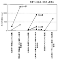
その結果を表1にまとめて示し、この表1の内容をグラフ化して図3に示す。

まず、結晶シリコン基板50がn型の場合を説明する。図3では黒塗りの記号で示す。
希釈フッ酸により自然酸化膜を除去した結晶シリコン基板50の表面(即ち、ベアシリコン表面)のキャリア寿命は20μsであった(比較例4)。これと同じ結晶シリコン基板50に更に上述した水蒸気熱処理を施した後のキャリア寿命は700μsであった(比較例5)。
水蒸気熱処理工程における温度は210℃、水蒸気圧力は1×10⁵ Pa、処理時間は3時間にした。後述する比較例3および実施例1においても同様である。
上記と同様に自然酸化膜を除去した結晶シリコン基板50の表面に、シリコン薄膜52として非晶質シリコン薄膜を形成した場合、その界面のキャリア寿命は、膜厚が3nmのときに27μs、10nmのときに35μs、50nmのときに78μsであった(比較例2)。
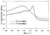
ラマン分光法により、上記膜厚が50nmのシリコン薄膜52のラマン散乱スペクトルを測定したところ、図4中のグラフAに示すように、波数520cm-1近傍の位置に結晶質のシリコンを示すピークは確認できず、波数480cm-1付近に広く拡がる非晶質のシリコンに相当するピークのみが確認できた。
上記比較例2と同じ試料に更に上述した水蒸気熱処理を施した後のキャリア寿命は、膜厚が3nmのときに82μs、10nmのときに250μs、50nmのときに910μsであった(比較例3)。
上記と同様に自然酸化膜を除去した結晶シリコン基板50の表面に、シリコン薄膜52として微結晶シリコン薄膜を50nmの膜厚で形成したところ、その界面のキャリア寿命は250μsであった(比較例1)。
ラマン分光法によって、このシリコン薄膜52のラマン散乱スペクトルを測定したところ、図4中のグラフBに示すように、波数520cm-1近傍の位置に、結晶質のシリコンを示すピークが確認できた。
上記比較例1と同じ試料に更に上述した水蒸気熱処理を施した後のキャリア寿命は1360μsであった(実施例1)。
上記結果から分るように、誘導結合型のプラズマCVD法によって結晶シリコン基板50上に微結晶シリコン薄膜を形成することにより、同じ膜厚でも、非晶質シリコン薄膜を形成した界面のキャリア寿命(78μs)よりも長いキャリア寿命(250μs)を得ることができた。その原因は今のところ良くは分らないが、実験によって上記結果が確かめられた。
更に、実施例1のように誘導結合型のプラズマCVD法による微結晶シリコン薄膜の形成と水蒸気熱処理とを組み合わせることによって、非常に長いキャリア寿命(1360μs)が得られることが確認できた。即ち、ベアシリコン表面と水蒸気熱処理とを組み合わせる場合(比較例5)よりも長く、更に、非晶質シリコン薄膜形成と水蒸気熱処理とを組み合わせる場合(比較例3)よりも長いキャリア寿命を実現することができた。
しかも、前述した界面の水素濃度分布の微妙な制御を必要とする従来技術と違って、結晶シリコン基板上に微結晶シリコン薄膜を形成し、更に水蒸気熱処理を施すという単純なプロセスで、非常に長いキャリア寿命を実現することができた。
次に、結晶シリコン基板50がp型の場合について説明する。図3では白抜きの記号で示す。
上記と同様に自然酸化膜を除去した結晶シリコン基板50の表面に、誘導結合型のプラズマCVD法によってシリコン薄膜52として非晶質シリコン薄膜を10nmの膜厚で形成した場合のキャリア寿命は32μsであり(比較例2)、これと同じ試料に更に水蒸気熱処理を施した後のキャリア寿命は220μsであった(比較例3)。
また、上記と同様に自然酸化膜を除去した結晶シリコン基板50の表面に、誘導結合型のプラズマCVD法によってシリコン薄膜52として微結晶シリコン薄膜を50nmの膜厚で形成した場合のキャリア寿命は58μsであり(比較例1)、これと同じ試料に更に水蒸気熱処理を施した後のキャリア寿命は338μsであった(実施例1)。即ち、この場合も、誘導結合型のプラズマCVD法による微結晶シリコン薄膜の形成と水蒸気熱処理とを組み合わせることによって、長いキャリア寿命を実現することができた。
次に、この発明に係る製造方法を適用することができる太陽電池の構造のより具体的な例を説明する。以下の例は、いずれもハイブリッド型の太陽電池に属するものである。
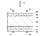
図5に示す太陽電池は、その基本的な構造は良く知られたものであり(例えば特許文献1参照)、結晶シリコン基板50の両面にi型の(即ち、不純物がドープされていない真性の。以下同様)シリコン薄膜54、56を形成し、かつ一方のi型のシリコン薄膜54の表面にp型のシリコン薄膜58を形成し、他方のi型のシリコン薄膜56の表面にn型のシリコン薄膜60を形成した構造を有している。更に、シリコン薄膜58、60の表面に透明導電膜62、64がそれぞれ形成されており、それらの外側表面に光電流を取り出すくし型の電極66、68がそれぞれ形成されている。結晶シリコン基板50は、通常はn型であるが、p型でも良い。光10は、例えば、透明導電膜62側から入射する。
このような構造の太陽電池の製造方法において、例えば、(a)前記薄膜形成工程によって、i型のシリコン薄膜54、56としてi型の前記微結晶シリコン薄膜を形成し、その後前記水蒸気熱処理工程を実行しても良いし、(b)前記薄膜形成工程によって、p型のシリコン薄膜58およびn型のシリコン薄膜60として、p型の前記微結晶シリコン薄膜およびn型の前記微結晶シリコン薄膜をそれぞれ形成し、その後前記水蒸気熱処理工程を実行しても良いし、(c)前記薄膜形成工程によって、i型のシリコン薄膜54、56としてi型の前記微結晶シリコン薄膜を形成し、かつp型のシリコン薄膜58およびn型のシリコン薄膜60として、p型の前記微結晶シリコン薄膜およびn型の前記微結晶シリコン薄膜をそれぞれ形成し、その後前記水蒸気熱処理工程を実行しても良い。なお、この(a)~(c)に記載した以外の膜の形成については、公知の成膜技術を用いれば良い。
ドープされたシリコン薄膜58、60を形成する場合は、前記原料ガス28に、所望のドーパントを含むガスを混合しておけば良い。例えば、p型のシリコン薄膜58を形成する場合はジボラン(B2H6 )を、n型のシリコン薄膜60を形成する場合はホスフィン(PH3 )を、それぞれ適量混合しておけば良い。
結晶シリコン基板50に対する成膜等は、片面ごとに行っても良いし、両面同時に行っても良い。具体的には、成膜等を行う装置の構成等に応じて決めれば良い。
片面ごとに行う場合の全体の製造工程の一例を示すと、結晶シリコン基板50→i型のシリコン薄膜54形成→i型のシリコン薄膜56形成→p型のシリコン薄膜58形成→n型のシリコン薄膜60形成→透明導電膜62形成→透明導電膜64形成→電極66形成→電極68形成→水蒸気熱処理となる。但し、これに限られるものではない。
両面同時に行う場合の全体の製造工程の一例を示すと、結晶シリコン基板50→i型のシリコン薄膜54、56形成→p型のシリコン薄膜58形成→n型のシリコン薄膜60形成→透明導電膜62、64形成→電極66形成→電極68形成→水蒸気熱処理となる。但し、これに限られるものではない。
上記太陽電池におけるi型のシリコン薄膜54、56は、p型またはn型にドープされたシリコン薄膜58、60からの不純物の拡散を防いで界面でのキャリア寿命を延ばすことを主目的とするものであり、上記(a)に示した方法のように、前記薄膜形成工程によって、当該i型のシリコン薄膜54、56としてi型の前記微結晶シリコン薄膜を形成し、その後前記水蒸気熱処理工程を実行することによって、上述したように界面および薄膜中の欠陥を減少させてキャリア寿命を長くすることができるので、i型薄膜54、56の上記主目的をより効果的に達成することができる。
また、背景技術で説明したように、従来はシリコン薄膜58、60としてn型またはp型にドープされた非晶質シリコン薄膜を形成していたのであるが、n型またはp型にドープされた非晶質シリコン薄膜は不純物の活性化率が小さくて低抵抗膜が形成しにくく、低抵抗化するために不純物を増やすとそれが欠陥となってキャリア寿命を短くするという課題がある。これに対して、上記(b)または(c)に示した方法のように、シリコン薄膜58、60としてn型またはp型のドープされた微結晶シリコン薄膜を形成すると、n型またはp型にドープされた微結晶シリコン薄膜は不純物の活性化率が高く、少ない不純物量で低抵抗膜を形成することができる。従って、欠陥形成確率を小さくすることができるので、開放電圧および短絡電流が大きく、変換効率の高い太陽電池を得ることができる。
図6に示す太陽電池は、結晶シリコン基板50の一方の表面にi型のシリコン薄膜74を形成し、当該シリコン薄膜74上に互いに仕事関数の異なる第1の電極76および第2の電極78を形成した構造を有している。両電極76、78は、例えば、くし型をしている。結晶シリコン基板50の他方の表面には、シリコン酸化膜またはシリコン窒化膜等から成る透明保護膜72が形成されている。結晶シリコン基板50は、n型でも良いし、p型でも良い。光10は、この例では透明保護膜72側から入射する。
第1の電極76は、結晶シリコン基板50および第2の電極78の仕事関数よりも小さい仕事関数の金属、例えばアルミニウム(Al )、ハフニウム(Hf )、タンタル(Ta )、インジウム(In )、ジルコニウム(Zr )等の金属で形成されている。第2の電極78は、結晶シリコン基板50および第1の電極76の仕事関数よりも大きい仕事関数の金属、例えば金(Au )、ニッケル(Ni )、白金(Pt )、パラジウム(Pd )等の金属で形成されている。
この太陽電池は、電極76、シリコン薄膜74および結晶シリコン基板50でMIS(金属/絶縁薄膜/半導体)構造が形成され、更に電極78、シリコン薄膜74および結晶シリコン基板50でもMIS構造が形成されていて、ダブルMIS構造となっており、これと上記電極76、78の仕事関数差を利用することにより、効率良く発電することができる。
このような構造の太陽電池の製造において、前記薄膜形成工程によって、i型のシリコン薄膜74としてi型の前記微結晶シリコン薄膜を形成し、その後前記水蒸気熱処理工程を実行する。なお、透明保護膜72の形成については、公知の成膜技術を用いれば良い。
この太陽電池の全体の製造工程の一例を示すと、結晶シリコン基板50→透明保護膜72形成→結晶シリコン基板50の下面(シリコン薄膜74側の表面)の酸化膜除去→シリコン薄膜74形成→電極76形成→電極78形成→水蒸気熱処理となる。但し、これに限られるものではない。
このような構造を有する太陽電池の製造において、前記薄膜形成工程によって、i型のシリコン薄膜74としてi型の前記微結晶シリコン薄膜を形成し、その後前記水蒸気熱処理工程を実行することによって、上述したように界面および薄膜中の欠陥を減少させて長いキャリア寿命を実現することができるので、より変換効率の高い太陽電池を得ることができる。
上述した各製造方法によって製造された太陽電池は、上述した理由によって、高い変換効率を実現することができる。
50 結晶シリコン基板
52 シリコン薄膜
54、56 i型のシリコン薄膜
58 p型のシリコン薄膜
60 n型のシリコン薄膜
74 i型のシリコン薄膜
52 シリコン薄膜
54、56 i型のシリコン薄膜
58 p型のシリコン薄膜
60 n型のシリコン薄膜
74 i型のシリコン薄膜
Claims (8)
- 結晶シリコン基板上にシリコン薄膜を形成した構造を有する太陽電池の製造方法であって、
誘導結合によってプラズマを生成する誘導結合型のプラズマCVD法によって、前記結晶シリコン基板上に、前記シリコン薄膜として、微小なシリコン結晶を含む微結晶シリコン薄膜を形成する薄膜形成工程と、
前記結晶シリコン基板上に前記微結晶シリコン薄膜を形成したものに、5×10⁵ Pa以上の圧力の水蒸気雰囲気中で熱処理を施す水蒸気熱処理工程とを備えている、ことを特徴とする太陽電池の製造方法。 - 前記薄膜形成工程における前記結晶シリコン基板の温度を100℃~300℃にする請求項1記載の太陽電池の製造方法。
- 前記水蒸気熱処理工程における温度を150℃~300℃、水蒸気圧力を5×10⁵ Pa~1.5×10⁶ Pa、処理時間を0.5時間~3時間にする請求項1または2記載の太陽電池の製造方法。
- 前記太陽電池は、結晶シリコン基板の両面にi型のシリコン薄膜を形成し、かつ一方のi型のシリコン薄膜の表面にp型のシリコン薄膜を形成し、他方のi型のシリコン薄膜の表面にn型のシリコン薄膜を形成した構造を有するものであり、
前記薄膜形成工程によって、前記i型のシリコン薄膜としてi型の前記微結晶シリコン薄膜を形成し、
その後前記水蒸気熱処理工程を実行する請求項1、2または3記載の太陽電池の製造方法。 - 前記太陽電池は、結晶シリコン基板の両面にi型のシリコン薄膜を形成し、かつ一方のi型のシリコン薄膜の表面にp型のシリコン薄膜を形成し、他方のi型のシリコン薄膜の表面にn型のシリコン薄膜を形成した構造を有するものであり、
前記薄膜形成工程によって、前記p型のシリコン薄膜およびn型のシリコン薄膜として、p型の前記微結晶シリコン薄膜およびn型の前記微結晶シリコン薄膜をそれぞれ形成し、
その後前記水蒸気熱処理工程を実行する請求項1、2または3記載の太陽電池の製造方法。 - 前記太陽電池は、結晶シリコン基板の両面にi型のシリコン薄膜を形成し、かつ一方のi型のシリコン薄膜の表面にp型のシリコン薄膜を形成し、他方のi型のシリコン薄膜の表面にn型のシリコン薄膜を形成した構造を有するものであり、
前記薄膜形成工程によって、前記i型のシリコン薄膜としてi型の前記微結晶シリコン薄膜を形成し、かつ前記p型のシリコン薄膜およびn型のシリコン薄膜として、p型の前記微結晶シリコン薄膜およびn型の前記微結晶シリコン薄膜をそれぞれ形成し、
その後前記水蒸気熱処理工程を実行する請求項1、2または3記載の太陽電池の製造方法。 - 前記太陽電池は、結晶シリコン基板上にi型のシリコン薄膜を形成し、当該シリコン薄膜上に互いに仕事関数の異なる第1および第2の電極を形成した構造を有するものであり、
前記薄膜形成工程によって、前記i型のシリコン薄膜としてi型の前記微結晶シリコン薄膜を形成し、
その後前記水蒸気熱処理工程を実行する請求項1、2または3記載の太陽電池の製造方法。 - 請求項1から7のいずれか一項に記載の製造方法によって製造された太陽電池。
Priority Applications (2)
| Application Number | Priority Date | Filing Date | Title |
|---|---|---|---|
| US14/131,205 US20140144495A1 (en) | 2011-07-11 | 2012-02-03 | Solar cell and method for manufacturing the same |
| CN201280034187.6A CN103688371A (zh) | 2011-07-11 | 2012-02-03 | 太阳能电池及其制造方法 |
Applications Claiming Priority (2)
| Application Number | Priority Date | Filing Date | Title |
|---|---|---|---|
| JP2011-152562 | 2011-07-11 | ||
| JP2011152562A JP5773194B2 (ja) | 2011-07-11 | 2011-07-11 | 太陽電池の製造方法 |
Publications (1)
| Publication Number | Publication Date |
|---|---|
| WO2013008482A1 true WO2013008482A1 (ja) | 2013-01-17 |
Family
ID=47505783
Family Applications (1)
| Application Number | Title | Priority Date | Filing Date |
|---|---|---|---|
| PCT/JP2012/052464 Ceased WO2013008482A1 (ja) | 2011-07-11 | 2012-02-03 | 太陽電池およびその製造方法 |
Country Status (4)
| Country | Link |
|---|---|
| US (1) | US20140144495A1 (ja) |
| JP (1) | JP5773194B2 (ja) |
| CN (1) | CN103688371A (ja) |
| WO (1) | WO2013008482A1 (ja) |
Families Citing this family (5)
| Publication number | Priority date | Publication date | Assignee | Title |
|---|---|---|---|---|
| US20150380581A1 (en) * | 2014-06-27 | 2015-12-31 | Michael C. Johnson | Passivation of light-receiving surfaces of solar cells with crystalline silicon |
| JP2017045767A (ja) * | 2015-08-24 | 2017-03-02 | 学校法人トヨタ学園 | 光電変換素子およびその製造方法 |
| JP2017107947A (ja) * | 2015-12-08 | 2017-06-15 | 国立大学法人 琉球大学 | 半導体装置、電子機器、及び、半導体装置の製造方法 |
| KR102018381B1 (ko) * | 2017-01-26 | 2019-09-04 | 엘지전자 주식회사 | 태양 전지 및 이의 제조 방법 |
| SG11202008981TA (en) | 2018-03-28 | 2020-10-29 | Applied Materials Inc | Remote capacitively coupled plasma deposition of amorphous silicon |
Citations (5)
| Publication number | Priority date | Publication date | Assignee | Title |
|---|---|---|---|---|
| JP2003298078A (ja) * | 2002-03-29 | 2003-10-17 | Ebara Corp | 光起電力素子 |
| JP2006319335A (ja) * | 2005-05-12 | 2006-11-24 | General Electric Co <Ge> | 表面パシベーティッド光起電装置 |
| JP2007281156A (ja) * | 2006-04-06 | 2007-10-25 | Japan Advanced Institute Of Science & Technology Hokuriku | 裏面電極型半導体へテロ接合太陽電池ならびにその製造方法と製造装置 |
| JP2008519438A (ja) * | 2004-10-29 | 2008-06-05 | ビーピー・コーポレーション・ノース・アメリカ・インコーポレーテッド | バックコンタクト太陽電池 |
| JP2010258102A (ja) * | 2009-04-22 | 2010-11-11 | Serubakku:Kk | 光電変換デバイスの製造方法、光電変換デバイス製造装置および光電変換デバイス |
Family Cites Families (6)
| Publication number | Priority date | Publication date | Assignee | Title |
|---|---|---|---|---|
| CA918297A (en) * | 1969-09-24 | 1973-01-02 | Tanimura Shigeru | Semiconductor device and method of making |
| JP5309426B2 (ja) * | 2006-03-29 | 2013-10-09 | 株式会社Ihi | 微結晶シリコン膜形成方法及び太陽電池 |
| JP2009135277A (ja) * | 2007-11-30 | 2009-06-18 | Tokyo Electron Ltd | 膜の形成方法、薄膜トランジスタ、太陽電池、製造装置および表示装置 |
| EP2261995B1 (en) * | 2008-03-19 | 2019-05-22 | Panasonic Intellectual Property Management Co., Ltd. | Solar cell and method for manufacturing the same |
| EP2105972A3 (en) * | 2008-03-28 | 2015-06-10 | Semiconductor Energy Laboratory Co, Ltd. | Photoelectric conversion device and method for manufacturing the same |
| JP2010205804A (ja) * | 2009-02-27 | 2010-09-16 | Mitsubishi Heavy Ind Ltd | 光電変換装置 |
-
2011
- 2011-07-11 JP JP2011152562A patent/JP5773194B2/ja active Active
-
2012
- 2012-02-03 WO PCT/JP2012/052464 patent/WO2013008482A1/ja not_active Ceased
- 2012-02-03 CN CN201280034187.6A patent/CN103688371A/zh active Pending
- 2012-02-03 US US14/131,205 patent/US20140144495A1/en not_active Abandoned
Patent Citations (5)
| Publication number | Priority date | Publication date | Assignee | Title |
|---|---|---|---|---|
| JP2003298078A (ja) * | 2002-03-29 | 2003-10-17 | Ebara Corp | 光起電力素子 |
| JP2008519438A (ja) * | 2004-10-29 | 2008-06-05 | ビーピー・コーポレーション・ノース・アメリカ・インコーポレーテッド | バックコンタクト太陽電池 |
| JP2006319335A (ja) * | 2005-05-12 | 2006-11-24 | General Electric Co <Ge> | 表面パシベーティッド光起電装置 |
| JP2007281156A (ja) * | 2006-04-06 | 2007-10-25 | Japan Advanced Institute Of Science & Technology Hokuriku | 裏面電極型半導体へテロ接合太陽電池ならびにその製造方法と製造装置 |
| JP2010258102A (ja) * | 2009-04-22 | 2010-11-11 | Serubakku:Kk | 光電変換デバイスの製造方法、光電変換デバイス製造装置および光電変換デバイス |
Non-Patent Citations (2)
| Title |
|---|
| MASAHIKO HASUMI ET AL.: "Defect Reduction of Commercial Solar Cells by High-Pressure H_20 Vapor Treatment", PROCEEDINGS OF THE SYMPOSIUM ON SEMICONDUCTORS AND INTEGRATED CIRCUITS TECHNOLOGY, vol. 73, 9 July 2009 (2009-07-09), pages 37 - 40 * |
| YUICHI NAGAO ET AL.: "Amorphous Silicon Seimaku to Koatsu Suijoki Netsushori ni yoru Kessho Silicon Hyomen Passivation", DAI 58 KAI EXTENDED ABSTRACTS, 9 March 2011 (2011-03-09), pages 25A - BK-8 * |
Also Published As
| Publication number | Publication date |
|---|---|
| JP2013021095A (ja) | 2013-01-31 |
| US20140144495A1 (en) | 2014-05-29 |
| CN103688371A (zh) | 2014-03-26 |
| JP5773194B2 (ja) | 2015-09-02 |
Similar Documents
| Publication | Publication Date | Title |
|---|---|---|
| Sharma et al. | Nanocrystalline silicon thin film growth and application for silicon heterojunction solar cells: a short review | |
| CN105762234B (zh) | 一种隧穿氧化层钝化接触太阳能电池及其制备方法 | |
| JP4797083B2 (ja) | 薄膜太陽電池モジュール | |
| CN103119727B (zh) | 光电转换装置的制造方法 | |
| CN101573782A (zh) | 半导体层的制造方法和半导体层制造装置以及使用它们制造的半导体器件 | |
| JP4411338B2 (ja) | 薄膜太陽電池モジュール | |
| CN101395721B (zh) | 光电转换装置及其制造方法 | |
| JPWO2003085746A1 (ja) | タンデム型薄膜光電変換装置の製造方法 | |
| CN104617165B (zh) | 一种二硫化钼/缓冲层/硅n-i-p太阳能电池器件及其制备方法 | |
| JP5773194B2 (ja) | 太陽電池の製造方法 | |
| CN117276359A (zh) | 一种隧穿氧化多层结构及其制备方法与应用 | |
| CN108475707A (zh) | 光电转换装置的制造方法 | |
| Bhattacharya et al. | Development of high conducting phosphorous doped nanocrystalline thin silicon films for silicon heterojunction solar cells application | |
| JP4758496B2 (ja) | 薄膜太陽電池モジュール | |
| Lien et al. | Deposition and characterization of high-efficiency silicon thin-film solar cells by HF-PECVD and OES technology | |
| TWI790245B (zh) | 光電轉換裝置之製造方法 | |
| CN102856438B (zh) | 一种提高太阳能电池表面钝化的方法 | |
| CN113437183A (zh) | 一种pecvd沉积非晶硅薄膜的方法 | |
| JP2007258537A (ja) | 光電変換装置及びその製造方法 | |
| JP5770294B2 (ja) | 光電変換装置およびその製造方法 | |
| JP4758495B2 (ja) | 薄膜太陽電池モジュール | |
| Zhang et al. | Micromorph tandem solar cells: optimization of the microcrystalline silicon bottom cell in a single chamber system | |
| JP2009004702A (ja) | 光電変換装置の製造方法 | |
| JP2003142712A (ja) | 太陽電池の製造方法および太陽電池 | |
| EP2192620A1 (en) | Photoelectric conversion apparatus and method for manufacturing the same |
Legal Events
| Date | Code | Title | Description |
|---|---|---|---|
| 121 | Ep: the epo has been informed by wipo that ep was designated in this application |
Ref document number: 12810552 Country of ref document: EP Kind code of ref document: A1 |
|
| WWE | Wipo information: entry into national phase |
Ref document number: 14131205 Country of ref document: US |
|
| NENP | Non-entry into the national phase |
Ref country code: DE |
|
| 122 | Ep: pct application non-entry in european phase |
Ref document number: 12810552 Country of ref document: EP Kind code of ref document: A1 |