WO2012176838A1 - 太陽電池および太陽電池の製造方法 - Google Patents
太陽電池および太陽電池の製造方法 Download PDFInfo
- Publication number
- WO2012176838A1 WO2012176838A1 PCT/JP2012/065863 JP2012065863W WO2012176838A1 WO 2012176838 A1 WO2012176838 A1 WO 2012176838A1 JP 2012065863 W JP2012065863 W JP 2012065863W WO 2012176838 A1 WO2012176838 A1 WO 2012176838A1
- Authority
- WO
- WIPO (PCT)
- Prior art keywords
- silicon substrate
- back surface
- solar cell
- type silicon
- uneven shape
- Prior art date
- Legal status (The legal status is an assumption and is not a legal conclusion. Google has not performed a legal analysis and makes no representation as to the accuracy of the status listed.)
- Ceased
Links
Images


Classifications
-
- H—ELECTRICITY
- H10—SEMICONDUCTOR DEVICES; ELECTRIC SOLID-STATE DEVICES NOT OTHERWISE PROVIDED FOR
- H10F—INORGANIC SEMICONDUCTOR DEVICES SENSITIVE TO INFRARED RADIATION, LIGHT, ELECTROMAGNETIC RADIATION OF SHORTER WAVELENGTH OR CORPUSCULAR RADIATION
- H10F71/00—Manufacture or treatment of devices covered by this subclass
- H10F71/121—The active layers comprising only Group IV materials
-
- H—ELECTRICITY
- H10—SEMICONDUCTOR DEVICES; ELECTRIC SOLID-STATE DEVICES NOT OTHERWISE PROVIDED FOR
- H10F—INORGANIC SEMICONDUCTOR DEVICES SENSITIVE TO INFRARED RADIATION, LIGHT, ELECTROMAGNETIC RADIATION OF SHORTER WAVELENGTH OR CORPUSCULAR RADIATION
- H10F10/00—Individual photovoltaic cells, e.g. solar cells
- H10F10/10—Individual photovoltaic cells, e.g. solar cells having potential barriers
- H10F10/14—Photovoltaic cells having only PN homojunction potential barriers
-
- H—ELECTRICITY
- H10—SEMICONDUCTOR DEVICES; ELECTRIC SOLID-STATE DEVICES NOT OTHERWISE PROVIDED FOR
- H10F—INORGANIC SEMICONDUCTOR DEVICES SENSITIVE TO INFRARED RADIATION, LIGHT, ELECTROMAGNETIC RADIATION OF SHORTER WAVELENGTH OR CORPUSCULAR RADIATION
- H10F77/00—Constructional details of devices covered by this subclass
- H10F77/20—Electrodes
- H10F77/206—Electrodes for devices having potential barriers
- H10F77/211—Electrodes for devices having potential barriers for photovoltaic cells
-
- H—ELECTRICITY
- H10—SEMICONDUCTOR DEVICES; ELECTRIC SOLID-STATE DEVICES NOT OTHERWISE PROVIDED FOR
- H10F—INORGANIC SEMICONDUCTOR DEVICES SENSITIVE TO INFRARED RADIATION, LIGHT, ELECTROMAGNETIC RADIATION OF SHORTER WAVELENGTH OR CORPUSCULAR RADIATION
- H10F77/00—Constructional details of devices covered by this subclass
- H10F77/70—Surface textures, e.g. pyramid structures
- H10F77/703—Surface textures, e.g. pyramid structures of the semiconductor bodies, e.g. textured active layers
-
- Y—GENERAL TAGGING OF NEW TECHNOLOGICAL DEVELOPMENTS; GENERAL TAGGING OF CROSS-SECTIONAL TECHNOLOGIES SPANNING OVER SEVERAL SECTIONS OF THE IPC; TECHNICAL SUBJECTS COVERED BY FORMER USPC CROSS-REFERENCE ART COLLECTIONS [XRACs] AND DIGESTS
- Y02—TECHNOLOGIES OR APPLICATIONS FOR MITIGATION OR ADAPTATION AGAINST CLIMATE CHANGE
- Y02E—REDUCTION OF GREENHOUSE GAS [GHG] EMISSIONS, RELATED TO ENERGY GENERATION, TRANSMISSION OR DISTRIBUTION
- Y02E10/00—Energy generation through renewable energy sources
- Y02E10/50—Photovoltaic [PV] energy
- Y02E10/547—Monocrystalline silicon PV cells
-
- Y—GENERAL TAGGING OF NEW TECHNOLOGICAL DEVELOPMENTS; GENERAL TAGGING OF CROSS-SECTIONAL TECHNOLOGIES SPANNING OVER SEVERAL SECTIONS OF THE IPC; TECHNICAL SUBJECTS COVERED BY FORMER USPC CROSS-REFERENCE ART COLLECTIONS [XRACs] AND DIGESTS
- Y02—TECHNOLOGIES OR APPLICATIONS FOR MITIGATION OR ADAPTATION AGAINST CLIMATE CHANGE
- Y02P—CLIMATE CHANGE MITIGATION TECHNOLOGIES IN THE PRODUCTION OR PROCESSING OF GOODS
- Y02P70/00—Climate change mitigation technologies in the production process for final industrial or consumer products
- Y02P70/50—Manufacturing or production processes characterised by the final manufactured product
Definitions
- the present invention relates to a solar cell and a method for manufacturing a solar cell, and more particularly to a structure of a surface of a solar cell (back surface of a solar cell) located on the side opposite to a side on which light is incident.
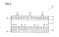
- FIG. 4 is a cross-sectional view schematically showing an example of the configuration of the solar cell 21 disclosed in Patent Document 1 (Japanese Patent Laid-Open No. 9-237910).
- an n-type silicon semiconductor layer 12 is provided on a surface of the p-type silicon semiconductor substrate 11 that is positioned on the light incident side (hereinafter referred to as “light-receiving surface of the p-type silicon semiconductor substrate 11”).
- the n-type silicon semiconductor layer 12 is covered with a silicon oxide film layer 13, and the silicon oxide film layer 13 is covered with an antireflection film layer 14.
- the grid electrode 15 passes through the antireflection film layer 14 and the silicon oxide film layer 13 and is connected to the n-type silicon semiconductor layer 12.
- the surface opposite to the light receiving surface of the p-type silicon semiconductor substrate 11 (hereinafter referred to as “the back surface of the p-type silicon semiconductor substrate 11”) is covered with the silicon oxide film layer 16, and the silicon oxide film layer 16 is hydrogenated.
- the silicon nitride film layer 17 is covered.
- a p + -type microcrystalline silicon semiconductor layer 18 which is a high-concentration p-type semiconductor layer covers the hydrogenated silicon nitride film layer 17 and includes a plurality of portions of the hydrogenated silicon nitride film layer 17 and the silicon oxide film layer 16. And is connected to the back surface of the p-type silicon semiconductor substrate 11.
- the p + type microcrystalline silicon semiconductor layer 18 is covered with a back electrode 19.
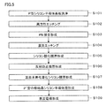
- FIG. 5 is a flowchart showing an example of a method for manufacturing a solar cell disclosed in Patent Document 1.
- Patent Document 1 describes a method for manufacturing a solar cell described below as an example.
- the p-type silicon semiconductor substrate 11 is cleaned in a p-type silicon semiconductor substrate cleaning step (S101. “S” represents a step. The same applies hereinafter).
- S102 anisotropic etching is performed so that the surface of the p-type silicon semiconductor substrate 11 becomes uneven.
- the pn junction forming step (S103) phosphorus is diffused by vapor phase diffusion using POCl 3 to form the n-type silicon semiconductor layer 12.
- the back surface etching step (S104) the back surface side of the p-type silicon semiconductor substrate 11 is etched to remove the n-type silicon semiconductor layer formed on the back surface.
- the silicon oxide film layer forming step (S105) the silicon oxide film layer 13 and the silicon oxide film layer 16 are formed by a thermal oxidation method.
- an antireflection film layer 14 made of a silicon nitride film is formed by a plasma CVD method.
- a silicon hydronitride film layer 17 is formed on the silicon oxide film layer 16 in the backside hydrogenated silicon nitride film layer forming step (S107).
- the silicon hydronitride film layer 17 and the silicon oxide film layer 16 are processed by using a photoetching method. Thereafter, a p + type microcrystalline silicon semiconductor layer 18 is formed by plasma CVD so as to cover the hydrogenated silicon nitride film layer 17 and the silicon oxide film layer 16.
- the back electrode 19 is formed so as to cover the p + type microcrystalline silicon semiconductor layer 18 by vapor deposition.
- the grid electrode 15 is formed by a vapor deposition method. In this way, the solar cell 21 is manufactured.
- texture structure is unevenness formed by anisotropic etching
- a wet etching method is often used in a production line. ing.
- irregularities are formed on the entire surface of the p-type silicon semiconductor substrate (not only on the light receiving surface but also on the back surface and the end surface).
- the surface area of the back surface of the p-type silicon semiconductor substrate is larger than in the state where the uneven shape is not formed on the back surface of the p-type silicon semiconductor substrate. Become. Therefore, since the number of dangling bonds existing on the back surface of the p-type silicon semiconductor substrate increases, carrier recombination increases. As a result, the solar cell characteristics are adversely affected. This is also true when an n-type silicon semiconductor substrate is used as the silicon semiconductor substrate.
- the present invention has been made in view of the above problems, and an object of the present invention is to optimize the size of the concavo-convex shape on the back surface side in a solar cell having a concavo-convex shape on each of the light receiving surface and the back surface of the silicon substrate. This is to improve the solar cell characteristics.
- a solar cell includes a first conductivity type silicon substrate, a light receiving surface side uneven shape formed on the light receiving surface of the silicon substrate, a second conductivity type semiconductor layer formed on the light receiving surface of the silicon substrate, A back side uneven shape formed on the back side of the silicon substrate; a light receiving side electrode formed on a part of the light receiving surface of the silicon substrate; and a back side electrode formed on a part of the back side of the silicon substrate; Is provided.
- the plane area of the back surface of the silicon substrate is S
- the surface area of the concavo-convex shape of the silicon substrate is X
- the surface area ratio Y is 1.05 or more and 1.15 or less. It is.
- the back surface side uneven shape of the silicon substrate may be smaller than the light receiving surface side uneven shape of the silicon substrate.
- a back surface side electrode may consist of aluminum.
- the method for manufacturing a solar cell according to the present invention includes a step of forming a textured structure on a first conductivity type silicon substrate, and thermally diffusing a second conductivity type dopant on the silicon substrate, thereby forming a first on the light receiving surface of the silicon substrate.
- the back surface side uneven shape is made smaller than the light receiving surface side uneven shape formed on the light receiving surface of the silicon substrate.
- the solar cell characteristics are improved.
- FIG. 1 is a cross-sectional view schematically showing an example of the configuration of the solar cell of the present invention.
- first conductivity type and second conductivity type in the claims are “p-type” and “n-type”, respectively, will be described.
- present invention includes a case where the “first conductivity type” and the “second conductivity type” in the claims are “n-type” and “p-type”, respectively.
- the surface of the p-type silicon substrate 2 on the light incident side (hereinafter referred to as “light-receiving surface of the p-type silicon substrate 2”) is n-type such as phosphorus.
- the n-type semiconductor layer 3 is formed by a thermal diffusion method using a dopant.
- the thickness of the n-type semiconductor layer 3 is preferably about 0.3 ⁇ m. Thereby, a pn junction is formed at the interface between the p-type silicon substrate 2 and the n-type semiconductor layer 3.
- a light receiving surface side electrode 4 which is a comb-like metal electrode is provided on the light receiving surface of the p-type silicon substrate 2.
- the light receiving surface side electrode 4 is preferably made of, for example, silver.
- a light receiving surface side uneven shape 6 having a texture structure is formed on the light receiving surface of the p-type silicon substrate 2.
- an antireflection film 7 is formed on the light receiving surface side uneven shape 6, an antireflection film 7 is formed.
- the antireflection film 7 is preferably a silicon nitride film, for example.
- the light-receiving surface side electrode 4 is provided in a through-hole formed by patterning or fire-through the antireflection film 7, thereby contacting the n-type semiconductor layer 3.
- a back-side electrode 5 is formed on the surface opposite to the light receiving surface of the p-type silicon substrate 2 (hereinafter referred to as “the back surface of the p-type silicon substrate 2”).
- the back surface side electrode 5 is preferably made of, for example, aluminum.
- the thickness of the back surface side electrode 5 is preferably 0.4 ⁇ m or more and 8 ⁇ m or less, for example.
- a patterned back surface side field layer 8 (BSF (Back Surface Field) layer) is formed on the back surface of the p-type silicon substrate 2, and a passivation film 9 is formed on the back surface of the p-type silicon substrate 2. .
- BSF Back Surface Field
- the back side electric field layer 8 is preferably a diffusion layer formed by diffusing aluminum or the like, for example, and the thickness of the back side electric field layer 8 is preferably, for example, 1 ⁇ m or more.
- the passivation film 9 is preferably a silicon nitride film, for example, and the thickness of the passivation film 9 is preferably 0.06 ⁇ m or more and 0.75 ⁇ m or less, for example.
- a back surface-side uneven shape 10 is formed on the back surface of the p-type silicon substrate 2.
- the light-receiving surface side uneven shape 6 and the back surface-side uneven shape 10 are only schematically described, and the light-receiving surface side uneven shape 6 and the back surface-side uneven shape 10 are actually random uneven shapes. It is.
- the plane area of the back surface of the p-type silicon substrate 2 is S
- the surface area of the back-side uneven shape 10 of the p-type silicon substrate 2 is X
- the surface area ratio Y is 1.05 or more and 1.15 or less.
- the surface area ratio Y is 1.0 when the irregular shape is not formed on the back surface of the p-type silicon substrate.
- the plane area of the back surface of the p-type silicon substrate 2 is the surface area of the back surface of the p-type silicon substrate 2 in a state in which no concavo-convex shape is formed.
- the surface area of the concavo-convex shape 10 on the back surface side of the p-type silicon substrate 2 is the surface area of the back surface when the concavo-convex shape is formed on the back surface of the p-type silicon substrate 2. It is calculated using etc.
- the surface area ratio Y is less than 1.05, the adhesion strength of the light-receiving surface side electrode to the back surface of the p-type silicon substrate is reduced. For this reason, the curve factor and the like are reduced.
- the surface area ratio Y exceeds 1.15, the number of dangling bonds existing on the back surface of the p-type silicon substrate is increased, so that the recombination of carriers is increased, and thus the photoelectric conversion efficiency is decreased. .
- the surface area ratio Y is 1.05 or more and 1.15 or less, the adhesion strength of the light-receiving surface side electrode 4 to the back surface of the p-type silicon substrate 2 is ensured, and the surface area ratio Y exists on the back surface of the p-type silicon substrate 2. Increase in the number of dangling bonds can be prevented. Therefore, solar cell characteristics such as a fill factor and photoelectric conversion efficiency are improved.
- the back surface side uneven shape 10 is preferably smaller than the light receiving surface side uneven shape 6.
- the uneven shape is small means that the height difference is small. If the size of the back surface unevenness is greater than the size of the light receiving surface side uneven shape, the number of dangling bonds present on the back surface of the p-type silicon substrate may be excessive. However, if the back-side uneven shape 10 is smaller than the light-receiving surface-side uneven shape 6, the number of dangling bonds existing on the back surface of the p-type silicon substrate 2 is optimized, so that the photoelectric conversion efficiency and the like are improved.
- FIG. 2 is a flowchart showing an example of a method for manufacturing the solar cell shown in FIG.
- the entire surface of the p-type silicon substrate 2 that is, a surface that serves as a light-receiving surface of the p-type silicon substrate 2 (hereinafter referred to as “p-type silicon substrate”). 2), a surface to be the back surface of the p-type silicon substrate 2 (hereinafter referred to as “the back surface of the p-type silicon substrate 2”) and an end surface of the p-type silicon substrate 2 by a wet etching method.
- a wet etching method an acidic solution or an alkaline solution can be used.
- the light receiving surface side uneven shape 6 is formed on the light receiving surface of the p-type silicon substrate 2.
- the n-type semiconductor layer 3 is formed on the light receiving surface of the p-type silicon substrate 2.
- a pn junction is formed at the interface between the p-type silicon substrate 2 and the n-type semiconductor layer 3.
- a PSG (phosphosilicate glass) layer which is a glass layer is formed on the n-type semiconductor layer 3 when the n-type semiconductor layer 3 is formed, for example, dilute hydrofluoric acid is used after the n-type semiconductor layer 3 is formed. It is preferable to remove the PSG layer.
- a thermal diffusion method using a gas containing an n-type dopant can be used as a method for forming the n-type semiconductor layer 3.
- a gas containing an n-type dopant as a diffusion material
- the p-type silicon substrate 2 is heat-treated at a temperature of 800 ° C. or higher in a tube furnace.
- the n-type dopant is vapor-phase diffused, and the n-type semiconductor layer 3 is formed on the entire surface of the p-type silicon substrate 2.
- POCl 3 or the like can be used as the gas containing the n-type dopant.
- the n-type semiconductor layer 3 may be formed not only on the light-receiving surface of the p-type silicon substrate 2 but also on the back surface and end surface of the p-type silicon substrate 2, but is formed on the back surface and end surface of the p-type silicon substrate 2.
- the n-type semiconductor layer 3 is removed by etching in a back surface etching step (S4) described later.
- the n-type semiconductor layer 3 is not formed by a thermal diffusion method, but by a coating diffusion method in which a solution containing an n-type dopant (for example, PSG liquid) is applied to the light-receiving surface of the p-type silicon substrate 2 and then heat treatment is performed. Can also be used.
- a solution containing an n-type dopant for example, PSG liquid
- an antireflection film 7 is formed on the n-type semiconductor layer 3 in the antireflection film formation step (S3).
- a silicon nitride film is used as the antireflection film 7, it is preferable to form the antireflection film 7 having a thickness of about 70 nm by a plasma CVD method using silane and ammonia as gas species.
- the back surface etching step (S4) the back surface of the p-type silicon substrate 2 is etched. As a result, a back surface-side uneven shape 10 is formed on the back surface of the p-type silicon substrate 2.
- a protective tape for preventing etching is applied to the light receiving surface of the p-type silicon substrate 2.
- the material of the protective tape is not particularly limited, but preferably has resistance to an etching solution used in etching in the next step. Since an acidic solution is used as the etching solution in the next step, the protective tape preferably has acid resistance.
- the back surface of the p-type silicon substrate 2 is wet etched. As a result, the n-type semiconductor layer 3 formed on the back surface of the p-type silicon substrate 2 is removed, and a back-side uneven shape 10 is formed on the back surface of the p-type silicon substrate 2. Further, the n-type semiconductor layer 3 formed on the end face of the p-type silicon substrate 2 is also removed.
- the back side uneven shape 10 is formed by smoothing the texture structure formed on the back side of the p-type silicon substrate 2 in the texturing step (S1) (reducing the height difference of the texture structure) by this step. The Therefore, if this step is performed, the surface area of the back surface of the p-type silicon substrate 2 is reduced, and the number of dangling bonds existing on the back surface of the p-type silicon substrate 2 is reduced. Therefore, when the back surface-side uneven shape 10 is formed, the surface area of the back surface of the p-type silicon substrate 2 is smaller than when the texture structure remains on the back surface of the p-type silicon substrate. The number of dangling bonds decreases.
- the back side uneven shape 10 is smaller than the light receiving surface side uneven shape 6. It is preferable to form the back side uneven shape 10 so that the surface area ratio Y is 1.05 or more and 1.15 or less. Thereby, the solar cell excellent in solar cell characteristics, such as a fill factor and photoelectric conversion efficiency, can be manufactured.
- the wet etching conditions in this step are not particularly limited.
- a mixed solution of hydrofluoric acid (HF) and nitric acid (HNO 3 ) as an etching solution.
- the time for immersing the p-type silicon substrate 2 in the etching solution is preferably 5 seconds or more.
- the solar cell excellent in solar cell characteristics such as a curve factor and photoelectric conversion efficiency, can be manufactured.
- the immersion time is less than 5 seconds, the texture structure formed on the back surface of the p-type silicon substrate 2 in the texturing step (S1) may not be smoothed (the difference in height of the texture structure may be reduced). is there. Therefore, the number of dangling bonds existing on the back surface of the p-type silicon substrate 2 may be increased.
- the immersion time is too long, the texture structure formed on the back surface of the p-type silicon substrate 2 in the texturing step (S1) may be completely removed, and the back surface uneven shape may not be formed. is there.
- the etching solution is preferably 10 ° C. or higher and 40 ° C. or lower.
- the silicon oxide film remaining on the back surface of the p-type silicon substrate 2 is removed using, for example, dilute hydrofluoric acid, and then the passivation film 9 is formed by, for example, plasma CVD. It is formed on the back side uneven shape 10.
- a silicon nitride film is preferably formed as the passivation film 9.
- the passivation film 9 is etched into a back-side electric field layer pattern having a predetermined shape by, for example, a photolithography method to form a contact hole penetrating the passivation film 9.
- an aluminum paste made of aluminum powder, glass frit, resin, organic solvent, etc. is printed on the patterned passivation film 9 by, for example, a screen printing method or the like.
- the p-type silicon substrate 2 is fired at 700 ° C. or higher.
- aluminum diffuses on the back side of the p-type silicon substrate 2 at the location corresponding to the contact hole, and the back side electric field layer 8 made of an aluminum diffusion layer is formed.
- aluminum remaining on the back surface of the p-type silicon substrate 2 is removed with, for example, hydrochloric acid.
- a metal such as aluminum is vapor-deposited on the patterned passivation film 9 by, for example, a vacuum vapor deposition method or the like. Thereby, the back surface side electrode 5 is formed. At this time, a metal such as aluminum is deposited and filled in the contact hole.
- a silver paste made of silver powder, glass frit, resin, organic solvent, etc. is printed on the antireflection film 7 by, for example, screen printing.
- the p-type silicon substrate 2 is baked at 500 ° C. or higher.
- the light-receiving surface side electrode 4 made of silver is formed.
- the light-receiving surface side electrode 4 is formed by the silver paste breaking through the antireflection film 7 when the p-type silicon substrate 2 is baked, that is, the silver paste is formed by fire-through the antireflection film 7.
- the light receiving surface side electrode 4 is electrically connected to the n-type semiconductor layer 3.
- the solar cell 1 shown in FIG. 1 is manufactured.
- the material of the component of the solar cell 1 is not limited to the said description. Further, the thickness of the constituent elements of the solar cell 1 is not limited to the above description.
- a solar cell was manufactured according to the manufacturing method of the solar cell 1 shown in FIG. 2 using a 100-mm square p-type silicon substrate having a thickness of 100 to 200 ⁇ m.
- the etching time time for immersing the n-type silicon substrate in the etching solution
- the back surface etching step S4
- the size of the back side uneven shape is changed, and the solar cell characteristics of the manufactured solar cell are changed.
- the size of the back surface side uneven shape 10 was evaluated.
- the surface area ratio Y was determined using the following formula (1).
- S in the following formula (1) is the plane area of the back surface of the p-type silicon substrate
- X is the surface area of the concavo-convex shape of the back surface of the p-type silicon substrate. S ... Formula (1).
- the surface area of the concavo-convex shape on the back side of the p-type silicon substrate is obtained using a laser microscope (wavelength: 408 nm) and a confocal laser scanning microscope (“LEXT OLS3000” manufactured by OLYMPUS) as a measuring instrument. It was.
- the surface area ratio Y was 1.41 in Comparative Example 1 and 1.00 in Comparative Example 2.
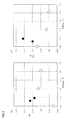
- FIG. 3 is a graph showing measurement results of solar cell characteristics when the surface area ratio Y is changed.
- FIG. 3A shows measurement results of the fill factor (FF) when the surface area ratio Y is changed.
- FIG. 3B shows the measurement result of the photoelectric conversion efficiency (Eff) when the surface area ratio Y is changed.
- the results of the examples are indicated by black circles, and the results of the comparative examples are indicated by diamonds.
- the results of Examples 1 and 2 and Comparative Examples 2 to 3 are shown with the FF value and Eff value of Comparative Example 1 being 1.000, respectively.
- Comparative Example 2 since the texture structure and the uneven shape are not formed on the back surface of the p-type silicon substrate, the passivation property of the back surface of the p-type silicon substrate is considered to be the best in Comparative Example 2. Therefore, in the following, the optimum range of the size of the back side uneven shape (specifically, the surface area ratio Y) was examined based on the Eff value of Comparative Example 2.
- the FF value tended to decrease when the surface area ratio Y was smaller than 1.05. The following can be considered as this reason.
- the surface area ratio Y is 1.00, that is, when the texture structure and the concavo-convex shape are not formed on the back surface of the p-type silicon substrate, the p-type silicon is formed at the time of forming the back-side electrode by vapor deposition. The adhesion of a metal such as aluminum to the back surface of the substrate is reduced. As a result, the FF value decreases.
- the Eff value increased as the surface area ratio Y decreased in the region where the surface area ratio Y was greater than 1.09, but decreased when the surface area ratio Y was less than 1.09. From this, it can be seen that the Eff value has a peak value rather than a maximum value when the surface area ratio Y is 1.00 (Comparative Example 2). 3 that the Eff value is larger than Comparative Example 2 and about 1% higher than Comparative Example 1 if the surface area ratio Y is 1.05 or more and 1.15 or less. On the other hand, when the surface area ratio Y was 1.20, the Eff value was lower than that of Comparative Example 2.
- the concave and convex shapes are formed on the light receiving surface of the p-type silicon substrate and the back surface of the p-type silicon substrate, and the back surface-side uneven shape 10 is made smaller than the light-receiving surface-side uneven shape 6, thereby
- the surface area ratio Y was set to 1.05 or more and 1.15 or less, the solar cell characteristics of the solar cell such as the fill factor and the photoelectric conversion efficiency were improved.
- 1 solar cell 2 p-type silicon substrate, 3 n-type semiconductor layer, 4 light receiving surface side electrode, 5 back surface side electrode, 6 light receiving surface side uneven shape, 7 antireflection film, 8 back surface electric field layer, 9 passivation film, 10 Uneven shape on the back side.
Landscapes
- Photovoltaic Devices (AREA)
Abstract
本発明の太陽電池(1)は、前記シリコン基板(2)の裏面に形成された裏面側凹凸形状(10)と裏面側電極(5)を備え、シリコン基板(2)の裏面の平面積をSとし、シリコン基板(2)の裏面側凹凸形状(10)の表面積をXとして、表面積比YをY=X/Sとしたとき、当該表面積比Yは1.05以上1.15以下であることを特徴とすることにより、裏面側電極(5)の密着強度の低下を招くことなく、かつシリコン基板(2)の裏面に存在するダングリングボンド増加を防止できる。
Description
本発明は、太陽電池および太陽電池の製造方法に関し、特に、光が入射される側とは反対側に位置する太陽電池の面(太陽電池の裏面)の構造に関する。
太陽光エネルギを直接電気エネルギに変換する太陽電池には、近年、特に地球環境問題の観点から、次世代のエネルギ源としての期待が急速に高まっている。太陽電池としては、化合物半導体材料を用いたもの、または、有機材料材料を用いたものなど様々な種類があるが、現在、主流となっている太陽電池は、シリコン結晶を用いたものである。
図4は、特許文献1(特開平9-237910号公報)に開示されている太陽電池21の構成の一例を模式的に示す断面図である。
図4に示す太陽電池21では、p型シリコン半導体基板11のうち光入射される側に位置する面(以下「p型シリコン半導体基板11の受光面」という。)にはn型シリコン半導体層12が形成され、n型シリコン半導体層12はシリコン酸化膜層13によって覆われており、シリコン酸化膜層13は反射防止膜層14によって覆われている。グリッド電極15は、反射防止膜層14とシリコン酸化膜層13とを貫通してn型シリコン半導体層12に接続されている。
p型シリコン半導体基板11の受光面とは反対側の面(以下「p型シリコン半導体基板11の裏面」という。)はシリコン酸化膜層16によって覆われており、シリコン酸化膜層16は水素化窒化シリコン膜層17によって覆われている。高濃度のp型半導体層であるp+型微結晶シリコン半導体層18は、水素化窒化シリコン膜層17を覆い、且つ、水素化窒化シリコン膜層17とシリコン酸化膜層16とを複数の部分において貫通してp型シリコン半導体基板11の裏面に接続されている。p+型微結晶シリコン半導体層18は、裏面電極19によって覆われている。
図5は、特許文献1に開示されている太陽電池の製造方法の一例を示すフロー図である。特許文献1には、以下に示す太陽電池の製造方法が一例として記載されている。
まず、p型シリコン半導体基板洗浄工程(S101。「S」はステップを表す。以下同様。)において、p型シリコン半導体基板11を洗浄する。次に、異方性エッチング工程(S102)において、p型シリコン半導体基板11の表面が凹凸になるように異方性エッチングを行なう。次に、pn接合形成工程(S103)において、POCl3を用いた気相拡散によってリンを拡散してn型シリコン半導体層12を形成する。
次に、裏面エッチング工程(S104)において、p型シリコン半導体基板11の裏面側をエッチングして、裏面に形成されたn型シリコン半導体層を除去する。次に、シリコン酸化膜層形成工程(S105)において、シリコン酸化膜層13およびシリコン酸化膜層16を熱酸化法で形成する。
次に、反射防止膜層形成工程(S106)において、窒化シリコン膜からなる反射防止膜層14をプラズマCVD法により形成する。次に、裏面水素化窒化シリコン膜層形成工程(S107)において、シリコン酸化膜層16上に水素化窒化シリコン膜層17を形成する。
次に、p+型の微結晶シリコン半導体層形成工程(S108)において、フォトエッチング法を用いて、水素化窒化シリコン膜層17およびシリコン酸化膜層16を加工する。その後、プラズマCVD法により、水素化窒化シリコン膜層17およびシリコン酸化膜層16を覆うようにp+型微結晶シリコン半導体層18を形成する。
次に、表裏電極形成工程(S109)において、蒸着法により、p+型微結晶シリコン半導体層18を覆うように裏面電極19を形成する。フォトエッチング法を用いてシリコン酸化膜層13および反射防止膜層14を加工した後、蒸着法によりグリッド電極15を形成する。このようにして、太陽電池21が製造される。
p型シリコン半導体基板の受光面にテクスチャ構造(テクスチャ構造とは、異方性エッチングにより形成された凹凸である)を形成する場合、製造ラインでは、一般的に、ウエットエッチングによる方法が多く用いられている。しかし、ウエットエッチングによりテクスチャ構造を形成すると、p型シリコン半導体基板の全面に(受光面だけでなく裏面および端面などにも)凹凸が形成されることになる。
しかしながら、p型シリコン半導体基板の裏面にテクスチャ構造が形成された状態では、p型シリコン半導体基板の裏面に凹凸形状が形成されていない状態に比べて、p型シリコン半導体基板の裏面の表面積が大きくなる。よって、p型シリコン半導体基板の裏面に存在するダングリングボンド数が多くなるので、キャリアの再結合が増加する。その結果、太陽電池特性に悪影響を及ぼしてしまうことになる。このことは、シリコン半導体基板としてn型シリコン半導体基板を用いた場合にも言える。
一方、p型シリコン半導体基板の裏面に凹凸形状が全く形成されていない状態では、p型シリコン半導体基板の裏面に存在するダングリングボンド数が減少するので、パッシベーション性は良好となる。しかし、p型シリコン半導体基板の裏面と裏面側電極との密着性に問題が生じ、太陽電池特性に悪影響が及ぼされることになる。このことも、シリコン半導体基板としてn型シリコン半導体基板を用いた場合にも言える。
本発明は、上記の問題に鑑みてなされたものであり、その目的は、シリコン基板の受光面および裏面のそれぞれに凹凸形状を有する太陽電池において、裏面側の凹凸形状の大きさを適正化することにより太陽電池特性を向上させることにある。
本発明に係る太陽電池は、第1導電型のシリコン基板と、シリコン基板の受光面に形成された受光面側凹凸形状と、シリコン基板の受光面に形成された第2導電型の半導体層と、シリコン基板の裏面に形成された裏面側凹凸形状と、シリコン基板の受光面上の一部に形成された受光面側電極と、シリコン基板の裏面上の一部に形成された裏面側電極とを備える。シリコン基板の裏面の平面積をSとし、シリコン基板の裏面側凹凸形状の表面積をXとして、表面積比YをY=X/Sとしたとき、当該表面積比Yが1.05以上1.15以下である。
ここで、本発明の太陽電池では、シリコン基板の裏面側凹凸形状は、シリコン基板の受光面側凹凸形状よりも小さくてもよい。
また、本発明の太陽電池では、裏面側電極は、アルミニウムからなってもよい。
本発明に係る太陽電池の製造方法は、第1導電型のシリコン基板にテクスチャ構造を形成する工程と、シリコン基板に第2導電型のドーパントを熱拡散させることにより、シリコン基板の受光面に第2導電型の半導体層を形成する工程と、シリコン基板の裏面をエッチングすることにより、シリコン基板の裏面に裏面側凹凸形状を形成する工程とを備える。シリコン基板の裏面に裏面側凹凸形状を形成する工程では、裏面側凹凸形状をシリコン基板の受光面に形成された受光面側凹凸形状よりも小さくする。
本発明に係る太陽電池の製造方法は、第1導電型のシリコン基板にテクスチャ構造を形成する工程と、シリコン基板に第2導電型のドーパントを熱拡散させることにより、シリコン基板の受光面に第2導電型の半導体層を形成する工程と、シリコン基板の裏面をエッチングすることにより、シリコン基板の裏面に裏面側凹凸形状を形成する工程とを備える。シリコン基板の裏面に裏面側凹凸形状を形成する工程では、裏面側凹凸形状をシリコン基板の受光面に形成された受光面側凹凸形状よりも小さくする。
ここで、本発明の太陽電池の製造方法においてシリコン基板の裏面に裏面側凹凸形状を形成する工程では、フッ素と硝酸との混合割合が体積比でフッ素:硝酸=1:5以上であるエッチング液を用いてシリコン基板の裏面をエッチングしてもよい。
本発明によれば、シリコン基板の裏面側凹凸形状の大きさが適正化されているので、太陽電池特性が向上する。
図1は、本発明の太陽電池の構成の一例を模式的に示す断面図である。以下では、特許請求の範囲における「第1導電型」および「第2導電型」がそれぞれ「p型」および「n型」である場合を示す。しかし、本発明には、特許請求の範囲における「第1導電型」および「第2導電型」がそれぞれ「n型」および「p型」である場合も含まれる。
図1に示す太陽電池1では、p型シリコン基板2のうち光が入射される側に位置する面(以下「p型シリコン基板2の受光面」という。)には、リンなどのn型のドーパントを用いた熱拡散法などによりn型半導体層3が形成されている。n型半導体層3の厚さは0.3μm程度であることが好ましい。これにより、p型シリコン基板2とn型半導体層3との界面にはpn接合が形成されている。
p型シリコン基板2の受光面上には、櫛状の金属電極である受光面側電極4が設けられている。受光面側電極4はたとえば銀からなることが好ましい。p型シリコン基板2の受光面には、テクスチャ構造である受光面側凹凸形状6が形成されており、受光面側凹凸形状6の上には、反射防止膜7が形成されている。反射防止膜7はたとえば窒化シリコン膜であることが好ましい。受光面側電極4は、反射防止膜7をパターニングまたはファイヤースルーすることにより形成された貫通孔内に設けられており、これによって、n型半導体層3と接している。
p型シリコン基板2の受光面とは反対側の面(以下「p型シリコン基板2の裏面」という。)上には、裏面側電極5が形成されている。裏面側電極5はたとえばアルミニウムからなることが好ましい。裏面側電極5の厚さはたとえば0.4μm以上8μm以下であることが好ましい。p型シリコン基板2の裏面には、パターニングされた裏面側電界層8(BSF(Back Surface Field)層)が形成され、p型シリコン基板2の裏面上には、パッシベーション膜9が形成されている。裏面側電界層8は、たとえばアルミニウムなどが拡散されて形成された拡散層であることが好ましく、裏面側電界層8の厚さは、たとえば1μm以上であることが好ましい。パッシベーション膜9はたとえば窒化シリコン膜であることが好ましく、パッシベーション膜9の厚さはたとえば0.06μm以上0.75μm以下であることが好ましい。このようなp型シリコン基板2の裏面には、裏面側凹凸形状10が形成されている。なお、図1では、受光面側凹凸形状6および裏面側凹凸形状10を模式的に記載しているにすぎず、受光面側凹凸形状6および裏面側凹凸形状10は実際にはランダムな凹凸形状である。
図1に示す太陽電池では、p型シリコン基板2の裏面の平面積をSとし、p型シリコン基板2の裏面側凹凸形状10の表面積をXとして、表面積比YをY=X/Sとしたとき、当該表面積比Yが1.05以上1.15以下である。なお、p型シリコン基板の裏面に凹凸形状が形成されていないときには、表面積比Yは1.0となる。
ここで、p型シリコン基板2の裏面の平面積は、p型シリコン基板2の裏面に凹凸形状が形成されていない状態における当該裏面の表面積である。p型シリコン基板2の裏面側凹凸形状10の表面積は、p型シリコン基板2の裏面に凹凸形状が形成された状態における当該裏面の表面積であり、たとえば共焦点レーザー走査型顕微鏡または走査型電子顕微鏡などを用いて求められる。
表面積比Yが1.05未満であれば、p型シリコン基板の裏面に対する受光面側電極の密着強度の低下を招く。そのため、曲線因子などの低下を招く。一方、表面積比Yが1.15を超えると、p型シリコン基板の裏面に存在するダングリングボンド数の増加を招くため、キャリアの再結合が増加し、よって、光電変換効率などの低下を招く。しかし、表面積比Yが1.05以上1.15以下であれば、p型シリコン基板2の裏面に対する受光面側電極4の密着強度が確保され、また、p型シリコン基板2の裏面に存在するダングリングボンド数の増加を防止できる。よって、曲線因子および光電変換効率などの太陽電池特性が向上する。
図1に示す太陽電池では、裏面側凹凸形状10は、受光面側凹凸形状6よりも小さいことが好ましい。ここで、「凹凸形状が小さい」とは、高低差が小さいことを意味する。裏面側凹凸形状の大きさが受光面側凹凸形状の大きさ以上であれば、p型シリコン基板の裏面に存在するダングリングボンド数が過剰となることがある。しかし、裏面側凹凸形状10が受光面側凹凸形状6よりも小さければ、p型シリコン基板2の裏面に存在するダングリングボンド数が最適化されるため、光電変換効率などが向上する。
図1に示す太陽電池の製造方法を示す。図2は、図1に示す太陽電池の製造方法の一例を示すフロー図である。
まず、テクスチャリング工程(S1。「S」はステップを表す。以下同様。)では、p型シリコン基板2の全面、すなわちp型シリコン基板2の受光面となる面(以下では「p型シリコン基板2の受光面」という。)、p型シリコン基板2の裏面となる面(以下では「p型シリコン基板2の裏面」という。)およびp型シリコン基板2の端面に、ウエットエッチング法によりテクスチャ構造を形成する。ウエットエッチング法では、酸性溶液またはアルカリ性溶液を用いることができる。これにより、p型シリコン基板2の受光面に、受光面側凹凸形状6が形成される。
次に、pn接合の形成工程(S2)において、p型シリコン基板2の受光面にn型半導体層3を形成する。これにより、p型シリコン基板2とn型半導体層3との界面にpn接合が形成される。n型半導体層3の形成時にガラス層であるPSG(Phosphosilicate Glass)層がn型半導体層3上に形成された場合には、n型半導体層3の形成後に、たとえば希フッ酸などを用いて当該PSG層を除去することが好ましい。
n型半導体層3の形成方法としては、たとえば、n型のドーパントを含む気体を用いた熱拡散法を用いることができる。具体的には、拡散材料としてn型のドーパントを含むガスを用い、チューブ炉にて800℃以上の温度でp型シリコン基板2を熱処理する。これにより、n型のドーパントが気相拡散して、p型シリコン基板2の表面全体の上にn型半導体層3が形成される。n型のドーパントとしてリンを選択した場合には、n型のドーパントを含むガスとしてPOCl3などを用いることができる。なお、n型半導体層3がp型シリコン基板2の受光面だけでなくp型シリコン基板2の裏面および端面にも形成されることがあるが、p型シリコン基板2の裏面および端面に形成されたn型半導体層3は後述する裏面エッチング工程(S4)においてエッチング除去される。
n型半導体層3の形成方法としては、熱拡散法ではなく、n型のドーパントを含む溶液(たとえばPSG液)をp型シリコン基板2の受光面に塗布してから熱処理を行うという塗布拡散法を用いることもできる。
次に、反射防止膜の形成工程(S3)において、n型半導体層3上に反射防止膜7を形成する。反射防止膜7として窒化シリコン膜を用いる場合には、ガス種としてシランおよびアンモニアを用いたプラズマCVD法により厚さが70nm程度の反射防止膜7を形成することが好ましい。
次に、裏面エッチング工程(S4)において、p型シリコン基板2の裏面をエッチングする。これにより、p型シリコン基板2の裏面には、裏面側凹凸形状10が形成される。
具体的には、まず、p型シリコン基板2の受光面に、エッチングを防止するための保護テープを貼る。この保護テープの材料は、特に限定されないが、次工程におけるエッチングにおいて使用されるエッチング液に対する耐性を有することが好ましい。次工程ではエッチング液として酸性溶液を用いるため、保護テープは耐酸性を有することが好ましい。次に、p型シリコン基板2の裏面をウエットエッチングする。これにより、p型シリコン基板2の裏面上に形成されていたn型半導体層3が除去されるとともに、p型シリコン基板2の裏面には裏面側凹凸形状10が形成される。また、p型シリコン基板2の端面上に形成されていたn型半導体層3も除去される。
裏面側凹凸形状10は、本工程により、上記テクスチャリング工程(S1)においてp型シリコン基板2の裏面に形成されたテクスチャ構造をなだらかにする(テクスチャ構造の高低差を小さくする)ことにより形成される。よって、本工程を行なえば、p型シリコン基板2の裏面の表面積が小さくなるので、p型シリコン基板2の裏面に存在するダングリングボンド数が減少する。したがって、裏面側凹凸形状10が形成されると、p型シリコン基板の裏面にテクスチャ構造が残存している場合に比べ、p型シリコン基板2の裏面の表面積が小さくなるので、当該裏面に存在するダングリングボンド数が減少する。
このようにして裏面側凹凸形状10を形成するため、裏面側凹凸形状10は受光面側凹凸形状6よりも小さくなる。表面積比Yが1.05以上1.15以下となるように裏面側凹凸形状10を形成することが好ましい。これにより、曲線因子および光電変換効率などの太陽電池特性に優れた太陽電池を製造することができる。
本工程におけるウエットエッチングの条件は特に限定されない。たとえば、フッ酸(HF)と硝酸(HNO3)との混合溶液をエッチング液として使用することが好ましい。この混合溶液における混合割合は、体積比で、フッ酸(HF):硝酸(HNO3)=1:5以上1:50以下であることが好ましい。フッ酸と硝酸との混合割合が上記範囲外であれば、ウエットエッチングのエッチングレートが速くなりすぎることがある。その結果、上記テクスチャリング工程(S1)においてp型シリコン基板2の裏面に形成されたテクスチャ構造が完全に除去されることがあるため、裏面側凹凸形状10を形成できない場合がある。また、硝酸との混合割合が上記範囲以上であれば、ウエットエッチングのエッチングレートが遅くなりすぎることもある。その結果、裏面側凹凸形状10を形成することはできるが、スループットの低下を招く。しかし、この混合溶液における混合割合が体積比でフッ酸(HF):硝酸(HNO3)=1:5以上1:50以下であれば、ウエットエッチングのエッチングレートが最適化される。よって、表面積比Yが1.05以上1.15以下である裏面側凹凸形状10が形成され、裏面側凹凸形状10は受光面側凹凸形状6よりも小さくなる。それだけでなく、スループットの低下を防止することもできる。以上より、曲線因子および光電変換効率などの太陽電池特性に優れた太陽電池を生産性良く製造することができる。
p型シリコン基板2をエッチング液に浸漬させる時間は、5秒以上であることが好ましい。これにより、表面積比Yが1.05以上1.15以下である裏面側凹凸形状10が形成されるので、曲線因子および光電変換効率などの太陽電池特性により優れた太陽電池を製造することができる。浸漬時間が5秒未満であれば、上記テクスチャリング工程(S1)においてp型シリコン基板2の裏面に形成されたテクスチャ構造をなだらかにする(テクスチャ構造の高低差を小さくする)ことができない場合がある。そのため、p型シリコン基板2の裏面に存在するダングリングボンド数の増加を招くことがある。一方、浸漬時間が長くなりすぎると、上記テクスチャリング工程(S1)においてp型シリコン基板2の裏面に形成されたテクスチャ構造が完全に除去されるおそれがあり、裏面側凹凸形状が形成されないことがある。
エッチング液は10℃以上40℃以下であることが好ましい。これにより、エッチングレートが最適化されるので、太陽電池特性だけでなく太陽電池の生産性の向上も図ることができる。
次に、パッシベーション膜の形成工程(S5)において、たとえば希フッ酸などを用いてp型シリコン基板2の裏面上に残ったシリコン酸化膜を除去した後、たとえばプラズマCVD法などによってパッシベーション膜9を裏面側凹凸形状10上に形成する。パッシベーション膜9としては窒化シリコン膜を形成することが好ましい。
次に、パッシベーション膜のパターニング工程(S6)において、たとえばフォトリソグラフィ法などによりパッシベーション膜9を所定の形状を有する裏面側電界層パターンにエッチングし、パッシベーション膜9を貫通するコンタクト孔を形成する。
次に、裏面側電界層の形成工程(S7)において、たとえばスクリーン印刷法などによって、パターニングされたパッシベーション膜9上に、アルミニウム粉末、ガラスフリット、樹脂および有機溶媒などからなるアルミニウムペーストを印刷する。アルミニウムペーストが乾燥したら、p型シリコン基板2を700℃以上にて焼成する。これにより、コンタクト孔に対応した箇所のp型シリコン基板2の裏面側にアルミニウムが拡散し、アルミニウムの拡散層からなる裏面側電界層8が形成される。その後、p型シリコン基板2の裏面上に残ったアルミニウムなどをたとえば塩酸などにて除去する。
次に、裏面側電極の形成工程(S8)において、たとえば真空蒸着法などにより、パターニングされたパッシベーション膜9上にアルミニウムなどの金属を蒸着する。これにより、裏面側電極5が形成される。このとき、コンタクト孔内にも、アルミニウムなどの金属が蒸着されて充填される。
次に、受光面側電極の形成工程(S9)において、たとえばスクリーン印刷法などにより、反射防止膜7上に、銀粉末、ガラスフリット、樹脂および有機溶媒などからなる銀ペーストを印刷する。銀ペーストが乾燥したら、p型シリコン基板2を500℃以上にて焼成する。これにより、銀からなる受光面側電極4が形成される。なお、受光面側電極4は、銀ペーストがp型シリコン基板2の焼成時に反射防止膜7を突き破ることにより形成され、すなわち銀ペーストが反射防止膜7をファイヤースルーすることにより形成される。これにより、受光面側電極4は、n型半導体層3と電気的に接続される。このようにして、図1に示す太陽電池1が製造される。
なお、太陽電池1の構成要素の材料は上記記載に限定されない。また、太陽電池1の構成要素の厚さなども上記記載に限定されない。
100mm角、厚さ100~200μmのp型シリコン基板を用いて、図2に示す太陽電池1の製造方法にしたがって、太陽電池を製造した。この際、裏面エッチング工程(S4)においてエッチング時間(n型シリコン基板をエッチング液に浸漬させる時間)を変化させることにより裏面側凹凸形状の大きさを変え、製造された太陽電池の太陽電池特性を調べた。
裏面エッチング工程(S4)の後でp型シリコン基板の裏面の表面積比Yを求めることにより、裏面側凹凸形状10の大きさを評価した。表面積比Yは、下記式(1)を用いて求めた。ここで、下記式(1)における「S」はp型シリコン基板の裏面の平面積であり、「X」はp型シリコン基板の裏面側凹凸形状の表面積である
表面積比YをY=X/S・・・式(1)。
表面積比YをY=X/S・・・式(1)。
なお、p型シリコン基板の裏面側凹凸形状の表面積は、レーザ顕微鏡(波長:408nm)を用いて、測定器として共焦点レーザー走査型顕微鏡(OLYMPUS社製の「LEXT OLS3000」を用いて、求められた。
表面積比Yは、比較例1では1.41であり、比較例2では1.00であった。また、実施例1~2および比較例1~3では、フッ素と硝酸との混合割合が体積比でフッ素:硝酸=1:5であるエッチング液を用いて、裏面エッチング(S4)を行なった。
比較例1の裏面エッチング工程(S4)では、pn接合の形成工程(S2)においてp型シリコン基板の裏面上に形成されたn型半導体層のみが除去されたに過ぎず、テクスチャリング工程(S1)においてp型シリコン基板の裏面上に形成されたテクスチャ構造は除去されずに残存した。一方、比較例2の裏面エッチング工程(S4)では、p型シリコン基板の裏面上に形成されたテクスチャ構造も除去された。
図3は、表面積比Yを変化させた場合の太陽電池特性の測定結果を示すグラフであり、図3(a)には、表面積比Yを変化させた場合の曲線因子(FF)の測定結果を示し、図3(b)には、表面積比Yを変化させた場合の光電変換効率(Eff)の測定結果を示す。なお、図3(a)~(b)では、実施例の結果を黒丸で示し、比較例の結果を菱形で示している。比較例1のFF値およびEff値をそれぞれ1.000として、実施例1~2および比較例2~3の結果を示している。比較例2ではp型シリコン基板の裏面にテクスチャ構造および凹凸形状などが形成されていないので、p型シリコン基板の裏面のパッシベーション性は比較例2で最も良好になると考えられる。よって、以下では、比較例2のEff値を基準として裏面側凹凸形状の大きさ(具体的には表面積比Y)の最適な範囲を検討した。
図3(a)から、FF値は、表面積比Yが1.05より小さくなると減少する傾向となった。この理由としては、次に示すことが考えられる。表面積比Yが1.00である場合には、すなわちp型シリコン基板の裏面にテクスチャ構造および凹凸形状などが形成されていない場合には、蒸着法による裏面側電極の形成時において、p型シリコン基板の裏面に対するアルミニウムなどの金属の密着性が低下する。その結果、FF値が減少する。
また、図3(b)から、Eff値は、表面積比Yが1.09より大きい領域では表面積比Yの減少に伴って増加したが、表面積比Yが1.09を下回ると減少した。このことから、Eff値は、表面積比Yが1.00(比較例2)で最大値をとるのではなく、ピーク値を持つことがわかる。そして、図3より、表面積比Yが1.05以上1.15以下であれば、Eff値は、比較例2よりも大きくなり、比較例1よりも1%程度向上することがわかる。一方、表面積比Yが1.20では、Eff値は比較例2よりも低かった。
以上より、p型シリコン基板の受光面およびp型シリコン基板の裏面のそれぞれに凹凸形状を形成し、裏面側凹凸形状10を受光面側凹凸形状6よりも小さくすることによりp型シリコン基板の裏面の表面積比Yを1.05以上1.15以下にすれば、曲線因子および光電変換効率などの太陽電池の太陽電池特性が向上した。
なお、本実施例では、p型シリコン基板について検討したが、n型シリコン基板でも同様の結果が得られた。
今回開示された実施の形態および実施例はすべての点で例示であって制限的なものではないと考えられるべきである。本発明の範囲は上記した説明ではなくて請求の範囲によって示され、請求の範囲と均等の意味および範囲内でのすべての変更が含まれることが意図される。
1 太陽電池、2 p型シリコン基板、3 n型半導体層、4 受光面側電極、5 裏面側電極、6 受光面側凹凸形状、7 反射防止膜、8 裏面側電界層、9 パッシベーション膜、10 裏面側凹凸形状。
Claims (5)
- 第1導電型のシリコン基板(2)と、
前記シリコン基板(2)の受光面に形成された受光面側凹凸形状(6)と、
前記シリコン基板(2)の受光面に形成された第2導電型の半導体層(3)と、
前記シリコン基板(2)の裏面に形成された裏面側凹凸形状(10)と、
前記シリコン基板(2)の受光面上の一部に形成された受光面側電極(4)と、
前記シリコン基板(2)の裏面上の一部に形成された裏面側電極(5)とを備え、
前記シリコン基板(2)の裏面の平面積をSとし、前記シリコン基板(2)の裏面側凹凸形状(10)の表面積をXとして、表面積比YをY=X/Sとしたとき、当該表面積比Yが1.05以上1.15以下である太陽電池(1)。 - 前記シリコン基板(2)の前記裏面側凹凸形状(10)は、前記シリコン基板(2)の前記受光面側凹凸形状(6)よりも小さい請求項1に記載の太陽電池(1)。
- 前記裏面側電極(5)は、アルミニウムからなる請求項1または2に記載の太陽電池(1)。
- 第1導電型のシリコン基板(2)にテクスチャ構造を形成する工程と、
前記シリコン基板(2)に第2導電型のドーパントを熱拡散させることにより、前記シリコン基板(2)の受光面に第2導電型の半導体層(3)を形成する工程と、
前記シリコン基板(2)の裏面をエッチングすることにより、前記シリコン基板(2)の裏面に裏面側凹凸形状(10)を形成する工程とを備え、
前記シリコン基板(2)の裏面に前記裏面側凹凸形状(10)を形成する工程では、前記裏面側凹凸形状(10)を前記シリコン基板(2)の受光面に形成された受光面側凹凸形状(6)よりも小さくする太陽電池(1)の製造方法。 - 前記シリコン基板(2)の裏面に前記裏面側凹凸形状(10)を形成する工程では、フッ素と硝酸との混合割合が体積比でフッ素:硝酸=1:5以上1:50以下であるエッチング液を用いて前記シリコン基板(2)の裏面をエッチングする請求項4に記載の太陽電池(1)の製造方法。
Applications Claiming Priority (2)
| Application Number | Priority Date | Filing Date | Title |
|---|---|---|---|
| JP2011-138048 | 2011-06-22 | ||
| JP2011138048A JP5715509B2 (ja) | 2011-06-22 | 2011-06-22 | 太陽電池、及び太陽電池の製造方法 |
Publications (1)
| Publication Number | Publication Date |
|---|---|
| WO2012176838A1 true WO2012176838A1 (ja) | 2012-12-27 |
Family
ID=47422669
Family Applications (1)
| Application Number | Title | Priority Date | Filing Date |
|---|---|---|---|
| PCT/JP2012/065863 Ceased WO2012176838A1 (ja) | 2011-06-22 | 2012-06-21 | 太陽電池および太陽電池の製造方法 |
Country Status (2)
| Country | Link |
|---|---|
| JP (1) | JP5715509B2 (ja) |
| WO (1) | WO2012176838A1 (ja) |
Families Citing this family (1)
| Publication number | Priority date | Publication date | Assignee | Title |
|---|---|---|---|---|
| JP5991945B2 (ja) * | 2013-06-07 | 2016-09-14 | 信越化学工業株式会社 | 太陽電池および太陽電池モジュール |
Citations (4)
| Publication number | Priority date | Publication date | Assignee | Title |
|---|---|---|---|---|
| JP2004235274A (ja) * | 2003-01-28 | 2004-08-19 | Kyocera Corp | 多結晶シリコン基板およびその粗面化法 |
| WO2005117138A1 (ja) * | 2004-05-28 | 2005-12-08 | Sharp Kabushiki Kaisha | 太陽電池用半導体基板とその製造方法および太陽電池 |
| JP2010278401A (ja) * | 2009-06-01 | 2010-12-09 | Sharp Corp | シリコンシート、太陽電池およびその製造方法 |
| JP2011009247A (ja) * | 2009-06-23 | 2011-01-13 | Sharp Corp | 太陽電池の製造方法及び湿式エッチング装置 |
-
2011
- 2011-06-22 JP JP2011138048A patent/JP5715509B2/ja not_active Ceased
-
2012
- 2012-06-21 WO PCT/JP2012/065863 patent/WO2012176838A1/ja not_active Ceased
Patent Citations (4)
| Publication number | Priority date | Publication date | Assignee | Title |
|---|---|---|---|---|
| JP2004235274A (ja) * | 2003-01-28 | 2004-08-19 | Kyocera Corp | 多結晶シリコン基板およびその粗面化法 |
| WO2005117138A1 (ja) * | 2004-05-28 | 2005-12-08 | Sharp Kabushiki Kaisha | 太陽電池用半導体基板とその製造方法および太陽電池 |
| JP2010278401A (ja) * | 2009-06-01 | 2010-12-09 | Sharp Corp | シリコンシート、太陽電池およびその製造方法 |
| JP2011009247A (ja) * | 2009-06-23 | 2011-01-13 | Sharp Corp | 太陽電池の製造方法及び湿式エッチング装置 |
Also Published As
| Publication number | Publication date |
|---|---|
| JP2013004944A (ja) | 2013-01-07 |
| JP5715509B2 (ja) | 2015-05-07 |
Similar Documents
| Publication | Publication Date | Title |
|---|---|---|
| US20220123158A1 (en) | Efficient black silicon photovoltaic devices with enhanced blue response | |
| JP4481869B2 (ja) | 太陽電池の製造方法及び太陽電池並びに半導体装置の製造方法 | |
| JP5215330B2 (ja) | 裏面電極型太陽電池の製造方法、裏面電極型太陽電池および裏面電極型太陽電池モジュール | |
| JP5414298B2 (ja) | 太陽電池の製造方法 | |
| JP6482692B2 (ja) | 太陽電池素子 | |
| AU2006243111A1 (en) | Solar cell manufacturing method and solar cell | |
| JP2004006565A (ja) | 太陽電池とその製造方法 | |
| RU2626053C2 (ru) | Солнечная батарея и способ ее изготовления | |
| KR20130023219A (ko) | 태양 전지 | |
| JP5991945B2 (ja) | 太陽電池および太陽電池モジュール | |
| JP5004932B2 (ja) | 太陽電池および太陽電池の製造方法 | |
| JPWO2013100085A1 (ja) | 太陽電池素子、太陽電池素子の製造方法および太陽電池モジュール | |
| CN103137786A (zh) | 光伏装置及其制造方法 | |
| JP2013030665A (ja) | 光電変換装置モジュール、光電変換装置モジュールの製造方法、及び光電変換装置 | |
| CN103222064A (zh) | 背面电极型太阳能电池 | |
| JP6114171B2 (ja) | 太陽電池の製造方法 | |
| JP5715509B2 (ja) | 太陽電池、及び太陽電池の製造方法 | |
| JP6392717B2 (ja) | 太陽電池セルの製造方法 | |
| JP5994895B2 (ja) | 太陽電池の製造方法 | |
| JP2011243726A (ja) | 太陽電池の製造方法 | |
| JP2011243758A (ja) | 太陽電池の製造方法 | |
| KR20130113002A (ko) | 식각 용액 보호층을 이용한 선택적 에미터층을 형성하는 방법 | |
| KR20150081816A (ko) | 높은 반송자 수명을 가지는 에미터층을 갖는 고효율 태양전지 기판의 제조방법 및 이를 포함하는 태양전지 |
Legal Events
| Date | Code | Title | Description |
|---|---|---|---|
| 121 | Ep: the epo has been informed by wipo that ep was designated in this application |
Ref document number: 12802635 Country of ref document: EP Kind code of ref document: A1 |
|
| NENP | Non-entry into the national phase |
Ref country code: DE |
|
| 122 | Ep: pct application non-entry in european phase |
Ref document number: 12802635 Country of ref document: EP Kind code of ref document: A1 |