WO2012176411A1 - トランジスタ用半導体基板、トランジスタ及びトランジスタ用半導体基板の製造方法 - Google Patents
トランジスタ用半導体基板、トランジスタ及びトランジスタ用半導体基板の製造方法 Download PDFInfo
- Publication number
- WO2012176411A1 WO2012176411A1 PCT/JP2012/003908 JP2012003908W WO2012176411A1 WO 2012176411 A1 WO2012176411 A1 WO 2012176411A1 JP 2012003908 W JP2012003908 W JP 2012003908W WO 2012176411 A1 WO2012176411 A1 WO 2012176411A1
- Authority
- WO
- WIPO (PCT)
- Prior art keywords
- crystal layer
- semiconductor substrate
- epitaxial crystal
- layer
- epitaxial
- Prior art date
- Legal status (The legal status is an assumption and is not a legal conclusion. Google has not performed a legal analysis and makes no representation as to the accuracy of the status listed.)
- Ceased
Links
Images


Classifications
-
- H—ELECTRICITY
- H10—SEMICONDUCTOR DEVICES; ELECTRIC SOLID-STATE DEVICES NOT OTHERWISE PROVIDED FOR
- H10D—INORGANIC ELECTRIC SEMICONDUCTOR DEVICES
- H10D62/00—Semiconductor bodies, or regions thereof, of devices having potential barriers
- H10D62/80—Semiconductor bodies, or regions thereof, of devices having potential barriers characterised by the materials
- H10D62/85—Semiconductor bodies, or regions thereof, of devices having potential barriers characterised by the materials being Group III-V materials, e.g. GaAs
- H10D62/8503—Nitride Group III-V materials, e.g. AlN or GaN
-
- H—ELECTRICITY
- H10—SEMICONDUCTOR DEVICES; ELECTRIC SOLID-STATE DEVICES NOT OTHERWISE PROVIDED FOR
- H10D—INORGANIC ELECTRIC SEMICONDUCTOR DEVICES
- H10D62/00—Semiconductor bodies, or regions thereof, of devices having potential barriers
- H10D62/80—Semiconductor bodies, or regions thereof, of devices having potential barriers characterised by the materials
- H10D62/85—Semiconductor bodies, or regions thereof, of devices having potential barriers characterised by the materials being Group III-V materials, e.g. GaAs
- H10D62/852—Semiconductor bodies, or regions thereof, of devices having potential barriers characterised by the materials being Group III-V materials, e.g. GaAs being Group III-V materials comprising three or more elements, e.g. AlGaN or InAsSbP
-
- H—ELECTRICITY
- H10—SEMICONDUCTOR DEVICES; ELECTRIC SOLID-STATE DEVICES NOT OTHERWISE PROVIDED FOR
- H10P—GENERIC PROCESSES OR APPARATUS FOR THE MANUFACTURE OR TREATMENT OF DEVICES COVERED BY CLASS H10
- H10P14/00—Formation of materials, e.g. in the shape of layers or pillars
- H10P14/20—Formation of materials, e.g. in the shape of layers or pillars of semiconductor materials
- H10P14/29—Formation of materials, e.g. in the shape of layers or pillars of semiconductor materials characterised by the substrates
- H10P14/2901—Materials
-
- H—ELECTRICITY
- H10—SEMICONDUCTOR DEVICES; ELECTRIC SOLID-STATE DEVICES NOT OTHERWISE PROVIDED FOR
- H10P—GENERIC PROCESSES OR APPARATUS FOR THE MANUFACTURE OR TREATMENT OF DEVICES COVERED BY CLASS H10
- H10P14/00—Formation of materials, e.g. in the shape of layers or pillars
- H10P14/20—Formation of materials, e.g. in the shape of layers or pillars of semiconductor materials
- H10P14/34—Deposited materials, e.g. layers
- H10P14/3402—Deposited materials, e.g. layers characterised by the chemical composition
-
- H—ELECTRICITY
- H10—SEMICONDUCTOR DEVICES; ELECTRIC SOLID-STATE DEVICES NOT OTHERWISE PROVIDED FOR
- H10P—GENERIC PROCESSES OR APPARATUS FOR THE MANUFACTURE OR TREATMENT OF DEVICES COVERED BY CLASS H10
- H10P14/00—Formation of materials, e.g. in the shape of layers or pillars
- H10P14/20—Formation of materials, e.g. in the shape of layers or pillars of semiconductor materials
- H10P14/34—Deposited materials, e.g. layers
- H10P14/3402—Deposited materials, e.g. layers characterised by the chemical composition
- H10P14/3414—Deposited materials, e.g. layers characterised by the chemical composition being group IIIA-VIA materials
- H10P14/3416—Nitrides
-
- H—ELECTRICITY
- H10—SEMICONDUCTOR DEVICES; ELECTRIC SOLID-STATE DEVICES NOT OTHERWISE PROVIDED FOR
- H10P—GENERIC PROCESSES OR APPARATUS FOR THE MANUFACTURE OR TREATMENT OF DEVICES COVERED BY CLASS H10
- H10P14/00—Formation of materials, e.g. in the shape of layers or pillars
- H10P14/20—Formation of materials, e.g. in the shape of layers or pillars of semiconductor materials
- H10P14/34—Deposited materials, e.g. layers
- H10P14/3438—Doping during depositing
- H10P14/3441—Conductivity type
- H10P14/3446—Transition metal elements; Rare earth elements
-
- H—ELECTRICITY
- H10—SEMICONDUCTOR DEVICES; ELECTRIC SOLID-STATE DEVICES NOT OTHERWISE PROVIDED FOR
- H10D—INORGANIC ELECTRIC SEMICONDUCTOR DEVICES
- H10D30/00—Field-effect transistors [FET]
- H10D30/40—FETs having zero-dimensional [0D], one-dimensional [1D] or two-dimensional [2D] charge carrier gas channels
- H10D30/47—FETs having zero-dimensional [0D], one-dimensional [1D] or two-dimensional [2D] charge carrier gas channels having two-dimensional [2D] charge carrier gas channels, e.g. nanoribbon FETs or high electron mobility transistors [HEMT]
- H10D30/471—High electron mobility transistors [HEMT] or high hole mobility transistors [HHMT]
- H10D30/475—High electron mobility transistors [HEMT] or high hole mobility transistors [HHMT] having wider bandgap layer formed on top of lower bandgap active layer, e.g. undoped barrier HEMTs such as i-AlGaN/GaN HEMTs
Definitions
- the present invention relates to a semiconductor substrate for a transistor, a transistor, and a method for manufacturing the semiconductor substrate for a transistor.
- HEMT High Electron Mobility Transistor
- a Schottky layer is made of AlGaN and a channel layer is made of InGaN or GaN (this form is referred to as AlGaN / GaN below).
- HEMT High Electron Mobility Transistor
- AlGaN / GaN HEMT has a large leakage current from the gate.
- the electric field applied to the heterointerface between the AlGaN layer and the (In) GaN layer is in the forward direction, so that the leakage current increases accordingly.
- Non-Patent Document 1 H. Sazawa et al., Physica status solidi (c), 4, (2007) 2748
- piezoelectric polarization occurs in the AlGaN layer due to the difference in lattice constant between the AlGaN Schottky layer and the GaN layer or InGaN layer.
- piezo polarization occurs, a two-dimensional electron gas is generated on the GaN layer side or the InGaN layer side of the heterointerface in order to cancel the piezo polarization.
- Piezo polarization increases as the thickness of the AlGaN layer and the Al composition ratio increase, and the concentration of the two-dimensional electron gas increases accordingly.
- the HEMT threshold shifts to the minus side. That is, in the HEMT having the AlGaN / GaN heterostructure, it is difficult to achieve both the suppression of the leakage current and the realization of a high threshold value. For this reason, it has been difficult to produce a HEMT that has a small leakage current and that operates normally off.
- MIS-HEMT In the MIS-HEMT in which an insulating layer is disposed between the AlGaN layer and the gate, it is possible to achieve both normally-off operation and suppression of leakage current. However, in order to manufacture MIS-HEMT, it is necessary to form an insulating layer, which increases the manufacturing cost. Further, since the MIS-HEMT has an insulating layer between the AlGaN layer and the gate, there is a problem that the variation in threshold value is larger than that of the Schottky HEMT. In addition, it is difficult to keep the interface state density generated at the interface between the insulating film and the AlGaN layer low, and the device characteristics tend to exhibit hysteresis.
- a base substrate a first epitaxial crystal layer made of a first crystal of a nitride containing a group IIIa element, provided on the base substrate, and provided on the first epitaxial crystal layer are provided.
- a second epitaxial crystal layer comprising a second crystal of a nitride having a larger band gap than the first crystal and including a group IIIa element and a group IIIb element in which a part of the group IIIa element is substituted.
- a semiconductor substrate for a transistor In the semiconductor substrate, the second epitaxial crystal layer may be lattice matched or pseudo lattice matched to the first epitaxial crystal layer.
- the first crystal is In x Al y Ga 1-xy N (where 0 ⁇ x ⁇ 1, 0 ⁇ y ⁇ 1)
- the second crystal is M q Al z.
- Ga 1-q-z N M is one or more elements selected from the group of scandium, yttrium and lanthanoid elements, and 0 ⁇ q ⁇ 0.30, 0 ⁇ z ⁇ 1, q + z ⁇ 1 is there.
- the second crystal is, for example, Y q Al z Ga 1- qz N (0 ⁇ q ⁇ 0.30, 0 ⁇ z ⁇ 1, q + z ⁇ 1).
- the conductivity type of the second epitaxial crystal layer is, for example, n-type or insulating type.
- An example of the first crystal is GaN.
- M in M q Al z Ga 1-qz N is yttrium or scandium, and the q / z value is 0.1 to 0.35. A range is preferable.
- the crystal type of the first crystal or the second crystal is preferably a wurtzite type.
- a two-dimensional carrier gas is provided that includes the semiconductor substrate of the first aspect and is generated closer to the first epitaxial crystal layer than the interface between the first epitaxial crystal layer and the second epitaxial crystal layer.
- a transistor having a channel as a channel is provided.
- the carrier is an electron
- the upper surface side of the crystal may be group III polarity
- the carrier is a hole
- it may be group V polarity.
- the transistor can perform a normally-off operation.
- a second epitaxial crystal layer is formed by epitaxially growing a second crystal of a nitride having a band gap larger than one crystal and including a group IIIa element and a group IIIb element in which a part of the group IIIa element is substituted.
- IIIa group refers to the boron group
- IIIb group refers to the scandium group
- Group IIIa and group IIIb are names in the old CAS system.
- FIG. 1 shows a cross section of a semiconductor substrate 100 according to an embodiment of the present invention.
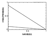
- An example of the relationship between the composition ratio of GaN and the composition ratio of AlN and YN in Y q Al z Ga 1- qz N lattice-matched with GaN calculated according to Vegard's law is shown.
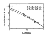
- the relationship between the composition ratio of GaN and the band gap of Y q Al z Ga 1-qz N having the ratio of q and z shown in FIG. 2 is shown. It shows an example of the relationship between Sc q Al z Ga 1-q -z GaN composition ratio in N and AlN and ScN composition ratio of GaN and lattice matching.
- FIG. 1 shows a cross section of a semiconductor substrate 100 according to an embodiment of the present invention.
- the semiconductor substrate 100 includes a base substrate 110, a first epitaxial crystal layer 120, and a second epitaxial crystal layer 130.
- the base substrate 110 is a substrate made of, for example, Al 2 O 3 , Si, SiC, ZnO, or GaN.
- the first epitaxial crystal layer 120 is composed of a first crystal of nitride containing a group IIIa element.
- the first crystal constituting the first epitaxial crystal layer 120 is, for example, In x Al y Ga 1-xy N (where 0 ⁇ x ⁇ 1, 0 ⁇ y ⁇ 1).
- the second epitaxial crystal layer 130 is provided on the first epitaxial crystal layer 120.
- the second epitaxial crystal layer 130 is composed of a second crystal having a larger band gap than the first crystal.
- the second crystal constituting the second epitaxial crystal layer 130 is, for example, a nitride containing a group IIIa element and a group IIIb element in which a part of the group IIIa element is substituted.
- at least one group IIIa element is not common between the group IIIa element contained in the first crystal and the group IIIa element contained in the second crystal.
- the first crystal and the second crystal may include a common group IIIa element.
- the first crystal contains In and Al as a group IIIa element
- the second crystal contains Al as a group IIIa element and does not contain In.
- the composition ratio of the common group IIIa elements may be different between the group IIIa element contained in the first crystal and the group IIIa element contained in the second crystal.
- Second crystals constituting the second epitaxial crystal layer 130 is, for example, M q Al z Ga 1-q -z N.
- M is one or more elements selected from scandium, yttrium, and lanthanoid elements, and 0 ⁇ q ⁇ 0.30, 0 ⁇ z ⁇ 1, and q + z ⁇ 1.
- the lattice constant difference between the first epitaxial crystal layer 120 and the second epitaxial crystal layer 130 can be reduced.
- the concentration of the two-dimensional carrier gas generated by piezo polarization decreases, and the threshold value of HEMT formed using the semiconductor substrate 100 shifts to the plus side when the carriers are electrons, and to the minus side when the carriers are holes. .
- the transistor can be normally off.
- the second epitaxial crystal layer 130 may be a nitride containing a group IIIa element and a group IIIb element in various ratios.
- the second epitaxial crystal layer 130 has a group IIIa element and a group IIIb element in a ratio of (0.70 to 0.95) :( 0.30 to 0.05).
- the composition ratio q / z between the group IIIb element represented by M and Al in the second epitaxial crystal layer 130 is in the range of 0.1 to 0.25. It's okay.
- the composition ratio q / z may be in the range of 0.1 to 0.35.
- the conductivity type of the second epitaxial crystal layer 130 may be n-type or semi-insulating.
- the second crystal constituting the second epitaxial crystal layer 130 has a larger band gap than the first crystal constituting the first epitaxial crystal layer 120. Therefore, the second epitaxial crystal layer 130 suppresses carrier movement in the stacking direction of the first epitaxial crystal layer 120 and the second epitaxial crystal layer 130. As a result, the gate leakage current in the HEMT formed using the semiconductor substrate 100 can be suppressed, and piezoelectric breakdown can be prevented.
- the second epitaxial crystal layer 130 is preferably lattice-matched or pseudo-lattice-matched to the first epitaxial crystal layer 120.
- “pseudo-lattice matching” in this specification is not perfect lattice matching, but within a range in which the difference between the lattice constants of two semiconductors in contact with each other is small and the occurrence of defects due to lattice mismatch is not significant.
- a state where two semiconductors in contact with each other can be stacked.
- the difference in lattice constant is absorbed by the crystal lattice of each semiconductor being deformed within a range where it can be elastically deformed.
- the stacked state of the first epitaxial crystal layer 120 and the second epitaxial crystal layer 130 within the lattice relaxation limit thickness is a pseudo-lattice-matched state.
- a first epitaxial crystal layer 120 is In x Al y Ga 1-x -y N ( However, 0 ⁇ x ⁇ 1,0 ⁇ y ⁇ 1).
- the second epitaxial crystal layer 130 is M q Al z Ga 1-qz N.
- M is one or more elements selected from the group of scandium, yttrium and lanthanoid elements. Of these, yttrium and europium are preferred as M, and yttrium is more preferred.
- q and z satisfy the relationship of 0 ⁇ q ⁇ 0.30, 0 ⁇ z ⁇ 1, and q + z ⁇ 1. The relationship between q and z may be q ⁇ z.
- second epitaxial crystal layer 130 is composed of the above conditions are satisfied M q Al z Ga 1-q -z N , the second epitaxial crystal layer 130, In x Al y Ga 1- x-y N However, lattice matching or pseudo-lattice matching is performed on the first epitaxial crystal layer 120 (where 0 ⁇ x ⁇ 1, 0 ⁇ y ⁇ 1). When the second epitaxial crystal layer 130 is lattice-matched or pseudo-lattice-matched to the first epitaxial crystal layer 120, piezoelectric polarization does not occur in the first epitaxial crystal layer 120 and the second epitaxial crystal layer 130.
- the second epitaxial crystal layer 130 is Y q Al z Ga 1 ⁇ q ⁇ z N (0 ⁇ q ⁇ 0.30, 0 ⁇ z ⁇ 1, q + z ⁇ 1) is preferable.
- the threshold voltage in the HEMT using the two-dimensional carrier gas as a channel is increased to the plus side when the carrier is an electron. In the case of a hole, it can be shifted to the minus side.
- the HEMT is formed using the semiconductor substrate 100 and uses a two-dimensional carrier gas between the first epitaxial crystal layer 120 and the second epitaxial crystal layer 130 as a channel.
- the second epitaxial crystal layer 130 is a nitride including a group IIIa element and a group IIIb element substituted for the group IIIa element, so that the HEMT formed using the semiconductor substrate 100 is normally-off-operated. Can do. For this reason, a HEMT having high piezo breakdown resistance can be configured.
- a proportional relationship is established between the lattice constant of the alloy and the concentration of the composition element.
- q + a AlN.z + a GaN (1-qx-z) is established.
- Figure 2 shows an example of the relationship between Y q Al z Ga 1-q -z GaN composition ratio in N and AlN and YN composition ratio of GaN and lattice-matched calculated in accordance with the Vegard law.
- the lattice constant slightly changes due to the influence of the arrangement of atoms in the crystal, local compositional fluctuation, ordering of homologous elements, interstitial impurities and various defects.
- first-principles calculation considering these factors can be used.
- YN is most stable when the crystal form is a rock salt structure, but it is preferable that AlGaN that is a wurtzite type or YAlGaN that is a mixed crystal of GaN and YN has a wurtzite structure.
- YN has weaker covalent bond and stronger ionic bond than AlN or GaN. Therefore, a mixed crystal of YN and GaN, YN and AlN, or YN and AlGaN has a larger band gap than a crystal not containing YN.
- the composition ratio of GaN and Y q Al z Ga 1-q -z N shows the relationship between the band gap of.
- the band gap is a band gap at the ⁇ (gamma) point of the Brillouin zone.
- the band gap was obtained by first-principles calculation based on density functional theory. Ion-electron interactions are described in terms of ultra suspicion potential. The generalized gradient approximation was applied to the exchange correlation energy.
- this HEMT since the channel layer and the Schottky layer are lattice-matched, channel charge due to piezoelectric polarization is not generated. For this reason, this HEMT can realize a high threshold and can be normally off. In other words, this HEMT avoids the trade-off between gate leakage and high threshold as seen in AlGaN / GaN HEMT.
- the semiconductor substrate 100 has the first epitaxial crystal layer 120 made of the first crystal of the nitride containing the group IIIa element, the band gap larger than the first crystal, and the group IIIa element and the group IIIb
- the second epitaxial crystal layer 130 made of the second crystal of nitride containing the element By including the second epitaxial crystal layer 130 made of the second crystal of nitride containing the element, the leakage current of the HEMT formed using the semiconductor substrate 100 can be reduced and the threshold value can be shifted to the positive side. For this reason, it is possible to cause the HEMT to perform a normally-off operation.
- the semiconductor substrate 100 can be manufactured using a known epitaxial crystal growth method. For example, after a base substrate 110 made of GaN is placed in a reaction furnace, an In x Al y Ga 1-xy N (where 0 ⁇ x ⁇ ) is used by using an MOCVD method (metal organic chemical vapor deposition method). 1, 0 ⁇ y ⁇ 1) can be formed. Next, the second epitaxial crystal layer 130 made of Y q Al z Ga 1-qz N can be formed on the first epitaxial crystal layer 120.
- MOCVD method metal organic chemical vapor deposition method
- Y q Al z Ga 1-q-z N can be formed on the first epitaxial crystal layer 120.
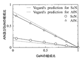
- Figure 4 shows an example of the relationship between Sc q Al z Ga 1-q -z GaN composition ratio in N and AlN and ScN composition ratio of GaN and lattice matching.
- the composition ratio calculated according to Vegard's law is indicated by a dotted line
- the composition ratio calculated by the first principle calculation is indicated by a solid line.
- the composition ratio according to the first principle calculation was different from the composition ratio according to the Vegard law.
- the composition of the ScN and AlN which Sc q Al z Ga 1-q -z N is GaN lattice matching
- Sc q Al z Ga 1- qz N does not contain GaN
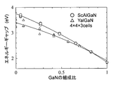
- Figure 5 shows the relationship between the GaN composition ratio, and Y q Al z Ga 1-q -z N and Sc q Al each band gap of the z Ga 1-q-z N ( energy gap).
- the band gap is a band gap at the ⁇ (gamma) point of the Brillouin zone.
- the calculation method of the band gap is the same as the calculation method of the band gap shown in FIG.
- the band gap of Sc q Al z Ga 1-qz N is also minimum, so that it is the same as Y q Al z Ga 1-qz N
- the band gap of Sc q Al z Ga 1-qz N with a GaN composition ratio of 0 is larger than the band gap of GaN. Therefore, in the semiconductor substrate 100 in which the second epitaxial crystal layer 130 is composed of Sc q Al z Ga 1-qz N (where the composition ratio of GaN is 0), there is a band offset at the interface between the channel and the Schottky layer. Therefore, the gate leakage current can be suppressed.
- Sc q Al z Ga 1-qz N has a larger band gap than Y q Al z Ga 1-qz N over a wide range of the GaN composition ratio. .
- Figure 6 shows a GaN composition ratio, the relationship between the respective amount of spontaneous polarization of Y q Al z Ga 1-q -z N and Sc q Al z Ga 1-q -z N.
- the amount of spontaneous polarization was calculated by the first principle calculation.
- Sc q Al z Ga 1-qz N has a larger spontaneous polarization amount than Y q Al z Ga 1-qz N over a wide range of the GaN composition ratio.
- the efficiency of optical transition in an optical device, the concentration of a two-dimensional electron gas in an electronic device, and the like are affected by the amount of polarization, but as shown in FIG. 6, M q Al z Ga 1-qz N
- the amount of spontaneous polarization can also be adjusted by selecting M in.
- the configuration of the semiconductor substrate 100 illustrated in FIG. 1 includes various modifications.
- the first epitaxial crystal layer 120 is In x Al y Ga 1-x -y N ( However, 0 ⁇ x ⁇ 1,0 ⁇ y ⁇ 1) is
- the second epitaxial crystal layer 130 is M q Al z Ga 1 ⁇ q ⁇ z N
- a spacer layer may be provided between the first epitaxial crystal layer 120 and the second epitaxial crystal layer 130.
- the spacer layer may be AlN. That is, the semiconductor substrate 100 is shown in M q Al z Ga 1-q -z N / AlN / In x Al y Ga 1-x-y N ( However, 0 ⁇ x ⁇ 1,0 ⁇ y ⁇ 1) You may have a structure. Since the semiconductor substrate 100 has AlN at the interface between the first epitaxial crystal layer 120 and the second epitaxial crystal layer 130, alloy scattering of channel electrons is suppressed, so that electron mobility is improved.
- M q1 Al z1 Ga 1-q1 -z1 N may have a larger lattice constant than M q2 Al z2 Ga 1-q2 -z2 N. Since M q1 Al z1 Ga 1-q1 -z1 N has a larger lattice constant than M q2 Al z2 Ga 1 -q2 -z2 N, the interface between the first epitaxial crystal layer 120 and the second epitaxial crystal layer 130 is formed. Since the generated piezoelectric polarization is relaxed, the threshold voltage of the HEMT formed using the semiconductor substrate 100 can be shifted to the plus side when the carriers are electrons, and to the minus side when the carriers are holes.
- the second epitaxial crystal layer 130 includes an M q Al z Ga 1-qz N layer in contact with the first epitaxial crystal layer 120, an InGaN layer in contact with the M q Al z Ga 1-qz N layer, A p-type InGaN layer in contact with the InGaN layer may be included. That is, the semiconductor substrate 100, p-type In x1 Ga 1-x1 N / In x2 Ga 1-x2 N / M q Al z Ga 1-q-z N / In x Al y Ga 1-x-y N ( provided that , 0 ⁇ x ⁇ 1, 0 ⁇ y ⁇ 1).
- the semiconductor substrate 100 Since the semiconductor substrate 100 has the above-described configuration, two-dimensional hole gas accumulates at the interface between the In x2 Ga 1-x2 N layer and the M q Al z Ga 1-qz N layer, and M q Al z Ga Two-dimensional electron gas is accumulated at the interface between the 1-q-z N layer and the In x Al y Ga 1-xy N layer (where 0 ⁇ x ⁇ 1, 0 ⁇ y ⁇ 1). Therefore, by using the semiconductor substrate 100, a complementary transistor having a p-channel transistor and an n-channel transistor can be formed in one chip.
- the semiconductor substrate 100 may further include an M q3 Al z2 Ga 1-q3-z2 N layer between the base substrate 110 and the first epitaxial crystal layer 120. That is, the semiconductor substrate 100, M q1 Al z1 Ga 1- q1-z1 N / In x Al y Ga 1-x-y N ( However, 0 ⁇ x ⁇ 1,0 ⁇ y ⁇ 1) / M q3 Al z3 You may have the structure shown by Ga1-q3-z3N .
- the In x Al y Ga 1-xy N layer (where 0 ⁇ x ⁇ 1, 0 ⁇ y ⁇ 1) is composed of the M q1 Al z1 Ga 1-q1-z1 N layer and the M q3 Al z3 Ga 1-q3 -Lattice matching or pseudo- lattice matching with at least one of the z3 N layers.
- the concentration of the two-dimensional carrier gas is increased.
- element resistance, pinch-off, and mutual conductance characteristics are improved.
- the second epitaxial crystal layer 130 is provided on the M q Al z Ga 1-qz N layer provided on the first epitaxial crystal layer 120 and the M q Al z Ga 1-qz N layer. And a p-type M q Al z Ga 1-qz N layer. That is, the semiconductor substrate 100, p-type M q Al z Ga 1-q -z N / M q Al z Ga 1-q-z N / In x Al y Ga 1-x-y N ( However, 0 ⁇ x ⁇ 1, 0 ⁇ y ⁇ 1).
- the semiconductor substrate 100 having this configuration since holes are injected into the first epitaxial crystal layer 120, an In x Al y Ga 1-xy N layer (where 0 ⁇ x ⁇ 1, 0 ⁇ y ⁇ 1) ) And the M q Al z Ga 1-qz N layer, the concentration of the two-dimensional electron gas generated at the interface can be improved. Therefore, the resistance of an element formed using the semiconductor substrate 100 can be reduced.
- the semiconductor substrate 100 may include an InGaN layer as the uppermost layer.
- an ohmic electrode can be formed in an InGaN layer having a small band gap where a channel is formed, so that contact resistance can be reduced.
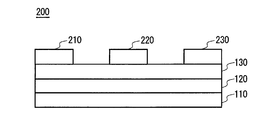
- FIG. 7 shows a structural example of the transistor 200 formed using the semiconductor substrate 100.
- the transistor 200 is, for example, a HEMT.
- the transistor 200 includes a source electrode 210, a gate electrode 220, and a drain electrode 230 formed on the second epitaxial crystal layer 130 in the semiconductor substrate 100.
- the source electrode 210 and the drain electrode 230 are Ti / Al, and the gate electrode 220 is Ni / Al.
- the source electrode 210, the gate electrode 220, and the drain electrode 230 are formed by, for example, a lithography method after a metal is stacked by an electron beam evaporation method.
- a two-dimensional carrier gas is generated between the first epitaxial crystal layer 120 and the second epitaxial crystal layer 130.
- Carriers injected from the source electrode 210 move to the drain electrode 230 using the two-dimensional carrier gas as a channel. Since the band gap of the first epitaxial crystal layer 120 is larger than that of the base substrate 110 and carriers are less likely to move between the gate electrode 220 and the first epitaxial crystal layer 120, the gate leakage current of the transistor 200 compared to the conventional HEMT. Is reduced.
- the transistor 200 since the second epitaxial crystal layer 130 is lattice-matched or pseudo-lattice-matched with the first epitaxial crystal layer 120, two-dimensional carrier gas due to piezoelectric charges is not generated. Therefore, the transistor 200 can realize a high threshold.
- the threshold voltage can be set to 0 V or more, a normally-off operation can be performed, and piezo breakdown is unlikely to occur.
Landscapes
- Junction Field-Effect Transistors (AREA)
Abstract
ベース基板と、ベース基板上に設けられた、IIIa族元素を含む窒化物の第1結晶からなる第1エピタキシャル結晶層と、第1エピタキシャル結晶層上に設けられ、第1結晶よりも大きなバンドギャップを有し、かつ、IIIa族元素及びIIIa族元素の一部を置換したIIIb族元素を含む窒化物の第2結晶からなる第2エピタキシャル結晶層とを備える半導体基板を提供する。上記の半導体基板において、第2エピタキシャル結晶層は、第1エピタキシャル結晶層に格子整合又は疑格子整合してもよい。
Description
本発明は、トランジスタ用半導体基板、トランジスタ及びトランジスタ用半導体基板の製造方法に関する。
窒化ガリウム系半導体結晶からなるHigh Electron Mobility Transistor(HEMT)の一形態として、ショットキー層がAlGaNからなり、チャネル層がInGaNまたはGaNからなるものが知られている(以下においてこの形態をAlGaN/GaN HEMTと呼称することがある)。AlGaN/GaN HEMTではゲートからのリーク電流が大きい。特にノーマリオフ動作(閾値電圧が>0)するモードのデバイスでは、AlGaN層と(In)GaN層のヘテロ界面にかかる電界が順方向となるため、その分リーク電流も増大する。
リーク電流を低減するべく、AlGaN層の厚みを大きくしてショットキー層の抵抗を増加させる方法、および、AlGaN層におけるAlの組成比を増大させることでGaN層あるいはInGaN層との間のバンドギャップ差を大きくする方法が知られている。また、AlGaN層とゲートの間に絶縁層を配置することにより、リーク電流を小さくするMetal-Insulator-Semiconductor HEMT(MIS-HEMT)も知られている(例えば、非特許文献1参照)。
非特許文献1 H. Sazawa et al., physica status solidi (c), 4, (2007)2748
非特許文献1 H. Sazawa et al., physica status solidi (c), 4, (2007)2748
AlGaN/GaN HEMTにおいては、AlGaNショットキー層とGaN層またはInGaN層との間の格子定数の差に起因して、AlGaN層にピエゾ分極が発生する。ピエゾ分極が発生すると、当該ピエゾ分極を打ち消すべく、ヘテロ界面のGaN層側またはInGaN層側に2次元電子ガスが発生する。
ピエゾ分極はAlGaN層の厚み及びAlの組成比が増大すればするほど大きくなり、それに応じ、2次元電子ガスの濃度も増大する。その結果、HEMTの閾値はマイナス側にシフトする。すなわちAlGaN/GaNへテロ構造を有するHEMTにおいては、リーク電流の発生を抑制することと、高い閾値を実現することを両立することが困難であった。このため、リーク電流が小さく、且つ、ノーマリオフ動作するHEMTの作製は困難であった。
AlGaN層とゲートとの間に絶縁層が配置されたMIS-HEMTにおいては、ノーマリオフ動作とリーク電流の抑制とを両立することができる。しかし、MIS-HEMTを製造するには、絶縁層の形成が必要になるので、製造コストが増大する。また、MIS-HEMTは、AlGaN層とゲートの間に絶縁層を有するので、閾値のばらつきがショットキー型のHEMTよりも大きいという問題がある。また、絶縁膜とAlGaN層の界面に発生する界面準位密度を低く抑えることが難しく、デバイスの特性がヒステリシスを示しやすいなどの問題がある。
AlGaN/GaN HEMTでは、AlGaNとGaNには大きな歪が内在している。そのため電界を印加した際に発生するピエゾ応力が加わることにより、両結晶は容易に弾性限界を超え、結晶が破壊される現象、いわゆるピエゾ破壊が起こりやすいという問題がある。
本発明の第1の態様においては、ベース基板と、ベース基板上に設けられた、IIIa族元素を含む窒化物の第1結晶からなる第1エピタキシャル結晶層と、第1エピタキシャル結晶層上に設けられ、第1結晶よりも大きなバンドギャップを有し、かつ、IIIa族元素及び当該IIIa族元素の一部を置換したIIIb族元素を含む窒化物の第2結晶からなる第2エピタキシャル結晶層とを備えるトランジスタ用半導体基板を提供する。上記の半導体基板において、第2エピタキシャル結晶層は、第1エピタキシャル結晶層に格子整合又は疑格子整合してもよい。
上記の半導体基板において、一例として、第1結晶はInxAlyGa1-x―yN(ただし、0≦x≦1、0≦y≦1)であり、第2結晶がMqAlzGa1-q―zNであり、Mはスカンジウム、イットリウム及びランタノイド系元素群の中から選ばれる一種以上の元素であり、0<q≦0.30、0<z<1、q+z≦1である。上記の第2結晶は、例えばYqAlzGa1-q―zN(0<q≦0.30、0<z<1、q+z≦1)である。また、第2エピタキシャル結晶層の導電型は、例えばn型又は絶縁型である。上記の第1結晶の一例としてGaNが挙げられ、この場合、MqAlzGa1-q―zNにおけるMがイットリウムまたはスカンジウムであり、q/zの値が0.1から0.35の範囲であることが好ましい。第1結晶又は第2結晶の結晶型は、ウルツ鉱型が好ましい。
本発明の第2の態様においては、第1の態様の半導体基板を備え、第1エピタキシャル結晶層と第2エピタキシャル結晶層との界面よりも第1エピタキシャル結晶層側に生成される2次元キャリアガスをチャネルとするトランジスタを提供する。上記のキャリアが電子である場合、結晶の上面側がIII族極性であってよく、上記のキャリアがホールである場合、V族極性であってよい。当該トランジスタは、ノーマリオフ動作できる。
本発明の第3の態様においては、ベース基板上に、IIIa族元素を含む窒化物の第1結晶をエピタキシャル成長させて第1エピタキシャル結晶層を形成する段階と、第1エピタキシャル結晶層上に、第1結晶よりも大きなバンドギャップを有し、かつ、IIIa族元素及び当該IIIa族元素の一部を置換したIIIb族元素を含む窒化物の第2結晶をエピタキシャル成長させて、第2エピタキシャル結晶層を形成する段階とを備えるトランジスタ用半導体基板の製造方法を提供する。
なお、本明細書において、IIIa族とはホウ素族を指し、IIIb族とはスカンジウム族を指す。なお、IIIa族およびIIIb族は、旧CAS方式における名称である。
図1は、本発明の一実施形態に係る半導体基板100の断面を示す。半導体基板100は、ベース基板110、第1エピタキシャル結晶層120及び第2エピタキシャル結晶層130を備える。ベース基板110は、例えば、Al2O3、Si、SiC、ZnO、又はGaNからなる基板である。第1エピタキシャル結晶層120は、IIIa族元素を含む窒化物の第1結晶から構成される。第1エピタキシャル結晶層120を構成する第1結晶は、例えばInxAlyGa1-x―yN(ただし、0≦x≦1、0≦y≦1)である。
第2エピタキシャル結晶層130は、第1エピタキシャル結晶層120上に設けられている。第2エピタキシャル結晶層130は、第1結晶よりも大きなバンドギャップを有する第2結晶で構成される。第2エピタキシャル結晶層130を構成する第2結晶は、例えば、IIIa族元素及び当該IIIa族元素の一部を置換したIIIb族元素を含む窒化物である。一例として、第1結晶に含まれるIIIa族元素と、第2結晶に含まれるIIIa族元素とにおいて、少なくとも1種類のIIIa族元素は共通しない。また、第1結晶および第2結晶は、共通するIIIa族元素を含んでもよい。例えば第1結晶は、IIIa族元素としてInおよびAlを含み、第2結晶は、IIIa族元素としてAlを含みInを含まない。また、第1結晶に含まれるIIIa族元素と、第2結晶に含まれるIIIa族元素とにおいて、共通するIIIa族元素の組成比が異なってよい。第2エピタキシャル結晶層130を構成する第2結晶は、例えばMqAlzGa1-q―zNである。ただし、Mはスカンジウム、イットリウム及びランタノイド系元素群の中から選ばれる一種以上の元素であり、0<q≦0.30、0<z<1、q+z≦1である。
第2エピタキシャル結晶層130におけるIIIa族元素の一部をIIIb族元素で置換することで、第1エピタキシャル結晶層120と第2エピタキシャル結晶層130との格子定数差を低減できる。その結果、ピエゾ分極により発生する2次元キャリアガスの濃度が減少し、半導体基板100を用いて形成されるHEMTの閾値はキャリアが電子の場合プラス側にシフトし、ホールの場合マイナス側にシフトする。結果としてトランジスタをノーマリオフ動作させることができる。
具体的には、第2エピタキシャル結晶層130は、IIIa族元素及びIIIb族元素をさまざまな比率で含む窒化物であってよい。例えば、第2エピタキシャル結晶層130は、IIIa族元素及びIIIb族元素を(0.70~0.95):(0.30~0.05)の比率で有する。第1エピタキシャル結晶層120がGaN層である場合、第2エピタキシャル結晶層130においてMで示されるIIIb族元素と、Alとの組成比q/zは、0.1から0.25の範囲であってよい。また、組成比q/zは、0.1から0.35の範囲であってもよい。第2エピタキシャル結晶層130の導電型は、n型又は半絶縁型であってよい。
第2エピタキシャル結晶層130を構成する第2結晶は、第1エピタキシャル結晶層120を構成する第1結晶よりも大きなバンドギャップを有する。したがって、第2エピタキシャル結晶層130は、第1エピタキシャル結晶層120及び第2エピタキシャル結晶層130の積層方向におけるキャリアの移動を抑制する。その結果、半導体基板100を用いて形成されるHEMTにおけるゲートリーク電流を抑制することができ、また、ピエゾ破壊を防ぐことができる。
第2エピタキシャル結晶層130は、第1エピタキシャル結晶層120に格子整合又は擬格子整合することが好ましい。ここで、本明細書における「擬格子整合」とは、完全な格子整合ではないが、互いに接する2つの半導体の格子定数の差が小さく、格子不整合による欠陥の発生が顕著でない範囲で、互いに接する2つの半導体を積層できる状態をいう。このとき、各半導体の結晶格子が、弾性変形できる範囲内で変形することで、上記格子定数の差が吸収される。例えば、第1エピタキシャル結晶層120と第2エピタキシャル結晶層130との格子緩和限界厚さ内での積層状態は、擬格子整合した状態である。
上述したように、一例として、第1エピタキシャル結晶層120はInxAlyGa1-x―yN(ただし、0≦x≦1、0≦y≦1)である。第2エピタキシャル結晶層130はMqAlzGa1-q―zNである。ここで、Mはスカンジウム、イットリウム及びランタノイド系元素群の中から選ばれる一種以上の元素である。これらの内、イットリウム、ユーロピウムがMとして好ましく、イットリウムがさらに好ましい。q及びzは、0<q≦0.30、0<z<1、q+z≦1の関係を満たす。q及びzの間の関係は、q≦zであってもよい。
第2エピタキシャル結晶層130が上記の条件を満たすMqAlzGa1-q―zNで構成される場合には、第2エピタキシャル結晶層130は、InxAlyGa1-x―yN(ただし、0≦x≦1、0≦y≦1)からなる第1エピタキシャル結晶層120に格子整合又は擬格子整合する。第2エピタキシャル結晶層130が第1エピタキシャル結晶層120に格子整合又は擬格子整合する場合には、第1エピタキシャル結晶層120及び第2エピタキシャル結晶層130にピエゾ分極が発生しない。第1エピタキシャル結晶層120がInxAlyGa1-x―yN(ただし、0≦x≦1、0≦y≦1)である場合には、第2エピタキシャル結晶層130は、YqAlzGa1-q―zN(0<q≦0.30、0<z<1、q+z≦1)であることが好ましい。
第1エピタキシャル結晶層120及び第2エピタキシャル結晶層130にピエゾ分極が発生しない場合には、第1エピタキシャル結晶層120と第2エピタキシャル結晶層130との間にピエゾ電荷が発生しない。したがって、第1エピタキシャル結晶層120及び第2エピタキシャル結晶層130にピエゾ分極が発生する場合に比べて、第1エピタキシャル結晶層120と第2エピタキシャル結晶層130との間に生成される2次元キャリアガスの濃度が低下する。
第1エピタキシャル結晶層120と第2エピタキシャル結晶層130との間の2次元キャリアガスの濃度が低下すると、当該2次元キャリアガスをチャネルとするHEMTにおける閾値電圧を、キャリアが電子の場合プラス側に、ホールの場合マイナス側にシフトさせることができる。なお、当該HEMTは、半導体基板100を用いて形成され、第1エピタキシャル結晶層120と第2エピタキシャル結晶層130との間の2次元キャリアガスをチャネルとする。このように、第2エピタキシャル結晶層130が、IIIa族元素及び当該IIIa族元素を置換したIIIb族元素を有する窒化物であることで、半導体基板100を用いて形成されるHEMTをノーマリオフ動作させることができる。このため、ピエゾ破壊耐性の高いHEMTを構成することができる。
ここで、ベガード則によれば、合金の格子定数と組成元素の濃度との間には比例関係が成り立つ。YqAlzGa1-q―zNの格子定数をaYAlGaN、YNの格子定数をaYN、AlNの格子定数をaAlN、GaNの格子定数をaGaNとすると、aYAlGaN=aYN・q+aAlN・z+aGaN(1-qx-z)の関係が成り立つ。
aYN=3.99(Å)、aAlN=3.07(Å)、aGaN=3.18(Å)であることが知られているので、上記の関係式を用いると、q=0.11、z=0.89の場合にaYAlGaN=3.17(Å)となり、YqAlzGa1-q―zNの格子定数がGaNの格子定数と略等しくなる。つまり、上記の格子定数を用いると、Y0.11Al0.89Nの格子定数はGaNの格子定数に等しい。
図2は、ベガード則に則って算出したGaNと格子整合するYqAlzGa1-q―zNにおけるGaNの組成比とAlN及びYNの組成比との関係の一例を示す。図2によれば、YqAlzGa1-q―zNにGaNが含まれない場合には、YNとAlNとの組成比が0.14:0.86(つまり、q/z=0.14/0.86)であれば、YqAlzGa1-q―zNがGaNに格子整合することがわかる。
ただし、実際の結晶においては、結晶中の原子の配列、局所的な組成の揺らぎ、同族元素の秩序化、格子間不純物及び各種欠陥などの影響により、格子定数は微妙に変化する。格子定数を正確に見積もるには、これらの要因を考慮した第一原理計算を使用できる。YNは、結晶形が岩塩構造の場合が最も安定であるが、ウルツ鉱型であるAlGaN又はGaNとYNとの混晶であるYAlGaNは、ウルツ鉱構造とすることが好ましい。
YNはAlNあるいはGaNに比べ、共有結合性が弱く、イオン結合性が強い。したがって、YNとGaN、YNとAlN、又はYNとAlGaNの混晶は、YNを含まない結晶に比べてバンドギャップが大きい。
図3は、GaNの組成比とYqAlzGa1-q―zN(q:z=11:89)のバンドギャップとの関係を示す。バンドギャップは、ブリルアンゾーンのΓ(ガンマ)点におけるバンドギャップである。バンドギャップは、密度汎関数理論に基づく第一原理計算により求めた。イオン-電子相互作用は、ウルトラ疑ポテンシャルで記述した。交換相関エネルギーは一般化勾配近似を適用した。
図3から明らかなように、GaNの組成比が1の場合にYqAlzGa1-q―zN(q:z=11:89)のエネルギーギャップが最小となるので、YqAlzGa1-q―zN(q:z=11:89)のバンドギャップは、GaNのバンドギャップよりも大きい。したがって、第2エピタキシャル結晶層130がYqAlzGa1-q―zN(q:z=11:89)で構成された半導体基板100では、チャネルとショットキー層界面にはバンドオフセットが存在するため、ゲートリーク電流を抑制することができる。
一方、前述の通り、本HEMTではチャネル層とショットキー層が格子整合しているため、ピエゾ分極に起因するチャネル電荷が発生しない状態である。このため本HEMTでは高い閾値が実現でき、ノーマリオフ動作可能である。すなわち本HEMTでは、AlGaN/GaN HEMTに見られた、ゲートリークと高い閾値のトレードオフが回避される。
以上のとおり、半導体基板100が、IIIa族元素を含む窒化物の第1結晶からなる第1エピタキシャル結晶層120と、第1結晶よりも大きなバンドギャップを有し、かつ、IIIa族元素及びIIIb族元素を含む窒化物の第2結晶からなる第2エピタキシャル結晶層130とを備えることにより、半導体基板100を用いて形成されるHEMTのリーク電流が低減するとともに、閾値をプラス側にシフトできる。このため、当該HEMTにノーマリオフ動作をさせることができる。
半導体基板100は、公知のエピタキシャル結晶成長法を用いて製造することができる。例えば、GaNからなるベース基板110を反応炉に載置した後に、MOCVD法(有機金属気相成長法)を用いることにより、InxAlyGa1-x―yN(ただし、0≦x≦1、0≦y≦1)からなる第1エピタキシャル結晶層120を形成することができる。次に、第1エピタキシャル結晶層120の上にYqAlzGa1-q―zNからなる第2エピタキシャル結晶層130を形成することができる。具体的には、ベース基板110を載置した反応炉に、N源としてのアンモニア、Al源としてのトリメチルアルミニウム及びY源としてトリスシクロペンタジエニルイットリウムを導入して加熱することにより、YqAlzGa1-q―zNを第1エピタキシャル結晶層120上に形成することができる。
図4は、GaNと格子整合するScqAlzGa1-q―zNにおけるGaNの組成比とAlN及びScNの組成比との関係の一例を示す。なお図4においては、ベガード則に沿って算出した組成比を点線で示し、第一原理計算によって算出した組成比を実線で示す。図4に示すように、第一原理計算による組成比は、ベガード則による組成比とは異なる値になった。
図4に示すように、ScqAlzGa1-q―zNにGaNが含まれない場合に、ScqAlzGa1-q―zNがGaNと格子整合するScNとAlNとの組成比をベガード則に沿って算出すると、概ね0.16:0.84(つまり、q/z=0.16/0.84)になる。同様に、ScqAlzGa1-q―zNにGaNが含まれない場合に、ScqAlzGa1-q―zNがGaNと格子整合するScNとAlNとの組成比を第一原理計算に沿って算出すると、概ね0.23:0.77(つまり、q/z=0.23/0.77)になる。
図5は、GaNの組成比と、YqAlzGa1-q―zNおよびScqAlzGa1-q―zNのそれぞれのバンドギャップ(エネルギーギャップ)との関係を示す。バンドギャップは、ブリルアンゾーンのΓ(ガンマ)点におけるバンドギャップである。当該バンドギャップの算出方法は、図3に示したバンドギャップの算出方法と同様である。
図5から明らかなように、GaNの組成比が1の場合にScqAlzGa1-q―zNのバンドギャップも最小となるので、YqAlzGa1-q―zNと同様に、GaNの組成比が0のScqAlzGa1-q―zNのバンドギャップは、GaNのバンドギャップよりも大きい。したがって、第2エピタキシャル結晶層130がScqAlzGa1-q―zN(但し、GaNの組成比は0)で構成された半導体基板100では、チャネルとショットキー層界面にはバンドオフセットが存在するため、ゲートリーク電流を抑制することができる。また、図5に示すように、GaN組成比の広い範囲に渡って、ScqAlzGa1-q―zNのほうが、YqAlzGa1-q―zNよりもバンドギャップが大きい。
図6は、GaNの組成比と、YqAlzGa1-q―zNおよびScqAlzGa1-q―zNのそれぞれの自発分極量との関係を示す。図6においても図3と同様に、自発分極量を第一原理計算により算出した。図6に示すように、GaN組成比の広い範囲に渡って、ScqAlzGa1-q―zNのほうが、YqAlzGa1-q―zNよりも自発分極量が大きい。
一般に、光学デバイスにおける光学遷移の効率、および、電子デバイスにおける二次元電子ガスの濃度等は、分極量の影響を受けるが、図6に示すように、MqAlzGa1-q―zNにおけるMを選択することによっても、自発分極量を調整することができる。
図1に示した半導体基板100の構成は、さまざまな変形例を含む。例えば、第1エピタキシャル結晶層120がInxAlyGa1-x―yN(ただし、0≦x≦1、0≦y≦1)であり、第2エピタキシャル結晶層130がMqAlzGa1-q―zNであり、第1エピタキシャル結晶層120と第2エピタキシャル結晶層130との間にスペーサ層を有しても良い。スペーサ層はAlNであっても良い。つまり、半導体基板100は、MqAlzGa1-q―zN/AlN/InxAlyGa1-x―yN(ただし、0≦x≦1、0≦y≦1)で示される構成を有してもよい。半導体基板100が、第1エピタキシャル結晶層120と第2エピタキシャル結晶層130との界面にAlNを有することにより、チャネル電子の合金散乱が抑制されるので、電子移動度が向上する。
第2エピタキシャル結晶層130は、第1エピタキシャル結晶層120上に設けられたMq2Alz2Ga1-q2―z2N層と、当該Mq2Alz2Ga1-q2―z2N層上に設けられたMq1Alz1Ga1-q1―z1N層とを有してもよい。つまり、半導体基板100は、Mq1Alz1Ga1-q1―z1N/Mq2Alz2Ga1-q2―z2N/InxAlyGa1-x―yN(ただし、0≦x≦1、0≦y≦1)で示される構成を有してもよい。
Mq1Alz1Ga1-q1―z1NがMq2Alz2Ga1-q2―z2Nよりも大きな格子定数を有してもよい。Mq1Alz1Ga1-q1―z1NがMq2Alz2Ga1-q2―z2Nよりも大きな格子定数を有することにより、第1エピタキシャル結晶層120と第2エピタキシャル結晶層130との界面に生じるピエゾ分極が緩和されるので、半導体基板100を用いて形成されるHEMTの閾値電圧を、キャリアが電子の場合プラス側に、ホールの場合マイナス側にシフトさせることができる。
第2エピタキシャル結晶層130は、第1エピタキシャル結晶層120に接するMqAlzGa1-q―zN層と、当該MqAlzGa1-q―zN層に接するInGaN層と、当該InGaN層に接するp型InGaN層とを有してもよい。つまり、半導体基板100は、p型Inx1Ga1-x1N/Inx2Ga1-x2N/MqAlzGa1-q―zN/InxAlyGa1-x―yN(ただし、0≦x≦1、0≦y≦1)で示される構成を有してよい。
半導体基板100が上記の構成を有することにより、Inx2Ga1-x2N層とMqAlzGa1-q―zN層との界面に2次元ホールガスが蓄積し、MqAlzGa1-q―zN層とInxAlyGa1-x―yN層(ただし、0≦x≦1、0≦y≦1)との界面に2次元電子ガスが蓄積される。したがって、半導体基板100を用いることにより、pチャネルのトランジスタとnチャネルのトランジスタとを有する相補型トランジスタを1チップで構成することができる。
半導体基板100は、ベース基板110と第1エピタキシャル結晶層120との間にMq3Alz2Ga1-q3―z2N層をさらに備えてもよい。つまり、半導体基板100は、Mq1Alz1Ga1-q1―z1N/InxAlyGa1-x―yN(ただし、0≦x≦1、0≦y≦1)/Mq3Alz3Ga1-q3―z3Nで示される構成を有してもよい。InxAlyGa1-x―yN層(ただし、0≦x≦1、0≦y≦1)は、Mq1Alz1Ga1-q1―z1N層及びMq3Alz3Ga1-q3―z3N層の少なくとも1つに格子整合又は擬格子整合する。
当該構成を有する半導体基板100においては、Mq1Alz1Ga1-q1―z1N層及びMq3Alz3Ga1-q3―z3N層からInxAlyGa1-x―yN層(ただし、0≦x≦1、0≦y≦1)にキャリアが供給されるので、2次元キャリアガスの濃度が高まる。その結果、半導体基板100を用いてトランジスタを形成すると、素子抵抗、ピンチオフ及び相互コンダクタンス特性が改善する。
第2エピタキシャル結晶層130は、第1エピタキシャル結晶層120上に設けられたMqAlzGa1-q―zN層と、当該MqAlzGa1-q―zN層上に設けられたp型MqAlzGa1-q―zN層とを有してもよい。つまり、半導体基板100は、p型MqAlzGa1-q―zN/MqAlzGa1-q―zN/InxAlyGa1-x―yN(ただし、0≦x≦1、0≦y≦1)で示される構成を有してもよい。当該構成を有する半導体基板100においては、第1エピタキシャル結晶層120にホールが注入されるので、InxAlyGa1-x―yN層(ただし、0≦x≦1、0≦y≦1)とMqAlzGa1-q―zN層との界面に発生する2次元電子ガスの濃度を向上させることができる。したがって、半導体基板100を用いて形成される素子の抵抗を下げることができる。
半導体基板100は、最上層にInGaN層を備えてもよい。当該構成を有する半導体基板100においては、チャネルが形成される、バンドギャップが小さいInGaN層にオーミック電極を形成することができるので、接触抵抗を低減することができる。
なお、上記の説明において、0<q≦0.30、0<z<1、q+z≦1、0<q1≦0.30、0<z1<1、q1+z1≦1、0<q2≦0.30、0<z2<1、q2+z2≦1、0<q3≦0.30、0<z3<1、q3+z3≦1、0≦x1≦0.10、0≦x2≦0.10、0≦x3≦0.50である。
図7は、半導体基板100を用いて形成されたトランジスタ200の構成例を示す。トランジスタ200は、例えばHEMTである。トランジスタ200は、半導体基板100における第2エピタキシャル結晶層130上に形成されたソース電極210、ゲート電極220及びドレイン電極230を備える。ソース電極210及びドレイン電極230は、Ti/Al、ゲート電極220はNi/Alである。ソース電極210、ゲート電極220及びドレイン電極230は、例えば、電子線蒸着法で金属を積層した後、リソグラフィー法により形成される。
トランジスタ200においては、第1エピタキシャル結晶層120と第2エピタキシャル結晶層130との間に2次元キャリアガスが生成される。ソース電極210から注入されたキャリアは、当該2次元キャリアガスをチャネルとしてドレイン電極230まで移動する。第1エピタキシャル結晶層120のバンドギャップがベース基板110よりも大きく、ゲート電極220と第1エピタキシャル結晶層120との間をキャリアが移動しにくいので、従来のHEMTに比べてトランジスタ200のゲートリーク電流は低減される。
また、トランジスタ200においては、第2エピタキシャル結晶層130が第1エピタキシャル結晶層120と格子整合又は擬格子整合するので、ピエゾ電荷による2次元キャリアガスが発生しない。したがって、トランジスタ200は高い閾値が実現できる。閾値電圧は0V以上とすることができ、ノーマリオフ動作をすることができ、また、ピエゾ破壊も起こしにくい。
以上、本発明を実施の形態を用いて説明したが、本発明の技術的範囲は上記実施の形態に記載の範囲には限定されない。上記実施の形態に、多様な変更または改良を加えることが可能であることが当業者に明らかである。その様な変更または改良を加えた形態も本発明の技術的範囲に含まれ得ることが、請求の範囲の記載から明らかである。
100 半導体基板、110 ベース基板、120 第1エピタキシャル結晶層、130 第2エピタキシャル結晶層、200 トランジスタ、210 ソース電極、220 ゲート電極、230 ドレイン電極
Claims (9)
- ベース基板と、
前記ベース基板上に設けられた、IIIa族元素を含む窒化物の第1結晶からなる第1エピタキシャル結晶層と、
前記第1エピタキシャル結晶層上に設けられ、前記第1結晶よりも大きなバンドギャップを有し、かつ、IIIa族元素及び前記IIIa族元素の一部を置換したIIIb族元素を含む窒化物の第2結晶からなる第2エピタキシャル結晶層と
を備えるトランジスタ用半導体基板。 - 前記第2エピタキシャル結晶層が、前記第1エピタキシャル結晶層に格子整合又は疑格子整合する請求項1に記載のトランジスタ用半導体基板。
- 前記第1結晶がInxAlyGa1-x―yN(ただし、0≦x≦1、0≦y≦1)であり、
前記第2結晶がMqAlzGa1-q―zNであり、
Mはスカンジウム、イットリウム及びランタノイド系元素群の中から選ばれる一種以上の元素であり、
0<q≦0.30、0<z<1、q+z≦1である請求項1に記載のトランジスタ用半導体基板。 - 前記第2エピタキシャル結晶層の導電型がn型又は絶縁型である請求項1に記載のトランジスタ用半導体基板。
- 前記第1結晶がGaNであり、
前記MqAlzGa1-q―zNにおけるMがイットリウムまたはスカンジウムであり、
q/zの値が0.1から0.35の範囲である請求項3に記載のトランジスタ用半導体基板。 - 前記第1結晶又は前記第2結晶の結晶構造がウルツ鉱型である請求項1に記載のトランジスタ用半導体基板。
- 請求項1に記載のトランジスタ用半導体基板を備え、
前記第1エピタキシャル結晶層と前記第2エピタキシャル結晶層との界面よりも前記第1エピタキシャル結晶層側に生成される2次元キャリアガスをチャネルとするトランジスタ。 - ノーマリオフ動作する請求項7に記載のトランジスタ。
- ベース基板上に、IIIa族元素を含む窒化物の第1結晶をエピタキシャル成長させて第1エピタキシャル結晶層を形成する段階と、
前記第1エピタキシャル結晶層上に、前記第1結晶よりも大きなバンドギャップを有し、かつ、IIIa族元素及び前記IIIa族元素の一部を置換したIIIb族元素を含む窒化物の第2結晶をエピタキシャル成長させて、第2エピタキシャル結晶層を形成する段階と
を備えるトランジスタ用半導体基板の製造方法。
Applications Claiming Priority (2)
| Application Number | Priority Date | Filing Date | Title |
|---|---|---|---|
| JP2011-140563 | 2011-06-24 | ||
| JP2011140563 | 2011-06-24 |
Publications (1)
| Publication Number | Publication Date |
|---|---|
| WO2012176411A1 true WO2012176411A1 (ja) | 2012-12-27 |
Family
ID=47422269
Family Applications (1)
| Application Number | Title | Priority Date | Filing Date |
|---|---|---|---|
| PCT/JP2012/003908 Ceased WO2012176411A1 (ja) | 2011-06-24 | 2012-06-14 | トランジスタ用半導体基板、トランジスタ及びトランジスタ用半導体基板の製造方法 |
Country Status (3)
| Country | Link |
|---|---|
| JP (1) | JP6001345B2 (ja) |
| TW (1) | TW201306257A (ja) |
| WO (1) | WO2012176411A1 (ja) |
Cited By (2)
| Publication number | Priority date | Publication date | Assignee | Title |
|---|---|---|---|---|
| EP3138118A4 (en) * | 2014-05-02 | 2017-09-13 | Translucent, Inc. | III-N MATERIAL GROWN ON ErAIN BUFFER ON Si SUBSTRATE |
| CN108615756A (zh) * | 2018-06-15 | 2018-10-02 | 苏州汉骅半导体有限公司 | 半导体器件 |
Families Citing this family (4)
| Publication number | Priority date | Publication date | Assignee | Title |
|---|---|---|---|---|
| EP2779213B1 (en) * | 2013-03-12 | 2015-05-06 | Siltronic AG | Semiconductor wafer with a layer of AlzGa1-zN and process for producing it |
| JP2021027151A (ja) * | 2019-08-05 | 2021-02-22 | 富士通株式会社 | 半導体装置、半導体装置の製造方法及び増幅器 |
| JP7835504B2 (ja) * | 2021-02-12 | 2026-03-25 | レイセオン カンパニー | 希土類iii族窒化物n極性hemt |
| EP4407657A4 (en) * | 2021-09-21 | 2025-08-20 | Shin Etsu Handotai Co Ltd | NITRIDE SEMICONDUCTOR SUBSTRATE AND PROCESS FOR PRODUCING THE SAME |
Citations (6)
| Publication number | Priority date | Publication date | Assignee | Title |
|---|---|---|---|---|
| JPH1154840A (ja) * | 1997-07-30 | 1999-02-26 | Toshiba Corp | 半導体発光装置 |
| JP2000243947A (ja) * | 1999-02-19 | 2000-09-08 | Sharp Corp | 窒化物系化合物半導体装置 |
| JP2001060682A (ja) * | 1999-08-19 | 2001-03-06 | Sharp Corp | 半導体装置 |
| JP2007305954A (ja) * | 2006-03-27 | 2007-11-22 | Nichia Chem Ind Ltd | 電界効果トランジスタ及びその装置 |
| JP2008047859A (ja) * | 2006-08-21 | 2008-02-28 | Samsung Electro Mech Co Ltd | 窒化物半導体発光素子 |
| JP2011515861A (ja) * | 2008-03-25 | 2011-05-19 | ピコギガ インターナショナル | 窒化ガリウムまたはガリウムおよびアルミニウム窒化物の層を製造する方法 |
Family Cites Families (2)
| Publication number | Priority date | Publication date | Assignee | Title |
|---|---|---|---|---|
| JP3209270B2 (ja) * | 1999-01-29 | 2001-09-17 | 日本電気株式会社 | ヘテロ接合電界効果トランジスタ |
| JP2009182054A (ja) * | 2008-01-29 | 2009-08-13 | Sumitomo Electric Ind Ltd | 半導体装置、基板、半導体装置の製造方法および基板の製造方法 |
-
2012
- 2012-06-14 WO PCT/JP2012/003908 patent/WO2012176411A1/ja not_active Ceased
- 2012-06-19 JP JP2012138060A patent/JP6001345B2/ja active Active
- 2012-06-21 TW TW101122169A patent/TW201306257A/zh unknown
Patent Citations (6)
| Publication number | Priority date | Publication date | Assignee | Title |
|---|---|---|---|---|
| JPH1154840A (ja) * | 1997-07-30 | 1999-02-26 | Toshiba Corp | 半導体発光装置 |
| JP2000243947A (ja) * | 1999-02-19 | 2000-09-08 | Sharp Corp | 窒化物系化合物半導体装置 |
| JP2001060682A (ja) * | 1999-08-19 | 2001-03-06 | Sharp Corp | 半導体装置 |
| JP2007305954A (ja) * | 2006-03-27 | 2007-11-22 | Nichia Chem Ind Ltd | 電界効果トランジスタ及びその装置 |
| JP2008047859A (ja) * | 2006-08-21 | 2008-02-28 | Samsung Electro Mech Co Ltd | 窒化物半導体発光素子 |
| JP2011515861A (ja) * | 2008-03-25 | 2011-05-19 | ピコギガ インターナショナル | 窒化ガリウムまたはガリウムおよびアルミニウム窒化物の層を製造する方法 |
Cited By (2)
| Publication number | Priority date | Publication date | Assignee | Title |
|---|---|---|---|---|
| EP3138118A4 (en) * | 2014-05-02 | 2017-09-13 | Translucent, Inc. | III-N MATERIAL GROWN ON ErAIN BUFFER ON Si SUBSTRATE |
| CN108615756A (zh) * | 2018-06-15 | 2018-10-02 | 苏州汉骅半导体有限公司 | 半导体器件 |
Also Published As
| Publication number | Publication date |
|---|---|
| TW201306257A (zh) | 2013-02-01 |
| JP6001345B2 (ja) | 2016-10-05 |
| JP2013030763A (ja) | 2013-02-07 |
Similar Documents
| Publication | Publication Date | Title |
|---|---|---|
| JP6473017B2 (ja) | 化合物半導体基板 | |
| JP6002508B2 (ja) | 窒化物半導体ウェハ | |
| JP5810293B2 (ja) | 窒化物半導体装置 | |
| KR101124937B1 (ko) | 질화물계 트랜지스터를 위한 캡층 및/또는 패시베이션층,트랜지스터 구조 및 그 제조방법 | |
| JP5718458B2 (ja) | 電界効果トランジスタ及び半導体装置 | |
| CN107068749B (zh) | 在异质基底上的第III族氮化物缓冲层结构的p型掺杂 | |
| US8344422B2 (en) | Semiconductor device | |
| US8653561B2 (en) | III-nitride semiconductor electronic device, and method of fabricating III-nitride semiconductor electronic device | |
| US7985984B2 (en) | III-nitride semiconductor field effect transistor | |
| US20120299060A1 (en) | Nitride semiconductor device and manufacturing method thereof | |
| JP6001345B2 (ja) | トランジスタ用半導体基板、トランジスタ及びトランジスタ用半導体基板の製造方法 | |
| WO2011024754A1 (ja) | Iii族窒化物半導体積層ウェハ及びiii族窒化物半導体デバイス | |
| US12224339B2 (en) | High electron mobility transistor | |
| US10332975B2 (en) | Epitaxial substrate for semiconductor device and method for manufacturing same | |
| US20130043492A1 (en) | Nitride semiconductor transistor | |
| JP5344445B2 (ja) | 半導体素子 | |
| WO2010058561A1 (ja) | 電界効果トランジスタ | |
| US20150048418A1 (en) | Semiconductor power device | |
| US9331169B2 (en) | Nitride semiconductor Schottky diode and method for manufacturing same | |
| JP2013038157A (ja) | 化合物半導体基板 | |
| JP6084254B2 (ja) | 化合物半導体基板 | |
| JP2019067786A (ja) | 高出力素子 | |
| JP2012204512A (ja) | 半導体装置 | |
| JP2017005223A (ja) | 光電変換装置 | |
| WO2015152411A1 (ja) | 窒化物半導体装置およびその製造方法、ならびにダイオードおよび電界効果トランジスタ |
Legal Events
| Date | Code | Title | Description |
|---|---|---|---|
| 121 | Ep: the epo has been informed by wipo that ep was designated in this application |
Ref document number: 12802321 Country of ref document: EP Kind code of ref document: A1 |
|
| NENP | Non-entry into the national phase |
Ref country code: DE |
|
| 122 | Ep: pct application non-entry in european phase |
Ref document number: 12802321 Country of ref document: EP Kind code of ref document: A1 |