WO2012173049A1 - アナログスイッチ回路及びこれを用いたモータ駆動装置 - Google Patents
アナログスイッチ回路及びこれを用いたモータ駆動装置 Download PDFInfo
- Publication number
- WO2012173049A1 WO2012173049A1 PCT/JP2012/064754 JP2012064754W WO2012173049A1 WO 2012173049 A1 WO2012173049 A1 WO 2012173049A1 JP 2012064754 W JP2012064754 W JP 2012064754W WO 2012173049 A1 WO2012173049 A1 WO 2012173049A1
- Authority
- WO
- WIPO (PCT)
- Prior art keywords
- analog switch
- voltage
- phase
- resistor
- motor
- Prior art date
- Legal status (The legal status is an assumption and is not a legal conclusion. Google has not performed a legal analysis and makes no representation as to the accuracy of the status listed.)
- Ceased
Links
Images





Classifications
-
- H—ELECTRICITY
- H03—ELECTRONIC CIRCUITRY
- H03K—PULSE TECHNIQUE
- H03K17/00—Electronic switching or gating, i.e. not by contact-making and –breaking
- H03K17/51—Electronic switching or gating, i.e. not by contact-making and –breaking characterised by the components used
- H03K17/56—Electronic switching or gating, i.e. not by contact-making and –breaking characterised by the components used by the use, as active elements, of semiconductor devices
- H03K17/687—Electronic switching or gating, i.e. not by contact-making and –breaking characterised by the components used by the use, as active elements, of semiconductor devices the devices being field-effect transistors
-
- H—ELECTRICITY
- H02—GENERATION; CONVERSION OR DISTRIBUTION OF ELECTRIC POWER
- H02P—CONTROL OR REGULATION OF ELECTRIC MOTORS, ELECTRIC GENERATORS OR DYNAMO-ELECTRIC CONVERTERS; CONTROLLING TRANSFORMERS, REACTORS OR CHOKE COILS
- H02P23/00—Arrangements or methods for the control of AC motors characterised by a control method other than vector control
- H02P23/0086—Arrangements or methods for the control of AC motors characterised by a control method other than vector control specially adapted for high speeds, e.g. above nominal speed
- H02P23/009—Arrangements or methods for the control of AC motors characterised by a control method other than vector control specially adapted for high speeds, e.g. above nominal speed using field weakening
-
- H—ELECTRICITY
- H02—GENERATION; CONVERSION OR DISTRIBUTION OF ELECTRIC POWER
- H02P—CONTROL OR REGULATION OF ELECTRIC MOTORS, ELECTRIC GENERATORS OR DYNAMO-ELECTRIC CONVERTERS; CONTROLLING TRANSFORMERS, REACTORS OR CHOKE COILS
- H02P6/00—Arrangements for controlling synchronous motors or other dynamo-electric motors using electronic commutation dependent on the rotor position; Electronic commutators therefor
- H02P6/08—Arrangements for controlling the speed or torque of a single motor
- H02P6/085—Arrangements for controlling the speed or torque of a single motor in a bridge configuration
-
- H—ELECTRICITY
- H02—GENERATION; CONVERSION OR DISTRIBUTION OF ELECTRIC POWER
- H02P—CONTROL OR REGULATION OF ELECTRIC MOTORS, ELECTRIC GENERATORS OR DYNAMO-ELECTRIC CONVERTERS; CONTROLLING TRANSFORMERS, REACTORS OR CHOKE COILS
- H02P6/00—Arrangements for controlling synchronous motors or other dynamo-electric motors using electronic commutation dependent on the rotor position; Electronic commutators therefor
- H02P6/14—Electronic commutators
- H02P6/16—Circuit arrangements for detecting position
- H02P6/18—Circuit arrangements for detecting position without separate position detecting elements
- H02P6/182—Circuit arrangements for detecting position without separate position detecting elements using back-emf in windings
-
- H—ELECTRICITY
- H03—ELECTRONIC CIRCUITRY
- H03K—PULSE TECHNIQUE
- H03K17/00—Electronic switching or gating, i.e. not by contact-making and –breaking
- H03K17/51—Electronic switching or gating, i.e. not by contact-making and –breaking characterised by the components used
- H03K17/56—Electronic switching or gating, i.e. not by contact-making and –breaking characterised by the components used by the use, as active elements, of semiconductor devices
- H03K17/687—Electronic switching or gating, i.e. not by contact-making and –breaking characterised by the components used by the use, as active elements, of semiconductor devices the devices being field-effect transistors
- H03K17/693—Switching arrangements with several input- or output-terminals, e.g. multiplexers, distributors
-
- H—ELECTRICITY
- H03—ELECTRONIC CIRCUITRY
- H03K—PULSE TECHNIQUE
- H03K2217/00—Indexing scheme related to electronic switching or gating, i.e. not by contact-making or -breaking covered by H03K17/00
- H03K2217/0054—Gating switches, e.g. pass gates
Definitions
- the present invention relates to an analog switch circuit and a motor driving device using the same.
- FIG. 11A is a diagram showing a conventional example of a CMOS [Complementary Metal Oxide Semiconductor] type analog switch
- FIG. 11B is a diagram showing electrical symbols of the analog switch ASW.
- the analog switch ASW of the conventional example has an N channel type MOS field effect transistor N and a P channel type MOS field effect transistor P connected in parallel, and is inverted with respect to the control voltage Vctrl (+) applied to each gate. In accordance with the control voltage Vctrl ( ⁇ ), the application terminal of the input voltage Vin and the application terminal of the output voltage Vout are turned on / off.
- the sources of the transistors N and P correspond to the first end of the analog switch ASW and are connected to the application end of the input voltage Vin.
- the drains of the transistors N and P correspond to the second end of the analog switch ASW and are connected to the application end of the output voltage Vout.
- the gate of the transistor N corresponds to the control end of the analog switch ASW and is connected to the application end of the control voltage Vctrl (+).
- the gate of the transistor P corresponds to the inversion control terminal of the analog switch ASW, and is connected to the application terminal of the inversion control voltage Vctrl ( ⁇ ).
- the back gate of the transistor N is connected to the application terminal of the ground voltage GND.
- the back gate of the transistor P is connected to the application terminal of the power supply voltage VDD.
- the control voltage Vctrl (+) is set to the high level (power supply voltage VDD), and the inversion control voltage Vctrl ( ⁇ ) is set to the low level (ground voltage GND).
- VDD power supply voltage
- Vctrl inversion control voltage
- the control voltage Vctrl (+) is set to a low level (ground voltage GND), and the inversion control voltage Vctrl ( ⁇ ) is set to a high level (power supply voltage VDD).
- VDD power supply voltage
- the analog switch ASW of the above conventional example will not cause any particular trouble.
- the control voltage Vctrl (+ ) Is at a low level (ground voltage GND) and the inversion control voltage Vctrl ( ⁇ ) is at a high level (power supply voltage VDD) the transistor P is turned on unintentionally, and the application terminal of the input voltage Vin and the output voltage Vout There is a risk that electrical connection will be accidentally made between the application end of the electrode.
- Patent Document 1 discloses a configuration in which a clamp circuit is provided so that the applied voltage of a terminal does not exceed a predetermined value.
- a clamp circuit is provided so that the applied voltage of a terminal does not exceed a predetermined value.
- An object of the present invention is to provide an analog switch circuit capable of preventing an unintended erroneous turn-on, and a motor driving device using the same, in view of the above-described problems found by the inventors of the present application. To do.
- an analog switch circuit includes a first resistor; a second resistor; a first terminal connected to the input terminal via the first resistor, and a second terminal connected to the output terminal.
- a CMOS-type first analog switch connected to the first analog switch; a first end connected to the first end of the first analog switch; a second end connected to the ground end via the second resistor; And a CMOS type second analog switch that is turned on / off in reverse phase with the analog switch (first configuration).
- the analog switch circuit having the first configuration includes a CMOS type third analog switch inserted between the first resistor and the input terminal and turned on / off in the same phase as the first analog switch. Further, it may be configured (second configuration).
- analog switch circuit having the second configuration may be configured to further include a third resistor inserted between the third analog switch and the input end (third configuration).
- the resistance value of the first resistor is set to a value larger than the resistance value of the second resistor (fourth configuration).
- the motor driving device generates a comparison signal by comparing a selector that sequentially selects and outputs each phase driving voltage of the three-phase motor and a common voltage of the three-phase motor and each phase driving voltage.
- a comparator that generates each phase drive control signal of the three-phase motor according to the comparison signal, a driver that generates a phase drive voltage of the three-phase motor according to the phase drive control signal,
- the selector includes an analog circuit having any one of the first to fourth configurations for each phase as means for conducting / interrupting between the application terminal of each phase driving voltage and the comparator.
- the configuration includes a switch circuit (fifth configuration).
- the analog switch circuit for each phase may be configured to share the second resistance (sixth configuration).
- the selector further includes a dummy analog switch circuit that is inserted between the application terminal of the common voltage and the comparator and is always on. It may be configured to include (seventh configuration).
- the motor driving device having any one of the fifth to seventh configurations may have a configuration (eighth configuration) having a filter inserted between the selector and the comparator.
- the filter may be configured as an RC filter using a resistor and a capacitor (9th configuration).
- the electric vehicle according to the present invention has a configuration (tenth configuration) including a motor driving device having any one of the fifth to ninth configurations.
- the home electric appliance according to the present invention has a configuration (eleventh configuration) including a motor driving device having any one of the fifth to ninth configurations.
- the industrial equipment according to the present invention has a configuration (a twelfth configuration) including a motor driving device having any one of the fifth to ninth configurations.
- an analog switch circuit capable of preventing an unintended erroneous turn-on, and a motor driving device using the analog switch circuit.
- the figure which shows 1st Embodiment of an analog switch circuit The figure which shows 2nd Embodiment of an analog switch circuit.
- the figure which shows the example of 1 structure of a motor drive device Time chart showing an operation example of the motor drive device 10
- FIG. Time chart showing the first example of output feedback operation (normal) Time chart showing the second example of output feedback operation (when abnormal)
- FIG. External view of a vehicle equipped with a motor drive device External view of home appliances (air conditioners) equipped with a motor drive device
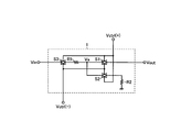
- FIG. 1 is a diagram illustrating a first embodiment of an analog switch circuit.
- the analog switch circuit 1 according to the first embodiment includes resistors R1 and R2 and CMOS type analog switches S1 and S2.
- the 1st end of analog switch S1 is connected to the application end of input voltage Vin via resistance R1.
- the second end of the analog switch S1 is connected to the application end of the output voltage Vout.
- the control end of the analog switch S1 is connected to the application end of the control voltage Vctrl (+).
- the inversion control terminal of the analog switch S1 is connected to the application terminal of the inversion control voltage Vctrl ( ⁇ ).
- the first end of the analog switch S2 is connected to the first end of the analog switch S1.
- the second end of the analog switch S2 is connected to the application end of the ground voltage GND through the resistor R2.
- the control end of the analog switch S1 is connected to the application end of the inversion control voltage Vctrl ( ⁇ ).
- the inversion control terminal of the analog switch S1 is connected to the application terminal of the control voltage Vctrl (+).
- Analog switches S1 and S2 each have an N-channel MOS field effect transistor N and a P-channel MOS field effect transistor P connected in parallel, similar to the analog switch ASW in FIG. 9A, and are applied to the respective gates. Are turned on / off in opposite phases according to the control voltage Vctrl (+) and the inverted control voltage Vctrl ( ⁇ ).
- the control voltage Vctrl (+) is set to the high level (power supply voltage VDD), and the inversion control voltage Vctrl ( ⁇ ) is set to the low level (ground voltage GND).
- VDD power supply voltage
- Vctrl inversion control voltage
- the control voltage Vctrl (+) is set to a low level (ground voltage GND), and the inversion control voltage Vctrl ( ⁇ ) is set to a high level (power supply voltage VDD).
- VDD power supply voltage
- the analog switch S1 is turned off, and the application end of the input voltage Vin and the application end of the output voltage Vout are interrupted.
- the input voltage Vin is within the normal range (from the power supply voltage VDD to the ground voltage GND), and of course, for some reason, at least the transistor P (see FIG. 9A) than the power supply voltage VDD. ), Even when an input voltage Vin ( ⁇ VDD + Vth) that is higher by the on-threshold voltage Vth is applied, the node voltage Va can be prevented from exceeding (VDD + Vth), so that the transistor included in the analog switch S1 It becomes possible to prevent erroneous turn-on against P's intention. Even when the input voltage Vin ( ⁇ GND ⁇ Vth) lower than the ground voltage GND by at least the on-threshold voltage Vth of the transistor N (see FIG. 9A) is applied for some reason, the node voltage Va is ( (GND ⁇ Vth) or less, it is possible to prevent erroneous turn-on contrary to the intention of the transistor N included in the analog switch S1.
- the analog switch S1 can be reliably turned off regardless of the input voltage Vin applied. It is possible to reliably block between the application end and the application end of the output voltage Vout.
- FIG. 2 is a diagram showing a second embodiment of the analog switch circuit.
- the analog switch circuit 1 of the second embodiment has substantially the same configuration as that of the first embodiment described above, and is characterized in that it further includes an analog switch S3. Therefore, the same components as those in the first embodiment are denoted by the same reference numerals as those in FIG. 1, and redundant descriptions are omitted. In the following, the characteristic portions of the second embodiment are mainly described.
- the analog switch S3 is inserted between the resistor R1 and the application terminal of the input voltage Vin, and is turned on / off in the same phase as the analog switch S1. With such a configuration, when the input voltage Vin is within the normal range during the off period of the analog switch circuit 1, the analog switch S3 is turned off. By separating R2, it becomes possible to suppress the influence on the pre-stage circuit connected to the application terminal of the input voltage Vin. On the other hand, when the input voltage Vin not less than (VDD + Vth) or not more than (GND ⁇ Vth) is applied during the OFF period of the analog switch circuit 1, the analog switch S3 is turned on unintentionally, as described above.
- the node voltage Va can be made to be (VDD + Vth) or less or (GND ⁇ Vth) or more using the resistors R1 and R2, the analog switch S1 is surely turned off, the application terminal of the input voltage Vin and the output voltage It is possible to reliably cut off from the application end of Vout.
- FIG. 3 is a diagram showing a third embodiment of the analog switch circuit.
- the analog switch circuit 1 of the third embodiment has substantially the same configuration as that of the second embodiment described above, and is characterized in that it further includes a resistor R3. Therefore, the same components as those in the second embodiment are denoted by the same reference numerals as those in FIG. 2, and redundant descriptions are omitted. In the following, the characteristic portions of the third embodiment are mainly described.
- the resistor R3 is inserted between the analog switch S3 and the input terminal of the input voltage Vin. With such a configuration, the current flowing from the application terminal of the input voltage Vin to the application terminal of the output voltage Vout during the ON period of the analog switch circuit 1 by arbitrarily setting the resistance value of the resistor R3 (for example, 1 k ⁇ ). It is possible to arbitrarily adjust the amount and protect the internal elements.
- FIG. 4 is a diagram illustrating a configuration example of the motor driving device.
- the motor drive device 10 of this configuration example is a main body that performs drive control of a three-phase motor (three-phase brushless motor) 20, and includes a selector 11, a filter 12, a comparator 13, a controller 14, a driver 15, Have
- the selector 11 sequentially selects and outputs each phase drive voltage U / V / W of the three-phase motor 20 according to the switching signal SW (U / V / W). More specifically, the selector 11 selects and outputs the drive voltage U during the M period of the drive voltage U (the transition period from the L period to the H period or the H period to the L period), and outputs the M of the drive voltage V. The drive voltage V is selected and output during the period, and the drive voltage W is selected and output during the M period of the drive voltage W. That is, the selector 11 selects and outputs a counter electromotive voltage generated in each phase coil of the three-phase motor 20. Further, the selector 11 always selects and outputs the common voltage COM of the three-phase motor 20 in accordance with the switching signal SW (C).
- the filter 12 is inserted between the selector 11 and the comparator 13 and removes noise components from the common voltage COM of the three-phase motor 20 selected by the selector 11 and each phase drive voltage U / V / W.
- an RC filter using a resistor and a capacitor can be used as the filter 12 (see FIG. 8).
- the cutoff frequency of the filter 12 may be set to any value, but may be set to 15 kHz, for example.
- the comparator 13 compares and compares the common voltage COM of the three-phase motor 20 applied to the inverting input terminal ( ⁇ ) and the phase driving voltages U / V / W sequentially applied to the non-inverting input terminal (+).
- a signal a is generated.
- the comparison signal a is at a low level when the common voltage COM is higher than each phase drive voltage U / V / W, and is at a high level when it is low.
- the controller 14 internally generates a speed signal A having a frequency corresponding to the rotational speed of the three-phase motor 20 based on the comparison signal a, and performs feedback control of the rotational speed of the three-phase motor 20 based on the speed signal A.
- each phase drive control signal (UH / UL, VH / VL, WH / WL) is generated. More specifically, the controller 14 conversely reduces the rotational speed of the three-phase motor 20 when the frequency of the speed signal A is higher than the predetermined target frequency, and conversely, the frequency of the speed signal A is the predetermined target frequency.
- each phase drive control signal (UH / UL, VH / VL, WH / WL) is generated so as to increase the rotational speed of the three-phase motor 20.
- the controller 14 performs PWM [pulse width modulation] control of each phase drive control signal (UH / UL, VH / VL, WH / WL) when controlling the speed of the three-phase motor 20.
- the driver 15 includes a power transistor (not shown) that is half-bridge connected for each phase of the three-phase motor 20, and each phase drive control signal (UH / UL, VH / VL, Each phase drive voltage U / V / W is generated based on (WH / WL).
- FIG. 5 is a time chart showing an operation example of the motor drive device 10, and in order from the top, the drive voltage U, the drive voltage V, the drive voltage W, the switching signal SW (U), the switching signal SW (V), The switching signal SW (W), the switching signal SW (C), and the speed signal A are depicted.
- vertical hatching of each phase drive voltage U / V / W indicates that each phase drive voltage U / V / W is PWM controlled.
- the switching signal SW (U) is set to the high level (power supply voltage VDD) during the M period of the drive voltage U and is set to the low level (ground voltage GND) during the remaining period.
- the switching signal SW (V) is at a high level (power supply voltage VDD) during the M period of the drive voltage V, and is at a low level (ground voltage GND) during the remaining period.
- the switching signal SW (W) is at a high level (power supply voltage VDD) during the M period of the drive voltage W, and is at a low level (ground voltage GND) during the remaining period.
- the switching signal SW (C) is always at a high level (VDD).
- the selector 11 selects and outputs the driving voltage U during the H period of the switching signal SW (U), selects and outputs the driving voltage V during the H period of the switching signal SW (V), and switches the switching signal SW (W).
- the drive voltage W is selected and output during the H period.
- the selector 11 always selects and outputs the common voltage COM in accordance with the switching signal SW (C) that is always at a high level.
- the common voltage COM and each phase drive voltage U / V / W output from the selector 11 are input to the comparator 13 via the filter 12.
- the comparator 13 compares the common voltage COM with each phase drive voltage U / V / W to generate a comparison signal a.
- the controller 14 internally generates a speed signal A having a frequency corresponding to the rotational speed of the three-phase motor 20 based on the comparison signal a.
- the ideal waveform of the speed signal A rises from a low level to a high level when each phase drive voltage U / V / W exceeds the common voltage COM in the process of transition from the L period to the H period.
- the phase drive voltage U / V / W falls below the common voltage COM in the process of transition from the H period to the L period, a rectangular wave falls from the high level to the low level.
- the rising timing and falling timing of the speed signal A may deviate from the original timing, which hinders the output feedback control by the controller 14 (as a result, drive control of the three-phase motor 20). May occur. Below, such a subject is demonstrated concretely.
- FIG. 6 is a diagram illustrating a first configuration example of the selector 11 (a configuration that can cause the above-described problem).
- the selector 11 of the first configuration example includes analog switches S1 (C), S1 (U), S1 (V), and S1 (W).
- the analog switch S1 (C) is connected between the application terminal of the common voltage COM and the first input terminal of the filter 12 (and thus the inverting input terminal ( ⁇ ) of the comparator 13).
- the analog switches S1 (U), S1 (V), and S1 (W) are respectively connected to the application terminal of each phase drive voltage (U, V, W) and the second input terminal of the filter 12 (and thus the comparator 13 is not connected). And an inverting input terminal (+).
- Analog switches S1 (C), S1 (U), S1 (V), and S1 (W) are respectively N-channel MOS field effect transistors N and P-channel transistors connected in parallel, as in analog switch ASW in FIG. 9A.
- a switching signal SW (C), SW (U), SW (V), SW (W) (each corresponding to the control voltage Vctrl (+) described above, which has a MOS field effect transistor P and is applied to each gate. )
- the inversion switching signals SWB (C), SWB (U), SWB (V), SWB (W) (each corresponding to the inversion control voltage Vctrl ( ⁇ ) described above).
- the analog switch S1 (C) is always turned on, and only one of the analog switches S1 (U), S1 (V), and S1 (W) is sequentially turned on.
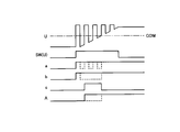
- FIG. 7A and 7B are time charts showing a first example (normal) and a second example (abnormal) of the output feedback operation, respectively, in order from the top: drive voltage U, switching signal SW (U), A comparison signal a, a filtered comparison signal b, a mask signal c, and a speed signal A are shown.
- drive voltage U switching signal SW (U)
- a comparison signal a a comparison signal a
- filtered comparison signal b a filtered comparison signal b
- a mask signal c a speed signal A
- the first example (normal time) of the output feedback operation will be described with reference to FIGS. 6 and 7A.
- the switching signal SW (U) is set to the high level
- the analog switch S1 (U) is turned on
- the switching signals SW (V) and SW (W) are set to the low level to switch the analog switch.
- S1 (V) and S1 (W) are turned off. Therefore, the selector 11 selectively outputs the drive voltage U, and the comparator 13 compares the drive voltage U with the common voltage COM to generate the comparison signal a.
- the comparison signal a is input from the comparator 13
- a predetermined filter process is performed on the comparison signal a.
- the filtered comparison signal b has a waveform in which unnecessary pulses due to the PWM component of the drive voltage U are partially removed compared to the original comparison signal a.
- the comparison signal b is detected (logic level determination) over a predetermined signal detection period (high level period of the mask signal c), and the logic level of the speed signal A is determined according to the detection result. Is switched.
- the ideal waveform of the speed signal A generated by the internal signal processing of the controller 14 is from a low level to a high level when the drive voltage U exceeds the common voltage COM in the process of transition from the L period to the H period. It becomes a square wave that rises to.
- the drive voltage of the phase that is PWM-driven may greatly swing to a voltage value higher than the power supply voltage VDD.
- VDD + Vth the voltage value exceeds (VDD + Vth)
- Vth the voltage value exceeds (VDD + Vth)
- the average value of the drive voltage (U + V) or (U + W) becomes higher than the common voltage COM, so that the comparison signal a generated by the comparator 13 or the controller 14 generates the average value.
- the comparison signal b after the filtering process is maintained at a substantially high level.
- the logical level of the speed signal A is switched at the same time as the predetermined signal detection period starts, so that the rising timing of the speed signal A deviates from the original timing, and output feedback control by the controller 14 (As a result, the drive control of the three-phase motor 20) may be hindered.
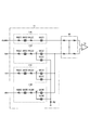
- FIG. 8 is a diagram illustrating a second configuration example of the selector 11 (a configuration that can solve the above-described problem).
- the selector 11 of the second configuration example includes analog switch circuits 11C, 11U, 11V, and 11W.
- the analog switch circuit 11C is connected between the application terminal of the common voltage COM and the first input terminal of the filter 12 (and thus the inverting input terminal ( ⁇ ) of the comparator 13).
- the analog switch circuits 11U, 11V, and 11W respectively have an application terminal for each phase drive voltage (U, V, W) and a second input terminal of the filter 12 (and a non-inverting input terminal (+) of the comparator 13). Connected between.
- the analog switch circuits 11U, 11V, and 11W basically have the same configuration as that of the analog switch circuit 1 in FIG. However, the analog switch circuits 11U, 11V, and 11W are not configured to have a resistor R2 for each phase, but are configured to share a single resistor R2 for all phases. With such a configuration, the circuit scale of the selector 11 can be reduced. Of course, a configuration having a resistor R2 for each phase may be employed.
- the analog switch circuit 11C has the same configuration as the analog switch circuits 11U, 11V, and 11W except that the analog switch S2 and the resistor R2 are removed in view of being always on. In this way, the dummy analog switch circuit 11C that is always on is provided between the application terminal of the common voltage COM and the first input terminal of the filter 12 (and thus the inverting input terminal ( ⁇ ) of the comparator 13).
- the signal loss between the common voltage COM and each phase drive voltage U / V / W in the selector 11 can be combined, so that the accuracy of the output feedback control by the controller 14 can be improved. It becomes possible.
- control voltages Vctrl (+) and Vctrl ( ⁇ ) depicted in FIG. 3 are omitted, but in any of the analog switch circuits 11C, 11U, 11V, and 11W, Similarly to FIG. 3, it is assumed that the switching signal SW corresponding to the control voltage Vctrl (+) and the inversion switching signal SWB corresponding to the inversion control voltage Vctrl ( ⁇ ) are applied. That is, the analog switches S1 and S2 are turned on / off in opposite phases, and the analog switches S1 and S3 are turned on / off in phase.
- the analog switch circuit 11U when the drive voltage U is selected and output, the analog switch circuit 11U is turned on and the analog switch circuits 11V and 11W are turned off.
- the analog switch circuit 11U that is turned on the analog switches S1 (U) and S3 (U) are turned on, and the application terminal of the drive voltage U and the second input terminal of the filter 12 (and thus the non-inverting input of the comparator 13).
- the end (+) is electrically connected.
- the analog switch S2 (U) since the analog switch S2 (U) is turned off, the node voltage U ′ applied to the first end of the analog switch S1 (U) is not unnecessarily lowered, and the normal signal path is adversely affected. There is nothing.
- the analog switch circuit 11V that is turned off, the analog switches S1 (V) and S3 (V) are turned off, and the analog switch S2 (V) is turned on.
- the analog switch S3 (V) is turned on unintentionally, but as described above, the resistance Since the node voltage V ′ can be set to (VDD + Vth) or less or (GND ⁇ Vth) or more using R1 and R2, the analog switch S1 (V) is surely turned off, and the application terminal of the drive voltage V and the filter Thus, it is possible to reliably block the connection between the second input terminal 12 and the non-inverting input terminal (+) of the comparator 13.
- the analog switch circuit 11W that is turned off is the same as described above.
- the configuration of the analog switch circuits 11C, 11U, 11V, and 11W is not limited to the configuration shown in FIG. 3, and the configurations shown in FIGS. 1 and 2 may be employed.
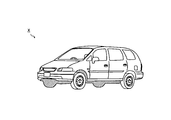
- the motor drive device 10 described above may be mounted on an electric vehicle X such as an electric vehicle or a hybrid vehicle (see FIG. 9), a home appliance Y such as an air conditioner (see FIG. 10), an industrial device, or the like. Is possible.
- the present invention can be suitably used, for example, as a technique for preventing malfunction during output feedback control in a motor drive device that performs drive control of a three-phase motor.
Landscapes
- Engineering & Computer Science (AREA)
- Power Engineering (AREA)
- Inverter Devices (AREA)
- Electronic Switches (AREA)
- Control Of Ac Motors In General (AREA)
Abstract
Description
図1は、アナログスイッチ回路の第1実施形態を示す図である。第1実施形態のアナログスイッチ回路1は、抵抗R1及びR2と、CMOS型のアナログスイッチS1及びS2と、を有する。
図4はモータ駆動装置の一構成例を示す図である。本構成例のモータ駆動装置10は、三相モータ(三相ブラシレスモータ)20の駆動制御を行う主体であって、セレクタ11と、フィルタ12と、コンパレータ13と、コントローラ14と、ドライバ15と、を有する。
以上で説明したモータ駆動装置10は、電気自動車やハイブリッド自動車などの電動車両X(図9を参照)、エアコンなどの家電機器Y(図10を参照)、或いは、産業機器などに搭載することが可能である。
なお、本明細書中に開示されている種々の技術的特徴は、上記実施形態のほか、その技術的創作の主旨を逸脱しない範囲で種々の変更を加えることが可能である。すなわち、上記実施形態は全ての点で例示であって、制限的なものではないと考えられるべきであり、本発明の技術的範囲は、上記実施形態の説明ではなく、特許請求の範囲によって示されるものであり、特許請求の範囲と均等の意味及び範囲内に属する全ての変更が含まれると理解されるべきである。
10 モータ駆動装置
11 セレクタ
11U、11V、11W、11C アナログスイッチ回路
12 フィルタ
13 コンパレータ
14 コントローラ
15 ドライバ
20 三相モータ(三相ブラシレスモータ)
S1、S2、S3 アナログスイッチ
R1、R2、R3 抵抗
X 電動車両
Y 家電機器
Claims (12)
- 第1抵抗と;
第2抵抗と;
第1端が前記第1抵抗を介して入力端に接続され、第2端が出力端に接続されたCMOS型の第1アナログスイッチと;
第1端が前記第1アナログスイッチの第1端に接続され、第2端が前記第2抵抗を介して接地端に接続され、前記第1アナログスイッチと逆相でオン/オフされるCMOS型の第2アナログスイッチと;
を有することを特徴とするアナログスイッチ回路。 - 前記第1抵抗と前記入力端との間に挿入され、前記第1アナログスイッチと同相でオン/オフされるCMOS型の第3アナログスイッチをさらに有することを特徴とする請求項1に記載のアナログスイッチ回路。
- 前記第3アナログスイッチと前記入力端との間に挿入された第3抵抗をさらに有することを特徴とする請求項2に記載のアナログスイッチ回路。
- 前記第1抵抗の抵抗値は、前記第2抵抗の抵抗値よりも大きい値に設定されていることを特徴とする請求項1~請求項3のいずれか一項に記載のアナログスイッチ回路。
- 三相モータの各相駆動電圧を順次選択して出力するセレクタと、
前記三相モータのコモン電圧と各相駆動電圧とを比較して比較信号を生成するコンパレータと、
前記比較信号に応じて前記三相モータの各相駆動制御信号を生成するコントローラと、
前記各相駆動制御信号に応じて前記三相モータの各相駆動電圧を生成するドライバと、
を有し、
前記セレクタは、前記各相駆動電圧の印加端と前記コンパレータとの間を各々導通/遮断するための手段として、各相毎に請求項1~請求項4のいずれか一項に記載のアナログスイッチ回路を含むことを特徴とするモータ駆動装置。 - 各相毎のアナログスイッチ回路は、前記第2抵抗を共有することを特徴とする請求項5に記載のモータ駆動装置。
- 前記セレクタは、前記コモン電圧の印加端と前記コンパレータとの間に挿入され、常時オン状態とされるダミーのアナログスイッチ回路をさらに含むことを特徴とする請求項5または請求項6に記載のモータ駆動装置。
- 前記セレクタと前記コンパレータとの間に挿入されたフィルタをさらに有することを特徴とする請求項5~請求項7のいずれか一項に記載のモータ駆動装置。
- 前記フィルタは、抵抗とキャパシタを用いたRCフィルタであることを特徴とする請求項8に記載のモータ駆動装置。
- 請求項5~請求項9のいずれか一項に記載のモータ駆動装置を備えたことを特徴とする電動車両。
- 請求項5~請求項9のいずれか一項に記載のモータ駆動装置を備えたことを特徴とする家電機器。
- 請求項5~請求項9のいずれか一項に記載のモータ駆動装置を備えたことを特徴とする産業機器。
Priority Applications (3)
| Application Number | Priority Date | Filing Date | Title |
|---|---|---|---|
| US14/125,979 US9306556B2 (en) | 2011-06-16 | 2012-06-08 | Analog-switch circuit and motor drive apparatus using same |
| JP2013520524A JP5677572B2 (ja) | 2011-06-16 | 2012-06-08 | アナログスイッチ回路及びこれを用いたモータ駆動装置 |
| CN201280028032.1A CN103597746B (zh) | 2011-06-16 | 2012-06-08 | 模拟开关电路及使用它的电机驱动装置 |
Applications Claiming Priority (2)
| Application Number | Priority Date | Filing Date | Title |
|---|---|---|---|
| JP2011-134368 | 2011-06-16 | ||
| JP2011134368 | 2011-06-16 |
Publications (1)
| Publication Number | Publication Date |
|---|---|
| WO2012173049A1 true WO2012173049A1 (ja) | 2012-12-20 |
Family
ID=47357038
Family Applications (1)
| Application Number | Title | Priority Date | Filing Date |
|---|---|---|---|
| PCT/JP2012/064754 Ceased WO2012173049A1 (ja) | 2011-06-16 | 2012-06-08 | アナログスイッチ回路及びこれを用いたモータ駆動装置 |
Country Status (4)
| Country | Link |
|---|---|
| US (1) | US9306556B2 (ja) |
| JP (1) | JP5677572B2 (ja) |
| CN (1) | CN103597746B (ja) |
| WO (1) | WO2012173049A1 (ja) |
Families Citing this family (1)
| Publication number | Priority date | Publication date | Assignee | Title |
|---|---|---|---|---|
| JP6694443B2 (ja) * | 2015-06-02 | 2020-05-13 | イー インク コーポレイション | ディスプレイを駆動するための装置 |
Citations (3)
| Publication number | Priority date | Publication date | Assignee | Title |
|---|---|---|---|---|
| JPH01236731A (ja) * | 1988-03-16 | 1989-09-21 | Nec Corp | 相補型アナログスイッチ |
| JP2001028891A (ja) * | 1999-07-13 | 2001-01-30 | Rohm Co Ltd | モータ駆動装置 |
| JP2006115599A (ja) * | 2004-10-14 | 2006-04-27 | Renesas Technology Corp | モータの駆動制御装置および起動方法 |
Family Cites Families (4)
| Publication number | Priority date | Publication date | Assignee | Title |
|---|---|---|---|---|
| JP2600753B2 (ja) * | 1988-02-03 | 1997-04-16 | 日本電気株式会社 | 入力回路 |
| CN1166090A (zh) * | 1996-10-21 | 1997-11-26 | 成都希望电子研究所 | 一种代替可变电阻器的模拟开关电路 |
| JP2003189680A (ja) * | 2001-12-12 | 2003-07-04 | Matsushita Electric Ind Co Ltd | コイル負荷の駆動装置 |
| US20120221269A1 (en) * | 2011-02-28 | 2012-08-30 | Kent David Wanner | Method and system for determining dc bus leakage |
-
2012
- 2012-06-08 CN CN201280028032.1A patent/CN103597746B/zh active Active
- 2012-06-08 WO PCT/JP2012/064754 patent/WO2012173049A1/ja not_active Ceased
- 2012-06-08 JP JP2013520524A patent/JP5677572B2/ja active Active
- 2012-06-08 US US14/125,979 patent/US9306556B2/en active Active
Patent Citations (3)
| Publication number | Priority date | Publication date | Assignee | Title |
|---|---|---|---|---|
| JPH01236731A (ja) * | 1988-03-16 | 1989-09-21 | Nec Corp | 相補型アナログスイッチ |
| JP2001028891A (ja) * | 1999-07-13 | 2001-01-30 | Rohm Co Ltd | モータ駆動装置 |
| JP2006115599A (ja) * | 2004-10-14 | 2006-04-27 | Renesas Technology Corp | モータの駆動制御装置および起動方法 |
Also Published As
| Publication number | Publication date |
|---|---|
| US20140117914A1 (en) | 2014-05-01 |
| JPWO2012173049A1 (ja) | 2015-02-23 |
| JP5677572B2 (ja) | 2015-02-25 |
| US9306556B2 (en) | 2016-04-05 |
| CN103597746B (zh) | 2016-08-31 |
| CN103597746A (zh) | 2014-02-19 |
Similar Documents
| Publication | Publication Date | Title |
|---|---|---|
| JP4879645B2 (ja) | モータ駆動装置及びこれを用いた電気機器 | |
| JP5537272B2 (ja) | 負荷駆動回路装置及びこれを用いた電気機器 | |
| US8520346B2 (en) | Abnormality detection circuit, load driving device, and electrical apparatus | |
| US9906215B2 (en) | Load-driving circuit | |
| EP3046240B1 (en) | Integrated circuit charge pump with failure protection | |
| US8933714B2 (en) | Level shift circuit using parasitic resistor in semiconductor substrate | |
| WO2013137244A1 (ja) | インバータ装置及びパワーステアリング装置 | |
| JP6402832B2 (ja) | 半導体デバイス駆動回路およびインバータ装置 | |
| JP4531500B2 (ja) | 半導体装置および半導体装置モジュール | |
| TWI394361B (zh) | 馬達驅動電路 | |
| JP2013085419A (ja) | 電力変換装置 | |
| US20080186603A1 (en) | Vehicle mirror device | |
| JP6708003B2 (ja) | 給電制御装置 | |
| JP2011188271A (ja) | ゲート駆動回路 | |
| JP6254029B2 (ja) | 駆動制御装置及び故障検知方法 | |
| US8994437B2 (en) | Semiconductor device and circuit for controlling potential of gate of insulated gate type switching device | |
| JP6384300B2 (ja) | 電力変換回路の駆動装置 | |
| JP5677572B2 (ja) | アナログスイッチ回路及びこれを用いたモータ駆動装置 | |
| JP5060750B2 (ja) | モータ駆動回路およびそれを用いた電子機器 | |
| JP2018196115A (ja) | 電子モジュールおよび自動車ならびにモジュールのスイッチオン過程中の入力電流を制限する方法 | |
| JP6023551B2 (ja) | アナログスイッチ回路およびそれを備える電気機器 | |
| JP4886023B2 (ja) | スイッチング素子の駆動回路 | |
| WO2007004418A1 (ja) | 半導体集積回路装置 | |
| JP2006081363A (ja) | コイル負荷駆動回路及びそれを備えた光ディスク装置 | |
| JP4475257B2 (ja) | 電流制限回路 |
Legal Events
| Date | Code | Title | Description |
|---|---|---|---|
| 121 | Ep: the epo has been informed by wipo that ep was designated in this application |
Ref document number: 12799982 Country of ref document: EP Kind code of ref document: A1 |
|
| ENP | Entry into the national phase |
Ref document number: 2013520524 Country of ref document: JP Kind code of ref document: A |
|
| WWE | Wipo information: entry into national phase |
Ref document number: 14125979 Country of ref document: US |
|
| NENP | Non-entry into the national phase |
Ref country code: DE |
|
| 122 | Ep: pct application non-entry in european phase |
Ref document number: 12799982 Country of ref document: EP Kind code of ref document: A1 |