WO2012173044A1 - 積層体、液晶モジュール、積層体の製造方法及び液晶モジュールの製造方法 - Google Patents
積層体、液晶モジュール、積層体の製造方法及び液晶モジュールの製造方法 Download PDFInfo
- Publication number
- WO2012173044A1 WO2012173044A1 PCT/JP2012/064724 JP2012064724W WO2012173044A1 WO 2012173044 A1 WO2012173044 A1 WO 2012173044A1 JP 2012064724 W JP2012064724 W JP 2012064724W WO 2012173044 A1 WO2012173044 A1 WO 2012173044A1
- Authority
- WO
- WIPO (PCT)
- Prior art keywords
- liquid crystal
- backlight
- photosensitive sheet
- crystal module
- light
- Prior art date
- Legal status (The legal status is an assumption and is not a legal conclusion. Google has not performed a legal analysis and makes no representation as to the accuracy of the status listed.)
- Ceased
Links
Images


Classifications
-
- G—PHYSICS
- G02—OPTICS
- G02F—OPTICAL DEVICES OR ARRANGEMENTS FOR THE CONTROL OF LIGHT BY MODIFICATION OF THE OPTICAL PROPERTIES OF THE MEDIA OF THE ELEMENTS INVOLVED THEREIN; NON-LINEAR OPTICS; FREQUENCY-CHANGING OF LIGHT; OPTICAL LOGIC ELEMENTS; OPTICAL ANALOGUE/DIGITAL CONVERTERS
- G02F1/00—Devices or arrangements for the control of the intensity, colour, phase, polarisation or direction of light arriving from an independent light source, e.g. switching, gating or modulating; Non-linear optics
- G02F1/01—Devices or arrangements for the control of the intensity, colour, phase, polarisation or direction of light arriving from an independent light source, e.g. switching, gating or modulating; Non-linear optics for the control of the intensity, phase, polarisation or colour
- G02F1/13—Devices or arrangements for the control of the intensity, colour, phase, polarisation or direction of light arriving from an independent light source, e.g. switching, gating or modulating; Non-linear optics for the control of the intensity, phase, polarisation or colour based on liquid crystals, e.g. single liquid crystal display cells
- G02F1/133—Constructional arrangements; Operation of liquid crystal cells; Circuit arrangements
- G02F1/1333—Constructional arrangements; Manufacturing methods
- G02F1/1335—Structural association of cells with optical devices, e.g. polarisers or reflectors
- G02F1/1336—Illuminating devices
- G02F1/133602—Direct backlight
- G02F1/133611—Direct backlight including means for improving the brightness uniformity
-
- G—PHYSICS
- G02—OPTICS
- G02F—OPTICAL DEVICES OR ARRANGEMENTS FOR THE CONTROL OF LIGHT BY MODIFICATION OF THE OPTICAL PROPERTIES OF THE MEDIA OF THE ELEMENTS INVOLVED THEREIN; NON-LINEAR OPTICS; FREQUENCY-CHANGING OF LIGHT; OPTICAL LOGIC ELEMENTS; OPTICAL ANALOGUE/DIGITAL CONVERTERS
- G02F1/00—Devices or arrangements for the control of the intensity, colour, phase, polarisation or direction of light arriving from an independent light source, e.g. switching, gating or modulating; Non-linear optics
- G02F1/01—Devices or arrangements for the control of the intensity, colour, phase, polarisation or direction of light arriving from an independent light source, e.g. switching, gating or modulating; Non-linear optics for the control of the intensity, phase, polarisation or colour
- G02F1/13—Devices or arrangements for the control of the intensity, colour, phase, polarisation or direction of light arriving from an independent light source, e.g. switching, gating or modulating; Non-linear optics for the control of the intensity, phase, polarisation or colour based on liquid crystals, e.g. single liquid crystal display cells
- G02F1/133—Constructional arrangements; Operation of liquid crystal cells; Circuit arrangements
- G02F1/1333—Constructional arrangements; Manufacturing methods
- G02F1/1335—Structural association of cells with optical devices, e.g. polarisers or reflectors
- G02F1/1336—Illuminating devices
- G02F1/133602—Direct backlight
- G02F1/133606—Direct backlight including a specially adapted diffusing, scattering or light controlling members
Definitions
- Patent Document 1 prints with a print pattern in which the dot area ratio increases as the amount of light reaching from the light source increases, thereby reducing the light transmission amount, A brightness distribution uniformizing sheet and a backlight unit aimed at preventing the occurrence of streaky brightness unevenness are described.
- Japanese Patent Publication Japanese Patent Laid-Open No. 2010-49824 (Publication Date: March 4, 2010)”
- the display unevenness of the backlight can be improved by laminating the light and dark photosensitive sheet on the backlight for the liquid crystal module.
- the liquid crystal module according to the present invention is formed by stacking the laminate according to the present invention and a liquid crystal panel, and the liquid crystal panel and the backlight are stacked with the photosensitive sheet interposed therebetween. It is characterized by that.
- the method for producing a laminate according to the present invention includes a step of exposing a photosensitive sheet with light emitted from a backlight for a liquid crystal module, developing the exposed photosensitive sheet, and the back And the step of laminating the photosensitive sheet after development on the light, so that it is possible to provide a laminate in which the display unevenness of the backlight is suppressed even when the shape of the display unevenness is not fixed. .
- the method for producing a liquid crystal module according to the present invention includes a step of exposing and developing a photosensitive sheet with light emitted from a laminate of a liquid crystal panel and a backlight for the liquid crystal module as described above. Removing the liquid crystal panel and the backlight after exposing the photosensitive sheet, and sandwiching the developed photosensitive sheet between the liquid crystal panel and the backlight, the liquid crystal panel, And a step of laminating the backlight and the photosensitive sheet. Therefore, it is possible to provide a liquid crystal module that can suppress the display unevenness of the backlight and the liquid crystal panel even when the shape of the display unevenness is not fixed. .
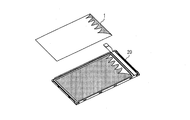
- FIG. 3 is a diagram for explaining a configuration of a photosensitive sheet 1 provided in a laminated body 10.
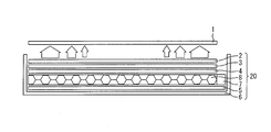
- FIG. 2 is a schematic diagram showing a state in which the photosensitive sheet 1 is exposed using light from a backlight 20. It is a figure which shows typically the structure of the liquid crystal module 30 which concerns on Embodiment 2.
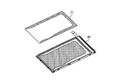
- FIG. 4 is a diagram for explaining a configuration of a photosensitive sheet 31 provided in the liquid crystal module 30.
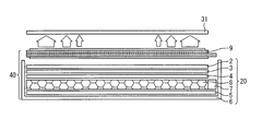
- FIG. FIG. 4 is a schematic diagram showing a state where exposure of a photosensitive sheet 31 is performed using light of a temporarily manufactured liquid crystal module 40.
- the laminate 10 includes a photosensitive sheet 1, lens sheets 2 and 3, a lower diffusion sheet 4, a reflection sheet 5, a frame 6, an LED 7, and a light guide plate 8.
- the backlight 20 shown in FIG. 2 includes a lens sheet 2, a lens sheet 3, a lower diffusion sheet 4, a reflection sheet 5, a frame 6, an LED 7, and a light guide plate 8.
- the brightness difference is reflected on the photosensitive sheet 1 by performing exposure using the light emission of the backlight 20. That is, since the unevenness is eliminated by arranging the dark portion pattern with respect to the bright portion, it is possible to cope with a difference in the shape of the unevenness in each backlight.
- the specific material of the photosensitive sheet 1 may be set as appropriate according to the purpose of the liquid crystal module to be manufactured, and examples thereof include polyester. Polyesters are excellent in optical properties and excellent in mechanical strength, dimensional stability, heat resistance, and chemical resistance. Specific products include 100TMAX (product name), 125PX (product name) (manufactured by Kodak), Neopan 100A (product name) CROS (product name), Neopan SS (product name) (manufactured by FUJIFILM), PAN100 (Product Name) (Konica Minolta), AgfapanAPX100 (Product Name) (Agfa), PAN F Plus (Product Name), DELTA100 (Product Name), Pan100 (Product Name), FP4 Plus (Product Name), fomapan100 (Product name) (manufactured by Foma), efkeKB25 (product name), efkeKB50 (product name), efkeKB100 (product name) (manufactured by Photochemica),
- the thickness of the photosensitive sheet 1 is preferably 0.03 to 0.2 mm, for example, in consideration of the characteristics of the thin liquid crystal module, the light transmittance, and the like.
- the conditions other than the material and thickness may be set as appropriate according to exposure conditions such as light transmittance before exposure, exposure time, and workplace environment.
- the upper diffusion sheet is a transparent base provided with a layer for diffusing light with beads or the like, and the entire surface has the same transmittance and diffuses light in the same manner over the entire surface.
- this causes a problem that the overall luminance is lowered.
- a photosensitive sheet is used as in one embodiment of the present invention, only the high-luminance portion is darkened to achieve uniformity of the entire surface. Therefore, there is an advantage that a decrease in luminance can be suppressed as compared to inserting a diffusion sheet that decreases the luminance of the entire screen.
- the laminate according to one embodiment of the present invention uses a photosensitive sheet as an alternative to the upper diffusion sheet, the display unevenness of the backlight is reduced without changing the number of conventional components and reducing the brightness of the entire screen. It also has the advantage of being able to cope.
- the lower diffusion sheet 4 is for uniformly spreading the light emitted from the light guide plate 8 and sending it to the lens sheet 3.
- the lower diffusion sheet 4 is laminated on the light guide plate 8 and below the lens sheet 3.
- the reflection plate 5 is for reflecting light emitted downward from the light guide plate 8 upward.
- the reflection plate 5 is laminated below the light guide plate 8 and is laid on the bottom of the frame 6.
- the frame 6 is a housing for housing the photosensitive sheet 1, the lens sheets 2 and 3, the lower diffusion sheet 4, the reflection sheet 5, the LED 7, and the light guide plate 8.
- LED 7 is a linear light source in the laminate 10.
- the LED 7 emits light to the end of the light guide plate 8.
- point light sources may be used side by side.
- the light guide plate 8 receives light emitted from the LED 7 at the end of the side surface, guides it to the surface, and emits light upward from the surface. Thereby, the light-guide plate 8 can be used as an upward surface light source.
- FIG. 3 is a schematic diagram showing a state in which the photosensitive sheet 1 is exposed using the light of the backlight 20.
- the reflection sheet 5 and the light guide plate 8 are assembled in the frame 6 with the reflection sheet 5 facing down.
- the LED 7 is mounted so that light can be applied to the side surface of the light guide plate 8.
- the lower diffusion sheet 4 and the lens sheets 2 and 3 are assembled in the frame 6. Specifically, the lower diffusion sheet 4, the lens sheet 3, and the lens sheet 2 are sequentially laminated in the order above the light guide plate 8. Thereby, the backlight 20 is obtained.
- the laminated body 10 completed by incorporating the photosensitive sheet 1 into the backlight 20 can improve display unevenness of the backlight 20.
- the thickness of the arrow in FIG. 3 represents the intensity of light from the backlight 20.
- the photosensitive sheet 1 By exposing the photosensitive sheet 1 with the light of the backlight 20, light and dark according to the intensity of light can be reflected on the photosensitive sheet 1. In other words, where the light is strong, the color is dark, and where the light is weak, the color is light. Thereafter, the photosensitive sheet 1 having light and darkness can be produced by developing.
- the developed photosensitive sheet 1 is laminated on the backlight 20.
- the photosensitive sheet 1 is laminated on the backlight 20 in the same direction as when exposed by the backlight 20.
- the laminated body 10 is obtained.
- the display unevenness may be appropriately suppressed, or the backlight 20 may emit light for inspection.
- FIG. 4 is a diagram schematically showing the structure of the liquid crystal module 30 according to the present embodiment.
- FIG. 5 is a diagram for explaining the configuration of the photosensitive sheet 31 provided in the liquid crystal module 30.
- the liquid crystal module 30 includes a photosensitive sheet 31, lens sheets 2 and 3, a lower diffusion sheet 4, a reflection sheet 5, a frame 6, an LED 7, a light guide plate 8, and a liquid crystal panel 9.
- FIG. 5 shows a temporarily manufactured liquid crystal module 40 (a liquid crystal panel and a backlight for a liquid crystal module laminated) 40, which is obtained by removing the photosensitive sheet 31 from the liquid crystal module 30.
- the provisional liquid crystal module 40 includes lens sheets 2 and 3, a lower diffusion sheet 4, a reflection sheet 5, a frame 6, an LED 7, a light guide plate 8, and a liquid crystal panel 9, which are the backlight of the liquid crystal panel 9 and the first embodiment. It can be said that 20 is laminated.
- photosensitive sheet 31 is sandwiched between the lens sheet 2 and the liquid crystal panel 9.
- the color of the temporary liquid crystal module 40 in the photosensitive sheet 31 that is strongly exposed to light is dark and the light that is weakly exposed to light is light. Therefore, when the photosensitive sheet 31 is laminated on the temporarily produced liquid crystal module 40, the light / dark difference can be canceled. Therefore, display unevenness is improved in the liquid crystal module 30 that is completed by incorporating the photosensitive sheet 31 into the temporarily manufactured liquid crystal module 40.
- the thickness of the arrow in FIG. 6 represents the intensity of light from the temporarily manufactured liquid crystal module 40.
- the photosensitive sheet is made of polyester, a photosensitive sheet having excellent optical properties, mechanical strength, dimensional stability, heat resistance, and chemical resistance can be obtained.
- the photosensitive sheet may be developed after being exposed to light emitted from a laminate of the liquid crystal panel and the backlight. preferable.
Landscapes
- Physics & Mathematics (AREA)
- Nonlinear Science (AREA)
- Mathematical Physics (AREA)
- Chemical & Material Sciences (AREA)
- Crystallography & Structural Chemistry (AREA)
- General Physics & Mathematics (AREA)
- Optics & Photonics (AREA)
- Planar Illumination Modules (AREA)
- Liquid Crystal (AREA)
Abstract
本発明の一実施形態に係る積層体(10)は、液晶モジュール用のバックライト(20)と、感光シート(1)と、が積層されてなり、感光シート(1)は、バックライト(20)から発光される光で露光された後に、現像したものである。
Description
本発明はバックライトを含む積層体、液晶モジュール、積層体の製造方法及び液晶モジュールの製造方法に関するものである。
バックライトユニットの輝度ムラを防止する技術として、特許文献1には、光源から到達する光量が多くなるに従って網点面積率が高くなる印刷パターンで印刷して、光線透過量を低減させることにより、筋状の輝度ムラの発生を防止することを目的としている輝度分布均一化シート及びバックライトユニットが記載されている。
液晶モジュールの表示ムラ及びバックライト自身の表示ムラは、液晶モジュールを開発する場合、頻繁に問題となる。表示ムラの原因は、液晶パネルによる場合とバックライトによる場合の2種類に分類できる。液晶パネルの場合は、注入口ムラ、周辺ムラ及び液晶のセル厚が原因となることが多い。バックライトの場合は、LED近傍のムラ、シートのたわみムラ等の構造、材料が原因となることが多い。
特許文献1に記載の技術では、バックライトの線状光源の明暗をスクリーニングパターンで暗くし、明暗差をなくすものであるため、光源の形があらかじめわかっているものでなければならない。さらに、決まったムラパターンにしか対応できず、微調整ができないという問題がある。
本発明は、このような事情に鑑みて成されたものであり、表示ムラの形状が定まっていない場合でも表示ムラを抑制できる、バックライトを含む積層体及び液晶モジュールを提供することを課題とする。
上記の課題を解決するために、本発明に係る積層体は、液晶モジュール用のバックライトと、感光シートと、が積層されてなり、上記感光シートは、当該バックライトから発光される光で露光された後に、現像したものであることを特徴としている。
上記の構成によれば、積層体を製造する際に、感光シートを露光し、それを現像することでバックライトの明暗差を打ち消す明暗を有する感光シートができる。
その明暗を有する感光シートを液晶モジュール用バックライトに積層することで、バックライトの表示ムラを改善することができる。
よって、表示ムラの形状が定まっていない場合でも、バックライトの表示ムラを抑制した積層体を提供することができる。
また、本発明に係る液晶モジュールは、上記の本発明に係る積層体と、液晶パネルと、が積層してなり、上記感光シートを挟んで、上記液晶パネルと上記バックライトとが積層していることを特徴とする。
上記の構成によれば、積層体を製造する際に、感光シートを露光し、それを現像することでバックライトの明暗差を打ち消す明暗を有する感光シートができる。その感光シートを液晶パネルとバックライトとの間に挟んで積層する。これにより、表示ムラの形状が定まっていない場合でも、バックライトの表示ムラを抑制した液晶モジュールを提供することができる。
また、本発明に係る積層体の製造方法は、液晶モジュール用のバックライトから発光される光で感光シートを露光して、露光した当該感光シートを現像する工程と、当該バックライト上に現像後の当該感光シートを積層する工程と、を含むことを特徴としている。
上記の構成によれば、積層体を製造する際に、感光シートを露光し、それを現像することでバックライトの明暗差を打ち消す明暗を有する感光シートができる。
その明暗を有する感光シートを液晶モジュール用バックライトに積層することで、バックライトの表示ムラを改善することができる。
よって、表示ムラの形状が定まっていない場合でも、バックライトの表示ムラを抑制した積層体を提供することができる。
また、本発明に係る液晶モジュールの製造方法は、液晶パネルと液晶モジュール用のバックライトとを積層させたものから発光される光で、感光シートを露光して現像する工程と、上記感光シートを露光した後に、上記液晶パネルと上記バックライトとを外す工程と、当該液晶パネルと当該バックライトとの間に、現像した後の上記感光シートを挟んで、当該液晶パネル、当該バックライト及び当該感光シートを積層する工程と、を含むことを特徴としている。
上記の構成によれば、液晶モジュールを製造する際に、感光シートを露光し、それを現像することでバックライト及び液晶パネルの明暗差を打ち消す明暗を有する感光シートができる。その感光シートを液晶パネルとバックライトとの間に挟んで積層する。これにより、表示ムラの形状が定まっていない場合でも、バックライト及び液晶パネルの表示ムラを抑制した液晶モジュールを提供することができる。
本発明の他の目的、特徴、および優れた点は、以下に示す記載によって十分分かるであろう。また、本発明の利点は、添付図面を参照した次の説明で明白になるであろう。
以上のように、本発明に係る積層体は、液晶モジュール用のバックライトと、感光シートと、が積層されてなり、上記感光シートは、当該バックライトから発光される光で露光された後に、現像したものであるので、表示ムラの形状が定まっていない場合でも、バックライトの表示ムラを抑制した積層体を提供することができるという効果を奏する。
また、本発明に係る液晶モジュールは、以上のように、上記感光シートが、上記液晶パネルと上記バックライトとを積層させたものから発光される光で露光された後に、現像したものであるので、表示ムラの形状が定まっていない場合でも、バックライト及び液晶パネルの表示ムラを抑制した液晶モジュールを提供することができるという効果を奏する。
また、本発明に係る積層体の製造方法は、以上のように、液晶モジュール用のバックライトから発光される光で感光シートを露光して、露光した当該感光シートを現像する工程と、当該バックライト上に現像後の当該感光シートを積層する工程と、を含むので、表示ムラの形状が定まっていない場合でも、バックライトの表示ムラを抑制した積層体を提供することができるという効果を奏する。
また、本発明に係る液晶モジュールの製造方法は、以上のように、液晶パネルと液晶モジュール用のバックライトとを積層させたものから発光される光で、感光シートを露光して現像する工程と、上記感光シートを露光した後に、上記液晶パネルと上記バックライトとを外す工程と、当該液晶パネルと当該バックライトとの間に、現像した後の上記感光シートを挟んで、当該液晶パネル、当該バックライト及び当該感光シートを積層する工程と、を含むので、表示ムラの形状が定まっていない場合でも、バックライト及び液晶パネルの表示ムラを抑制した液晶モジュールを提供することができるという効果を奏する。
以下、本発明の実施の形態について、詳細に説明する。
<実施形態1>
〔積層体10〕
本発明に係る積層体の一実施形態について図1~図2に基づいて説明すると以下のとおりである。図1は本実施形態に係る積層体10の構造を模式的に示す図である。図2は積層体10が備える感光シート1の構成を説明するための図である。
〔積層体10〕
本発明に係る積層体の一実施形態について図1~図2に基づいて説明すると以下のとおりである。図1は本実施形態に係る積層体10の構造を模式的に示す図である。図2は積層体10が備える感光シート1の構成を説明するための図である。
図1に示すように積層体10は、感光シート1、レンズシート2及び3、下拡散シート4、反射シート5、フレーム6、LED7、導光板8を備えている。図2に示すバックライト20はレンズシート2、レンズシート3、下拡散シート4、反射シート5、フレーム6、LED7、導光板8により構成される。
感光シート1は、バックライト20の表示ムラを抑制する構成を有している。具体的には、図2に示すように、バックライト20には明暗の表示ムラがあるが、バックライト20において明るい部分に対応する位置は暗く、暗い部分に対応する位置は明るくなるように、感光シート1に色の濃淡のムラが形成されている。つまり、バックライト20から発光される光の明暗の差を少なくするように、色の濃淡がついている。この色の濃淡は、換言すれば、感光シートを構成する粒子の密度の高低である。感光シートの色が濃ければ、粒子の密度が高く、光を通し難い。感光シートの色が淡ければ、粒子の密度が低く、光を通しやすい。
本実施形態では、このように、バックライト20から発光される光の明暗の差を少なくするように、感光シート1に色の濃淡をつけることでバックライト20の表示ムラを抑制する。このような感光シート1の色の濃淡は、予めバックライト20で発する光で感光シート1を露光して、現像することで形成される。このようにすれば、バックライト20の表示ムラに応じて、当該表示ムラを抑制するための濃淡を感光シート1につけることができる。従って、表示ムラの形状が定まっていない場合でも、バックライト20の表示ムラを抑制した、液晶モジュールのためのバックライト20を含む積層体10を得ることができる。本発明の一実施形態においては、後述のように、バックライトのみならず、液晶パネルをも組み合わせて露光すれば、液晶モジュール全体の表示ムラにも対応させることができる。換言すれば、本実施形態では、バックライト20の発光を利用し露光することで、輝度差を感光シート1に反映させている。つまり、明部に対して、暗部のパターンを配することによりムラを無くしているので、個々のバックライトでムラの形状に違いがあっても対応可能である。
感光シート1の具体的な材質としては、製造する液晶モジュールの目的等に応じて適宜設定すればよいが、例えば、ポリエステル等が挙げられる。ポリエステルは、光学特性に優れ、機械的強度、寸法安定性、耐熱性、耐薬品性にも優れている。具体的な商品としては、100TMAX(商品名)、125PX(商品名)(コダック社製)、ネオパン100A(商品名)CROS(商品名)、ネオパンSS(商品名)(富士フイルム社製)、PAN100(商品名)(コニカミノルタ社製)、AgfapanAPX100(商品名)(アグファ社製)、PAN Fプラス(商品名)、DELTA100(商品名)、Pan100(商品名)、FP4プラス(商品名)、fomapan100(商品名)(フォマ社製)、efkeKB25(商品名)、efkeKB50(商品名)、efkeKB100(商品名)(フォトケミカ社製)、RolleiPAN25(商品名)、RolleiORTHO25(商品名)、Rollei Advanced TechnicalPan1.1(商品名)、RolleiRETRO80S(商品名)、RolleiRetro100(商品名)(マコ社製)等が挙げられる。
また、感光シート1の厚さとしては、薄型を特徴とする液晶モジュールの特性、光の透過率等を考慮すると、例えば0.03~0.2mmであることが好ましい。
材質、厚さ以外の条件については、露光前の光透過率、露光時間、作業場の環境等の露光条件等に応じて適宜設定すればよい。
従来、上拡散シートを挿入することで、バックライト及び液晶パネルのムラを見えにくくすることはしばしば行われている。具体的には、上拡散シートは透明基材にビーズ等で光を拡散させる層を設けたものであり、面全体が同じ透過率で、面全体で同じように光を拡散させる。この上拡散シートを用いて、バックライトの周辺部の表示ムラを抑制する技術もある。しかし、これでは全体の輝度が低下するという問題が生じる。一方、本発明の一実施形態ように感光シートを用いれば、高輝度の部分だけを暗くすることにより、面全体の均一性を図っている。そのため、画面全体の輝度を低下させる拡散シートを挿入するよりも輝度の低下を抑制することができるという利点がある。
また、本発明の一実施形態に係る積層体は、上拡散シートの代替として感光シートを用いるため、従来の部品点数を変化させること及び画面全体の輝度を低下させることなくバックライトの表示ムラに対応できるという利点をも有している。
なお、感光シート1は、レンズシート2の上に積層している。
レンズシート2及び3は、導光板8から発せられ下拡散シート4にて広がった光を上方(図1において、導光板8からみて感光シート1のある方向を「上」とする)に集めるためのものである。レンズシート2及び3は下拡散シート4の上であって、感光シート1の下に積層している。
下拡散シート4は、導光板8から発せられた光を均一に広げて、レンズシート3に送るためのものである。下拡散シート4は導光板8の上であって、レンズシート3の下に積層している。
反射板5は、導光板8から下方に発せられた光を上方に反射するためのものである。反射板5は導光板8の下に積層してあり、フレーム6の底に敷かれている。
フレーム6は、感光シート1、レンズシート2及び3、下拡散シート4、反射シート5、LED7、導光板8を収めるための筐体である。
LED7は積層体10における線状光源である。LED7は導光板8の端部に対して光を発する。本実施形態では線状光源を用いる場合について説明するが、点光源を並べて用いるなどしてもよい。
導光板8は、LED7から発せられた光を側面の端部で受光して、その表面に導き、当該表面から上方に光を発するためのものである。これにより、導光板8を上方への面光源とすることができる。
〔積層体10の製造方法〕
次に図3に基づいて、本実施形態に係る積層体10の製造方法を説明する。図3はバックライト20の光を用いて、感光シート1の露光を行なっている様子示す模式図である。
次に図3に基づいて、本実施形態に係る積層体10の製造方法を説明する。図3はバックライト20の光を用いて、感光シート1の露光を行なっている様子示す模式図である。
まず、反射シート5及び導光板8をフレーム6内に、反射シート5が下になるようにして組込む。次に、LED7を導光板8の側面に光を当てることができるように取り付ける。
次に、下拡散シート4、レンズシート2及び3をフレーム6内に組込む。具体的には、導光板8からみて上方に、順に下拡散シート4、レンズシート3、レンズシート2の順になるように積層する。これによりバックライト20が得られる。
次に、バックライト20から発光される光で感光シート1を露光して、露光した当該感光シート1を現像する工程を行なう。
露光とは、フィルム、シート等に光源から光を照射し、光に応じた潜像を出現させる操作をいう。現像とは、目に見えない又は見えにくい潜像を定着させる操作をいう。これらの操作をすることにより、明暗を有する感光シート1が作成できる。
露光、現像させることにより、感光シート1の中でバックライト20の光が強く当たったところは色が濃く、光が弱く当たったところは色が薄くなる。そのため、感光シート1をバックライト20に積層させると明暗差が打ち消すことができる。よって、感光シート1をバックライト20に組込んで完成する積層体10はバックライト20の表示ムラを改善することができる。
なお、図3中の矢印の太さはバックライト20からの光の強弱を表している。バックライト20の光で感光シート1を露光することにより、光の強弱にあわせた明暗を感光シート1に反映させることができる。つまり光の強かったところは色の濃く、光の弱かったところは色が薄くなっている。その後現像することにより、明暗を有する感光シート1を作成することができる。
なお、感光シート1を露光する際の、バックライト20の発光の条件としては、例えば、製品として使用するときと同様の条件で発光させればよい。
次に、バックライト20上に現像後の感光シート1を積層する。このとき、感光シート1を、バックライト20で露光したときと同じ向きで、バックライト20上に積層する。これにより、積層体10が得られる。積層体10を得た後は、適宜、表示ムラが抑制されているか、バックライト20を発光させて検査を行なってもよい。
なお、得られた積層体10の上に感光シート1を挟んで、液晶パネルを積層する工程を行なうと液晶モジュールが得られる。これは、本発明に係る液晶モジュールの製造方法の一実施形態である。
<実施形態2>
〔液晶モジュール30〕
本発明に係る液晶モジュールの一実施形態について図4~図5に基づいて説明すれば、以下の通りである。なお、説明の便宜上、実施形態1に係る構成要素と同様の機能を有する構成要素には同一の番号を付し、その説明を省略する。本実施形態では、主に、実施形態1との相違点について説明するものとする。図4は本実施形態に係る液晶モジュール30の構造を模式的に示す図である。図5は液晶モジュール30が備える感光シート31の構成を説明するための図である。
〔液晶モジュール30〕
本発明に係る液晶モジュールの一実施形態について図4~図5に基づいて説明すれば、以下の通りである。なお、説明の便宜上、実施形態1に係る構成要素と同様の機能を有する構成要素には同一の番号を付し、その説明を省略する。本実施形態では、主に、実施形態1との相違点について説明するものとする。図4は本実施形態に係る液晶モジュール30の構造を模式的に示す図である。図5は液晶モジュール30が備える感光シート31の構成を説明するための図である。
液晶モジュール30は、実施形態1に係る積層体10の感光シート1を感光シート31として、さらにその上に液晶パネル9を積層させた点で、実施形態1と異なる。
図4に示すように液晶モジュール30は感光シート31、レンズシート2及び3、下拡散シート4、反射シート5、フレーム6、LED7、導光板8、液晶パネル9を備えている。図5には、液晶モジュール30から感光シート31を除いたものである、仮作製液晶モジュール(液晶パネルと液晶モジュール用のバックライトとを積層させたもの)40を示している。仮作製液晶モジュール40は、レンズシート2及び3、下拡散シート4、反射シート5、フレーム6、LED7、導光板8、液晶パネル9により構成され、これは液晶パネル9と実施形態1のバックライト20を積層させたものであるともいえる。
感光シート31は、仮作製液晶モジュール40の表示ムラを抑制する構成を有している。具体的には、図5に示すように、仮作製液晶モジュール40には明暗の表示ムラがあるが、仮作製液晶モジュール40において明るい部分に対応する位置は暗く、暗い部分に対応する位置は明るくなるように、感光シート31に色の濃淡のムラが形成されている。つまり、液晶モジュール40から発光される光の明暗の差を少なくするように、色の濃淡がついている。
本実施形態では、このように、仮作製液晶モジュール40から発光される光の明暗の差を少なくするように、感光シート31に色の濃淡をつけることで液晶モジュール30の表示ムラを抑制する。このような感光シート31の色の濃淡は、予め仮作製液晶モジュール40で発する光で感光シート31を露光して、現像することで形成される。このようにすれば、仮作製液晶モジュール40の表示ムラに応じて、当該表示ムラを抑制するための濃淡を感光シート31につけることができる。従って、表示ムラの形状が定まっていない場合でも、バックライト20及び液晶パネル9の表示ムラを抑制した、液晶モジュール30を得ることができる。換言すれば、仮作製液晶モジュール40の発光を利用し露光することで、輝度差を感光シートに反映させている。つまり、明部に対して、暗部のパターンを配することによりムラを無くしているので、個々の仮作製液晶モジュール40でムラの形状に違いがあっても対応可能である。また、バックライト20のみならず、液晶パネル9をも組み合わせて露光しているため、バックライト20、液晶パネル9どちらのムラであるかを特定せずに、液晶モジュール全体の表示ムラにも対応させることができる。
感光シート31の説明については、仮作製液晶モジュール40の表示ムラを抑制する構成以外は感光シート1の説明に準じる。
なお、感光シート31は、レンズシート2と液晶パネル9の間に挟まれている。
液晶パネル9は、バックライトなど光源から発せられた光の透過、遮断を利用した視覚表示装置をいう。
〔液晶モジュール30の製造方法〕
次に図6に基づいて、本実施形態に係る液晶モジュール30の製造方法を説明する。図6は仮作製液晶モジュール40の光を用いて、感光シート31の露光を行っている様子を示す模式図である。
次に図6に基づいて、本実施形態に係る液晶モジュール30の製造方法を説明する。図6は仮作製液晶モジュール40の光を用いて、感光シート31の露光を行っている様子を示す模式図である。
まず、反射シート5及び導光板8をフレーム6内に、反射シート5が下になるようにして組込む。次に、LED7を導光板8の側面に光を当てることができるように取り付ける。
次に、下拡散シート4、レンズシート2及び3をフレーム6内に組込む。具体的には、導光板8からみて上方に、順に下拡散シート4、レンズシート3、レンズシート2の順になるように積層する。この上に、液晶パネル9を積層すると、仮作製液晶モジュール40が得られる。
次に、仮作製液晶モジュール40から発光される光で感光シート31を露光して、露光した当該感光シート31を現像する工程を行なう。これらの操作をすることにより、明暗を有する感光シート31が作成できる。
露光、現像させることにより、感光シート31の中で仮作製液晶モジュール40の光が強く当たったところは色が濃く、光が弱く当たったところは色が薄くなる。そのため、感光シート31を仮作製液晶モジュール40に積層させると明暗差が打ち消すことができる。よって、感光シート31を仮作製液晶モジュール40に組込んで完成する液晶モジュール30は表示ムラが改善されている。
なお、図6中の矢印の太さは仮作製液晶モジュール40からの光の強弱を表している。仮作製液晶モジュール40の光で感光シート31を露光することにより、光の強弱にあわせた明暗を感光シート31に反映させることができる。つまり光の強かったところは色の濃く、光の弱かったところは色が薄くなっている。その後現像することにより、明暗を有する感光シート31を作成することができる。
次に、液晶パネル9とバックライト20とを外す工程を行なう。最後に、液晶パネル9とバックライト20との間に現像した後の感光シート31を挟んで、液晶パネル9、バックライト20及び感光シート31を積層する工程を行なう。このとき、感光シート31を、仮作製液晶モジュール40で露光したときと同じ向きで、バックライト20上に積層する。以上により、液晶モジュール30が得られる。液晶モジュール30を得た後は、適宜、表示ムラが抑制されているか、バックライト20を発光させて検査を行なってもよい。
本発明は上述した各実施形態に限定されるものではなく、請求項に示した範囲で種々の変更が可能であり、異なる実施形態にそれぞれ開示された技術的手段を適宜組み合わせて得られる実施形態についても本発明の技術的範囲に含まれる。
<まとめ>
以上のように、本発明の一態様に係る積層体では、上記感光シートはポリエステルであることが好ましい。
以上のように、本発明の一態様に係る積層体では、上記感光シートはポリエステルであることが好ましい。
感光シートがポリエステルであることにより、光学特性に優れ、機械的強度、寸法安定性、耐熱性、耐薬品性にも優れた感光シートができる。
よって、安定性、耐久性等の高い積層体を提供することができる。
また、本発明の一態様に係る液晶モジュールでは、上記感光シートは、上記液晶パネルと上記バックライトとを積層させたものから発光される光で露光された後に、現像したものであることがより好ましい。
上記の構成によれば、液晶モジュールを製造する際に、感光シートを露光し、それを現像することでバックライト及び液晶パネルの明暗差を打ち消す明暗を有する感光シートができる。その感光シートを液晶パネルとバックライトとの間に挟んで積層する。これにより、表示ムラの形状が定まっていない場合でも、バックライト及び液晶パネルの表示ムラを抑制した液晶モジュールを提供することができる。
また、本発明の一態様に係る液晶モジュールの製造方法は、積層体の上に、上記感光シートを挟んで、上記液晶パネルを積層する工程を含むことを特徴としている。
上記の構成によれば、表示ムラの形状が定まっていない場合でも、バックライトの表示ムラを抑制した液晶モジュールを提供することができる。
発明の詳細な説明の項においてなされた具体的な実施形態又は実施例は、あくまでも、本発明の技術内容を明らかにするものであって、そのような具体例にのみ限定して狭義に解釈されるべきものではなく、本発明の精神と次に記載する請求の範囲内で、いろいろと変更して実施することができるものである。
本発明に係る積層体及び液晶モジュールは携帯電話、デジカメ等の液晶ディスプレイを用いる製品に利用することができる。
1、31 感光シート
9 液晶パネル
10 積層体
20 バックライト
30 液晶モジュール
40 仮作製液晶モジュール(液晶パネルと液晶モジュール用のバックライトとを積層させたもの)
9 液晶パネル
10 積層体
20 バックライト
30 液晶モジュール
40 仮作製液晶モジュール(液晶パネルと液晶モジュール用のバックライトとを積層させたもの)
Claims (7)
- 液晶モジュール用のバックライトと、
感光シートと、が積層されてなり、
上記感光シートは、当該バックライトから発光される光で露光された後に、現像したものであることを特徴とする積層体。 - 上記感光シートは、ポリエステルであることを特徴とする請求項1に記載の積層体。
- 請求項1に記載の積層体と、
液晶パネルと、が積層してなり、
上記感光シートを挟んで、上記液晶パネルと上記バックライトとが積層していることを特徴とする液晶モジュール。 - 上記感光シートは、上記液晶パネルと上記バックライトとを積層させたものから発光される光で露光された後に、現像したものであることを特徴とする請求項3に記載の液晶モジュール。
- 液晶モジュール用のバックライトから発光される光で感光シートを露光して、露光した当該感光シートを現像する工程と、
当該バックライト上に現像後の当該感光シートを積層する工程と、
を含む積層体の製造方法。 - 請求項5に記載の積層体の製造方法にて得られた積層体の上に、上記感光シートを挟んで、液晶パネルを積層する工程を含む液晶モジュールの製造方法。
- 液晶パネルと液晶モジュール用のバックライトとを積層させたものから発光される光で、感光シートを露光して現像する工程と、
上記感光シートを露光した後に、上記液晶パネルと上記バックライトとを外す工程と、
当該液晶パネルと当該バックライトとの間に、現像した後の上記感光シートを挟んで、当該液晶パネル、当該バックライト及び当該感光シートを積層する工程と、
を含む液晶モジュールの製造方法。
Applications Claiming Priority (2)
| Application Number | Priority Date | Filing Date | Title |
|---|---|---|---|
| JP2011131589 | 2011-06-13 | ||
| JP2011-131589 | 2011-06-13 |
Publications (1)
| Publication Number | Publication Date |
|---|---|
| WO2012173044A1 true WO2012173044A1 (ja) | 2012-12-20 |
Family
ID=47357033
Family Applications (1)
| Application Number | Title | Priority Date | Filing Date |
|---|---|---|---|
| PCT/JP2012/064724 Ceased WO2012173044A1 (ja) | 2011-06-13 | 2012-06-07 | 積層体、液晶モジュール、積層体の製造方法及び液晶モジュールの製造方法 |
Country Status (1)
| Country | Link |
|---|---|
| WO (1) | WO2012173044A1 (ja) |
Citations (3)
| Publication number | Priority date | Publication date | Assignee | Title |
|---|---|---|---|---|
| US2823476A (en) * | 1952-04-23 | 1958-02-18 | Bendix Aviat Corp | Illuminated devices |
| JP2003302735A (ja) * | 2002-04-12 | 2003-10-24 | Fuji Photo Film Co Ltd | ハロゲン化銀写真感光材料用処理液 |
| JP2010049824A (ja) * | 2008-08-19 | 2010-03-04 | Oji Paper Co Ltd | 輝度分布均一化シートおよびバックライトユニット |
-
2012
- 2012-06-07 WO PCT/JP2012/064724 patent/WO2012173044A1/ja not_active Ceased
Patent Citations (3)
| Publication number | Priority date | Publication date | Assignee | Title |
|---|---|---|---|---|
| US2823476A (en) * | 1952-04-23 | 1958-02-18 | Bendix Aviat Corp | Illuminated devices |
| JP2003302735A (ja) * | 2002-04-12 | 2003-10-24 | Fuji Photo Film Co Ltd | ハロゲン化銀写真感光材料用処理液 |
| JP2010049824A (ja) * | 2008-08-19 | 2010-03-04 | Oji Paper Co Ltd | 輝度分布均一化シートおよびバックライトユニット |
Similar Documents
| Publication | Publication Date | Title |
|---|---|---|
| US8622600B2 (en) | Backlight module and display device using the same | |
| CN206848653U (zh) | 一种背光模组及显示装置 | |
| TW200825460A (en) | Optical element and illuminating device, display device, and electronic device, using the optical element | |
| JPWO2009098809A1 (ja) | 照明装置および液晶表示装置 | |
| JP2010135204A (ja) | 面状光源及び液晶表示装置 | |
| JP2010277712A (ja) | 照明装置および表示装置 | |
| JP2019139905A (ja) | 照明装置、表示装置及びテレビ受信装置 | |
| KR102621126B1 (ko) | 액정 표시 장치 | |
| KR20080099083A (ko) | 전면부 라이트 유닛 및 이를 채용한 평판 디스플레이 장치 | |
| US20240411179A1 (en) | Display module and display device | |
| CN106233194A (zh) | 显示装置 | |
| JPWO2009028226A1 (ja) | 光学部材の製造方法、光学部材製造用母材、転写型、表示装置用照明装置、表示装置、テレビ受信装置 | |
| KR102298922B1 (ko) | 액정표시장치 | |
| US9791616B2 (en) | Display apparatus and method of manufacturing the display apparatus | |
| JP6990279B2 (ja) | 光源装置、照明装置、及び表示装置 | |
| JP2010140721A (ja) | 調光パターンの生成方法、光拡散板の製造方法、光拡散板、調光フィルム、面光源装置、及び、透過型画像表示装置 | |
| WO2012173044A1 (ja) | 積層体、液晶モジュール、積層体の製造方法及び液晶モジュールの製造方法 | |
| JP6177330B2 (ja) | 光源装置及び表示装置 | |
| JP2009037946A (ja) | バックライトユニット及び表示装置 | |
| TWM296382U (en) | Plastic frame structure improvement for back light module | |
| TWI498641B (zh) | 背光模組與具有該模組之液晶顯示裝置 | |
| CN101517309A (zh) | 光源单元和显示装置 | |
| US10018778B2 (en) | Liquid crystal display device | |
| JP6924307B2 (ja) | 照明装置及び表示装置 | |
| WO2012056951A1 (ja) | 照明装置、及び表示装置 |
Legal Events
| Date | Code | Title | Description |
|---|---|---|---|
| 121 | Ep: the epo has been informed by wipo that ep was designated in this application |
Ref document number: 12800534 Country of ref document: EP Kind code of ref document: A1 |
|
| NENP | Non-entry into the national phase |
Ref country code: DE |
|
| 122 | Ep: pct application non-entry in european phase |
Ref document number: 12800534 Country of ref document: EP Kind code of ref document: A1 |
|
| NENP | Non-entry into the national phase |
Ref country code: JP |