WO2012173018A1 - 積層セラミック電子部品、および積層セラミック電子部品の製造方法 - Google Patents
積層セラミック電子部品、および積層セラミック電子部品の製造方法 Download PDFInfo
- Publication number
- WO2012173018A1 WO2012173018A1 PCT/JP2012/064526 JP2012064526W WO2012173018A1 WO 2012173018 A1 WO2012173018 A1 WO 2012173018A1 JP 2012064526 W JP2012064526 W JP 2012064526W WO 2012173018 A1 WO2012173018 A1 WO 2012173018A1
- Authority
- WO
- WIPO (PCT)
- Prior art keywords
- multilayer ceramic
- layer
- ceramic electronic
- electronic component
- multilayer
- Prior art date
- Legal status (The legal status is an assumption and is not a legal conclusion. Google has not performed a legal analysis and makes no representation as to the accuracy of the status listed.)
- Ceased
Links
Images
Classifications
-
- H—ELECTRICITY
- H01—ELECTRIC ELEMENTS
- H01G—CAPACITORS; CAPACITORS, RECTIFIERS, DETECTORS, SWITCHING DEVICES, LIGHT-SENSITIVE OR TEMPERATURE-SENSITIVE DEVICES OF THE ELECTROLYTIC TYPE
- H01G4/00—Fixed capacitors; Processes of their manufacture
- H01G4/002—Details
- H01G4/005—Electrodes
- H01G4/008—Selection of materials
-
- H—ELECTRICITY
- H01—ELECTRIC ELEMENTS
- H01C—RESISTORS
- H01C7/00—Non-adjustable resistors formed as one or more layers or coatings; Non-adjustable resistors made from powdered conducting material or powdered semi-conducting material with or without insulating material
- H01C7/008—Thermistors
-
- H—ELECTRICITY
- H01—ELECTRIC ELEMENTS
- H01F—MAGNETS; INDUCTANCES; TRANSFORMERS; SELECTION OF MATERIALS FOR THEIR MAGNETIC PROPERTIES
- H01F5/00—Coils
- H01F5/003—Printed circuit coils
-
- H—ELECTRICITY
- H01—ELECTRIC ELEMENTS
- H01G—CAPACITORS; CAPACITORS, RECTIFIERS, DETECTORS, SWITCHING DEVICES, LIGHT-SENSITIVE OR TEMPERATURE-SENSITIVE DEVICES OF THE ELECTROLYTIC TYPE
- H01G4/00—Fixed capacitors; Processes of their manufacture
- H01G4/002—Details
- H01G4/005—Electrodes
- H01G4/008—Selection of materials
- H01G4/0085—Fried electrodes
-
- H—ELECTRICITY
- H01—ELECTRIC ELEMENTS
- H01G—CAPACITORS; CAPACITORS, RECTIFIERS, DETECTORS, SWITCHING DEVICES, LIGHT-SENSITIVE OR TEMPERATURE-SENSITIVE DEVICES OF THE ELECTROLYTIC TYPE
- H01G4/00—Fixed capacitors; Processes of their manufacture
- H01G4/002—Details
- H01G4/018—Dielectrics
- H01G4/06—Solid dielectrics
- H01G4/08—Inorganic dielectrics
- H01G4/12—Ceramic dielectrics
- H01G4/1209—Ceramic dielectrics characterised by the ceramic dielectric material
-
- H—ELECTRICITY
- H01—ELECTRIC ELEMENTS
- H01G—CAPACITORS; CAPACITORS, RECTIFIERS, DETECTORS, SWITCHING DEVICES, LIGHT-SENSITIVE OR TEMPERATURE-SENSITIVE DEVICES OF THE ELECTROLYTIC TYPE
- H01G4/00—Fixed capacitors; Processes of their manufacture
- H01G4/30—Stacked capacitors
-
- H—ELECTRICITY
- H05—ELECTRIC TECHNIQUES NOT OTHERWISE PROVIDED FOR
- H05K—PRINTED CIRCUITS; CASINGS OR CONSTRUCTIONAL DETAILS OF ELECTRIC APPARATUS; MANUFACTURE OF ASSEMBLAGES OF ELECTRICAL COMPONENTS
- H05K1/00—Printed circuits
- H05K1/02—Details
- H05K1/09—Use of materials for the conductive, e.g. metallic pattern
-
- H—ELECTRICITY
- H10—SEMICONDUCTOR DEVICES; ELECTRIC SOLID-STATE DEVICES NOT OTHERWISE PROVIDED FOR
- H10N—ELECTRIC SOLID-STATE DEVICES NOT OTHERWISE PROVIDED FOR
- H10N30/00—Piezoelectric or electrostrictive devices
- H10N30/50—Piezoelectric or electrostrictive devices having a stacked or multilayer structure
-
- H—ELECTRICITY
- H01—ELECTRIC ELEMENTS
- H01G—CAPACITORS; CAPACITORS, RECTIFIERS, DETECTORS, SWITCHING DEVICES, LIGHT-SENSITIVE OR TEMPERATURE-SENSITIVE DEVICES OF THE ELECTROLYTIC TYPE
- H01G4/00—Fixed capacitors; Processes of their manufacture
- H01G4/002—Details
- H01G4/018—Dielectrics
- H01G4/06—Solid dielectrics
- H01G4/08—Inorganic dielectrics
- H01G4/12—Ceramic dielectrics
- H01G4/1209—Ceramic dielectrics characterised by the ceramic dielectric material
- H01G4/1218—Ceramic dielectrics characterised by the ceramic dielectric material based on titanium oxides or titanates
- H01G4/1227—Ceramic dielectrics characterised by the ceramic dielectric material based on titanium oxides or titanates based on alkaline earth titanates
Definitions
- the present invention relates to a multilayer ceramic electronic component typified by a multilayer ceramic capacitor, and particularly relates to a component having an internal electrode mainly composed of Al.
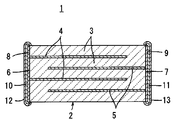
- multilayer ceramic capacitor 1 which is a typical example of the multilayer ceramic electronic component according to the present invention will be described.
- the multilayer ceramic capacitor 1 includes a multilayer body 2 including a plurality of laminated dielectric ceramic layers 3 and a plurality of internal electrodes 4 and 5 formed along a specific interface between the dielectric ceramic layers 3. I have.
- the first and second external electrodes 8 and 9 are formed on the end surfaces of the multilayer body 2 facing each other.
- the internal electrodes 4 and 5 are a plurality of first internal electrodes 4 electrically connected to the first external electrode 8 and a plurality of second internal electrodes 5 electrically connected to the second external electrode 9.
- the first and second internal electrodes 4 and 5 are alternately arranged in the stacking direction.
- a method is employed in which a dielectric ceramic green sheet and an internal electrode layer are laminated and fired at the same time in the manufacturing process.
- base metals such as Ni have been used for internal electrodes of multilayer ceramic capacitors in order to reduce costs.
- Patent Document 1 describes a multilayer ceramic body that employs Al as an internal electrode material that replaces Ni. By forming an Al 2 O 3 film on the surface layer portion of the Al internal electrode, mechanical characteristics and electrical properties can be obtained. The characteristic is improved.
- an object of the present invention is to provide a multilayer ceramic electronic component having a high capacitance while having an Al internal electrode excellent in smoothness and conductivity.
- the present invention provides a laminate comprising a plurality of laminated ceramic layers and a plurality of Al-based internal electrodes formed along a specific interface between the ceramic layers, and an outer surface of the laminate A multilayer ceramic electronic component including an external electrode formed thereon, wherein the surface of the internal electrode is covered with a layer mainly composed of a noble metal or Ti.
- the precious metal is preferably Ag.
- the main component of the ceramic layer is a barium titanate-based perovskite compound, and the multilayer ceramic electronic component is a multilayer ceramic capacitor.
- the dielectric constant of the ceramic layer is increased, which contributes to the improvement of the capacitance.
- the ceramic layer further contains an oxide containing Bi such as Bi 2 O 3 as a subcomponent.
- an oxide containing Bi such as Bi 2 O 3 as a subcomponent.
- the thickness of the Al 2 O 3 layer generated on the surface layer portion of the Al internal electrode is suppressed to the minimum necessary thickness for maintaining the mechanical characteristics, the dielectric constant of the Al 2 O 3 layer is low. Influence on the capacitance is reduced. Therefore, a multilayer ceramic electronic component having a high capacitance can be obtained.
- FIG. 1 is an enlarged view of a cross section of a multilayer ceramic capacitor as an example of the multilayer ceramic electronic component of the present invention.
- the main component of the internal electrode is Al.
- the internal electrode may be Al alone or an Al alloy, but when it is an Al alloy, the Al content is preferably 70 mol% or more, and more preferably 90 mol% or more.
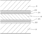
- FIG. 2 shows an enlarged view of a cross section of a multilayer ceramic capacitor which is an example of the present invention.
- the internal electrodes of the internal electrodes 4 and 5, the peripheral portion of the internal electrode 4 is shown as a representative.
- an Al 2 O 3 layer 21 is present on the surface layer of the internal electrode 4 containing Al as a main component. This is mainly due to the oxidation of the surface of the Al internal electrode 4.
- the Al 2 O 3 layer 21 has a function of smoothing the Al internal electrode 4 and a function of suppressing delamination between the ceramic layer 3 and the Al internal electrode 4. From this viewpoint, the thickness of the Al 2 O 3 layer 21 is preferably 0.25% or more of the thickness of the internal electrode. However, as described above, in order to ensure the capacitance, it is desirable that the thickness of the Al 2 O 3 layer 21 be kept as small as possible.
- a layer 22 mainly composed of noble metal or Ti is formed at the interface between the Al internal electrode 4 and the ceramic layer 3.
- the layer 22 mainly composed of the noble metal or Ti suppresses the oxidation of the Al internal electrode 4 and suppresses the increase in the thickness of the Al 2 O 3 layer 21.
- Ag is a typical noble metal, but Pd, Au, Pt, and alloys thereof may also be used.
- ceramic raw materials are prepared. This ceramic raw material is mixed with an organic binder component in a solvent as necessary to form a ceramic slurry. A ceramic green sheet is obtained by sheet-forming this ceramic slurry.
- a layer 22 mainly composed of noble metal or Ti is formed on the ceramic green sheet.
- a method of screen printing a paste containing noble metal powder or Ti powder and an organic vehicle in a desired pattern is simple.
- a layer of the Al internal electrode 4 is formed on the layer 22 mainly composed of noble metal or Ti.
- this method there are a method of applying an Al paste, a transfer method, a vacuum thin film forming method, and the like.
- a layer 22 mainly composed of noble metal or Ti is formed on the layer of the Al internal electrode 4.
- the ceramic green sheet, the layer 22 mainly composed of noble metal or Ti, the layer 4 of the Al internal electrode, the layer 22 mainly composed of noble metal or Ti are stacked in this order, and are subjected to pressure bonding. A raw laminate before firing is obtained.
- This raw laminate is fired in a firing furnace at a predetermined atmosphere and temperature.
- the oxygen partial pressure during firing is 1 ⁇ 10 ⁇ 4 MPa or more and the firing temperature is 600 ° C. or more, the oxidation of the surface of the Al internal electrode 4 proceeds, and the Al 2 O 3 layer 21 having an appropriate thickness. Produces. Further, for example, when the firing temperature is 1000 ° C. or less, the spheroidization of the Al internal electrode 4 is effectively prevented.
- the oxygen partial pressure atmospheric pressure is most preferable in consideration of the simplicity of the process.
- the layer 22 mainly composed of noble metal or Ti reduces the contact of the Al internal electrode 4 with oxygen, and as a result, the oxidation of the Al internal electrode 4 is suppressed to a desired level or less.
- a TiO 2 layer may be formed on the surface of Ti by firing. However, since this TiO 2 layer has low insulation, the capacitance decreases. Has little effect.
- the ceramic composition in the multilayer ceramic electronic component of the present invention is not particularly limited. Barium titanate (including those substituted with Ca, Sr, Zr, etc.), lead titanate or lead zirconate titanate, alumina glass ceramic, ferrite, transition element oxide semiconductor ceramic, etc. Various materials can be applied as long as the object of the invention is not impaired.
- the multilayer ceramic electronic component of the present invention is not limited to a multilayer ceramic capacitor, and can be applied to various electronic components such as a multilayer piezoelectric element, a multilayer thermistor element, a multilayer chip coil, and a ceramic multilayer substrate.
- BaTiO 3 powder was prepared as the main component of the ceramic, and Bi 2 O 3 and BaCO 3 powders were prepared as the subcomponents. These powders were mixed so as to have a composition of 100BaTiO 3 + 3Bi 2 O 3 + 2BaCO 3 to obtain a ceramic raw material.
- an ethanol-based organic solvent and a polyvinyl butyral-based binder were added and wet-mixed with a ball mill to obtain a ceramic slurry.
- This ceramic slurry was formed into a sheet to obtain a ceramic green sheet.
- the metal listed in Table 1 was formed on the ceramic green sheet by vacuum deposition so as to have the thickness shown in Table 1.
- an Al internal electrode layer was formed to a thickness of 0.6 ⁇ m by vacuum deposition.
- the metal of Table 1 was similarly formed into a film by the vacuum evaporation method so that it may become the thickness of Table 1.
- the ceramic green sheets formed with the Al internal electrodes covered with the metal film shown in Table 1 and formed as described above were laminated so that the drawn-out sides of the Al internal electrodes were staggered, pressure-bonded, and raw green A laminate was obtained.
- the raw laminate was heated in the atmosphere at 270 ° C. to remove the binder. Thereafter, the temperature was increased at a rate of temperature increase of 100 ° C./min, and firing was performed at 650 ° C. for 1 hour.
- An Ag paste containing a low-melting glass frit was applied to both end faces of the obtained laminate, and baked at 600 ° C. in the atmosphere to obtain an external electrode connected to the internal electrode.
- the multilayer ceramic capacitor obtained as described above has a length of 2.0 mm, a width of 1.0 mm, and a thickness of 0.5 mm, a ceramic layer thickness of 50 ⁇ m, an Al internal electrode layer thickness of 0.6 ⁇ m, and an effective layer.
- the number was 5.
- the capacitance of the obtained sample was measured using an automatic bridge type measuring device. The results are shown in Table 1. Moreover, the cross section obtained by FIB processing was analyzed by ⁇ -SAM, and the Al 2 O 3 layer in the cross section of the internal electrode was identified. The thickness of this Al 2 O 3 layer was measured at arbitrary 10 points, and the average thickness was determined. The results are also shown in Table 1.
- the multilayer ceramic electronic component of the present invention can be applied to multilayer ceramic capacitors, multilayer piezoelectric elements, multilayer thermistors, multilayer chip coils, ceramic multilayer substrates, and the like.
Landscapes
- Engineering & Computer Science (AREA)
- Power Engineering (AREA)
- Microelectronics & Electronic Packaging (AREA)
- Chemical & Material Sciences (AREA)
- Manufacturing & Machinery (AREA)
- Ceramic Engineering (AREA)
- Materials Engineering (AREA)
- Inorganic Chemistry (AREA)
- Physics & Mathematics (AREA)
- Electromagnetism (AREA)
- Fixed Capacitors And Capacitor Manufacturing Machines (AREA)
- Ceramic Capacitors (AREA)
Abstract
平滑性、導電性に優れるAl内部電極を備えつつ、高い静電容量を示す積層セラミック電子部品を提供する。 積層された複数のセラミック層と、前記セラミック層間の特定の界面に沿って形成される複数のAlを主成分とする内部電極とを備える積層体と、前記積層体の外表面上に形成された外部電極と、を含む積層セラミック電子部品であって、前記内部電極の表面が、貴金属またはTiを主成分とする層により被覆されている。
Description
本発明は、積層セラミックコンデンサに代表される積層セラミック電子部品に関し、特に、Alを主成分とする内部電極を備えるものに関する。
図1を参照して、まず、この発明に係る積層セラミック電子部品の代表例である積層セラミックコンデンサ1について説明する。
積層セラミックコンデンサ1は、積層された複数の誘電体セラミック層3と誘電体セラミック層3間の特定の界面に沿って形成される複数の内部電極4および5とをもって構成される、積層体2を備えている。
図1に示した積層セラミックコンデンサ1では、第1および第2の外部電極8および9は、積層体2の互いに対向する各端面上に形成される。内部電極4および5は、第1の外部電極8に電気的に接続される複数の第1の内部電極4と第2の外部電極9に電気的に接続される複数の第2の内部電極5とがあり、これら第1および第2の内部電極4および5は、積層方向に関して交互に配置されている。
積層セラミックコンデンサでは特に小型化が要求されるため、製造過程において、誘電体セラミックのグリーンシートと、内部電極層とを積層した後、同時に焼成する手法がとられる。近年、積層セラミックコンデンサの内部電極には、コスト削減のため、Ni等の卑金属が用いられている。
しかし、Niはセラミックとの共焼結時に非常に酸化されやすいため、焼成時の雰囲気を還元雰囲気とし、温度条件および酸素分圧を精密に制御する必要があった。結果として、材料設計に大きな制約が生じた。加えて、共焼成に伴う不均一な応力に起因するデラミネーションやクラック等の問題が懸念された。
よって、積層セラミック電子部品の設計の自由度を高めるためには、様々な金属種の内部電極が検討されることが好ましい。
たとえば、特許文献1には、Niに替わる内部電極材料としてAlを採用した積層セラミック体について述べており、Al内部電極の表層部にAl2O3膜を生成することにより、機械的特性および電気的特性を向上させている。
代表的な積層セラミック電子部品である積層セラミックコンデンサでは、増々、大容量化が望まれている。このような場合、特許文献1における積層セラミック電子部品においては、セラミック層とAl内部電極との界面に存在するAl2O3膜の誘電率が低いため、積層セラミック電子部品の静電容量が不足気味になる、という問題点があった。
そこで、本発明の目的は、平滑性、導電性に優れるAl内部電極を備えつつ、高い静電容量を示す積層セラミック電子部品を提供することにある。
すなわち本発明は、積層された複数のセラミック層と、前記セラミック層間の特定の界面に沿って形成される複数のAlを主成分とする内部電極とを備える積層体と、前記積層体の外表面上に形成された外部電極と、を含む積層セラミック電子部品であって、前記内部電極の表面が、貴金属またはTiを主成分とする層により被覆されていることを特徴とする。
前記貴金属は、Agであることが望ましい。
また、前記セラミック層の主成分がチタン酸バリウム系ペロブスカイト化合物であり、前記積層セラミック電子部品が積層セラミックコンデンサであることが望ましい。この場合、セラミック層の誘電率が高くなり、静電容量の向上に寄与する。
さらに、前記セラミック層が、さらに副成分としてBi2O3などのBiを含有する酸化物を含むことも好ましい。この場合、低温焼結が可能になり、内部電極の被覆率が向上し、静電容量の向上に寄与する。
本発明によれば、Al内部電極の表層部に生成するAl2O3層の厚みが、機械的特性を維持する必要最低限の厚みに抑えられるため、Al2O3層の誘電率の低さが静電容量に与える影響が低減される。よって、静電容量の高い積層セラミック電子部品を得ることができる。
本発明の積層セラミック電子部品は、その内部電極の主成分がAlである。この内部電極はAl単体でもAl合金でも良いが、Al合金である場合、Alの含有率が70モル%以上であることが好ましく、さらに好ましくは90モル%以上である。
図2では、本発明の例である積層セラミックコンデンサの断面の拡大図が示されている。内部電極については、内部電極4および5のうち、代表して内部電極4の周辺部を図示している。
Alを主成分とする内部電極4の表層には、Al2O3層21が存在することが多い。これは、主として、Al内部電極4の表面が酸化したことに因るものである。このAl2O3層21にはAl内部電極4を平滑にする作用があり、セラミック層3とAl内部電極4との間のデラミネーションを抑制する機能がある。この観点より、このAl2O3層21の厚みは内部電極の厚みの0.25%以上であることが好ましい。しかし、前述のように、静電容量を確保するためには、Al2O3層21の厚みが可能な限り小さく抑えられることが望ましい。
さらに、Al内部電極4とセラミック層3の界面には、貴金属またはTiを主成分とする層22が形成されている。この貴金属またはTiを主成分とする層22は、Al内部電極4の酸化を抑制し、Al2O3層21の厚みの増大を抑制する。貴金属として代表的なものにAgがあるが、その他、Pd、Au、Ptや、それらの合金でも構わない。
次に、本発明の積層セラミック電子部品の製造方法について、積層セラミックコンデンサを例にとり説明する。
まず、セラミック原料が用意される。このセラミック原料は、溶媒中にて必要に応じて有機バインダ成分と混合され、セラミックスラリーとされる。このセラミックスラリーをシート成形することにより、セラミックグリーンシートが得られる。
次に、貴金属またはTiを主成分とする層22がセラミックグリーンシート上に形成される。これにはいくつかの方法があり、貴金属粉やTi粉と有機ビヒクルとを含むペーストを所望のパターンにスクリーン印刷する方法が簡便である。その他にも、予め作製した箔を転写する方法や、真空薄膜形成法により成膜する方法もある。
次いで、Al内部電極4の層が、貴金属またはTiを主成分とする層22の上に形成される。この方法としても、Alペーストを塗布する方法や、転写、真空薄膜形成法などの方法がある。
そして、Al内部電極4の層の上に、再度、貴金属またはTiを主成分とする層22が形成される。
このようにして、セラミックグリーンシート、貴金属またはTiを主成分とする層22、Al内部電極の層4、貴金属またはTiを主成分とする層22、の順に多数層重ねられ、圧着することにより、焼成前の生の積層体が得られる。
この生の積層体は、焼成炉において、所定の雰囲気・温度にて焼成される。たとえば、焼成時の酸素分圧を1×10⁻⁴MPa以上とし、焼成温度を600℃以上とした場合、Al内部電極4の表面の酸化が進み、適度な厚みを有するAl2O3層21が生成する。また、たとえば、焼成温度を1000℃以下とすると、Al内部電極4の球状化が効果的に防がれる。酸素分圧に関しては、工程の簡便さを考慮すると、大気圧が最も好ましい。
このとき、貴金属またはTiを主成分とする層22が、Al内部電極4の酸素との接触を減らし、結果としてAl内部電極4の酸化を所望の程度以下に抑える。貴金属またはTiを主成分とする層22にTiを用いた場合、焼成によりTiの表面にTiO2層が生成することはあるが、このTiO2層は絶縁性が低いため、静電容量の低下には殆ど影響しない。
なお、本発明の積層セラミック電子部品におけるセラミック組成は特に限定されるものではない。チタン酸バリウム系(Ca、Sr、Zr等で置換されたものも含む)、チタン酸鉛系またはチタン酸ジルコン酸鉛系、アルミナ系ガラスセラミック、フェライト、遷移元素酸化物系半導体セラミック、など、本発明の目的を損なわない範囲で様々な材料を適用可能である。
また、本発明の積層セラミック電子部品は、積層セラミックコンデンサに限らず、積層型圧電素子、積層サーミスタ素子、積層チップコイル、セラミック多層基板など様々な電子部品に適用可能である。
本実施例は、あるチタン酸バリウム系のセラミックとAl内部電極とを用いた積層セラミックコンデンサにおいて、Al内部電極を被覆する層の金属種や厚みによる影響をみたものである。
まず、セラミックの主成分としてBaTiO3粉末を用意し、副成分としてBi2O3、BaCO3の粉末を用意した。これらの粉末を、100BaTiO3+3Bi2O3+2BaCO3の組成となるよう混合し、セラミック原料を得た。
このセラミック原料に、エタノール系の有機溶剤およびポリビニルブチラール系バインダを加え、ボールミルで湿式混合し、セラミックスラリーを得た。このセラミックスラリーをシート成形し、セラミックグリーンシートを得た。
次に、セラミックグリーンシート上に、表1に記載の金属を、真空蒸着法により、表1の厚みになるよう成膜した。次いで、真空蒸着法によりAl内部電極の層を0.6μmの厚みに形成した。さらにその上に、表1に記載の金属を、真空蒸着法により、表1の厚みになるよう同様に成膜した。
このようにして得た、表1の金属膜で被覆されたAl内部電極の形成されたセラミックグリーンシートを、Al内部電極の引き出されている側が互い違いになるように積層し、圧着し、生の積層体を得た。
この生の積層体を大気中にて270℃にて加熱し、バインダを除去した。この後、100℃/分の昇温速度にて昇温し、650℃において1時間焼成した。得られた積層体の両端面に低融点ガラスフリットを含有するAgペーストを塗布し、大気中にて600℃で焼き付け、これを内部電極と接続する外部電極とした。
以上のようにして得られた積層セラミックコンデンサは、長さ2.0mm、幅1.0mm厚さ0.5mmであり、セラミック層厚みは50μm、Al内部電極層の厚みは0.6μm、有効層数は5であった。
得られた試料について静電容量を自動ブリッジ式測定器を用い測定した。結果を表1に示した。また、また、FIB加工により得た断面をμ-SAMによって分析し、内部電極の断面におけるAl2O3層を同定した。このAl2O3層の厚みを任意の10点において測定し、その平均厚みを求めた。結果を併せて表1に示す。

表1の結果により、Al内部電極が、Ag、Tiで被覆された試料番号2~6の試料においては、高い静電容量が得られた。
Al内部電極に対する金属被覆を行わなかった試料番号1の試料においては、Al2O3層の厚みが大きかった影響で、期待していた静電容量が得られなかった。
Al内部電極がNiで被覆された試料番号7の試料においては、期待していた静電容量が得られなかった。これは、被覆金属であるNiが全て酸化してしまい、そこからAl内部電極の酸化が進み、結果としてAl2O3層の厚みが大きくなったためと考えられる。
本発明の積層セラミック電子部品は、積層セラミックコンデンサ、積層圧電素子、積層サーミスタ、積層チップコイル、セラミック多層基板などに応用が可能である。
1 積層セラミックコンデンサ
2 積層体
3 セラミック層
4、5 Al内部電極
6、7 積層体の端面
8、9 外部電極
10、11 第1のめっき層
12、13 第2のめっき層
21 Al2O3層
22 貴金属またはTiを主成分とする層
2 積層体
3 セラミック層
4、5 Al内部電極
6、7 積層体の端面
8、9 外部電極
10、11 第1のめっき層
12、13 第2のめっき層
21 Al2O3層
22 貴金属またはTiを主成分とする層
Claims (4)
- 積層された複数のセラミック層と、前記セラミック層間の特定の界面に沿って形成される複数のAlを主成分とする内部電極とを備える積層体と、前記積層体の外表面上に形成された外部電極と、を含む積層セラミック電子部品であって、
前記内部電極の表面が、貴金属またはTiを主成分とする層により被覆されていることを特徴とする、積層セラミック電子部品。 - 前記貴金属がAgである、請求項1に記載の積層セラミック電子部品。
- 前記セラミック層の主成分がチタン酸バリウム系ペロブスカイト化合物であり、前記積層セラミック電子部品が積層セラミックコンデンサである、請求項1または2に記載の積層セラミック電子部品。
- 前記セラミック層が、さらに副成分としてBiを含有する酸化物を含む、請求項1ないし3に記載の積層セラミック電子部品。
Priority Applications (2)
| Application Number | Priority Date | Filing Date | Title |
|---|---|---|---|
| JP2013520511A JP5641139B2 (ja) | 2011-06-17 | 2012-06-06 | 積層セラミック電子部品、および積層セラミック電子部品の製造方法 |
| US14/102,594 US9443654B2 (en) | 2011-06-17 | 2013-12-11 | Multilayer ceramic electronic component and method for manufacturing multilayer ceramic electronic component |
Applications Claiming Priority (2)
| Application Number | Priority Date | Filing Date | Title |
|---|---|---|---|
| JP2011-135284 | 2011-06-17 | ||
| JP2011135284 | 2011-06-17 |
Related Child Applications (1)
| Application Number | Title | Priority Date | Filing Date |
|---|---|---|---|
| US14/102,594 Continuation US9443654B2 (en) | 2011-06-17 | 2013-12-11 | Multilayer ceramic electronic component and method for manufacturing multilayer ceramic electronic component |
Publications (1)
| Publication Number | Publication Date |
|---|---|
| WO2012173018A1 true WO2012173018A1 (ja) | 2012-12-20 |
Family
ID=47357007
Family Applications (1)
| Application Number | Title | Priority Date | Filing Date |
|---|---|---|---|
| PCT/JP2012/064526 Ceased WO2012173018A1 (ja) | 2011-06-17 | 2012-06-06 | 積層セラミック電子部品、および積層セラミック電子部品の製造方法 |
Country Status (3)
| Country | Link |
|---|---|
| US (1) | US9443654B2 (ja) |
| JP (1) | JP5641139B2 (ja) |
| WO (1) | WO2012173018A1 (ja) |
Cited By (2)
| Publication number | Priority date | Publication date | Assignee | Title |
|---|---|---|---|---|
| JP2023150118A (ja) * | 2022-03-31 | 2023-10-16 | 太陽誘電株式会社 | セラミック電子部品およびその製造方法 |
| WO2024185341A1 (ja) * | 2023-03-07 | 2024-09-12 | 太陽誘電株式会社 | 積層セラミック電子部品 |
Families Citing this family (5)
| Publication number | Priority date | Publication date | Assignee | Title |
|---|---|---|---|---|
| JP6954519B2 (ja) * | 2017-04-11 | 2021-10-27 | 太陽誘電株式会社 | 積層セラミックコンデンサ |
| US20220122771A1 (en) * | 2020-10-19 | 2022-04-21 | Imagine Tf, Llc | Layered capacitor with two different types of electrode material |
| JP7657003B2 (ja) * | 2021-05-31 | 2025-04-04 | 太陽誘電株式会社 | セラミック電子部品 |
| KR20230117793A (ko) | 2022-02-03 | 2023-08-10 | 삼성전기주식회사 | 적층형 전자 부품 |
| KR20240084127A (ko) | 2022-12-06 | 2024-06-13 | 삼성전기주식회사 | 적층형 전자 부품 및 그 제조방법 |
Citations (4)
| Publication number | Priority date | Publication date | Assignee | Title |
|---|---|---|---|---|
| JPS6453519A (en) * | 1987-08-25 | 1989-03-01 | Matsushita Electric Industrial Co Ltd | Laminated ceramic capacitor and its manufacture |
| JPH113834A (ja) * | 1996-07-25 | 1999-01-06 | Murata Mfg Co Ltd | 積層セラミックコンデンサおよびその製造方法 |
| JP2008229849A (ja) * | 2007-03-16 | 2008-10-02 | Murata Mfg Co Ltd | 誘電体フィルムおよびそれを用いた電子部品 |
| JP2011097016A (ja) * | 2009-09-30 | 2011-05-12 | Murata Mfg Co Ltd | 積層セラミック電子部品、および積層セラミック電子部品の製造方法 |
Family Cites Families (2)
| Publication number | Priority date | Publication date | Assignee | Title |
|---|---|---|---|---|
| JPH10241991A (ja) * | 1997-02-24 | 1998-09-11 | Taiyo Yuden Co Ltd | 積層コンデンサとそのトリミング方法 |
| JP4295179B2 (ja) * | 2004-08-31 | 2009-07-15 | Tdk株式会社 | 電子部品およびその製造方法 |
-
2012
- 2012-06-06 WO PCT/JP2012/064526 patent/WO2012173018A1/ja not_active Ceased
- 2012-06-06 JP JP2013520511A patent/JP5641139B2/ja active Active
-
2013
- 2013-12-11 US US14/102,594 patent/US9443654B2/en active Active
Patent Citations (4)
| Publication number | Priority date | Publication date | Assignee | Title |
|---|---|---|---|---|
| JPS6453519A (en) * | 1987-08-25 | 1989-03-01 | Matsushita Electric Industrial Co Ltd | Laminated ceramic capacitor and its manufacture |
| JPH113834A (ja) * | 1996-07-25 | 1999-01-06 | Murata Mfg Co Ltd | 積層セラミックコンデンサおよびその製造方法 |
| JP2008229849A (ja) * | 2007-03-16 | 2008-10-02 | Murata Mfg Co Ltd | 誘電体フィルムおよびそれを用いた電子部品 |
| JP2011097016A (ja) * | 2009-09-30 | 2011-05-12 | Murata Mfg Co Ltd | 積層セラミック電子部品、および積層セラミック電子部品の製造方法 |
Cited By (2)
| Publication number | Priority date | Publication date | Assignee | Title |
|---|---|---|---|---|
| JP2023150118A (ja) * | 2022-03-31 | 2023-10-16 | 太陽誘電株式会社 | セラミック電子部品およびその製造方法 |
| WO2024185341A1 (ja) * | 2023-03-07 | 2024-09-12 | 太陽誘電株式会社 | 積層セラミック電子部品 |
Also Published As
| Publication number | Publication date |
|---|---|
| US9443654B2 (en) | 2016-09-13 |
| JPWO2012173018A1 (ja) | 2015-02-23 |
| US20140175942A1 (en) | 2014-06-26 |
| JP5641139B2 (ja) | 2014-12-17 |
Similar Documents
| Publication | Publication Date | Title |
|---|---|---|
| JP7148239B2 (ja) | セラミック電子部品およびその製造方法 | |
| JP5483498B2 (ja) | 積層セラミック電子部品及びその製造方法 | |
| JP5293971B2 (ja) | 積層セラミック電子部品、および積層セラミック電子部品の製造方法 | |
| JP5825322B2 (ja) | 積層セラミックキャパシタ、その製造方法及び積層セラミックキャパシタの実装基板 | |
| JP5641139B2 (ja) | 積層セラミック電子部品、および積層セラミック電子部品の製造方法 | |
| JP5780856B2 (ja) | 積層セラミックコンデンサ | |
| JP5527404B2 (ja) | 積層セラミック電子部品 | |
| JP2019192862A (ja) | 積層セラミックコンデンサおよびその製造方法 | |
| JP5527405B2 (ja) | 積層セラミック電子部品 | |
| CN118824729A (zh) | 多层电子组件 | |
| JP5527403B2 (ja) | 積層セラミック電子部品 | |
| JP5527400B2 (ja) | 積層セラミック電子部品 | |
| JP5527401B2 (ja) | 積層セラミック電子部品 | |
| JP2023143031A (ja) | セラミック電子部品およびその製造方法 | |
| JP5429393B2 (ja) | 積層セラミック電子部品、および積層セラミック電子部品の製造方法 | |
| JP5527402B2 (ja) | 積層セラミック電子部品 |
Legal Events
| Date | Code | Title | Description |
|---|---|---|---|
| 121 | Ep: the epo has been informed by wipo that ep was designated in this application |
Ref document number: 12800681 Country of ref document: EP Kind code of ref document: A1 |
|
| ENP | Entry into the national phase |
Ref document number: 2013520511 Country of ref document: JP Kind code of ref document: A |
|
| NENP | Non-entry into the national phase |
Ref country code: DE |
|
| 122 | Ep: pct application non-entry in european phase |
Ref document number: 12800681 Country of ref document: EP Kind code of ref document: A1 |