WO2012172959A1 - 粘着シート及び電子部品の製造方法 - Google Patents
粘着シート及び電子部品の製造方法 Download PDFInfo
- Publication number
- WO2012172959A1 WO2012172959A1 PCT/JP2012/063630 JP2012063630W WO2012172959A1 WO 2012172959 A1 WO2012172959 A1 WO 2012172959A1 JP 2012063630 W JP2012063630 W JP 2012063630W WO 2012172959 A1 WO2012172959 A1 WO 2012172959A1
- Authority
- WO
- WIPO (PCT)
- Prior art keywords
- pressure
- sensitive adhesive
- adhesive layer
- adhesive sheet
- elastic modulus
- Prior art date
- Legal status (The legal status is an assumption and is not a legal conclusion. Google has not performed a legal analysis and makes no representation as to the accuracy of the status listed.)
- Ceased
Links
Images

Classifications
-
- H—ELECTRICITY
- H10—SEMICONDUCTOR DEVICES; ELECTRIC SOLID-STATE DEVICES NOT OTHERWISE PROVIDED FOR
- H10P—GENERIC PROCESSES OR APPARATUS FOR THE MANUFACTURE OR TREATMENT OF DEVICES COVERED BY CLASS H10
- H10P72/00—Handling or holding of wafers, substrates or devices during manufacture or treatment thereof
- H10P72/70—Handling or holding of wafers, substrates or devices during manufacture or treatment thereof for supporting or gripping
- H10P72/74—Handling or holding of wafers, substrates or devices during manufacture or treatment thereof for supporting or gripping using temporarily an auxiliary support
- H10P72/7402—Wafer tapes, e.g. grinding or dicing support tapes
-
- C—CHEMISTRY; METALLURGY
- C08—ORGANIC MACROMOLECULAR COMPOUNDS; THEIR PREPARATION OR CHEMICAL WORKING-UP; COMPOSITIONS BASED THEREON
- C08L—COMPOSITIONS OF MACROMOLECULAR COMPOUNDS
- C08L63/00—Compositions of epoxy resins; Compositions of derivatives of epoxy resins
- C08L63/10—Epoxy resins modified by unsaturated compounds
-
- C—CHEMISTRY; METALLURGY
- C09—DYES; PAINTS; POLISHES; NATURAL RESINS; ADHESIVES; COMPOSITIONS NOT OTHERWISE PROVIDED FOR; APPLICATIONS OF MATERIALS NOT OTHERWISE PROVIDED FOR
- C09J—ADHESIVES; NON-MECHANICAL ASPECTS OF ADHESIVE PROCESSES IN GENERAL; ADHESIVE PROCESSES NOT PROVIDED FOR ELSEWHERE; USE OF MATERIALS AS ADHESIVES
- C09J163/00—Adhesives based on epoxy resins; Adhesives based on derivatives of epoxy resins
- C09J163/10—Epoxy resins modified by unsaturated compounds
-
- C—CHEMISTRY; METALLURGY
- C09—DYES; PAINTS; POLISHES; NATURAL RESINS; ADHESIVES; COMPOSITIONS NOT OTHERWISE PROVIDED FOR; APPLICATIONS OF MATERIALS NOT OTHERWISE PROVIDED FOR
- C09J—ADHESIVES; NON-MECHANICAL ASPECTS OF ADHESIVE PROCESSES IN GENERAL; ADHESIVE PROCESSES NOT PROVIDED FOR ELSEWHERE; USE OF MATERIALS AS ADHESIVES
- C09J7/00—Adhesives in the form of films or foils
- C09J7/20—Adhesives in the form of films or foils characterised by their carriers
-
- C—CHEMISTRY; METALLURGY
- C08—ORGANIC MACROMOLECULAR COMPOUNDS; THEIR PREPARATION OR CHEMICAL WORKING-UP; COMPOSITIONS BASED THEREON
- C08L—COMPOSITIONS OF MACROMOLECULAR COMPOUNDS
- C08L2205/00—Polymer mixtures characterised by other features
- C08L2205/05—Polymer mixtures characterised by other features containing polymer components which can react with one another
-
- C—CHEMISTRY; METALLURGY
- C09—DYES; PAINTS; POLISHES; NATURAL RESINS; ADHESIVES; COMPOSITIONS NOT OTHERWISE PROVIDED FOR; APPLICATIONS OF MATERIALS NOT OTHERWISE PROVIDED FOR
- C09J—ADHESIVES; NON-MECHANICAL ASPECTS OF ADHESIVE PROCESSES IN GENERAL; ADHESIVE PROCESSES NOT PROVIDED FOR ELSEWHERE; USE OF MATERIALS AS ADHESIVES
- C09J2203/00—Applications of adhesives in processes or use of adhesives in the form of films or foils
- C09J2203/326—Applications of adhesives in processes or use of adhesives in the form of films or foils for bonding electronic components such as wafers, chips or semiconductors
-
- C—CHEMISTRY; METALLURGY
- C09—DYES; PAINTS; POLISHES; NATURAL RESINS; ADHESIVES; COMPOSITIONS NOT OTHERWISE PROVIDED FOR; APPLICATIONS OF MATERIALS NOT OTHERWISE PROVIDED FOR
- C09J—ADHESIVES; NON-MECHANICAL ASPECTS OF ADHESIVE PROCESSES IN GENERAL; ADHESIVE PROCESSES NOT PROVIDED FOR ELSEWHERE; USE OF MATERIALS AS ADHESIVES
- C09J2301/00—Additional features of adhesives in the form of films or foils
- C09J2301/10—Additional features of adhesives in the form of films or foils characterized by the structural features of the adhesive tape or sheet
- C09J2301/12—Additional features of adhesives in the form of films or foils characterized by the structural features of the adhesive tape or sheet by the arrangement of layers
- C09J2301/122—Additional features of adhesives in the form of films or foils characterized by the structural features of the adhesive tape or sheet by the arrangement of layers the adhesive layer being present only on one side of the carrier, e.g. single-sided adhesive tape
-
- C—CHEMISTRY; METALLURGY
- C09—DYES; PAINTS; POLISHES; NATURAL RESINS; ADHESIVES; COMPOSITIONS NOT OTHERWISE PROVIDED FOR; APPLICATIONS OF MATERIALS NOT OTHERWISE PROVIDED FOR
- C09J—ADHESIVES; NON-MECHANICAL ASPECTS OF ADHESIVE PROCESSES IN GENERAL; ADHESIVE PROCESSES NOT PROVIDED FOR ELSEWHERE; USE OF MATERIALS AS ADHESIVES
- C09J2301/00—Additional features of adhesives in the form of films or foils
- C09J2301/30—Additional features of adhesives in the form of films or foils characterized by the chemical, physicochemical or physical properties of the adhesive or the carrier
- C09J2301/312—Additional features of adhesives in the form of films or foils characterized by the chemical, physicochemical or physical properties of the adhesive or the carrier parameters being the characterizing feature
-
- C—CHEMISTRY; METALLURGY
- C09—DYES; PAINTS; POLISHES; NATURAL RESINS; ADHESIVES; COMPOSITIONS NOT OTHERWISE PROVIDED FOR; APPLICATIONS OF MATERIALS NOT OTHERWISE PROVIDED FOR
- C09J—ADHESIVES; NON-MECHANICAL ASPECTS OF ADHESIVE PROCESSES IN GENERAL; ADHESIVE PROCESSES NOT PROVIDED FOR ELSEWHERE; USE OF MATERIALS AS ADHESIVES
- C09J2301/00—Additional features of adhesives in the form of films or foils
- C09J2301/40—Additional features of adhesives in the form of films or foils characterized by the presence of essential components
- C09J2301/416—Additional features of adhesives in the form of films or foils characterized by the presence of essential components use of irradiation
-
- C—CHEMISTRY; METALLURGY
- C09—DYES; PAINTS; POLISHES; NATURAL RESINS; ADHESIVES; COMPOSITIONS NOT OTHERWISE PROVIDED FOR; APPLICATIONS OF MATERIALS NOT OTHERWISE PROVIDED FOR
- C09J—ADHESIVES; NON-MECHANICAL ASPECTS OF ADHESIVE PROCESSES IN GENERAL; ADHESIVE PROCESSES NOT PROVIDED FOR ELSEWHERE; USE OF MATERIALS AS ADHESIVES
- C09J2433/00—Presence of (meth)acrylic polymer
-
- H—ELECTRICITY
- H10—SEMICONDUCTOR DEVICES; ELECTRIC SOLID-STATE DEVICES NOT OTHERWISE PROVIDED FOR
- H10P—GENERIC PROCESSES OR APPARATUS FOR THE MANUFACTURE OR TREATMENT OF DEVICES COVERED BY CLASS H10
- H10P72/00—Handling or holding of wafers, substrates or devices during manufacture or treatment thereof
- H10P72/70—Handling or holding of wafers, substrates or devices during manufacture or treatment thereof for supporting or gripping
- H10P72/74—Handling or holding of wafers, substrates or devices during manufacture or treatment thereof for supporting or gripping using temporarily an auxiliary support
- H10P72/7416—Handling or holding of wafers, substrates or devices during manufacture or treatment thereof for supporting or gripping using temporarily an auxiliary support used during dicing or grinding
-
- H—ELECTRICITY
- H10—SEMICONDUCTOR DEVICES; ELECTRIC SOLID-STATE DEVICES NOT OTHERWISE PROVIDED FOR
- H10P—GENERIC PROCESSES OR APPARATUS FOR THE MANUFACTURE OR TREATMENT OF DEVICES COVERED BY CLASS H10
- H10P72/00—Handling or holding of wafers, substrates or devices during manufacture or treatment thereof
- H10P72/70—Handling or holding of wafers, substrates or devices during manufacture or treatment thereof for supporting or gripping
- H10P72/74—Handling or holding of wafers, substrates or devices during manufacture or treatment thereof for supporting or gripping using temporarily an auxiliary support
- H10P72/744—Details of chemical or physical process used for separating the auxiliary support from a device or a wafer
Definitions
- the present invention relates to a pressure-sensitive adhesive sheet and a method for producing an electronic component using the pressure-sensitive adhesive sheet.
- the adhesive sheet is usually bonded after the circuit is formed, and then cut into element pieces (dicing), washed, dried, stretched (expanded) the adhesive sheet, and peeled off the element pieces from the adhesive sheet. (Pickup), mounting and other processes.
- the pressure-sensitive adhesive sheet (dicing tape) used in these processes has sufficient adhesive force against the cut element chips (chips) from the dicing process to the drying process, but has no adhesive residue during the pick-up process. It is desired that the adhesive strength is reduced to a certain extent.
- the pressure-sensitive adhesive sheet there is one in which a pressure-sensitive adhesive layer that undergoes a polymerization and curing reaction by ultraviolet light or the like is coated on a base material that is transparent to active rays such as ultraviolet rays and / or electron beams.
- a pressure-sensitive adhesive layer that undergoes a polymerization and curing reaction by ultraviolet light or the like is coated on a base material that is transparent to active rays such as ultraviolet rays and / or electron beams.
- ultraviolet light or the like is irradiated to the pressure-sensitive adhesive layer, the pressure-sensitive adhesive layer is polymerized and cured to reduce the pressure-sensitive adhesive force, and then a cut chip is picked up.
- Patent Document 1 and Patent Document 2 disclose a compound having a photopolymerizable unsaturated double bond in its molecule (polyfunctional) that can be three-dimensionally reticulated on the substrate surface by, for example, actinic rays.
- An adhesive sheet coated with an adhesive containing an oligomer) is disclosed.
- the chip is peeled off from the adhesive sheet by pushing the needle pin against the adhesive sheet side of the semiconductor wafer after dicing and pushing up the cut and separated chip.
- the pressure-sensitive adhesive layer of the pressure-sensitive adhesive sheet may break due to the needle pin being pushed up.
- the broken pressure-sensitive adhesive layer adheres to the chip (adhesive residue), causing contamination and defective mounting processes.
- the main object of the present invention is to provide a pressure-sensitive adhesive sheet in which the adhesive strength before and after curing of the ultraviolet curable pressure-sensitive adhesive layer is in a preferable range and does not cause cracking of the pressure-sensitive adhesive layer during pickup.
- the present invention is a pressure-sensitive adhesive sheet comprising a base material and a photocurable pressure-sensitive adhesive layer formed on one side of the base material, and the photo-curing of the pressure-sensitive adhesive layer measured under the following conditions
- Adhesive having a storage modulus after storage of 0.5 to 2.0 ( ⁇ 10 8 Pa) and a storage elastic modulus after photocuring of the pressure-sensitive adhesive layer / storage elastic modulus of the substrate of 1 to 3
- the inventors of the present invention first paid attention to the storage elastic modulus after photocuring of the pressure-sensitive adhesive layer, and found that the pressure-sensitive adhesive layer cracks when the storage elastic modulus falls outside the specified range. However, even when the storage elastic modulus is within the specified range, an example of cracking of the pressure-sensitive adhesive layer has been found, and further investigation has been carried out. As a result, the storage elastic modulus after photocuring of the pressure-sensitive adhesive layer / base material It was found that such a crack occurs when the storage elastic modulus value of is out of the specified range.
- the storage elastic modulus after photocuring of the pressure-sensitive adhesive layer is within a specified range, and the storage elastic modulus after photocuring of the pressure-sensitive adhesive layer / the storage elastic modulus of the base material. It was found that by making the value within the specified range, cracking of the pressure-sensitive adhesive layer could be prevented, and the present invention was completed.
- the pressure-sensitive adhesive composition forming the pressure-sensitive adhesive layer comprises (meth) acrylic acid ester polymer (A), bisphenol A type epoxy acrylate (B), photopolymerization initiator (C), curing agent ( D), (B) is a tri- to tetra-functional acrylate, has a molecular weight of 1000 to 2000, and (D) has a tri- or higher functional isocyanate group, and is a hydroxyl group in the pressure-sensitive adhesive composition.
- the molar ratio of / isocyanate group is preferably 0.6 to 1.2.
- the weight average molecular weight of the (meth) acrylic acid ester polymer (A) is preferably 700,000 to 1,500,000.
- the storage elastic modulus of the substrate is, for example, 0.5 to 2.0 ( ⁇ 10 8 Pa).
- the storage elastic modulus of the pressure-sensitive adhesive after photocuring is preferably 0.5 to 1.5 ( ⁇ 10 8 Pa).
- the present invention also includes a bonding step of bonding an electronic component to the pressure-sensitive adhesive sheet, a dicing step of dicing the electronic component after the bonding step, and a base material pressure-sensitive adhesive layer after the dicing step.
- a method of manufacturing an electronic component including a pickup step of irradiating light from a non-surface side and picking up the electronic component from an adhesive layer.
- a pressure-sensitive adhesive sheet in which the adhesive strength before and after curing of the ultraviolet curable pressure-sensitive adhesive layer is in a preferable range, and the pressure-sensitive adhesive layer does not crack during pickup.
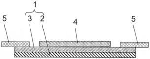
- FIG. 1 is a schematic cross-sectional view showing the configuration of an adhesive sheet according to the present invention.
- the pressure-sensitive adhesive sheet 1 includes a base material 2 and a photocurable pressure-sensitive adhesive layer 3 laminated on one side of the base material 2.
- the base material 2 is made of a material that is transmissive to actinic rays (hereinafter also simply referred to as “light”) such as ultraviolet rays and / or electron beams.
- light such as ultraviolet rays and / or electron beams.
- the material of the substrate 2 include the following. Polyvinyl chloride, polyethylene terephthalate, ethylene-vinyl acetate copolymer, ethylene-acrylic acid-acrylic acid ester film, ethylene-ethyl acrylate copolymer, polyethylene, polypropylene, ethylene-acrylic acid copolymer.
- (meth) acrylic acid means acrylic acid and methacrylic acid
- (meth) acryloyl group means acryloyl group and methacryloyl group.
- the substrate 2 may be a single layer or multilayer film or sheet made of the above-mentioned material, or may be a laminate of films made of different materials.
- the base material 2 is preferably subjected to an antistatic treatment.
- an antistatic treatment there are a treatment for adding an antistatic agent to the substrate 2, a treatment for applying an antistatic agent to the surface of the substrate 2, and a treatment by corona discharge.
- antistatic agent for example, a quaternary amine salt monomer can be used.
- Examples of the quaternary amine salt monomer include dimethylaminoethyl (meth) acrylate quaternary chloride, diethylaminoethyl (meth) acrylate quaternary chloride, methylethylaminoethyl (meth) acrylate quaternary chloride, p-dimethyl.
- Examples include aminostyrene quaternary chloride and p-diethylaminostyrene quaternary chloride. Of these, dimethylaminoethyl methacrylate quaternary chloride is preferred.
- the thickness of the substrate 2 is 50 to 200 ⁇ m, preferably 70 to 150 ⁇ m.
- the base material 2 has a storage elastic modulus G ′ of, for example, 0.2 to 2.0 ( ⁇ 10 8 Pa) or 0.5 to 2.0 ( ⁇ 10 8 Pa).
- the storage elastic modulus G ′ is, for example, 0.2, 0.3, 0.4, 0.5, 0.6, 0.7, 0.8, 0.9, 1.0, 1 .1, 1.2, 1.3, 1.4, 1.5, 1.6, 1.7, 1.8, 1.9, 2.0 ( ⁇ 10 8 Pa), illustrated here It may be within a range between any two of the numerical values.
- the storage elastic modulus G ′ of the substrate 2 can be adjusted by appropriately selecting and changing the material and thickness of the substrate 2.
- the pressure-sensitive adhesive layer 3 may be a photocurable type, and its composition is not particularly limited.
- the pressure-sensitive adhesive layer 3 is composed of (meth) acrylic acid ester polymer (A), bisphenol. It can be formed by an adhesive composition containing an A-type epoxy acrylate (B), a photopolymerization initiator (C), and a curing agent (D).
- the (meth) acrylic acid ester polymer (A) is a polymer obtained by polymerizing a (meth) acrylic acid ester monomer, and preferably has a weight average molecular weight of 500,000 to 2,000,000, More preferably, it is ⁇ 1.5 million. Further, the (meth) acrylic acid ester polymer may contain a vinyl compound monomer other than the (meth) acrylic acid ester monomer.
- weight average molecular weight is the value measured as a polystyrene conversion value by the gel permeation chromatography method (GPC).
- (Meth) acrylic acid ester monomers include n-butyl (meth) acrylate, 2-butyl (meth) acrylate, t-butyl (meth) acrylate, pentyl (meth) acrylate, octyl (meth) acrylate, 2 -Ethylhexyl acrylate, nonyl (meth) acrylate, decyl (meth) acrylate, lauryl (meth) acrylate, methyl (meth) acrylate, ethyl (meth) acrylate, isopropyl (meth) acrylate, tridecyl (meth) acrylate, myristyl ( (Meth) acrylate, cetyl (meth) acrylate, stearyl (meth) acrylate, cyclohexyl (meth) acrylate, isobornyl (meth) acrylate, dicyclopentanyl (meth) acrylate,
- vinyl compound monomers copolymerizable with (meth) acrylic acid ester monomers include vinyl acetate, vinyl alcohol, (meth) acrylic acid, crotonic acid, maleic acid, maleic anhydride, itaconic acid, fumaric acid And acid, acrylamide N-glycolic acid, cinnamic acid and the like.
- Bisphenol A type epoxy acrylate (B) is represented by the following formula.
- R represents a hydrogen atom or a (meth) acrylate group.
- N represents an integer of 1 or more.
- the bisphenol A type epoxy acrylate (B) is preferably a tri- to tetra-functional acrylate, and preferably has a molecular weight of 1000 to 2000.
- the peelability (pickup property) between the chip and the sheet at the time of pickup tends to decrease, and if it exceeds 4 functionalities, the adhesive layer cracks. Tend to.
- the pressure-sensitive adhesive layer tends to crack during pickup, and if it exceeds 2000, the pickup property tends to be lowered.
- the compounding quantity of bisphenol A type epoxy acrylate (B) shall be 20 to 200 mass parts with respect to 100 mass parts of (meth) acrylic acid ester polymer (A). If the blending amount is less than 20 parts by mass, the pick-up property tends to decrease, and if it exceeds 200 parts by mass, the adhesive layer is scraped up in the dicing process, and the adhesive layer thus scooped up is accurate in the pickup process. May cause degradation.
- the blending amount is, for example, 20, 40, 60, 80, 100, 120, 140, 160, 180, 200 parts by mass with respect to 100 parts by mass of the (meth) acrylic acid ester polymer (A). It may be within the range between any two of the numerical values exemplified here.
- benzoin benzoin alkyl ethers
- acetophenones anthraquinones
- thioxanthones ketals
- benzophenones or xanthones are used.
- benzoin examples include benzoin, benzoin methyl ether, benzoin ethyl ether, and benzoin propyl ether.
- acetophenones examples include benzoin alkyl ethers, acetophenone, 2,2-dimethoxy-2-phenylacetophenone, 2,2-diethoxy-2-phenylacetophenone, 1,1-dichloroacetophenone, and the like.
- Anthraquinones include 2-methylanthraquinone, 2-ethylanthraquinone, 2-tertiarybutylanthraquinone, 1-chloroanthraquinone and the like.
- Examples of thioxanthones include 2,4-dimethylthioxanthone, 2,4-diisopropylthioxanthone, and 2-chlorothioxanthone.
- Examples of ketals include acetophenone dimethyl ketal, benzyl dimethyl ketal, benzyl phenyl sulfide, tetramethyl thiuram monosulfide, azobisisobutyronitrile, dibenzyl, diacetyl, ⁇ -chloranthraquinone, and the like.
- photopolymerization initiator (C) conventionally known photopolymerization accelerators may be used alone or in combination of two or more as required.
- group, a tertiary amine, etc. can be used for a photoinitiator.
- the tertiary amine include triethylamine, tetraethylpentamine, dimethylamino ether and the like.
- the compounding quantity of a photoinitiator (C) shall be 1 to 5 mass parts with respect to 100 mass parts of (meth) acrylic acid ester polymer (A). If the blending amount is less than 1 part by mass, the pick-up property tends to decrease, and if it exceeds 5 parts by mass, the pressure-sensitive adhesive layer tends to crack.
- trimers such as aromatic diisocyanate, alicyclic diisocyanate and aliphatic diisocyanate are used. Further, trimethylolpropane adducts of these diisocyanates, burettes reacted with water, trimers having an isocyanurate ring, and the like are also preferably used.
- Examples of the aromatic diisocyanate include tolylene diisocyanate, 4,4-diphenylmethane diisocyanate, xylylene diisocyanate, and the like.
- Examples of the alicyclic diisocyanate include isophorone diisocyanate and methylene bis (4-cyclohexyl isocyanate).
- Examples of the aliphatic diisocyanate include hexamethylene diisocyanate and trimethylhexamethylene diisocyanate.
- the amount of the curing agent (D) is determined so that the molar ratio of hydroxyl group / isocyanate group in the pressure-sensitive adhesive composition is 0.6 to 1.2. If the molar ratio is less than 0.6, the pressure-sensitive adhesive layer tends to crack, and if it exceeds 1.2, the tape quality may be deteriorated due to a change with time during storage. Specifically, this molar ratio is, for example, 0.6, 0.7, 0.8, 0.9, 1.0, 1.1, 1.2, and any one of the numerical values exemplified here is 2 It may be within a range between the two.
- the adhesive composition may contain various additives such as a tackifier, a release agent, a softener, an anti-aging agent, a filler, an ultraviolet absorber, and a light stabilizer.
- rosin resin terpene resin, aliphatic petroleum resin, aromatic petroleum resin, hydrogenated petroleum resin, chroman indene resin, styrene resin, xylene resin and a mixture of these resins are used. These are resins that do not contain hydroxyl groups in their chemical structure.
- the thickness of the pressure-sensitive adhesive layer 3 is not particularly limited, but is, for example, 1 to 100 ⁇ m, preferably 2 to 40 ⁇ m. If the pressure-sensitive adhesive layer 3 is too thick, the pressure-sensitive adhesive force becomes too high and the pick-up property is lowered. On the other hand, if the pressure-sensitive adhesive layer 3 is too thin, the adhesive strength becomes too low, the chip retainability during dicing is lowered, and peeling may occur between the ring frame and the sheet. Specifically, the thickness of the pressure-sensitive adhesive layer 3 is, for example, 1, 2, 5, 10, 15, 20, 40, 50, 100 ⁇ m, and is within a range between any two of the numerical values exemplified here. May be.
- the pressure-sensitive adhesive layer 3 has a storage elastic modulus G ′ after photocuring of 0.5 to 2.0 ( ⁇ 10 8 Pa) and 0.5 to 1.5 ( ⁇ 10 8 Pa). It is preferable to do so. If the storage elastic modulus G ′ is less than 0.5 ⁇ 10 8 Pa, the peelability between the sheet and the adherend in the pick-up process tends to decrease, and if it exceeds 2.0 ⁇ 10 8 Pa, the needle pin Cracking of the pressure-sensitive adhesive layer due to push-up tends to occur. Specifically, the storage elastic modulus G ′ after the polymerization curing reaction of the pressure-sensitive adhesive layer 3 is, for example, 0.5, 0.6, 0.7, 0.8, 0.9, 1.0, 1.1. 1.2, 1.3, 1.4, 1.5, 1.6, 1.7, 1.8, 1.9, 2.0 ( ⁇ 10 8 Pa), and the numerical values exemplified here It may be within the range between any two.
- the storage elastic modulus G ′ after photocuring of the pressure-sensitive adhesive layer 3 is the blending amount of bisphenol A type epoxy acrylate (B), photopolymerization initiator (C), curing agent (D), (meth) acrylic acid ester polymer.
- the desired values can be set. Among these, it is important to set the functional number and molecular weight of the bisphenol A type epoxy acrylate (B) to predetermined values in order to obtain the desired post-curing elasticity by controlling the reaction amount of the photopolymerization reaction.
- the value of the ratio of the storage elastic modulus after photocuring of the pressure-sensitive adhesive layer / the storage elastic modulus of the substrate is 1 to 3, and preferably 2 to 3. That is, it is important that the storage elastic modulus of the pressure-sensitive adhesive layer after photocuring is the same as or slightly larger than that of the substrate. It was experimentally found that adhesive cracking is prevented by setting this value within such a range. In addition, when the storage elastic modulus after photocuring of an adhesive layer was smaller than the storage elastic modulus of a base material, or when the value of the said ratio was larger than 3, the crack of the adhesive occurred.
- FIGS. 1 to 4 show cross-sectional schematic diagrams of the steps of the electronic component manufacturing method according to the present invention.
- the electronic component manufacturing method according to the present invention includes a bonding step of bonding the electronic component to the above-described pressure-sensitive adhesive sheet 1, a dicing step of dicing the electronic component, irradiating ultraviolet rays from the substrate 2 side, A pickup step of picking up from the pressure-sensitive adhesive layer 3.
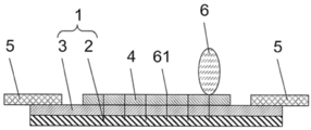
- the wafer or package 4 (hereinafter referred to as “wafer 4”) is bonded and fixed to the surface of the pressure-sensitive adhesive sheet 1, and the pressure-sensitive adhesive sheet 1 is fixed to the ring frame 5.
- the wafer 4 may be a conventional general-purpose wafer such as a silicon wafer, a gallium nitride wafer, a silicon carbide wafer, or a sapphire wafer.
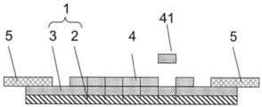
- FIG. 3 shows the state of the pressure-sensitive adhesive sheet 1 and the wafer 4 in the pickup process.
- FIG. 4 shows the state of the chip 41 after the pickup process.
- the ultraviolet light source a low-pressure mercury lamp, a high-pressure mercury lamp, an ultra-high pressure mercury lamp, or a metal halide lamp can be used.
- an electron beam, an alpha ray, a beta ray, and a gamma ray can be used as an electron beam light source.
- the light-sensitive adhesive layer 3 is three-dimensionally reticulated and cured by light irradiation, and the pressure-sensitive adhesive force of the pressure-sensitive adhesive layer 3 decreases. Due to the decrease in the adhesive strength of the pressure-sensitive adhesive layer 3, peeling between the chip 41 and the pressure-sensitive adhesive layer 3 is facilitated, and the chip 41 can be picked up in the subsequent procedure.
- the pressure-sensitive adhesive sheet 1 is radially expanded (expanded) to widen the space between the chips 41, and then the chips 41 are pushed up with a needle pin or the like (not shown). Thereafter, the chip 41 is adsorbed by a vacuum collet or air tweezers (not shown), and peeled off from the pressure-sensitive adhesive layer 3 of the pressure-sensitive adhesive sheet 1 and picked up.
- the pressure-sensitive adhesive sheet 1 since the pressure-sensitive adhesive sheet 1 exhibits excellent followability with respect to the needle pin pressed against the sheet, the occurrence of cracking of the pressure-sensitive adhesive layer 3 due to the needle pin being pushed up is effectively prevented. Therefore, the broken adhesive layer does not adhere to the chip (adhesive residue) and does not cause contamination or a defective mounting process.
- the picked-up chip 41 is first mounted on the lead frame 7 via a die attach paste. After mounting, the die attach paste is heated, and the chip 41 and the lead frame 7 are heat bonded. Thereafter, the chip 41 mounted on the lead frame 7 is molded with resin (not shown).
- the lead frame 7 may be replaced with a circuit board on which a circuit pattern is formed.
- a pressure-sensitive adhesive composition was prepared according to the formulation shown in Table 1.
- a base film having a thickness of 100 ⁇ m made of an ionomer resin (Mitsui / DuPont Polychemical Co., Ltd., High Milan 1855) mainly composed of a Zn salt of an ethylene-methacrylic acid-methacrylic acid alkyl ester copolymer was prepared.
- This ionomer resin contains Zn 2+ ions and has a melting point of 96 ° C. and an MFR (melt flow rate) value of 1.5 g / 10 minutes measured at a temperature of 210 ° C. according to JIS K7210.
- the pressure-sensitive adhesive composition was coated on a PET separator film using a comma coater so that the thickness of the pressure-sensitive adhesive layer after drying was 10 ⁇ m, dried at 100 ° C. for 3 minutes, and then laminated on the base film to form a pressure-sensitive adhesive sheet. Obtained.
- (Meth) acrylic acid ester polymer (A) (A) (A) -1: A commercial product (product name: Vinylol SPV-8141 manufactured by Showa Denko KK) made of a copolymer having a weight average molecular weight of 500,000 and obtained by solution polymerization. (A) -2: In-house polymerized product made of a copolymer having a weight average molecular weight of 700,000 and obtained by solution polymerization. (A) -3: In-house polymerized product made of a copolymer having a weight average molecular weight of 1,500,000 and obtained by solution polymerization. (A) -4: In-house polymerized product made of a copolymer having a weight average molecular weight of 2 million and obtained by solution polymerization.
- B) -1 An in-house polymerized product having a molecular weight of 1000, which is a bifunctional acrylate.
- B) -2 an in-house polymerized product having a molecular weight of 750 and a tetrafunctional acrylate.
- B) -3 In-house polymerized product with a trifunctional acrylate and a molecular weight of 1000.
- B) -4 A commercial product having a tetrafunctional acrylate and a molecular weight of 1000 (manufactured by Showa Denko KK, product name Lipoxy PX-390HT).
- (B) -5 an in-house polymerized product having a molecular weight of 2000, which is a tetrafunctional acrylate.
- (B) -6 In-house polymerized product having a molecular weight of 5000 and a tetrafunctional acrylate.
- (B) -7 In-house polymerized product having a molecular weight of 1000, which is a 6-functional acrylate.
- Curing agent (D) A trimethylolpropane adduct of tolylene diisocyanate (manufactured by Nippon Polyurethane Co., Ltd., product name Coronate L-45E). The molar ratio of hydroxyl group / isocyanate group in the pressure-sensitive adhesive composition was calculated by the following formula.
- An adhesive sheet was bonded to a silicon wafer having a diameter of 8 inches and a thickness of 0.725 mm on which a dummy circuit pattern was formed. Dicing was performed under the following conditions using a dicing apparatus (DISCO, DAD341). Chip size: 3mm x 3mm Cut amount to adhesive sheet: 45 ⁇ m Dicing blade: DISCO, NBC-ZH205O-27HEEE (outer diameter 55.56 mm, blade width 35 ⁇ m, inner diameter 19.05 mm) Dicing blade rotation speed: 40,000 rpm Dicing blade feed rate: 80 mm / sec Cutting water temperature: 25 ° C. Cutting water volume: 1.0L / min
- the pressure-sensitive adhesive layer was cured by irradiating ultraviolet rays from the substrate side of the pressure-sensitive adhesive sheet.
- the UV irradiation condition was 150 mJ / cm 2 for UV irradiation.
- the pressure-sensitive adhesive sheet was expanded (expansion amount: 8 mm) to widen the chip interval, the chip was pushed up with a needle pin, adsorbed with a vacuum collet, peeled between the pressure-sensitive adhesive sheet and the chip, and the chip was picked up.
- CAP-300II Needle pin shape 250 ⁇ mR, needle pin number 4, needle pin push-up height 0.5 mm
- Storage elastic modulus was measured as follows. A UV-irradiated pressure-sensitive adhesive sheet having a length of 20 mm, a width of 3 mm, and a thickness of 0.03 mm was prepared as a test piece. The UV irradiation condition was 150 mJ / cm 2 . The storage elastic modulus was measured using a viscoelasticity measuring device (RSAIII, manufactured by TA Instruments) with frequency dispersion (0.01 to 80 Hz), and the storage elastic modulus under the following conditions was used as an index. Frequency: 1Hz Distortion: 0.1% Temperature: 30 ° C
- the pressure-sensitive adhesive sheet of the present invention it is possible to suppress cracking of the pressure-sensitive adhesive due to pin push-up at the time of pick-up, and it is possible to prevent a problem that causes cracked pressure-sensitive adhesive layers to adhere to semiconductor members and cause defects during mounting and contamination. Accordingly, the pressure-sensitive adhesive sheet according to the present invention is suitably used in a method for manufacturing an electronic component in which a chip is picked up after dicing, mounted on a lead frame, and bonded.
Landscapes
- Chemical & Material Sciences (AREA)
- Organic Chemistry (AREA)
- Health & Medical Sciences (AREA)
- Chemical Kinetics & Catalysis (AREA)
- Medicinal Chemistry (AREA)
- Polymers & Plastics (AREA)
- Adhesive Tapes (AREA)
- Adhesives Or Adhesive Processes (AREA)
Abstract
紫外線硬化型粘着剤層の硬化前後の粘着力が好ましい範囲であって、ピックアップ時の粘着剤層の割れを生じない粘着シートを提供する。本発明によれば、基材と、基材の片面に形成された光硬化型の粘着剤層とを備える粘着シートであって、以下の条件で測定した粘着剤層の光硬化後の貯蔵弾性率が0.5~2.0(×108Pa)であり、かつ粘着剤層の光硬化後の貯蔵弾性率/基材の貯蔵弾性率の値が1~3である粘着シートが提供される。 周波数:1Hz 歪み:0.1% 温度:30℃
Description
本発明は、粘着シート及び該粘着シートを用いた電子部品の製造方法に関する。
半導体ウエハは、通常、回路を形成した後に粘着シートを貼合してから、素子小片への切断(ダイシング)、洗浄、乾燥、粘着シートの延伸(エキスパンディング)、粘着シートからの素子小片の剥離(ピックアップ)、マウンティングなどの各工程へ配される。これらの工程で使用される粘着シート(ダイシングテープ)には、ダイシング工程から乾燥工程までは切断された素子小片(チップ)に対して充分な粘着力を有しながら、ピックアップ工程時には糊残りのない程度に粘着力が減少していることが望まれる。
粘着シートとして、紫外線及び/又は電子線などの活性光線に対し透過性を有する基材上に紫外線等により重合硬化反応をする粘着剤層を塗布したものがある。この粘着シートでは、ダイシング工程後に紫外線等を粘着剤層に照射し、粘着剤層を重合硬化させて粘着力を低下させた後、切断されたチップをピックアップする方法がとられる。
このような粘着シートとしては、特許文献1および特許文献2には、基材面に例えば活性光線によって三次元網状化しうる、分子内に光重合性不飽和二重結合を有する化合物(多官能性オリゴマー)を含有してなる粘着剤を塗布した粘着シートが開示されている。
ピックアップ工程では、ダイシング後の半導体ウエハの粘着シート側にニードルピンを押し当てて切断分離されたチップを突き上げることにより、粘着シートからチップを剥離している。
この際、ニードルピンの突き上げにより粘着シートの粘着剤層の割れが発生する場合がある。粘着剤層の割れが生じると、割れた粘着剤層がチップに付着(糊残り)し、汚染やマウンティング工程の不良の原因となる。
そこで、本発明は、紫外線硬化型粘着剤層の硬化前後の粘着力が好ましい範囲であって、ピックアップ時の粘着剤層の割れを生じない粘着シートを提供することを主な目的とする。
上記課題解決のため、本発明は、基材と、基材の片面に形成された光硬化型の粘着剤層とを備える粘着シートであって、以下の条件で測定した粘着剤層の光硬化後の貯蔵弾性率が0.5~2.0(×108Pa)であり、かつ粘着剤層の光硬化後の貯蔵弾性率/基材の貯蔵弾性率の値が1~3である粘着シートを提供する。
周波数:1Hz
歪み:0.1%
温度:30℃
周波数:1Hz
歪み:0.1%
温度:30℃
本発明者らは、最初に、粘着剤層の光硬化後の貯蔵弾性率の着目し、その貯蔵弾性率が規定範囲外になると、粘着剤層の割れが生じてしまうことを見出した。しかし、貯蔵弾性率が規定範囲内であっても、粘着剤層の割れが生じてしまう例が見つかったので、さらに検討を進めたところ、粘着剤層の光硬化後の貯蔵弾性率/基材の貯蔵弾性率の値が規定範囲外になった場合に、このような割れが生じることを見出した。これらの知見に基づいて、上記のように、粘着剤層の光硬化後の貯蔵弾性率を規定範囲内にすると共に、粘着剤層の光硬化後の貯蔵弾性率/基材の貯蔵弾性率の値を規定範囲内にすることによって、粘着剤層の割れを防ぐことができることを見出し、本発明の完成に到った。
この粘着シートにおいて、前記粘着剤層を形成する粘着剤組成物は、(メタ)アクリル酸エステル重合体(A)、ビスフェノールA型エポキシアクリレート(B)、光重合開始剤(C)、硬化剤(D)を含有してなり、(B)が3~4官能アクリレートで、かつ分子量が1000~2000であり、(D)が3官能以上のイソシアネート基を有するもので、粘着剤組成物中の水酸基/イソシアネート基のモル比が0.6~1.2であることが好ましい。
また、(メタ)アクリル酸エステル重合体(A)の重量平均分子量が70万~150万であることが好ましい。
また、前記基材の前記貯蔵弾性率は、例えば0.5~2.0(×108Pa)である。
また、前記粘着剤の光硬化後の貯蔵弾性率が0.5~1.5(×108Pa)であることが好ましい。
また、(メタ)アクリル酸エステル重合体(A)の重量平均分子量が70万~150万であることが好ましい。
また、前記基材の前記貯蔵弾性率は、例えば0.5~2.0(×108Pa)である。
また、前記粘着剤の光硬化後の貯蔵弾性率が0.5~1.5(×108Pa)であることが好ましい。
また、本発明は、上記の粘着シートに電子部品を貼り合わせる貼合工程と、貼合工程後の電子部品のダイシングを行うダイシング工程と、ダイシング工程後、基材の粘着剤層が形成されていない面側から光を照射し、電子部品を粘着剤層からピックアップするピックアップ工程と、を含む電子部品の製造方法も提供する。
本発明により、紫外線硬化型粘着剤層の硬化前後の粘着力が好ましい範囲であって、ピックアップ時の粘着剤層の割れを生じない粘着シートが提供される。
以下、本発明を実施するための好適な形態について図面を参照しながら説明する。なお、以下に説明する実施形態は、本発明の代表的な実施形態の一例を示したものであり、これにより本発明の範囲が狭く解釈されることはない。
1.粘着シート
(1)基材
図1に、本発明に係る粘着シートの構成を断面模式図により示す。粘着シート1は、基材2と、基材2の片面に積層された光硬化型の粘着剤層3とを備える。
(1)基材
図1に、本発明に係る粘着シートの構成を断面模式図により示す。粘着シート1は、基材2と、基材2の片面に積層された光硬化型の粘着剤層3とを備える。
基材2は、紫外線及び/又は電子線などの活性光線(以下、単に「光」ともいう)に対し透過性を有する材料からなる。基材2の材料としては、例えば以下が挙げられる。ポリ塩化ビニル、ポリエチレンテレフタレート、エチレン-酢酸ビニル共重合体、エチレン-アクリル酸-アクリル酸エステルフィルム、エチレン-エチルアクリレート共重合体、ポリエチレン、ポリプロピレン、エチレン-アクリル酸共重合体。エチレン-(メタ)アクリル酸共重合体およびエチレン-(メタ)アクリル酸-(メタ)アクリル酸エステル共重合体等の重合体を金属イオンで架橋してなるアイオノマ樹脂またはこれら樹脂の混合物あるいは共重合体。なお、本明細書において、(メタ)アクリル酸とはアクリル酸およびメタクリル酸を、(メタ)アクリロイル基とはアクリロイル基およびメタアクリロイル基を意味するものとする。
基材2は、上記材料からなる単層あるいは多層のフィルムあるいはシートであってよく、異なる材料からなるフィルム等を積層したものであってもよい。
基材2には、帯電防止処理を施すことが好ましい。帯電防止処理としては、基材2に帯電防止剤を配合する処理、基材2表面に帯電防止剤を塗布する処理、コロナ放電による処理がある。
帯電防止剤としては、例えば四級アミン塩単量体などを用いることができる。
四級アミン塩単量体としては、例えばジメチルアミノエチル(メタ)アクリレート四級塩化物、ジエチルアミノエチル(メタ)アクリレート四級塩化物、メチルエチルアミノエチル(メタ)アクリレート四級塩化物、p-ジメチルアミノスチレン四級塩化物、およびp-ジエチルアミノスチレン四級塩化物が挙げられる。このうち、ジメチルアミノエチルメタクリレート四級塩化物が好ましい。
基材2の厚さは50~200μm、好ましくは70~150μmである。
基材2は、貯蔵弾性率G´が例えば0.2~2.0(×108Pa)又は0.5~2.0(×108Pa)となるようにされる。貯蔵弾性率G'は、具体的には例えば、0.2、0.3、0.4、0.5、0.6、0.7、0.8、0.9、1.0、1.1、1.2、1.3、1.4、1.5、1.6、1.7、1.8、1.9、2.0(×108Pa)であり、ここで例示した数値の何れか2つの間の範囲内であってもよい。基材2の貯蔵弾性率G´は、基材2の材料および厚さを適宜選択、変更することによって調整可能である。
(2)粘着剤層
粘着剤層3は、光硬化型であればよく、その組成は特に限定されないが、一例では、粘着剤層3は、(メタ)アクリル酸エステル重合体(A)、ビスフェノールA型エポキシアクリレート(B)、光重合開始剤(C)、硬化剤(D)を含有してなる粘着剤組成物によって形成できる。
粘着剤層3は、光硬化型であればよく、その組成は特に限定されないが、一例では、粘着剤層3は、(メタ)アクリル酸エステル重合体(A)、ビスフェノールA型エポキシアクリレート(B)、光重合開始剤(C)、硬化剤(D)を含有してなる粘着剤組成物によって形成できる。
(メタ)アクリル酸エステル重合体(A)は、(メタ)アクリル酸エステル単量体を重合して得られる重合体であり、重量平均分子量が50万~200万であることが好ましく、70万~150万であることがより好ましい。また、(メタ)アクリル酸エステル重合体は、(メタ)アクリル酸エステル単量体以外のビニル化合物単量体を含んでもよい。なお、本明細書において、「重量平均分子量」は、ゲルパーミエーションクロマトグラフィー法(GPC)によりポリスチレン換算値として測定した値である。
(メタ)アクリル酸エステルの単量体としては、n-ブチル(メタ)アクリレート、2-ブチル(メタ)アクリレート、t-ブチル(メタ)アクリレート、ペンチル(メタ)アクリレート、オクチル(メタ)アクリレート、2-エチルへキシルアクリレート、ノニル(メタ)アクリレート、デシル(メタ)アクリレート、ラウリル(メタ)アクリレート、メチル(メタ)アクリレート、エチル(メタ)アクリレート、イソプロピル(メタ)アクリレート、トリデシル(メタ)アクリレート、ミリスチル(メタ)アクリレート、セチル(メタ)アクリレート、ステアリル(メタ)アクリレート、シクロヘキシル(メタ)アクリレート、イソボロニル(メタ)アクリレート、ジシクロペンタニル(メタ)アクリレート、ベンジル(メタ)アクリレート、メトキシエチル(メタ)アクリレート、エトキシエチル(メタ)アクリレート、ブトキシメチル(メタ)アクリレート、及びエトキシ-n-プロピル(メタ)アクリレート、2-ヒドロキシエチル(メタ)アクリレート、2-ヒドロキシプロピル(メタ)アクリレート、2-ヒドロキシブチル(メタ)アクリレートなどが挙げられる。あり、(メタ)アクリル酸エステル単量体に共重合可能なビニル化合物単量体としては、酢酸ビニル、ビニルアルコール、(メタ)アクリル酸、クロトン酸、マレイン酸、無水マレイン酸、イタコン酸、フマル酸、アクリルアミドN-グリコール酸、ケイ皮酸などが挙げられる。
ビスフェノールA型エポキシアクリレート(B)は下記式で示される。

ビスフェノールA型エポキシアクリレート(B)は、3~4官能アクリレートであることが好ましく、分子量が1000~2000であることが好ましい。
ビスフェノールA型エポキシアクリレート(B)のアクリレートが3官能未満であるとピックアップ時におけるチップとシートとの剥離性(ピックアップ性)が低下する傾向があり、4官能を超えると粘着剤層の割れが発生する傾向がある。
また、ビスフェノールA型エポキシアクリレート(B)の分子量が1000未満であるとピックアップ時に粘着剤層の割れが発生する傾向があり、2000を超えるとピックアップ性が低下する傾向がある。
ビスフェノールA型エポキシアクリレート(B)の配合量は、(メタ)アクリル酸エステル重合体(A)100質量部に対して20質量部以上200質量部以下とすることが好ましい。配合量が20質量部未満であるとピックアップ性が低下する傾向があり、200質量部を超えるとダイシング工程で粘着剤層の掻き上げが生じ、掻き上げられた粘着剤層がピックアップ工程での精度低下を引き起こすおそれがある。この配合量は、具体的には例えば、(メタ)アクリル酸エステル重合体(A)100質量部に対して、20、40、60、80、100、120、140、160、180、200質量部であり、ここで例示した数値の何れか2つの間の範囲内であってもよい。
光重合開始剤(C)には、ベンゾイン、ベンゾインアルキルエーテル類、アセトフェノン類、アントラキノン類、チオキサントン類、ケタール類、ベンゾフェノン類またはキサントン類などが用いられる。
ベンゾインとしては、例えばベンゾイン、ベンゾインメチルエーテル、ベンゾインエチルエーテル、ベンゾインプロピルエーテルなどがある。アセトフェノン類としては、例えばベンゾインアルキルエーテル類、アセトフェノン、2,2-ジメトキシ-2-フェニルアセトフェノン、2,2―ジエトキシ-2-フェニルアセトフェノン、1,1-ジクロロアセトフェノンなどがある。アントラキノン類としては、2-メチルアントラキノン、2-エチルアントラキノン、2-ターシャリブチルアントラキノン、1-クロロアントラキノンなどがある。チオキサントン類としては、例えば2,4-ジメチルチオキサントン、2,4-ジイソプロピルチオキサントン、2-クロロチオキサントンなどがある。ケタール類としては、例えばアセトフェノンジメチルケタール、ベンジルジメチルケタール、ベンジルフェニルサルファイド、テトラメチルチウラムモノサルファイド、アゾビスイソブチロニトリル、ジベンジル、ジアセチル、β-クロールアンスラキノンなどがある。
光重合開始剤(C)には、必要に応じて従来公知の光重合促進剤を1種または2種以上を組合せて併用しても良い。光重合促進剤には、安息香酸系や第三級アミンなどを用いることができる。第三級アミンとしては、トリエチルアミン、テトラエチルペンタアミン、ジメチルアミノエーテルなどが挙げられる。
光重合開始剤(C)の配合量は、(メタ)アクリル酸エステル重合体(A)100質量部に対して1質量部以上5質量部以下とすることが好ましい。配合量が1質量部未満であるとピックアップ性が低下する傾向があり、5質量部を超えると粘着剤層の割れが発生する傾向がある。
硬化剤(D)には、芳香族ジイソシアネート、脂環族ジイソシアネートおよび脂肪族ジイソシアネート等の三量体が用いられる。また、これらのジイソシアネートのトリメチロールプロパンアダクト体、水と反応したビュウレット体、イソシアヌレート環を有する三量体等も好適に用いられる。
芳香族ジイソシアネートとしては、例えばトリレンジイソシアネート、4,4-ジフェニルメタンジイソシアネート、キシリレンジイソシアネートなどが挙げられる。脂環族ジイソシアネートとしては、例えばイソホロンジイソシアネート、メチレンビス(4-シクロヘキシルイソシアネート)などが挙げられる。脂肪族ジイソシアネートとしては、例えばヘキサメチレンジイソシアネート、トリメチルヘキサメチレンジイソシアネートなどが挙げられる。
硬化剤(D)の配合量は、粘着剤組成物中の水酸基/イソシアネート基のモル比が0.6~1.2となるように決定される。上記モル比が0.6未満であると粘着剤層の割れが発生する傾向があり、1.2を超えると保管時の経時変化によりテープの品質が低下するおそれがある。このモル比は、具体的には例えば、0.6、0.7、0.8、0.9、1.0、1.1、1.2であり、ここで例示した数値の何れか2つの間の範囲内であってもよい。
粘着剤組成物には、粘着付与剤、剥離付与剤、軟化剤、老化防止剤、充填剤、紫外線吸収剤および光安定剤などの各種添加剤を添加してもよい。
粘着付与剤には、ロジン系樹脂、テルペン系樹脂、脂肪族石油樹脂、芳香族石油樹脂、水添石油樹脂、クロマン・インデン樹脂、スチレン系樹脂、キシレン樹脂およびこれらの樹脂の混合物が用いられる。これらは化学構造中に水酸基を含まない樹脂である。
粘着剤層3の厚さは、特に限定されないが、例えば1~100μmであり、好ましくは2~40μmである。粘着剤層3が厚過ぎると粘着力が高くなり過ぎ、ピックアップ性が低下する。また、粘着剤層3が薄過ぎると粘着力が低くなり過ぎ、ダイシング時のチップ保持性が低下し、リングフレームとシートとの間で剥離が生じる場合がある。粘着剤層3の厚さは、具体的には例えば1、2、5、10、15、20、40、50、100μmであり、ここで例示した数値の何れか2つの間の範囲内であってもよい。
粘着剤層3は、光硬化後の貯蔵弾性率G´が0.5~2.0(×108Pa)となるようにされ、0.5~1.5(×108Pa)となるようにされることが好ましい。貯蔵弾性率G´が0.5×10⁸Pa未満であるとピックアップ工程でのシートと被着体との剥離性が低下する傾向があり、2.0×10⁸Paを超えるとニードルピンの突き上げによる粘着剤層の割れが生じやすくなる。粘着剤層3の重合硬化反応後の貯蔵弾性率G´は、具体的には例えば、0.5、0.6、0.7、0.8、0.9、1.0、1.1、1.2、1.3、1.4、1.5、1.6、1.7、1.8、1.9、2.0(×108Pa)であり、ここで例示した数値の何れか2つの間の範囲内であってもよい。
粘着剤層3の光硬化後の貯蔵弾性率G´は、ビスフェノールA型エポキシアクリレート(B)および光重合開始剤(C)、硬化剤(D)の配合量、(メタ)アクリル酸エステル重合体(A)の重量平均分子量、ビスフェノールA型エポキシアクリレート(B)の官能数および分子量を上述した数値に設定することによって所望の値に設定できる。このうち、特にビスフェノールA型エポキシアクリレート(B)の官能数および分子量を所定数値に設定することが、光重合反応の反応量を制御して所望の硬化後の弾性を得るために重要である。
粘着剤層の光硬化後の貯蔵弾性率/基材の貯蔵弾性率の比の値は、1~3であり、2~3であることが好ましい。つまり、粘着剤層の光硬化後の貯蔵弾性率を基材と同じか、それよりも幾分大きくすることが重要である。この値をこのような範囲に設定することによって、粘着剤割れが防止されることが実験的に見出された。なお、粘着剤層の光硬化後の貯蔵弾性率が基材の貯蔵弾性率よりも小さい場合や、上記比の値が3よりも大きい場合には、粘着剤の割れが起こった。
2.電子部品の製造方法
(1)貼合工程
図1~図4に、本発明に係る電子部品の製造方法の工程を断面模式図により示す。本発明に係る電子部品の製造方法は、上述の粘着シート1に電子部品を貼り合わせる貼合工程と、電子部品のダイシングを行うダイシング工程と、基材2側から紫外線を照射し、電子部品を粘着剤層3からピックアップするピックアップ工程と、を含む。
(1)貼合工程
図1~図4に、本発明に係る電子部品の製造方法の工程を断面模式図により示す。本発明に係る電子部品の製造方法は、上述の粘着シート1に電子部品を貼り合わせる貼合工程と、電子部品のダイシングを行うダイシング工程と、基材2側から紫外線を照射し、電子部品を粘着剤層3からピックアップするピックアップ工程と、を含む。
貼合工程では、粘着シート1の表面にウエハまたはパッケージ4(以下、「ウエハ4」という)を貼り合わせて固定し、粘着シート1をリングフレーム5に固定する工程である。図1に、貼合工程後の粘着シート1およびウエハ4の状態を示す。なお、ウエハ4は、シリコンウエハ、ガリウムナイトライドウエハ、炭化ケイ素ウエハ、サファイアウエハなどの従来汎用のウエハであってよい。
(2)ダイシング工程
ダイシング工程では、貼合工程後のウエハ4をダイシングブレード6でダイシングする。図2に、ダイシング工程後の粘着シート1およびウエハ4の状態を示す。図中符号61は、ダイシングによる切れ込みである。
ダイシング工程では、貼合工程後のウエハ4をダイシングブレード6でダイシングする。図2に、ダイシング工程後の粘着シート1およびウエハ4の状態を示す。図中符号61は、ダイシングによる切れ込みである。
(3)ピックアップ工程
ピックアップ工程では、ダイシング工程後のウエハ4を粘着剤層3からピックアップする。ピックアップ工程における粘着シート1およびウエハ4の状態を図3に示す。また、図4に、ピックアップ工程後のチップ41の状態を示す。
ピックアップ工程では、ダイシング工程後のウエハ4を粘着剤層3からピックアップする。ピックアップ工程における粘着シート1およびウエハ4の状態を図3に示す。また、図4に、ピックアップ工程後のチップ41の状態を示す。
ピックアップ工程の具体的手順を説明する。まず、粘着シート1の基材2側から光を照射する。紫外線の光源としては、低圧水銀灯、高圧水銀灯、超高圧水銀灯、メタルハライドランプを用いることができる。また、電子線の光源としては、電子線、α線、β線、γ線を用いることができる。
光照射により粘着剤層3は三次元網状化して硬化し、粘着剤層3の粘着力が低下する。この粘着剤層3の粘着力低下によって、チップ41と粘着剤層3との間の剥離が容易となり、続く手順でのチップ41のピックアップが可能となる。
次いで、粘着シート1を放射状に拡大(エキスパンド)してチップ41同士の間隔を広げた後、チップ41をニードルピン等(不図示)で突き上げる。その後、チップ41を真空コレットまたはエアピンセット等(不図示)で吸着し、粘着シート1の粘着剤層3から剥離してピックアップする。
この際、粘着シート1はシートに押し当てられるニードルピンに対して優れた追従性を発揮するため、ニードルピンの突き上げによる粘着剤層3の割れの発生が効果的に防止される。従って、割れた粘着剤層がチップに付着(糊残り)したり、汚染やマウンティング工程の不良の原因となったりすることがない。
本発明に係る電子部品の製造方法のピックアップ工程後の手順は、まず、ピックアップしたチップ41を、ダイアタッチペーストを介してリードフレーム7に搭載する。搭載後、ダイアタッチペーストを加熱し、チップ41とリードフレーム7とを加熱接着する。その後、リードフレーム7に搭載したチップ41を樹脂(不図示)でモールドする。なお、リードフレーム7は、回路パターンを形成した回路基板に置換されてもよい。
<実施例・比較例>
表1に示す配合に従って粘着剤組成物を調製した。エチレン-メタアクリル酸-メタアクリル酸アルキルエステル共重合体のZn塩を主成分とするアイオノマ樹脂(三井・デュポンポリケミカル社、ハイミラン1855)からなる厚さ100μmの基材フィルムを用意した。このアイオノマ樹脂はZn2+イオンを含有し、融点96℃、JIS K7210に従って温度210℃で測定したMFR(メルトフローレート)値1.5g/10分である。
表1に示す配合に従って粘着剤組成物を調製した。エチレン-メタアクリル酸-メタアクリル酸アルキルエステル共重合体のZn塩を主成分とするアイオノマ樹脂(三井・デュポンポリケミカル社、ハイミラン1855)からなる厚さ100μmの基材フィルムを用意した。このアイオノマ樹脂はZn2+イオンを含有し、融点96℃、JIS K7210に従って温度210℃で測定したMFR(メルトフローレート)値1.5g/10分である。
粘着剤組成物をPETセパレーターフィルム上に乾燥後の粘着剤層の厚みが10μmとなるようにコンマコーターを用いて塗工し、100℃で3分間乾燥後、基材フィルムに積層し粘着シートを得た。
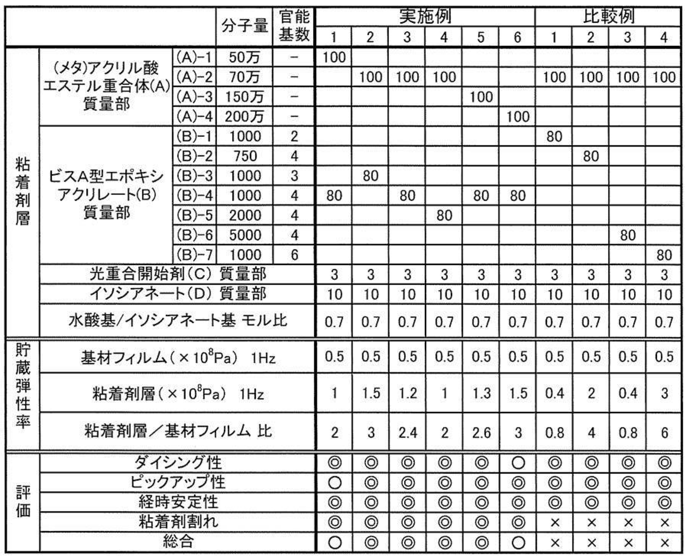
表中に記載した(メタ)アクリル酸エステル重合体(A)、ビスフェノールA型エポキシアクリレート(B)、光重合開始剤(C)、硬化剤(D)には、以下のものを用いた。
(1)(メタ)アクリル酸エステル重合体(A)
(A)-1:重量平均分子量50万の共重合体からなり、溶液重合により得られる市販品(昭和電工社製、製品名ビニロールSPV-8141)。
(A)-2:重量平均分子量70万の共重合体からなり、溶液重合により得られる自社重合品。
(A)-3:重量平均分子量150万の共重合体からなり、溶液重合により得られる自社重合品。
(A)-4:重量平均分子量200万の共重合体からなり、溶液重合により得られる自社重合品。
(A)-1:重量平均分子量50万の共重合体からなり、溶液重合により得られる市販品(昭和電工社製、製品名ビニロールSPV-8141)。
(A)-2:重量平均分子量70万の共重合体からなり、溶液重合により得られる自社重合品。
(A)-3:重量平均分子量150万の共重合体からなり、溶液重合により得られる自社重合品。
(A)-4:重量平均分子量200万の共重合体からなり、溶液重合により得られる自社重合品。
(2)ビスフェノールA型エポキシアクリレート(B)
(B)-1:2官能アクリレートであり、分子量1000の自社重合品。
(B)-2:4官能アクリレートであり、分子量750の自社重合品。
(B)-3:3官能アクリレートであり、分子量1000の自社重合品。
(B)-4:4官能アクリレートであり、分子量1000の市販品(昭和電工社製、製品名リポキシPX-390HT)。
(B)-5:4官能アクリレートであり、分子量2000の自社重合品。
(B)-6:4官能アクリレートであり、分子量5000の自社重合品。
(B)-7:6官能アクリレートであり、分子量1000の自社重合品。
(B)-1:2官能アクリレートであり、分子量1000の自社重合品。
(B)-2:4官能アクリレートであり、分子量750の自社重合品。
(B)-3:3官能アクリレートであり、分子量1000の自社重合品。
(B)-4:4官能アクリレートであり、分子量1000の市販品(昭和電工社製、製品名リポキシPX-390HT)。
(B)-5:4官能アクリレートであり、分子量2000の自社重合品。
(B)-6:4官能アクリレートであり、分子量5000の自社重合品。
(B)-7:6官能アクリレートであり、分子量1000の自社重合品。
(3)光重合開始剤(C)
ベンジルジメチルケタール(チバ・ジャパン社製、製品名Irgacure651)。
ベンジルジメチルケタール(チバ・ジャパン社製、製品名Irgacure651)。
(4)硬化剤(D)
トリレンジイソシアネートのトリメチロールプロパンアダクト体(日本ポリウレタン社製、製品名コロネートL-45E)。粘着剤組成物中の水酸基/イソシアネート基のモル比は以下の式により算出した。
トリレンジイソシアネートのトリメチロールプロパンアダクト体(日本ポリウレタン社製、製品名コロネートL-45E)。粘着剤組成物中の水酸基/イソシアネート基のモル比は以下の式により算出した。

ダミーの回路パターンを形成した直径8インチ×厚さ0.725mmのシリコンウエハに粘着シートを貼合した。ダイシング装置(DISCO社、DAD341)を用いて以下の条件でダイシングを行った。
チップサイズ:3mm×3mm
粘着シートへの切り込み量:45μm
ダイシングブレード:DISCO社、NBC-ZH205O-27HEEE(外径55.56mm、刃幅35μm、内径19.05mm)
ダイシングブレード回転数:40,000rpm
ダイシングブレード送り速度:80mm/秒
切削水温度:25℃
切削水量:1.0L/分
チップサイズ:3mm×3mm
粘着シートへの切り込み量:45μm
ダイシングブレード:DISCO社、NBC-ZH205O-27HEEE(外径55.56mm、刃幅35μm、内径19.05mm)
ダイシングブレード回転数:40,000rpm
ダイシングブレード送り速度:80mm/秒
切削水温度:25℃
切削水量:1.0L/分
粘着シートの基材側から紫外線を照射して粘着剤層を硬化させた。紫外線の照射は、UV照射条件は150mJ/cm2とした。粘着シートをエキスパンド(エキスパンド量8mm)してチップ間隔を広げた後、チップをニードルピンで突き上げ、真空コレットで吸着し、粘着シートとチップとの間で剥離し、チップをピックアップした。ピックアップ装置には、キャノンマシナリー社CAP-300II(ニードルピン形状250μmR、ニードルピン数4、ニードルピン突き上げ高さ0.5mm)を用いた。
作成した粘着シートおよびピックアップ工程について以下の評価を行った。
(1)貯蔵弾性率の測定
「貯蔵弾性率」は、次のようにして測定した。
試験片として長さ20mm、幅3mm、厚み0.03mmのUV照射済みの粘着シートを作製した。UV照射条件は150mJ/cm2とした。貯蔵弾性率の測定は粘弾性計測装置(RSAIII、TAインスツルメント社製)を用い周波数分散(0.01~80Hz)にて測定を行い下記条件の時の貯蔵弾性率を指標とした。
周波数:1Hz
歪み:0.1%
温度:30℃
(1)貯蔵弾性率の測定
「貯蔵弾性率」は、次のようにして測定した。
試験片として長さ20mm、幅3mm、厚み0.03mmのUV照射済みの粘着シートを作製した。UV照射条件は150mJ/cm2とした。貯蔵弾性率の測定は粘弾性計測装置(RSAIII、TAインスツルメント社製)を用い周波数分散(0.01~80Hz)にて測定を行い下記条件の時の貯蔵弾性率を指標とした。
周波数:1Hz
歪み:0.1%
温度:30℃
(2)ダイシング性
ピックアップ工程後のシリコンウエハのダイシングラインを20ライン確認し、ダイシング時に発生するひげの程度を目視で確認し、以下の基準により評価した。
◎(優):ひげがないダイシングラインが10本以上あった。
○(良):ひげがないダイシングラインが5~9本あった。
×(不可):ひげがないダイシングラインが5本未満であった。
ピックアップ工程後のシリコンウエハのダイシングラインを20ライン確認し、ダイシング時に発生するひげの程度を目視で確認し、以下の基準により評価した。
◎(優):ひげがないダイシングラインが10本以上あった。
○(良):ひげがないダイシングラインが5~9本あった。
×(不可):ひげがないダイシングラインが5本未満であった。
(3)ピックアップ性
ピックアップ工程において粘着シートとチップとの間で良好に剥離でき、ダイアタッチフィルムが完全に付着した状態でピックアップできたチップを数え、以下の基準により評価した。
◎(優):95%以上のチップがピックアップできた。
○(良):80%以上95%未満のチップがピックアップできた。
×(不可):80%未満のチップがピックアップできた。
ピックアップ工程において粘着シートとチップとの間で良好に剥離でき、ダイアタッチフィルムが完全に付着した状態でピックアップできたチップを数え、以下の基準により評価した。
◎(優):95%以上のチップがピックアップできた。
○(良):80%以上95%未満のチップがピックアップできた。
×(不可):80%未満のチップがピックアップできた。
(4)粘着剤割れ
ピックアップ工程後の粘着シートのニードルピン突き上げ箇所を顕微鏡で観察し、粘着剤層が割れている箇所の数を計数し、以下の基準により評価した。
◎(優):5%未満の突き上げ箇所で粘着剤割れが発生した。
○(良):5%以上10%未満の突き上げ箇所で粘着剤割れが発生した。
×(不可):10%以上の突き上げ箇所で粘着剤割れが発生した。
ピックアップ工程後の粘着シートのニードルピン突き上げ箇所を顕微鏡で観察し、粘着剤層が割れている箇所の数を計数し、以下の基準により評価した。
◎(優):5%未満の突き上げ箇所で粘着剤割れが発生した。
○(良):5%以上10%未満の突き上げ箇所で粘着剤割れが発生した。
×(不可):10%以上の突き上げ箇所で粘着剤割れが発生した。
(5)経時安定性
粘着シートをシリコンウエハに貼り合わせて、1週間保管後、高圧水銀灯で紫外線を150mJ/cm2照射した後、粘着シートを剥離した。剥離した後のシリコンウエハ表面を観察し、以下の基準により評価した。
◎(優):シリコンウエハ表面に粘着剤が残らない。
○(良):シリコンウエハ表面に粘着剤が残り、その程度が貼り付け面積の5%未満である場合。
×(不可):シリコンウエハ表面に粘着剤が残り、その程度が貼り付け面積の5%以上である場合。
粘着シートをシリコンウエハに貼り合わせて、1週間保管後、高圧水銀灯で紫外線を150mJ/cm2照射した後、粘着シートを剥離した。剥離した後のシリコンウエハ表面を観察し、以下の基準により評価した。
◎(優):シリコンウエハ表面に粘着剤が残らない。
○(良):シリコンウエハ表面に粘着剤が残り、その程度が貼り付け面積の5%未満である場合。
×(不可):シリコンウエハ表面に粘着剤が残り、その程度が貼り付け面積の5%以上である場合。
評価結果を表1に示す。実施例1~6では、ダイシング性、ピックアップ性、粘着剤割れおよび経時安定性のいずれの評価項目においても、優または良の評価が得られた。一方、比較例1~4に係る粘着シートでは粘着剤層の割れの発生が顕著であった。
本発明に係る粘着シートによれば、ピックアップ時のピン突き上げによる粘着剤割れを抑制でき、割れた粘着剤層が半導体部材に付着し、実装時の不良やコンタミの原因となる問題を防止できる。従って、本発明に係る粘着シート、ダイシング後にチップをピックアップし、リードフレーム等にマウントして接着させる電子部品の製造方法に好適に用いられる。
1 粘着シート
2 基材フィルム
3 粘着剤層
4 シリコンウエハまたはパッケージ
41 チップ
5 リングフレーム
6 ダイシングブレード
61 切り込み
7 リードフレーム
2 基材フィルム
3 粘着剤層
4 シリコンウエハまたはパッケージ
41 チップ
5 リングフレーム
6 ダイシングブレード
61 切り込み
7 リードフレーム
Claims (6)
- 基材と、基材の片面に形成された光硬化型の粘着剤層とを備える粘着シートであって、以下の条件で測定した粘着剤層の光硬化後の貯蔵弾性率が0.5~2.0(×108Pa)であり、かつ粘着剤層の光硬化後の貯蔵弾性率/基材の貯蔵弾性率の値が1~3である粘着シート。
周波数:1Hz
歪み:0.1%
温度:30℃ - 前記粘着剤層を形成する粘着剤組成物が、(メタ)アクリル酸エステル重合体(A)、ビスフェノールA型エポキシアクリレート(B)、光重合開始剤(C)、硬化剤(D)を含有してなり、(B)が3~4官能アクリレートで、かつ分子量が1000~2000であり、(D)が3官能以上のイソシアネート基を有するもので、粘着剤組成物中の水酸基/イソシアネート基のモル比の値が0.6~1.2である請求項1に記載の粘着シート。
- (メタ)アクリル酸エステル重合体(A)の重量平均分子量が70万~150万である請求項1又は2記載の粘着シート。
- 前記基材の貯蔵弾性率が0.5~2.0(×108Pa)である請求項1~3の何れか1つに記載の粘着シート。
- 前記粘着剤の光硬化後の貯蔵弾性率が0.5~1.5(×108Pa)である請求項1~4の何れか1つに記載の粘着シート。
- 請求項1~5の何れか1つに記載の粘着シートに電子部品を貼り合わせる貼合工程と、貼合工程後の電子部品のダイシングを行うダイシング工程と、ダイシング工程後、基材の粘着剤層が形成されていない面側から光を照射し、電子部品を粘着剤層からピックアップするピックアップ工程と、を含む電子部品の製造方法。
Priority Applications (1)
| Application Number | Priority Date | Filing Date | Title |
|---|---|---|---|
| JP2013520492A JP5889892B2 (ja) | 2011-06-14 | 2012-05-28 | 粘着シート及び電子部品の製造方法 |
Applications Claiming Priority (2)
| Application Number | Priority Date | Filing Date | Title |
|---|---|---|---|
| JP2011132262 | 2011-06-14 | ||
| JP2011-132262 | 2011-06-14 |
Publications (1)
| Publication Number | Publication Date |
|---|---|
| WO2012172959A1 true WO2012172959A1 (ja) | 2012-12-20 |
Family
ID=47356952
Family Applications (1)
| Application Number | Title | Priority Date | Filing Date |
|---|---|---|---|
| PCT/JP2012/063630 Ceased WO2012172959A1 (ja) | 2011-06-14 | 2012-05-28 | 粘着シート及び電子部品の製造方法 |
Country Status (3)
| Country | Link |
|---|---|
| JP (1) | JP5889892B2 (ja) |
| TW (1) | TW201307509A (ja) |
| WO (1) | WO2012172959A1 (ja) |
Cited By (11)
| Publication number | Priority date | Publication date | Assignee | Title |
|---|---|---|---|---|
| WO2014200071A1 (ja) * | 2013-06-14 | 2014-12-18 | 電気化学工業株式会社 | 粘着シート |
| WO2015178346A1 (ja) * | 2014-05-23 | 2015-11-26 | リンテック株式会社 | 保護膜形成用複合シート |
| WO2015190230A1 (ja) * | 2014-06-10 | 2015-12-17 | リンテック株式会社 | ダイシングシート |
| WO2016080324A1 (ja) * | 2014-11-19 | 2016-05-26 | 住友ベークライト株式会社 | ダイシングフィルム |
| JP2019067996A (ja) * | 2017-10-04 | 2019-04-25 | 日立化成株式会社 | ダイシング用粘着テープ及びダイシングダイボンディング一体型テープ |
| JP2019091903A (ja) * | 2014-03-17 | 2019-06-13 | リンテック株式会社 | ダイシングシートおよび当該ダイシングシートを用いるチップの製造方法 |
| JP2019176114A (ja) * | 2018-03-29 | 2019-10-10 | 住友ベークライト株式会社 | 半導体基板加工用粘着テープ |
| JP2022083953A (ja) * | 2020-11-25 | 2022-06-06 | 住友ベークライト株式会社 | 粘着テープ |
| JP2022083954A (ja) * | 2020-11-25 | 2022-06-06 | 住友ベークライト株式会社 | 粘着テープ |
| JP2023022780A (ja) * | 2021-08-03 | 2023-02-15 | 住友ベークライト株式会社 | 粘着テープ |
| JP2023092116A (ja) * | 2021-12-21 | 2023-07-03 | 東洋インキScホールディングス株式会社 | 加飾シート用粘着剤組成物 |
Citations (4)
| Publication number | Priority date | Publication date | Assignee | Title |
|---|---|---|---|---|
| JP2000044893A (ja) * | 1998-07-31 | 2000-02-15 | Nippon Synthetic Chem Ind Co Ltd:The | 再剥離型粘着剤組成物 |
| JP2010090249A (ja) * | 2008-10-07 | 2010-04-22 | Showa Highpolymer Co Ltd | 紫外線硬化型再剥離性粘着剤組成物及びこれを用いた粘着シート |
| JP2010163518A (ja) * | 2009-01-14 | 2010-07-29 | Denki Kagaku Kogyo Kk | 粘着剤、粘着剤を用いた粘着シート、粘着シートを用いたガラス部品の製造方法 |
| JP2011077235A (ja) * | 2009-09-30 | 2011-04-14 | Nitto Denko Corp | 素子保持用粘着シートおよび素子の製造方法 |
Family Cites Families (1)
| Publication number | Priority date | Publication date | Assignee | Title |
|---|---|---|---|---|
| JP2000090249A (ja) * | 1998-09-14 | 2000-03-31 | Fujitsu Ltd | 画像処理装置および画像処理方法およびコンピュータを画像処理装置として動作させるためのプログラムが記録されたコンピュータ読み取り可能な記録媒体 |
-
2012
- 2012-05-28 JP JP2013520492A patent/JP5889892B2/ja active Active
- 2012-05-28 WO PCT/JP2012/063630 patent/WO2012172959A1/ja not_active Ceased
- 2012-06-08 TW TW101120704A patent/TW201307509A/zh unknown
Patent Citations (4)
| Publication number | Priority date | Publication date | Assignee | Title |
|---|---|---|---|---|
| JP2000044893A (ja) * | 1998-07-31 | 2000-02-15 | Nippon Synthetic Chem Ind Co Ltd:The | 再剥離型粘着剤組成物 |
| JP2010090249A (ja) * | 2008-10-07 | 2010-04-22 | Showa Highpolymer Co Ltd | 紫外線硬化型再剥離性粘着剤組成物及びこれを用いた粘着シート |
| JP2010163518A (ja) * | 2009-01-14 | 2010-07-29 | Denki Kagaku Kogyo Kk | 粘着剤、粘着剤を用いた粘着シート、粘着シートを用いたガラス部品の製造方法 |
| JP2011077235A (ja) * | 2009-09-30 | 2011-04-14 | Nitto Denko Corp | 素子保持用粘着シートおよび素子の製造方法 |
Cited By (27)
| Publication number | Priority date | Publication date | Assignee | Title |
|---|---|---|---|---|
| WO2014200071A1 (ja) * | 2013-06-14 | 2014-12-18 | 電気化学工業株式会社 | 粘着シート |
| JPWO2014200071A1 (ja) * | 2013-06-14 | 2017-02-23 | デンカ株式会社 | 粘着シート |
| JP2019091903A (ja) * | 2014-03-17 | 2019-06-13 | リンテック株式会社 | ダイシングシートおよび当該ダイシングシートを用いるチップの製造方法 |
| JPWO2015178346A1 (ja) * | 2014-05-23 | 2017-04-20 | リンテック株式会社 | 保護膜形成用複合シート |
| WO2015178346A1 (ja) * | 2014-05-23 | 2015-11-26 | リンテック株式会社 | 保護膜形成用複合シート |
| KR102378063B1 (ko) * | 2014-05-23 | 2022-03-23 | 린텍 가부시키가이샤 | 보호막 형성용 복합 시트 |
| CN106463373B (zh) * | 2014-05-23 | 2020-01-03 | 琳得科株式会社 | 保护膜形成用复合片 |
| KR20170008749A (ko) * | 2014-05-23 | 2017-01-24 | 린텍 가부시키가이샤 | 보호막 형성용 복합 시트 |
| CN106463373A (zh) * | 2014-05-23 | 2017-02-22 | 琳得科株式会社 | 保护膜形成用复合片 |
| CN106463375B (zh) * | 2014-06-10 | 2019-06-28 | 琳得科株式会社 | 切割片 |
| JPWO2015190230A1 (ja) * | 2014-06-10 | 2017-04-20 | リンテック株式会社 | ダイシングシート |
| CN106463375A (zh) * | 2014-06-10 | 2017-02-22 | 琳得科株式会社 | 切割片 |
| CN110211912A (zh) * | 2014-06-10 | 2019-09-06 | 琳得科株式会社 | 切割片 |
| CN110211912B (zh) * | 2014-06-10 | 2023-06-02 | 琳得科株式会社 | 切割片 |
| WO2015190230A1 (ja) * | 2014-06-10 | 2015-12-17 | リンテック株式会社 | ダイシングシート |
| WO2016080324A1 (ja) * | 2014-11-19 | 2016-05-26 | 住友ベークライト株式会社 | ダイシングフィルム |
| JP7059553B2 (ja) | 2017-10-04 | 2022-04-26 | 昭和電工マテリアルズ株式会社 | ステルスダイシング用粘着テープ及びダイシングダイボンディング一体型テープ、並びに半導体装置の製造方法 |
| JP2019067996A (ja) * | 2017-10-04 | 2019-04-25 | 日立化成株式会社 | ダイシング用粘着テープ及びダイシングダイボンディング一体型テープ |
| JP2019176114A (ja) * | 2018-03-29 | 2019-10-10 | 住友ベークライト株式会社 | 半導体基板加工用粘着テープ |
| JP7035720B2 (ja) | 2018-03-29 | 2022-03-15 | 住友ベークライト株式会社 | 半導体基板加工用粘着テープ |
| JP2022083953A (ja) * | 2020-11-25 | 2022-06-06 | 住友ベークライト株式会社 | 粘着テープ |
| JP2022083954A (ja) * | 2020-11-25 | 2022-06-06 | 住友ベークライト株式会社 | 粘着テープ |
| JP7099575B2 (ja) | 2020-11-25 | 2022-07-12 | 住友ベークライト株式会社 | 粘着テープ |
| JP7099574B2 (ja) | 2020-11-25 | 2022-07-12 | 住友ベークライト株式会社 | 粘着テープ |
| JP2023022780A (ja) * | 2021-08-03 | 2023-02-15 | 住友ベークライト株式会社 | 粘着テープ |
| JP2023092116A (ja) * | 2021-12-21 | 2023-07-03 | 東洋インキScホールディングス株式会社 | 加飾シート用粘着剤組成物 |
| JP7815743B2 (ja) | 2021-12-21 | 2026-02-18 | artience株式会社 | 加飾シート用粘着剤組成物 |
Also Published As
| Publication number | Publication date |
|---|---|
| JP5889892B2 (ja) | 2016-03-22 |
| JPWO2012172959A1 (ja) | 2015-02-23 |
| TW201307509A (zh) | 2013-02-16 |
Similar Documents
| Publication | Publication Date | Title |
|---|---|---|
| JP5889892B2 (ja) | 粘着シート及び電子部品の製造方法 | |
| JP6604972B2 (ja) | ダイシングテープ | |
| JP6261115B2 (ja) | 粘着シート | |
| US8389629B2 (en) | Adhesive, adhesive sheet, multi-layered adhesive sheet, and production method for electronic part | |
| CN106488963B (zh) | 粘合片、电子部件的制造方法 | |
| JP6031047B2 (ja) | 粘着シートおよび電子部品の製造方法 | |
| JP5460809B1 (ja) | 半導体加工用粘着テープ | |
| KR102359829B1 (ko) | 반도체 검사용의 내열성 점착 시트, 및 반도체 검사 방법 | |
| JP7547499B2 (ja) | 粘着テープ及び加工方法 | |
| JP6782237B2 (ja) | 半導体加工用粘着テープ及びそれを用いた半導体チップ又は半導体部品の製造方法 | |
| JP2004256793A (ja) | ウエハ貼着用粘着テープ | |
| JP5890405B2 (ja) | 粘着シートおよび電子部品の製造方法 | |
| TWI639673B (zh) | 黏著片 | |
| CN113272399A (zh) | 粘合带 |
Legal Events
| Date | Code | Title | Description |
|---|---|---|---|
| 121 | Ep: the epo has been informed by wipo that ep was designated in this application |
Ref document number: 12801348 Country of ref document: EP Kind code of ref document: A1 |
|
| ENP | Entry into the national phase |
Ref document number: 2013520492 Country of ref document: JP Kind code of ref document: A |
|
| NENP | Non-entry into the national phase |
Ref country code: DE |
|
| 122 | Ep: pct application non-entry in european phase |
Ref document number: 12801348 Country of ref document: EP Kind code of ref document: A1 |