WO2012172958A1 - 放射線画像検出装置及び放射線撮影装置 - Google Patents
放射線画像検出装置及び放射線撮影装置 Download PDFInfo
- Publication number
- WO2012172958A1 WO2012172958A1 PCT/JP2012/063610 JP2012063610W WO2012172958A1 WO 2012172958 A1 WO2012172958 A1 WO 2012172958A1 JP 2012063610 W JP2012063610 W JP 2012063610W WO 2012172958 A1 WO2012172958 A1 WO 2012172958A1
- Authority
- WO
- WIPO (PCT)
- Prior art keywords
- image detection
- phosphor
- detection apparatus
- fluorescence
- array
- Prior art date
- Legal status (The legal status is an assumption and is not a legal conclusion. Google has not performed a legal analysis and makes no representation as to the accuracy of the status listed.)
- Ceased
Links
Images




Classifications
-
- G—PHYSICS
- G01—MEASURING; TESTING
- G01T—MEASUREMENT OF NUCLEAR OR X-RADIATION
- G01T1/00—Measuring X-radiation, gamma radiation, corpuscular radiation, or cosmic radiation
- G01T1/29—Measurement performed on radiation beams, e.g. position or section of the beam; Measurement of spatial distribution of radiation
- G01T1/2914—Measurement of spatial distribution of radiation
- G01T1/2985—In depth localisation, e.g. using positron emitters; Tomographic imaging (longitudinal and transverse section imaging; apparatus for radiation diagnosis sequentially in different planes, steroscopic radiation diagnosis)
-
- A—HUMAN NECESSITIES
- A61—MEDICAL OR VETERINARY SCIENCE; HYGIENE
- A61B—DIAGNOSIS; SURGERY; IDENTIFICATION
- A61B6/00—Apparatus or devices for radiation diagnosis; Apparatus or devices for radiation diagnosis combined with radiation therapy equipment
- A61B6/40—Arrangements for generating radiation specially adapted for radiation diagnosis
- A61B6/4035—Arrangements for generating radiation specially adapted for radiation diagnosis the source being combined with a filter or grating
-
- A—HUMAN NECESSITIES
- A61—MEDICAL OR VETERINARY SCIENCE; HYGIENE
- A61B—DIAGNOSIS; SURGERY; IDENTIFICATION
- A61B6/00—Apparatus or devices for radiation diagnosis; Apparatus or devices for radiation diagnosis combined with radiation therapy equipment
- A61B6/42—Arrangements for detecting radiation specially adapted for radiation diagnosis
- A61B6/4208—Arrangements for detecting radiation specially adapted for radiation diagnosis characterised by using a particular type of detector
- A61B6/4233—Arrangements for detecting radiation specially adapted for radiation diagnosis characterised by using a particular type of detector using matrix detectors
-
- A—HUMAN NECESSITIES
- A61—MEDICAL OR VETERINARY SCIENCE; HYGIENE
- A61B—DIAGNOSIS; SURGERY; IDENTIFICATION
- A61B6/00—Apparatus or devices for radiation diagnosis; Apparatus or devices for radiation diagnosis combined with radiation therapy equipment
- A61B6/44—Constructional features of apparatus for radiation diagnosis
- A61B6/4429—Constructional features of apparatus for radiation diagnosis related to the mounting of source units and detector units
- A61B6/4464—Constructional features of apparatus for radiation diagnosis related to the mounting of source units and detector units the source unit or the detector unit being mounted to ceiling
Definitions
- the present invention relates to a radiation image detection apparatus and a radiation imaging apparatus including the radiation image detection apparatus.
- radiological image detection apparatus that detects a radiographic image and generates digital image data has been put into practical use, and is rapidly spreading because it allows an image to be confirmed immediately compared to a conventional imaging plate.
- radiological image detection apparatuses There are various types of radiological image detection apparatuses, and one of them is an indirect conversion type.
- An indirect conversion type radiological image detection apparatus includes a scintillator (phosphor) formed of a fluorescent composition that emits fluorescence by radiation exposure, and an array of pixels that detect the fluorescence generated in the scintillator and convert it into an electrical signal on a substrate. And a provided sensor panel. The radiation transmitted through the subject is converted into light by the scintillator, and the fluorescence of the scintillator is converted into an electrical signal by the pixel of the sensor panel, thereby generating image data.
- a scintillator phosphor
- the radiation transmitted through the subject is converted into light by the scintillator, and the fluorescence of the scintillator is converted into an electrical signal by the pixel of the sensor panel, thereby generating image data.
- image data based on a low energy component of radiation and image data based on a high energy component are acquired, and an image in which a specific structure of a subject (for example, a patient's organ, bone, or blood vessel) is emphasized is obtained.
- An indirect conversion type radiological image detection apparatus for performing so-called energy subtraction is known (see, for example, Patent Document 1).
- the radiological image detection apparatus described in Patent Document 1 includes a sensor panel in which an array of pixels is provided on both sides of a substrate, and two scintillators arranged to face each other with the sensor panel interposed therebetween. ing.
- the low energy component of the radiation transmitted through the subject is absorbed by one scintillator arranged on the radiation incident side, and the fluorescence generated in this scintillator is detected by an array of pixels provided on the substrate surface facing this scintillator. Image data based on the low energy component is acquired.
- the high energy component of radiation passes through the incident side scintillator and the sensor panel and is absorbed by the other scintillator, and the fluorescence generated in this scintillator is an array of pixels provided on the substrate surface facing the scintillator. And image data based on the high energy component is acquired.
- a glass substrate is typically used as the sensor panel substrate.
- the sensor panel substrate is a transparent substrate such as a glass substrate. A part of the fluorescence generated in one scintillator may pass through the substrate without being absorbed by the array of pixels corresponding to the scintillator, and may enter the other array of pixels. Thereby, the contamination of the fluorescence of two scintillators arises and the degradation of an energy subtraction image is caused.
- the present invention has been made in view of the above-described circumstances, and an object of the present invention is to provide a radiation image detection apparatus and a radiation imaging apparatus that can obtain a good energy subtraction image.
- a sensor panel having a substrate having absorption characteristics with respect to light in the first wavelength band, and an array of first pixels and an array of second pixels provided on the substrate, and a first energy
- a first phosphor that emits fluorescence including the first wavelength region by being exposed to radiation in a region, a second energy that is disposed opposite the first phosphor across the sensor panel
- a second phosphor that emits fluorescence when exposed to radiation in the region, wherein the first pixel has spectral sensitivity substantially only in the first wavelength region
- the array comprising: Radiation image detection that is provided on the first phosphor side of the substrate and detects fluorescence generated in the first phosphor, and the second pixel array detects fluorescence generated in the second phosphor. apparatus.
- a sensor panel having a substrate having an absorption characteristic for light in the first wavelength band, and an array of first pixels and an array of second pixels provided on the substrate, and a first energy
- a first phosphor that emits fluorescence contained in the first wavelength range by being exposed to radiation in a region, and is disposed opposite to the first phosphor across the sensor panel;
- a second phosphor that emits fluorescence when exposed to radiation in an energy range, and the first pixel array is provided on the first phosphor side of the substrate, and the first fluorescence
- a radiographic image detection apparatus that detects fluorescence generated in a body, and the second pixel array is provided on the second phosphor side of the substrate to detect fluorescence generated in the second phosphor.
- the radiographic image detection apparatus according to (1) or (2), the first image data acquired by the first pixel array, and the second image data acquired by the second pixel array.
- a radiation imaging apparatus comprising: an image processing unit that generates an energy subtraction image using image data.
- the fluorescence generated in the second phosphor is included in the first wavelength range, or the component in the first wavelength range is included in the fluorescence generated in the second phosphor. They are absorbed by the substrate. Thus, fluorescence contamination is prevented and the image acquired by the first array of pixels depends only on the component of the first energy region of the radiation incident on the radiation image detection device.
- the radiation image detection apparatus of (2) above even if a part of the fluorescence generated in the first phosphor passes through the first pixel array, they are absorbed by the substrate. Therefore, the contamination of the fluorescence is prevented, and the image acquired by the second pixel array depends only on the second energy region component of the radiation incident on the radiation image detection device. As described above, a good energy subtraction image can be obtained.
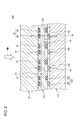
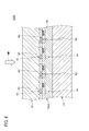
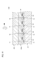
- FIG. 1 It is a figure which shows typically the structure of an example of the radiographic image detection apparatus and radiography apparatus for describing embodiment of this invention. It is a control block diagram of the radiography apparatus of FIG. It is a figure which shows typically the structure of the radiographic image detection apparatus of FIG. It is a figure which shows typically the structure of the modification of the radiographic image detection apparatus of FIG. It is a figure which shows typically the structure of the other modification of the radiographic image detection apparatus of FIG. It is a figure which shows typically the structure of the other example of the radiographic image detection apparatus for describing embodiment of this invention. It is a figure which shows typically the structure of the modification of the radiographic image detection apparatus of FIG. It is a figure which shows typically the structure of the modification of the radiographic image detection apparatus of FIG.
- FIG. 1 shows a configuration of an example of a radiation image detection apparatus and a radiation imaging apparatus for explaining an embodiment of the present invention
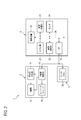
- FIG. 2 shows a control block of the radiation imaging apparatus of FIG.
- An X-ray imaging apparatus 1 shown in FIGS. 1 and 2 is an X-ray diagnostic apparatus that images a subject (patient) H in a standing position, and an X-ray source 2 that emits cone beam X-rays to the subject H;
- An X-ray image detection apparatus 3 that is disposed opposite to the X-ray source 2 and detects X-rays transmitted through the subject H from the X-ray source 2 to generate image data, and the X-ray source 2 based on the operation of the operator It is roughly divided into a console 4 that controls the exposure operation and the imaging operation of the X-ray image detection device 3 and processes image data acquired by the X-ray image detection device 3.
- the X-ray source 2 is held by an X-ray source holding device 5 suspended from the ceiling.
- the X-ray image detection apparatus 3 is held by a stand 6 installed on the floor.
- the X-ray source 2 is emitted from the X-ray tube 12 and the X-ray tube 12 that generates X-rays according to the high voltage applied from the high voltage generator 11 based on the control of the X-ray source control unit 10.
- the X-ray includes a collimator unit 14 having a movable collimator 13 that limits an irradiation field so as to shield a portion that does not contribute to the inspection area of the subject H.
- the X-ray source holding device 5 is connected to a carriage unit 16 configured to be movable in a horizontal direction (z direction) along a ceiling rail 15 installed on the ceiling, and extends downward from the carriage unit 16.
- a plurality of support columns 17, a drive mechanism for moving the carriage unit 16 along the ceiling rail, and a drive mechanism for expanding and contracting the support columns 17 are provided.
- the X-ray source 2 is attached to the distal end portion of the column portion 17.
- the distance SID in the horizontal direction between the X-ray source 2 and the X-ray image detection device 3 is changed, and the support column 17 expands and contracts.
- Both drive mechanisms are controlled by the console 4 based on an operator's setting operation.
- the stand 6 includes a main body 18 installed on the floor, a holding portion 19 attached to the main body 18 so as to be movable in the vertical direction, and a drive mechanism for moving the holding portion 19 up and down.
- the X-ray image detection device 3 is attached to the holding unit 19.
- the drive mechanism is controlled by the console 4 described later based on the setting operation by the operator.
- the console 4 is provided with a control device 20 including a CPU, a ROM, a RAM, and the like.
- the control device 20 includes an input device 21 through which an operator inputs an imaging instruction and the content of the instruction, and an image processing unit 22 that processes the image data acquired by the X-ray image detection device 3 to generate an X-ray image.
- the control device 20, input device 21, image processing unit 22, image storage unit 23, monitor 24, and I / F 25 are connected via a bus 26.
- the distance between the X-ray source 2 and the X-ray image detection device 3 (imaging distance) SID, X-ray imaging conditions such as tube voltage, imaging timing, and the like are input.
- the control device 20 moves the X-ray source 2 to a position corresponding to the input imaging distance SID.
- the radiation source holding device 5 is driven.
- the control device 20 moves the X-ray source 2 to the vertical position facing the X-ray image detection device 3 based on the vertical position of the X-ray image detection device 3 supplied from the stand 6.
- the radiation source holding device 5 is driven.
- the X-ray image detection device 3 includes a sensor panel 30, a first scintillator 31 and a second scintillator 32 that are formed of a fluorescent composition that emits fluorescence by X-ray exposure and is disposed so as to sandwich the sensor panel therebetween. It has.
- the X-ray image detection device 3 is attached to the holding unit 19 so that the first scintillator 31 is positioned on the X-ray source 2 side. X-rays are detected from the X-ray image detection device 3 side from the first scintillator 31 side. Is incident on. X-rays incident on the X-ray image detection device 3 (hereinafter referred to as incident X-rays) first enter the first scintillator 31, and the low energy component is absorbed by the first scintillator 31. On the other hand, the high energy component of incident X-rays is transmitted through the first scintillator 31 and the sensor panel 30 to enter the second scintillator 32 and is absorbed by the second scintillator 32.
- Fluorescence is generated in each of the first scintillator 31 that absorbs the low energy component of the incident X-ray and the second scintillator 32 that absorbs the high energy component, and the fluorescence is individually detected by the sensor panel 30 and is low.
- Two pieces of image data are generated: image data based on energy components and image data based on high energy components. These image data are sent from the sensor panel 30 to the image processing unit 22 (see FIG. 2) of the console 4, and the image processing unit 22 weights both image data appropriately, for example, from one image data to the other.
- An energy subtraction image is generated by subtracting the image data.
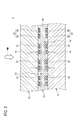
- FIG. 3 shows the configuration of the X-ray image detection apparatus 3.
- the sensor panel 30 includes a substrate 40, and an array of first pixels 41 and an array of second pixels 42 provided on the substrate 40.
- the substrate 40 is formed of a semiconductor material having a band gap of 2.8 eV or more, and has an absorption characteristic for light in a blue (380 nm to 495 nm) wavelength region.
- semiconductor materials include SiC (band gap: 2.8 eV), ZnO (band gap: 3.2 eV), GaN (band gap: 3.4 eV), and the like.
- the array of the first pixels 41 is provided on the surface of the semiconductor substrate 40 facing the first scintillator 31.
- Each of the first pixels 41 receives a fluorescence emitted from the first scintillator 31 and generates a charge, and a photoelectric conversion element 43 such as a photodiode, and reads out the charge generated in the photoelectric conversion element 43.
- a readout circuit unit 44 such as a CCD (Charge-Coupled Device) or a CMOS (Complementary Metal-Oxide-Semiconductor) is formed.
- the photoelectric conversion element 43 and the readout circuit unit 44 are both formed on the semiconductor substrate 40.
- the photoelectric conversion element 43 formed on the semiconductor substrate 40 having absorption characteristics for light in the blue wavelength region has spectral sensitivity substantially only in the blue wavelength region.
- the array of the second pixels 42 is provided on the surface of the semiconductor substrate 40 on the side facing the second scintillator 32.
- Each of the second pixels 42 receives a fluorescence emitted from the second scintillator 32 and generates a charge, and a readout circuit unit 46 for reading out the charge generated in the photoelectric conversion element 45.
- the photoelectric conversion element 45 and the readout circuit unit 46 are both formed on the semiconductor substrate 40. Since the photoelectric conversion element 45 is also formed on the semiconductor substrate 40, the photoelectric conversion element 45 has spectral sensitivity only in a substantially blue wavelength region.
- single crystal Si is typically used for the semiconductor substrate on which the photoelectric conversion element and its readout circuit portion are formed.
- the semiconductor substrate 40 has a band gap of single crystal Si.
- a semiconductor material such as SiC having a band gap greater than 1.1 eV is used, and the X-ray resistance of the photoelectric conversion elements 43 and 45 and the readout circuit portions 44 and 46 formed on the semiconductor substrate 40 is a single crystal Si semiconductor substrate. It is superior to what is formed.
- the photoelectric conversion elements 43 and 45 and the readout circuit units 44 and 46 are excellent in X-ray resistance. preferable.
- the readout circuit portions 44 and 45 such as CCD and CMOS formed on the semiconductor substrate 40 are excellent in terms of readout speed.
- the first scintillator 31 that is arranged on the X-ray incident side of the sensor panel 30 and overlaps the array of the first pixels 41 has a K absorption edge in a relatively low energy region, and mainly uses low energy components of incident X-rays.
- a fluorescent composition that absorbs and emits fluorescence, and has a fluorescence peak wavelength in a blue wavelength range that matches the spectral sensitivity of the first pixel 41 (the photoelectric conversion element 43 included in the pixel 41). Formed by the composition.
- europium activated barium fluorohalide BaFX: Eu (X is a halogen such as Br or I)
- BaFX europium activated barium fluorohalide
- the second scintillator 32 disposed on the opposite side of the first scintillator 31 with the sensor panel 30 interposed therebetween and overlapping the array of the second pixels 42 is a fluorescent composition in which the K absorption end forms the first scintillator 31.
- a fluorescent composition that mainly absorbs high energy components of incident X-rays and emits fluorescence, and the peak wavelength of the fluorescence is the second pixel 42 (included in the pixel 42).
- CaWO 4 calcium tungstate
- incident X-rays first enter the first scintillator 31, and the low energy component is mainly absorbed by the first scintillator 31.
- fluorescence Lb in a blue wavelength region corresponding to the absorbed X-rays is generated, and this fluorescence Lb is detected by the array of the first pixels 41. Thereby, image data based on the low energy component of the incident X-ray is generated.
- the high energy component of the incident X-ray is not absorbed by the first scintillator 31, passes through the first scintillator 31 and the sensor panel 30 and enters the second scintillator 32, and this second scintillator. 32 is absorbed.
- fluorescence Lb in a blue wavelength range corresponding to the absorbed X-rays is generated, and this fluorescence Lb is detected by the array of second pixels 42. Thereby, image data based on the high energy component of incident X-rays is generated.
- the fluorescence Lb generated in the first scintillator 31 and the fluorescence Lb generated in the second scintillator 32 are both in the blue wavelength region, and the first pixel 41 to detect the fluorescence Lb of the first scintillator 31 is used. Is sensitive to the fluorescence Lb of the second scintillator 32 as well.
- a part of the fluorescence Lb generated in the second scintillator 32 is not received by the array of the second pixels 42 and is directed to the array of the first pixels 41 provided on the opposite surface of the semiconductor substrate 40. May go forward.
- the semiconductor substrate 40 has an absorption characteristic with respect to light in the blue wavelength region, and is not received by the array of the second pixels 42 and is directed toward the array of the first pixels 41.
- the fluorescence Lb of the second scintillator 32 that travels is absorbed by the semiconductor substrate 40. Therefore, in the array of the first pixels 41, the fluorescence Lb of the second scintillator 32 is prevented from being detected by being mixed with the fluorescence Lb of the first scintillator 31. Thereby, in the image data based on the low energy component of the incident X-ray, the influence of the high energy component of the incident X-ray is reduced.
- the second pixel 42 that should detect the fluorescence Lb of the second scintillator 32 is sensitive to the fluorescence Lb of the first scintillator 31, but is not received by the array of the first pixels 41.
- the fluorescence Lb of the first scintillator 31 that proceeds toward the array of the second pixels 42 is absorbed by the semiconductor substrate 40. Therefore, in the array of the second pixels 42, the fluorescence Lb of the first scintillator 31 is prevented from being mixed with the fluorescence Lb of the second scintillator 32 and detected. Thereby, in the image data based on the high energy component of the incident X-ray, the influence of the low energy component of the incident X-ray is reduced.
- the contamination of the fluorescence is prevented, and the image data acquired by the array of the first pixels 41 is a component of the low energy region of the incident X-ray.
- the image data acquired by the array of second pixels 42 depends only on the high energy component of the incident X-ray. Thereby, a favorable energy subtraction image can be obtained.
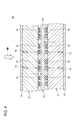
- FIG. 4 shows a modification of the X-ray image detection apparatus 3.
- the reflective layer 33 that reflects the fluorescence Lb generated in the first scintillator 31 is provided on the surface opposite to the side facing the sensor panel 30. Is provided.
- the fluorescence Lb generated in the first scintillator 31 the fluorescence Lb that has traveled to the side opposite to the sensor panel 30 and reached the reflection layer 33 is reflected by the reflection layer 33 toward the sensor panel 30. Thereby, the detection sensitivity in the array of the first pixels 41 is improved.
- a reflective layer 34 that reflects the fluorescence Lb generated in the second scintillator 32 is provided on the surface opposite to the side facing the sensor panel 30. The detection sensitivity in the 42 array is improved.
- the reflective layers 33 and 34 As a material for forming the reflective layers 33 and 34, for example, aluminum or an aluminum alloy can be used.
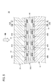
- FIG. 5 shows another modification of the X-ray image detection apparatus 3.
- the X-ray image detection apparatus 3B shown in FIG. 5 includes a sensor panel 30B, and a first scintillator 31 and a second scintillator 32 arranged so as to sandwich the sensor panel therebetween.
- the sensor panel 30B includes a semiconductor substrate 40, and an array of first pixels 41B and an array of second pixels 42B provided on the semiconductor substrate 40.
- the array of the first pixels 41B is provided on the surface of the semiconductor substrate 40 facing the first scintillator 31.
- Each of the first pixels 41B receives a fluorescence emitted from the first scintillator 31, generates a charge, and a readout circuit unit 44 for reading out the charge generated in the photoelectric conversion element 43B.
- the photoelectric conversion element 43B is an organic photoelectric conversion film (hereinafter referred to as a blue absorption OPC (Organic-photoelectric-conversion) film) that selectively absorbs a blue wavelength region and generates charges as a photoelectric conversion film provided between a pair of electrodes. ), And is formed on the semiconductor substrate 40.
- the array of the second pixels 42B is provided on the surface of the semiconductor substrate 40 on the side facing the second scintillator 32.
- Each of the second pixels 42B receives a fluorescence emitted from the second scintillator 32 and generates a charge, and a readout circuit unit 46 for reading out the charge generated in the photoelectric conversion element 45B. It consists of and.
- the photoelectric conversion element 45 ⁇ / b> B is an organic photoelectric conversion element using a blue absorption OPC film as a photoelectric conversion film provided between a pair of electrodes, and is formed on the semiconductor substrate 40.
- the photoelectric conversion elements 43B and 45B have a spectral sensitivity substantially only in the blue wavelength range.
- the photoelectric conversion element using the OPC film hardly absorbs X-rays, and therefore has excellent X-ray resistance and absorbs X-rays. The generated noise is suppressed.
- an OPC film described in JP-A-2009-218599 can be used.
- FIG. 6 shows another example of a radiological image detection apparatus for explaining an embodiment of the present invention.
- description is abbreviate
- the radiation image detection apparatus 103 is arranged so that X-rays enter from the first scintillator 31 side.
- the sensor panel 130 includes a semiconductor substrate 40 that has absorption characteristics with respect to light in a blue wavelength range, and an array of first pixels 41 and an array of second pixels 142 provided on the semiconductor substrate 40. .
- the array of the first pixels 41 is provided on the surface of the 40th semiconductor substrate facing the first scintillator 31.
- Each of the first pixels 41 has spectral sensitivity substantially only in the blue wavelength region.
- the second pixels 142 are provided on the surface of the semiconductor substrate 40 facing the second scintillator 132, and each of the second pixels 142 receives fluorescence emitted from the second scintillator 132.
- the first scintillator 31 is a fluorescent composition that has a K absorption edge in a relatively low energy range, mainly absorbs a low energy component of incident X-rays, and emits fluorescence, and has a peak wavelength of fluorescence.
- it is formed of a fluorescent composition such as BaFX: Eu in the blue wavelength range that matches the spectral sensitivity of one pixel 41 (the photoelectric conversion element 43 included in the pixel 41).
- the second scintillator 132 is a fluorescent composition whose K absorption edge is in a higher energy region than the fluorescent composition forming the first scintillator 31 and emits fluorescence mainly by absorbing high energy components of incident X-rays. And a fluorescent composition that emits fluorescence having a peak wavelength in a green wavelength range (495 nm to 570 nm) that deviates from the blue wavelength range. Examples of such a fluorescent composition include terbium-activated gadolinium oxide (Gd 2 O 2 S: Tb).
- the second pixel 142 has spectral sensitivity in the green wavelength region where the main peak wavelength of the fluorescence generated in the second scintillator 132 is, the second pixel 142 is spectrally separated into another wavelength region (for example, the blue wavelength region). Although it may have sensitivity, in the X-ray image detection apparatus 103 of this example, the photoelectric conversion element 145 included in the second pixel 142 has a green wavelength as a photoelectric conversion film provided between the pair of electrodes.
- An organic photoelectric conversion element using an OPC film hereinafter referred to as a green absorption OPC film that selectively absorbs a region to generate a charge and has a spectral sensitivity only in a substantially green wavelength region. Yes.
- an OPC film using quinacridone described in JP-A-2009-32854 can be used.
- incident X-rays first enter the first scintillator 31, and the low energy component is mainly absorbed by the first scintillator 31.
- fluorescence Lb in a blue wavelength region corresponding to the absorbed X-rays is generated, and this fluorescence Lb is detected by the array of the first pixels 41. Thereby, image data based on the low energy component of the incident X-ray is generated.
- the high energy component of the incident X-rays is not absorbed by the first scintillator 31, passes through the first scintillator 31 and the sensor panel 130, and enters the second scintillator 132, and this second scintillator Absorbed by 132.
- fluorescence Lg in the green wavelength region corresponding to the absorbed X-rays is generated, and this fluorescence Lg is detected by the array of second pixels 142. Thereby, image data based on the high energy component of incident X-rays is generated.
- the peak wavelength of the fluorescence Lg generated in the second scintillator 132 is in the green wavelength range that is out of the blue wavelength range where the spectral sensitivity of the first pixel 41 is, and a part of the fluorescence Lg is the second wavelength. Even if the light reaches the array of the first pixels 41 without being received by the array of the pixels 142, it is not detected by the array of the first pixels 41.
- Gd 2 O 2 S: Tb is used for the fluorescent composition forming the second scintillator 132, the fluorescence generated in the second scintillator 132 includes a little fluorescence Lb in the blue wavelength region.
- the fluorescence Lb is absorbed by the semiconductor substrate 40 having an absorption characteristic with respect to light in the blue wavelength region, and therefore is not detected by the array of the first pixels 41. Therefore, in the array of the first pixels 41, the fluorescence of the second scintillator 32 is prevented from being mixed with the fluorescence of the first scintillator 31 and detected.
- the second pixel 142 has a spectral sensitivity substantially only in the green wavelength region and does not have a spectral sensitivity in the blue wavelength region.
- the fluorescence Lb in the blue wavelength region that occurs in the first scintillator 31 is larger than the fluorescence Lb in the blue wavelength region that occurs in the second scintillator 132, and tentatively, part of the fluorescence Lb that occurs in the first scintillator 31 Is detected by the array of second pixels 142 even if it reaches the array of second pixels 142 without being received by the array of first pixels 41 and not sufficiently absorbed by the semiconductor substrate 40. None happen. Therefore, in the array of the second pixels 142, the fluorescence Lb of the first scintillator 31 is prevented from being detected by being mixed with the fluorescence Lg of the second scintillator 132.
- FIG. 7 shows a modification of the X-ray image detection apparatus 103.
- the 7 includes a sensor panel 130A, and a first scintillator 31 and a second scintillator 132 disposed so as to sandwich the sensor panel 130A.
- the sensor panel 130 ⁇ / b> A includes a semiconductor substrate 40, and an array of first pixels 141 and an array of second pixels 142 provided on the semiconductor substrate 40.
- the array of the first pixels 141 is provided on the surface of the semiconductor substrate 40 facing the first scintillator 31.
- the photoelectric conversion element 143 included in each of the first pixels 141 is an organic photoelectric conversion element in which a blue absorption OPC film is used as a photoelectric conversion film provided between a pair of electrodes, and has a substantially blue wavelength range. Only has a spectral sensitivity, and is formed on the semiconductor substrate 40. Note that the readout circuit portion 44 included in the first pixel 141 is formed on the semiconductor substrate 40.
- the first pixels 41 and 141 have been described as having spectral sensitivity only in the substantially blue wavelength range. However, in these X-ray image detection apparatuses, The first pixel may have spectral sensitivity even in a wavelength region outside of blue.
- the fluorescence Lb of the first scintillator 31 is included in the blue wavelength region absorbed by the semiconductor substrate 40, and the array of the second pixels 142 is provided in the semiconductor substrate 40. It is provided on the opposite side to the side. In such a configuration, a part of the fluorescence Lg in the green wavelength region of the second scintillator 132 is not received by the array of the second pixels 142 and passes through the semiconductor substrate 40 and reaches the array of the first pixels. In this case, if the first pixel also has spectral sensitivity in the green wavelength range, this fluorescence Lg is also detected by the first pixel array. That is, the image data generated by the first array of pixels is based on the low energy component and the high energy component of the incident X-ray.
- the image acquired by the array of second pixels 142 is based on the high energy component of incident X-rays.
- the image data generated by the array of the second pixels 142 is based on one energy component (in this example, a high energy component) of incident X-rays, an energy subtraction image is generated. There is no hindrance.
- the fluorescence of the first scintillator 31 is included in the blue wavelength range absorbed by the semiconductor substrate 40, and the array of the second pixels 42, 42B. Is provided on the opposite side of the semiconductor substrate 40 from the side on which the array of the first pixels 41 and 41B is provided. Also in these X-ray image detection devices, the first pixel is provided on the semiconductor substrate 40. It is not limited to one having spectral sensitivity only in the blue wavelength region having absorption characteristics.
- FIG. 8 shows a modification of the X-ray image detection apparatus 103A.
- the array of the first pixels 141 and the array of the second pixels 142 provided on the sensor panel 130B are both on the side facing the first scintillator 31 in the semiconductor substrate 40.
- the organic photoelectric conversion element 143 (see FIG. 7) included in the first pixel 141 and the organic photoelectric conversion element 145 (see FIG. 6) included in the second pixel 142 are provided on the semiconductor substrate 40. It is formed on top and constitutes a single layer. Thereby, the thickness of the X-ray image detection apparatus can be reduced as compared with the case where an array of photoelectric conversion elements is provided on each of both surfaces of the semiconductor substrate 40.
- the first pixel 141 and the second pixel 142 are each arranged in a double column, and the column of the first pixel 141 and the column of the second pixel 142 are alternately arranged.
- the first pixels 141 and the second pixels 142 are arranged in a staggered manner, and the second pixels 142 are arranged between two adjacent first pixels 141 in each row and each column. Also good.
- incident X-rays first enter the first scintillator 31, and the low energy components are mainly absorbed by the first scintillator 31.
- fluorescence Lb in a blue wavelength region corresponding to the absorbed X-rays is generated, and this fluorescence Lb is detected by the array of the first pixels 141. Thereby, image data based on the low energy component of the incident X-ray is generated.
- the high energy component of the incident X-ray is not absorbed by the first scintillator 31, passes through the first scintillator 31 and the sensor panel 130B, enters the second scintillator 132, and this second scintillator. Absorbed by 132.
- fluorescence Lg in the green wavelength region corresponding to the absorbed X-rays is generated, and this fluorescence Lg passes through the semiconductor substrate 40 and is detected by the array of the second pixels 142. Thereby, image data based on the high energy component of incident X-rays is generated.
- the above-described X-ray image detection apparatuses 3 and 103 and modifications thereof mainly utilize the difference in K absorption edge between the fluorescent composition forming the first scintillator and the fluorescent composition forming the second scintillator.
- the low energy component and the high energy component of incident X-rays are separated, the low X-ray intensity of incident X-rays is determined by utilizing the difference in transmittance due to the energy of X-rays regardless of the K absorption edge of the fluorescent composition.
- the energy component and the high energy component can also be separated and will be described below.
- FIG. 9 shows another example of the radiation image detection apparatus for explaining the embodiment of the present invention. Note that elements common to the above-described X-ray image detection apparatuses 3 and 103 and modifications thereof are denoted by the same reference numerals, and description thereof is omitted or simplified.
- the radiation image detection apparatus 203 is arranged so that X-rays enter from the first scintillator 231 side.
- the sensor panel 230 includes a semiconductor substrate 40 having absorption characteristics with respect to light in a blue wavelength region, and an array of first pixels 41 and an array of second pixels 142 provided on the semiconductor substrate 40. .
- the array of the first pixels 41 is provided on the surface of the 40th semiconductor substrate facing the first scintillator 231.
- the photoelectric conversion element and the readout circuit portion included in each of the first pixels 41 are both formed on the semiconductor substrate 40, and the first pixel 41 has a spectral sensitivity substantially only in the blue wavelength region. is doing.
- the array of the second pixels 142 is provided on the surface of the semiconductor substrate 40 facing the second scintillator 232.
- the photoelectric conversion element included in each of the second pixels 142 is an organic photoelectric conversion element in which a green absorption OPC film is used as a photoelectric conversion film provided between a pair of electrodes, and has a substantially green wavelength range. Only has a spectral sensitivity, and is formed on the semiconductor substrate 40. Note that a reading circuit portion included in the second pixel 142 is formed on the semiconductor substrate 40.
- the first scintillator 231 and the second scintillator 232 are both formed of a mixture of the first fluorescent composition and the second fluorescent composition.
- the first fluorescent composition is, for example, BaFX: Eu or the like, in which the peak wavelength of fluorescence is in a blue wavelength range that matches the spectral sensitivity of the first pixel 41.
- the second fluorescent composition is, for example, Gd 2 O 2 S: Tb or the like, in which the peak wavelength of fluorescence is in the green wavelength range that is out of the blue wavelength range.
- incident X-rays first enter the first scintillator 231.
- the low energy component of the incident X-ray is inferior to the high energy component, and most of it is absorbed by the first scintillator 231.
- the first scintillator 231 has, in accordance with the absorbed X-rays, fluorescence Lb in the blue wavelength range resulting from the first fluorescent composition and fluorescence Lg in the green wavelength range resulting from the second fluorescent composition. Arise.
- fluorescence Lb in the blue wavelength region caused by the first fluorescent composition is detected by the array of the first pixels 41. Thereby, image data based on the low energy component of the incident X-ray is generated.
- the high energy component of the incident X-ray is not absorbed by the first scintillator 231 because of its high transparency, and passes through the first scintillator 231 and the sensor panel 230 to enter the second scintillator 232.
- Incident light is absorbed by the second scintillator 232.
- the second scintillator 232 has, in accordance with the absorbed X-rays, the fluorescence Lb in the blue wavelength range caused by the first fluorescence composition and the fluorescence Lg in the green wavelength range caused by the second fluorescence composition. Arise.
- the fluorescence Lb in the blue wavelength region in which the first pixel 41 has spectral sensitivity is absorbed by the semiconductor substrate 40 having absorption characteristics with respect to the light in the blue wavelength region. It is not detected by the array of pixels 41. Therefore, in the array of the first pixels 41, the fluorescence of the second scintillator 232 is prevented from being mixed with the fluorescence of the first scintillator 231 and detected.
- the fluorescence Lg in the green wavelength region caused by the second fluorescent composition generated in the first scintillator 231 reaches the array of the second pixels 142 through the semiconductor substrate 40, and this fluorescence Lg Is also detected by an array of second pixels 142. That is, the image data generated by the array of the second pixels 142 is based on the high energy component and low energy component of the incident X-ray. However, since the image data generated by the array of the first pixels 41 is based on one energy component (low energy component in this example) of the incident X-ray, there is no problem in generating the energy subtraction image. Absent.
- the apparatus configuration can be simplified, and the thickness of the scintillator (the first scintillator 231 in this example) disposed on the X-ray incident side can be reduced.
- FIG. 10 shows a modification of the X-ray image detection apparatus 203.
- the X-ray image detection apparatus 203A shown in FIG. 10 includes a sensor panel 230A, and a first scintillator 231 and a second scintillator 232 arranged so as to sandwich the sensor panel 230A.
- the sensor panel 230 ⁇ / b> A includes a semiconductor substrate 40, and an array of first pixels 141 and an array of second pixels 142 provided on the semiconductor substrate 40.
- the array of the first pixels 141 is provided on the surface of the semiconductor substrate 40 on the side facing the first scintillator 231.
- the photoelectric conversion element included in each of the first pixels 141 is an organic photoelectric conversion element in which a blue absorption OPC film is used as a photoelectric conversion film provided between a pair of electrodes, and has a substantially blue wavelength range. Only has a spectral sensitivity and is formed on the semiconductor substrate 40.
- FIG. 11 shows a modification of the X-ray image detection apparatus 203A.
- the array of the first pixels 141 and the array of the second pixels 142 provided on the sensor panel 230B are both on the side facing the first scintillator 231 on the semiconductor substrate 40.
- the organic photoelectric conversion element included in the first pixel 141 and the organic photoelectric conversion element included in the second pixel 142 are formed on the semiconductor substrate 40 and constitute a single layer. ing.
- the X-ray image detection device 203B is arranged so that X-rays enter from the second scintillator 232 side.
- incident X-rays first enter the second scintillator 232. Most of the low energy component of the incident X-ray is absorbed by the second scintillator 232.
- the second scintillator 232 has, in accordance with the absorbed X-rays, the fluorescence Lb in the blue wavelength range caused by the first fluorescence composition and the fluorescence Lg in the green wavelength range caused by the second fluorescence composition. Arise.
- the fluorescence Lb in the blue wavelength region resulting from the first fluorescent composition is absorbed by the semiconductor substrate 40.
- the fluorescent light Lg in the green wavelength region caused by the second fluorescent composition reaches the array of the first pixels 141 and the array of the second pixels 142 without being absorbed by the semiconductor substrate 40.
- the high energy component of the incident X-ray is transmitted through the second scintillator 232 and the sensor panel 230, enters the first scintillator 231, and is absorbed by the first scintillator 231.
- the fluorescence Lb in the blue wavelength range caused by the first fluorescence composition and the fluorescence Lg in the green wavelength range caused by the second fluorescence composition depend on the absorbed X-rays. Arise.
- the fluorescence Lb is detected by the first pixel 141 having spectral sensitivity only in the blue wavelength region. Thereby, image data based on the high energy component of incident X-rays is generated.
- the fluorescence Lg in the green wavelength region caused by the second fluorescent composition generated in the first scintillator 231 reaches the array of the second pixels 142 through the semiconductor substrate 40, and this fluorescence Lg Is also detected by an array of second pixels 142. That is, the image data generated by the array of the second pixels 142 is based on the high energy component and low energy component of the incident X-ray. However, since the image data generated by the array of the first pixels 141 is based on one energy component (high energy component in this example) of the incident X-ray, there is no problem in generating the energy subtraction image. Absent.
- the above-described radiographic image detection apparatus can detect a radiographic image with high sensitivity and high definition, and is therefore required to detect a sharp image with a low radiation dose, such as an X-ray imaging apparatus for medical diagnosis such as mammography. It can be used by incorporating it into various devices. For example, it can be used for nondestructive inspection as an industrial X-ray imaging apparatus, or can be used as a detection apparatus for particle beams ( ⁇ rays, ⁇ rays, ⁇ rays) other than electromagnetic waves, and its application range is wide. .
Landscapes
- Physics & Mathematics (AREA)
- Health & Medical Sciences (AREA)
- Life Sciences & Earth Sciences (AREA)
- General Physics & Mathematics (AREA)
- High Energy & Nuclear Physics (AREA)
- Molecular Biology (AREA)
- Spectroscopy & Molecular Physics (AREA)
- Measurement Of Radiation (AREA)
- Radiography Using Non-Light Waves (AREA)
- Apparatus For Radiation Diagnosis (AREA)
Abstract
放射線画像検出装置3は、第1の波長域の光に対して吸収特性を有する基板40と第1の画素41のアレイ及び第2の画素42のアレイとを有するセンサパネル30と、第1のエネルギー域の放射線に露光されることによって第1の波長域を含む蛍光を発する第1の蛍光体31と、センサパネルを挟んで第1の蛍光体と対向して配置され、第2のエネルギー域の放射線に露光されることによって蛍光を発する第2の蛍光体32と、を備え、第1の画素は、実質的に第1の波長域にのみ分光感度を有し、そのアレイは第1の蛍光体側に設けられ、第1の蛍光体に生じる蛍光を検出し、第2の画素のアレイは第2の蛍光体に生じる蛍光を検出する。
Description
本発明は、放射線画像検出装置、及び該放射線画像検出装置を備えた放射線撮影装置に関する。
近年、放射線像を検出してデジタル画像データを生成する放射線画像検出装置が実用化されており、従来のイメージングプレートに比べて即時に画像を確認できるといった理由から急速に普及が進んでいる。この放射線画像検出装置には種々の方式のものがあり、その一つとして、間接変換方式のものが知られている。
間接変換方式の放射線画像検出装置は、放射線露光によって蛍光を発する蛍光組成物によって形成されたシンチレータ(蛍光体)と、シンチレータに生じた蛍光を検出して電気信号に変換する画素のアレイが基板に設けられたセンサパネルとを備えている。被写体を透過した放射線は、シンチレータによって光に変換され、シンチレータの蛍光は、センサパネルの画素によって電気信号に変換され、それにより画像データが生成される。
そして、放射線の低エネルギー成分に基づく画像データと、高エネルギー成分に基づく画像データとを取得して、被写体の特定の構造物(例えば、患者の臓器、骨部又は血管)が強調された画像を生成する、所謂エネルギーサブトラクションを行うための間接変換方式の放射線画像検出装置が知られている(例えば、特許文献1参照)。
特許文献1に記載された放射線画像検出装置は、基板の両面に画素のアレイがそれぞれ設けられたセンサパネルと、このセンサパネルを間に挟んで対向して配置される2つのシンチレータとで構成されている。被写体を透過した放射線の低エネルギー成分は、放射線入射側に配置される一方のシンチレータによって吸収され、このシンチレータに生じた蛍光が、このシンチレータに対向する基板面に設けられた画素のアレイによって検出され、低エネルギー成分に基づく画像データが取得される。また、放射線の高エネルギー成分は、入射側のシンチレータを及びセンサパネルを透過して他方のシンチレータによって吸収され、このシンチレータに生じた蛍光が、このシンチレータに対向する基板面に設けられた画素のアレイによって検出され、高エネルギー成分に基づく画像データが取得される。
センサパネルの基板には、典型的には、ガラス基板が用いられる。特許文献1に記載された放射線画像検出装置のように、センサパネルが2つのシンチレータによって挟まれて構成された放射線画像検出装置において、センサパネルの基板が、ガラス基板等の透明基板であると、一方のシンチレータに生じた蛍光の一部が、そのシンチレータに対応する画素のアレイによって吸収されずに基板を透過し、他方の画素のアレイに入射する場合がある。それによって、2つのシンチレータの蛍光のコンタミネーションが生じ、エネルギーサブトラクション画像の劣化を招く。
本発明は、上述した事情に鑑みなされたものであり、良好なエネルギーサブトラクション画像を得ることができる放射線画像検出装置及び放射線撮影装置を提供することを目的とする。
(1) 第1の波長域の光に対して吸収特性を有する基板と、前記基板に設けられる第1の画素のアレイ及び第2の画素のアレイと、を有するセンサパネルと、第1のエネルギー域の放射線に露光されることによって前記第1の波長域を含む蛍光を発する第1の蛍光体と、前記センサパネルを挟んで前記第1の蛍光体と対向して配置され、第2のエネルギー域の放射線に露光されることによって蛍光を発する第2の蛍光体と、を備え、前記第1の画素は、実質的に前記第1の波長域にのみ分光感度を有し、そのアレイは、前記基板における前記第1の蛍光体側に設けられ、前記第1の蛍光体に生じる蛍光を検出し、前記第2の画素のアレイは、前記第2の蛍光体に生じる蛍光を検出する放射線画像検出装置。
(2) 第1の波長域の光に対して吸収特性を有する基板と、前記基板に設けられる第1の画素のアレイ及び第2の画素のアレイと、を有するセンサパネルと、第1のエネルギー域の放射線に露光されることによって前記第1の波長域に含まれる蛍光を発する第1の蛍光体と、前記センサパネルを挟んで前記第1の蛍光体と対向して配置され、第2のエネルギー域の放射線に露光されることによって蛍光を発する第2の蛍光体と、を備え、前記第1の画素のアレイは、前記基板における前記第1の蛍光体側に設けられ、前記第1の蛍光体に生じる蛍光を検出し、前記第2の画素のアレイは、前記基板における前記第2の蛍光体側に設けられ、前記第2の蛍光体に生じる蛍光を検出する放射線画像検出装置。
(3) 上記(1)又は(2)の放射線画像検出装置と、前記第1の画素のアレイによって取得される第1の画像データ、及び前記第2の画素のアレイによって取得される第2の画像データを用いて、エネルギーサブトラクション画像を生成する画像処理部と、を備える放射線撮影装置。
(2) 第1の波長域の光に対して吸収特性を有する基板と、前記基板に設けられる第1の画素のアレイ及び第2の画素のアレイと、を有するセンサパネルと、第1のエネルギー域の放射線に露光されることによって前記第1の波長域に含まれる蛍光を発する第1の蛍光体と、前記センサパネルを挟んで前記第1の蛍光体と対向して配置され、第2のエネルギー域の放射線に露光されることによって蛍光を発する第2の蛍光体と、を備え、前記第1の画素のアレイは、前記基板における前記第1の蛍光体側に設けられ、前記第1の蛍光体に生じる蛍光を検出し、前記第2の画素のアレイは、前記基板における前記第2の蛍光体側に設けられ、前記第2の蛍光体に生じる蛍光を検出する放射線画像検出装置。
(3) 上記(1)又は(2)の放射線画像検出装置と、前記第1の画素のアレイによって取得される第1の画像データ、及び前記第2の画素のアレイによって取得される第2の画像データを用いて、エネルギーサブトラクション画像を生成する画像処理部と、を備える放射線撮影装置。
上記(1)の放射線画像検出装置によれば、第2の蛍光体に生じる蛍光が第1の波長域に含まれ、若しくは第2の蛍光体に生じる蛍光に第1の波長域の成分が含まれていても、それらは基板によって吸収される。よって、蛍光のコンタミネーションが防止され、第1の画素のアレイによって取得される画像は、放射線画像検出装置に入射する放射線の第1のエネルギー域の成分にのみ依存する。また、上記(2)の放射線画像検出装置によれば、第1の蛍光体に生じる蛍光の一部が、第1の画素のアレイを通過しても、それらは基板によって吸収される。よって、蛍光のコンタミネーションが防止され、第2の画素アレイによって取得される画像は、放射線画像検出装置に入射する放射線の第2のエネルギー域の成分にのみ依存する。以上により、良好なエネルギーサブトラクション画像を得ることができる。
図1は、本発明の実施形態を説明するための、放射線画像検出装置及び放射線撮影装置の一例の構成を示し、図2は、図1の放射線撮影装置の制御ブロックを示す。
図1及び図2に示すX線撮影装置1は、被写体(患者)Hを立位状態で撮影するX線診断装置であって、被写体HにコーンビームX線を放射するX線源2と、X線源2に対向配置されてX線源2から被写体Hを透過したX線を検出して画像データを生成するX線画像検出装置3と、操作者の操作に基づいてX線源2の曝射動作やX線画像検出装置3の撮影動作を制御するとともに、X線画像検出装置3により取得された画像データを処理するコンソール4とに大別される。X線源2は、天井から吊り下げられたX線源保持装置5により保持されている。X線画像検出装置3は、床に設置されたスタンド6により保持されている。
X線源2は、X線源制御部10の制御に基づき、高電圧発生器11から印加される高電圧に応じてX線を発生するX線管12と、X線管12から発せられたX線のうち、被写体Hの検査領域に寄与しない部分を遮蔽するように照射野を制限する可動式のコリメータ13を有するコリメータユニット14とから構成されている。
X線源保持装置5は、天井に設置された天井レール15に沿って水平方向(z方向)に移動自在に構成された台車部16と、互いに連結されて台車部16から下方向に延伸する複数の支柱部17と、台車部16を天井レールに沿って移動させるための駆動機構及び支柱部17を伸縮させるための駆動機構とを備えている。X線源2は、支柱部17の先端部に取り付けられている。X線源保持装置5が天井レール15に沿って移動することにより、X線源2とX線画像検出装置3との間の水平方向に関する距離SIDが変更され、また、支柱部17が伸縮することによって、X線源2の上下方向に関する位置が変更される。両駆動機構は、操作者の設定操作に基づき、コンソール4により制御される。
スタンド6は、床に設置された本体18と、本体18に上下方向に移動自在に取り付けられた保持部19と、保持部19を上下移動させるための駆動機構を備えている。X線画像検出装置3は、保持部19に取り付けられている。駆動機構は、操作者の設定操作に基づき、後述するコンソール4により制御される。
コンソール4には、CPU、ROM、RAM等からなる制御装置20が設けられている。
制御装置20には、操作者が撮影指示やその指示内容を入力する入力装置21と、X線画像検出装置3により取得された画像データを処理してX線画像を生成する画像処理部22と、X線画像を記憶する画像記憶部23と、X線画像等を表示するモニタ24と、X線撮影装置1の各部と接続されるインターフェース(I/F)25とを備えている。制御装置20、入力装置21、画像処理部22、画像記憶部23、モニタ24、及びI/F25は、バス26を介して接続されている。
制御装置20には、操作者が撮影指示やその指示内容を入力する入力装置21と、X線画像検出装置3により取得された画像データを処理してX線画像を生成する画像処理部22と、X線画像を記憶する画像記憶部23と、X線画像等を表示するモニタ24と、X線撮影装置1の各部と接続されるインターフェース(I/F)25とを備えている。制御装置20、入力装置21、画像処理部22、画像記憶部23、モニタ24、及びI/F25は、バス26を介して接続されている。
入力装置21の操作により、X線源2-X線画像検出装置3間距離(撮影距離)SIDや管電圧等のX線撮影条件、撮影タイミング等が入力される。制御装置20は、X線源保持装置5から供給されるX線源2の水平方向位置に基づいて、上記の入力された撮影距離SIDとなる位置にX線源2を移動させるように、X線源保持装置5を駆動する。また、制御装置20は、スタンド6から供給されるX線画像検出装置3の上下方向位置に基づいて、X線画像検出装置3に対向する上下方向位置にX線源2を移動させるようにX線源保持装置5を駆動する。
X線画像検出装置3は、センサパネル30と、X線露光によって蛍光を発する蛍光組成物によって形成され、センサパネルを間に挟むように配置された第1のシンチレータ31及び第2のシンチレータ32とを備えている。
X線画像検出装置3は、第1のシンチレータ31がX線源2側に位置するように保持部19に取り付けられており、X線は、第1のシンチレータ31側からX線画像検出装置3に入射する。X線画像検出装置3に入射したX線(以下、入射X線という)は、まず、第1のシンチレータ31に入射し、その低エネルギー成分が、第1のシンチレータ31によって吸収される。一方、入射X線の高エネルギー成分は、第1のシンチレータ31及びセンサパネル30を透過して第2のシンチレータ32に入射し、第2のシンチレータ32によって吸収される。
入射X線の低エネルギー成分を吸収した第1のシンチレータ31、及び高エネルギー成分を吸収した第2のシンチレータ32の各々において蛍光が生じ、それらの蛍光は、センサパネル30によって個別に検出され、低エネルギー成分に基づく画像データ及び高エネルギー成分に基づく画像データの2つの画像データが生成される。これらの画像データは、センサパネル30からコンソール4の画像処理部22(図2参照)に送出され、画像処理部22は、例えば両画像データに適宜な重み付けを行い、一方の画像データから他方の画像データを減算することによって、エネルギーサブトラクション画像を生成する。
図3は、X線画像検出装置3の構成を示す。
まず、X線画像検出装置3のセンサパネル30について説明する。
センサパネル30は、基板40と、基板40に設けられた第1の画素41のアレイ及び第2の画素42のアレイと、を有する。
基板40は、バンドギャップが2.8eV以上の半導体材料によって形成されており、青色(380nm~495nm)の波長域の光に対して吸収特性を有する。そのような半導体材料としては、SiC(バンドギャップ:2.8eV)、ZnO(バンドギャップ:3.2eV)、GaN(バンドギャップ:3.4eV)、等を例示することができる。
第1の画素41のアレイは、半導体基板40において第1のシンチレータ31に対向する側の面に設けられている。第1の画素41の各々は、第1のシンチレータ31から出射される蛍光を受光して電荷を生成するフォトダイオードなどの光電変換素子43と、光電変換素子43において生成された電荷を読み出すためのCCD(Charge Coupled Device)やCMOS(Complementary Metal Oxide Semiconductor)などの読み出し回路部44とで構成されており、光電変換素子43及び読み出し回路部44は、いずれも半導体基板40に形成されている。このように、青色の波長域の光に対する吸収特性を有する半導体基板40に形成された光電変換素子43は、実質的に青色の波長域にのみ分光感度を有する。
第2の画素42のアレイは、半導体基板40において第2のシンチレータ32に対向する側の面に設けられている。第2の画素42の各々は、第2のシンチレータ32から出射される蛍光を受光して電荷を生成する光電変換素子45と、光電変換素子45において生成された電荷を読み出すための読み出し回路部46とで構成されており、光電変換素子45及び読み出し回路部46は、いずれも半導体基板40に形成されている。光電変換素子45もまた、半導体基板40に形成されることにより、実質的に青色の波長域にのみ分光感度を有する。
なお、光電変換素子やその読み出し回路部が形成される半導体基板には、典型的には、単結晶Siが用いられるところ、本例において、半導体基板40には、そのバンドギャップが単結晶Siのバンドギャップ1.1eVよりも大きいSiC等の半導体材料が用いられており、半導体基板40に形成される光電変換素子43,45や読み出し回路部44,46のX線耐性が、単結晶Si半導体基板に形成されるものに比べて優れる。上述の通り、センサパネル30は、第1のシンチレータ31を透過する入射X線の高エネルギー成分に晒されるため、光電変換素子43,45や読み出し回路部44,46がX線耐性に優れることは好ましい。また、半導体基板40に形成されたCCDやCMOSなどの読み出し回路部44,45は、読み出し速度の点でも優れる。
次に、第1のシンチレータ31及び第2のシンチレータ32について説明する。
センサパネル30のX線入射側に配置されて第1の画素41のアレイに重なる第1のシンチレータ31は、K吸収端が比較的低エネルギー域にあって、入射X線の低エネルギー成分を主として吸収して蛍光を発する蛍光組成物であり、かつ、その蛍光のピーク波長が、第1の画素41(画素41に含まれる光電変換素子43)の分光感度に適合する青色の波長域にある蛍光組成物によって形成されている。そのような蛍光組成物としては、ユーロピウム賦活フッ化ハロゲン化バリウム(BaFX:Eu(Xは、BrやIなどのハロゲン))を例示することができる。
センサパネル30を挟んで第1のシンチレータ31とは反対側に配置されて第2の画素42のアレイに重なる第2のシンチレータ32は、K吸収端が第1のシンチレータ31を形成する蛍光組成物よりも高エネルギー域にあって、入射X線の高エネルギー成分を主として吸収して蛍光を発する蛍光組成物であって、かつ、その蛍光のピーク波長が、第2の画素42(画素42に含まれる光電変換素子45)の分光感度に適合する青色の波長域にある蛍光組成物によって形成されている。そのような蛍光組成物としては、タングステン酸カルシウム(CaWO4)を例示することができる。
以上のように構成されたX線画像検出装置3において、入射X線は、まず第1のシンチレータ31に入射し、主としてその低エネルギー成分が第1のシンチレータ31によって吸収される。第1のシンチレータ31には、吸収したX線に応じた青色の波長域の蛍光Lbが生じ、この蛍光Lbは、第1の画素41のアレイによって検出される。それにより、入射X線の低エネルギー成分に基づく画像データが生成される。
入射X線の高エネルギー成分は、第1のシンチレータ31によっては吸収されずに、この第1のシンチレータ31及びセンサパネル30を透過して、第2のシンチレータ32に入射し、この第2のシンチレータ32によって吸収される。第2のシンチレータ32には、吸収したX線に応じた青色の波長域の蛍光Lbが生じ、この蛍光Lbは、第2の画素42のアレイによって検出される。それにより、入射X線の高エネルギー成分に基づく画像データが生成される。
ここで、第1のシンチレータ31に生じる蛍光Lb及び第2のシンチレータ32に生じる蛍光Lbは、いずれも青色の波長域であり、第1のシンチレータ31の蛍光Lbを検出すべき第1の画素41は、第2のシンチレータ32の蛍光Lbに対しても感度を有する。
第2のシンチレータ32に生じた蛍光Lbの一部は、第2の画素42のアレイによって受光されずに、半導体基板40の反対側の面に設けられている第1の画素41のアレイに向けて進む場合がある。しかし、半導体基板40は、上述の通り、青色の波長域の光に対して吸収特性を有しており、第2の画素42のアレイによって受光されずに第1の画素41のアレイに向けて進む第2のシンチレータ32の蛍光Lbは、半導体基板40によって吸収される。よって、第1の画素41のアレイにおいて、第1のシンチレータ31の蛍光Lbに第2のシンチレータ32の蛍光Lbが混入して検出されることが防止される。それにより、入射X線の低エネルギー成分に基づく画像データにおいて、入射X線の高エネルギー成分の影響が低減される。
また、第2のシンチレータ32の蛍光Lbを検出すべき第2の画素42は、第1のシンチレータ31の蛍光Lbに対しても感度を有するが、第1の画素41のアレイによって受光されずに第2の画素42のアレイに向けて進む第1のシンチレータ31の蛍光Lbは、半導体基板40によって吸収される。よって、第2の画素42のアレイにおいて、第2のシンチレータ32の蛍光Lbに第1のシンチレータ31の蛍光Lbが混入して検出されることが防止される。それにより、入射X線の高エネルギー成分に基づく画像データにおいて、入射X線の低エネルギー成分の影響が低減される。
以上、説明したように、X線画像検出装置3によれば、蛍光のコンタミネーションが防止され、第1の画素41のアレイによって取得される画像データは、入射X線の低エネルギー域の成分にのみ依存し、第2の画素42のアレイによって取得される画像データは、入射X線の高エネルギー域の成分にのみ依存する。それにより、良好なエネルギーサブトラクション画像を得ることができる。
図4は、X線画像検出装置3の変形例を示す。
図4に示すX線画像検出装置3Aは、第1のシンチレータ31において、センサパネル30に対向する側とは反対側の面に、第1のシンチレータ31に生じる蛍光Lbを反射する反射層33が設けられている。第1のシンチレータ31に生じた蛍光Lbのうち、センサパネル30とは反対側に進行して反射層33に到達した蛍光Lbは、反射層33によってセンサパネル30側に向けて反射される。それにより、第1の画素41のアレイにおける検出感度が向上する。
同様に、第2のシンチレータ32において、センサパネル30に対向する側とは反対側の面に、第2のシンチレータ32に生じる蛍光Lbを反射する反射層34が設けられており、第2の画素42のアレイにおける検出感度が向上する。
反射層33,34を形成する材料としては、例えば、アルミニウムやアルミニウム合金を用いることができる。
図5は、X線画像検出装置3の他の変形例を示す。
図5に示すX線画像検出装置3Bは、センサパネル30Bと、センサパネルを間に挟むように配置された第1のシンチレータ31及び第2のシンチレータ32とを備えている。センサパネル30Bは、半導体基板40と、半導体基板40に設けられた第1の画素41Bのアレイ及び第2の画素42Bのアレイと、を有する。
第1の画素41Bのアレイは、半導体基板40において第1のシンチレータ31に対向する側の面に設けられている。第1の画素41Bの各々は、第1のシンチレータ31から出射される蛍光を受光して電荷を生成する光電変換素子43Bと、光電変換素子43Bにおいて生成された電荷を読み出すための読み出し回路部44とで構成されている。光電変換素子43Bは、一対の電極間に設けられる光電変換膜として、青色の波長域を選択的に吸収して電荷を生成する有機光電変換膜(以下、青吸収OPC(Organic photoelectric conversion)膜という)が用いられた有機光電変換素子であって、半導体基板40上に形成されている。
第2の画素42Bのアレイは、半導体基板40において第2のシンチレータ32に対向する側の面に設けられている。第2の画素42Bの各々は、第2のシンチレータ32から出射される蛍光を受光して電荷を生成する光電変換素子45Bと、光電変換素子45Bにおいて生成された電荷を読み出すための読み出し回路部46とで構成されている。光電変換素子45Bは、一対の電極間に設けられる光電変換膜として青吸収OPC膜が用いられた有機光電変換素子であって、半導体基板40上に形成されている。
OPC膜は、一般に、可視域にシャープな吸収スペクトルを持つため、光電変換素子43B,45Bは、実質的に青色の波長域にのみ分光感度を有する。また、OPC膜の可視域におけるシャープな吸収スペクトルによって、OPC膜を用いた光電変換素子は、X線を吸収することがほとんどないため、X線耐性に優れ、また、X線を吸収することによって発生するノイズが抑制される。
青吸収OPC膜としては、例えば特開2009‐218599号公報に記載されたOPC膜を用いることができる。
図6は、本発明の実施形態を説明するための放射線画像検出装置の他の例を示す。なお、上述したX線画像検出装置3と共通する要素には、共通の符号を付することによって説明を省略あるいは簡略する。
図6に示すX線画像検出装置103は、センサパネル130と、センサパネル130を間に挟むように配置された第1のシンチレータ31及び第2のシンチレータ132とを備えている。放射線画像検出装置103は、第1のシンチレータ31側からX線が入射するように配置される。
センサパネル130は、青色の波長域の光に対して吸収特性を有する半導体基板40と、この半導体基板40に設けられた第1の画素41のアレイ及び第2の画素142のアレイと、を有する。
第1の画素41のアレイは、半導体基板第40において第1のシンチレータ31に対向する側の面に設けられている。第1の画素41の各々は、実質的に青色の波長域にのみ分光感度を有している。
第2の画素142は、半導体基板40において第2のシンチレータ132に対向する側の面に設けられており、第2の画素142の各々は、第2のシンチレータ132から出射される蛍光を受光して電荷を生成する光電変換素子145と、光電変換素子145において生成された電荷を読み出すための読み出し回路部146とで構成されている。
第1のシンチレータ31は、K吸収端が比較的低エネルギー域にあって、入射X線の低エネルギー成分を主として吸収して蛍光を発する蛍光組成物であり、かつ、その蛍光のピーク波長が第1の画素41(画素41に含まれる光電変換素子43)の分光感度に適合する青色の波長域にある、例えばBaFX:Euなどの蛍光組成物によって形成されている。
第2のシンチレータ132は、K吸収端が第1のシンチレータ31を形成する蛍光組成物よりも高エネルギー域にあって、入射X線の高エネルギー成分を主として吸収して蛍光を発する蛍光組成物であり、かつ、青色の波長域から外れる緑色の波長域(495nm~570nm)にピーク波長がある蛍光を発する蛍光組成物によって形成されている。そのような蛍光組成物としては、テルビウム賦活酸化ガドリニウム(Gd2O2S:Tb)を例示することができる。
第2の画素142は、第2のシンチレータ132に生じる蛍光の主ピーク波長がある緑色の波長域に分光感度を有してさえいれば、更に他の波長域(例えば青色の波長域)に分光感度を有していてもよいが、本例のX線画像検出装置103において、第2の画素142に含まれる光電変換素子145は、一対の電極間に設けられる光電変換膜として、緑色の波長域を選択的に吸収して電荷を生成するOPC膜(以下、緑吸収OPC膜という)が用いられた有機光電変換素子であって、実質的に緑色の波長域にのみ分光感度を有している。
緑吸収OPC膜としては、例えば特開2009‐32854号公報に記載されたキナクリドンを用いたOPC膜を用いることができる。
以上のように構成されたX線画像検出装置103において、入射X線は、まず第1のシンチレータ31に入射し、主としてその低エネルギー成分が第1のシンチレータ31によって吸収される。第1のシンチレータ31には、吸収したX線に応じた青色の波長域の蛍光Lbが生じ、この蛍光Lbは、第1の画素41のアレイによって検出される。それにより、入射X線の低エネルギー成分に基づく画像データが生成される。
入射X線の高エネルギー成分は、第1のシンチレータ31によっては吸収されずに、この第1のシンチレータ31及びセンサパネル130を透過して、第2のシンチレータ132に入射し、この第2のシンチレータ132によって吸収される。第2のシンチレータ132には、吸収したX線に応じた緑色の波長域の蛍光Lgが生じ、この蛍光Lgは、第2の画素142のアレイによって検出される。それにより、入射X線の高エネルギー成分に基づく画像データが生成される。
ここで、第2のシンチレータ132に生じる蛍光Lgのピーク波長は、第1の画素41の分光感度がある青色の波長域から外れた緑色の波長域にあり、その蛍光Lgの一部が第2の画素142のアレイによって受光されずに第1の画素41のアレイに到達したとしても、第1の画素41のアレイによって検出されることはない。また、第2のシンチレータ132を形成する蛍光組成物にGd2O2S:Tbを用いた場合に、第2のシンチレータ132に生じる蛍光には僅かながら青色の波長域の蛍光Lbが含まれるが、この蛍光Lbは、青色の波長域の光に対して吸収特性を有する半導体基板40によって吸収されるので、やはり、第1の画素41のアレイによって検出されることはない。よって、第1の画素41のアレイにおいて、第1のシンチレータ31の蛍光に第2のシンチレータ32の蛍光が混入して検出されることが防止される。
なお、第2の画素142は、実質的に緑色の波長域にのみ分光感度を有し、青色の波長域には分光感度を有していない。第1のシンチレータ31に生じる青色の波長域の蛍光Lbは、第2のシンチレータ132に生じる青色の波長域の蛍光Lbに比べて多く、仮に、第1のシンチレータ31に生じた蛍光Lbの一部が、第1の画素41のアレイによって受光されず、かつ半導体基板40によっても十分に吸収されずに、第2の画素142のアレイに到達したとしても、第2の画素142のアレイによって検出されることはない。よって、第2の画素142のアレイにおいて、第2のシンチレータ132の蛍光Lgに第1のシンチレータ31の蛍光Lbが混入して検出されることが防止される。
図7は、X線画像検出装置103の変形例を示す。
図7に示すX線画像検出装置103Aは、センサパネル130Aと、センサパネル130Aを間に挟むように配置された第1のシンチレータ31及び第2のシンチレータ132とを備えている。センサパネル130Aは、半導体基板40と、半導体基板40に設けられた第1の画素141のアレイ及び第2の画素142のアレイと、を有する。
第1の画素141のアレイは、半導体基板40において第1のシンチレータ31に対向する側の面に設けられている。第1の画素141の各々に含まれる光電変換素子143は、一対の電極間に設けられる光電変換膜として青吸収OPC膜が用いられた有機光電変換素子であって、実質的に青色の波長域にのみ分光感度を有しており、半導体基板40上に形成されている。なお、第1の画素141に含まれる読み出し回路部44は、半導体基板40に形成されている。
なお、上述したX線画像検出装置103,103Aにおいて、第1の画素41,141が実質的に青色の波長域にのみ分光感度を有するものとして説明したが、これらのX線画像検出装置において、第1の画素は、青色から外れる波長域にも分光感度を有していてもよい。
第1のシンチレータ31の蛍光Lbは半導体基板40によって吸収される青色の波長域に含まれており、かつ第2の画素142のアレイが半導体基板40において第1の画素のアレイが設けられている側とは反対側に設けられている。かかる構成において、第2のシンチレータ132の緑色の波長域の蛍光Lgの一部が、第2の画素142のアレイによって受光されず、半導体基板40を透過して第1の画素のアレイに到達した場合に、第1の画素が緑色の波長域にも分光感度を有していると、この蛍光Lgもまた第1の画素のアレイによって検出される。即ち、第1の画素のアレイによって生成される画像データは、入射X線の低エネルギー成分及び高エネルギー成分に基づくものとなる。
しかし、第1のシンチレータ31の青色の波長域の蛍光Lbの一部が第1の画素のアレイによって受光されなかったとしても、それらは、半導体基板40によって吸収されるので、第2の画素142のアレイによって検出されることはない。よって、第2の画素142のアレイによって取得される画像は、入射X線の高エネルギー成分に基づくものとなる。このように、第2の画素142のアレイによって生成される画像データが、入射X線の一方のエネルギー成分(本例においては高エネルギー成分)に基づいていることから、エネルギーサブトラクション画像の生成には支障はない。
上述したX線画像検出装置3,3A,3Bについても、第1のシンチレータ31の蛍光が半導体基板40によって吸収される青色の波長域に含まれており、かつ第2の画素42,42Bのアレイが半導体基板40において第1の画素41、41Bのアレイが設けられている側とは反対側に設けられており、これらのX線画像検出装置についても、第1の画素は、半導体基板40が吸収特性を有する青色の波長域にのみ分光感度を有するものに限られない。
図8は、X線画像検出装置103Aの変形例を示す。
図8に示すX線画像検出装置103Bにおいて、センサパネル130Bに設けられる第1の画素141のアレイ及び第2の画素142のアレイは、いずれも半導体基板40において第1のシンチレータ31に対向する側の面に設けられおり、第1の画素141に含まれる有機光電変換素子143(図7参照)、及び第2の画素142に含まれる有機光電変換素子145(図6参照)は、半導体基板40上に形成され、単一の層を構成している。それにより、半導体基板40の両面の各々に光電変換素子のアレイを設ける場合に比べて、X線画像検出装置の厚みを小さくすることができる。
なお、図示の例において、第1の画素141及び第2の画素142は、それぞれ複列に配置され、かつ第1の画素141の列と第2の画素142の列とが交互に配置されているが、第1の画素141及び第2の画素142をそれぞれ千鳥状に配置し、各行及び各列において隣り合う2つの第1の画素141の間に第2の画素142を配置するようにしてもよい。
以上のように構成されたX線画像検出装置103Bにおいて、入射X線は、まず第1のシンチレータ31に入射し、主としてその低エネルギー成分が第1のシンチレータ31によって吸収される。第1のシンチレータ31には、吸収したX線に応じた青色の波長域の蛍光Lbが生じ、この蛍光Lbは、第1の画素141のアレイによって検出される。それにより、入射X線の低エネルギー成分に基づく画像データが生成される。
入射X線の高エネルギー成分は、第1のシンチレータ31によっては吸収されずに、この第1のシンチレータ31及びセンサパネル130Bを透過して、第2のシンチレータ132に入射し、この第2のシンチレータ132によって吸収される。第2のシンチレータ132には、吸収したX線に応じた緑色の波長域の蛍光Lgが生じ、この蛍光Lgは、半導体基板40を透過して、第2の画素142のアレイによって検出される。それにより、入射X線の高エネルギー成分に基づく画像データが生成される。
上述したX線画像検出装置3,103及びそれらの変形例は、主として第1のシンチレータを形成する蛍光組成物及び第2のシンチレータを形成する蛍光組成物のK吸収端の差を利用して、入射X線の低エネルギー成分と高エネルギー成分とを分離するものであるが、蛍光組成物のK吸収端によらず、X線のエネルギーによる透過性の差を利用して、入射X線の低エネルギー成分と高エネルギー成分とを分離することもでき、以下に説明する。
図9は、本発明の実施形態を説明するための、放射線画像検出装置の他の例を示す。なお、上述したX線画像検出装置3,103及びそれらの変形例と共通する要素には、共通の符号を付することによって説明を省略あるいは簡略する。
図9に示すX線画像検出装置203は、センサパネル230と、センサパネル230を間に挟むように配置された第1のシンチレータ231及び第2のシンチレータ232とを備えている。放射線画像検出装置203は、第1のシンチレータ231側からX線が入射するように配置される。
センサパネル230は、青色の波長域の光に対して吸収特性を有する半導体基板40と、この半導体基板40に設けられた第1の画素41のアレイ及び第2の画素142のアレイと、を有する。
第1の画素41のアレイは、半導体基板第40において第1のシンチレータ231に対向する側の面に設けられている。第1の画素41の各々に含まれる光電変換素子及び読み出し回路部は、いずれも半導体基板40に形成されており、第1の画素41は、実質的に青色の波長域にのみ分光感度を有している。
第2の画素142のアレイは、半導体基板40において第2のシンチレータ232に対向する側の面に設けられている。第2の画素142の各々に含まれる光電変換素子は、一対の電極間に設けられる光電変換膜として、緑吸収OPC膜が用いられた有機光電変換素子であって、実質的に緑色の波長域にのみ分光感度を有しており、半導体基板40上に形成されている。なお、第2の画素142に含まれる読み出し回路部は、半導体基板40に形成されている。
第1のシンチレータ231及び第2のシンチレータ232は、いずれも第1の蛍光組成物及び第2の蛍光組成物の混合物によって形成されている。第1の蛍光組成物は、蛍光のピーク波長が第1の画素41の分光感度に適合する青色の波長域にある、例えばBaFX:Euなどである。また、第2の蛍光組成物は、蛍光のピーク波長が青色の波長域から外れる緑色の波長域にある、例えばGd2O2S:Tbなどである。
以上のように構成されたX線画像検出装置103Bにおいて、入射X線は、まず第1のシンチレータ231に入射する。入射X線の低エネルギー成分は、高エネルギー成分に比べて透過性に劣り、その殆どが第1のシンチレータ231において吸収される。第1のシンチレータ231には、吸収したX線に応じ、第1の蛍光組成物に起因する青色の波長域の蛍光Lb、及び第2の蛍光組成物に起因する緑色の波長域の蛍光Lgが生じる。これらの蛍光のうち、第1の蛍光組成物に起因する青色の波長域の蛍光Lbが、第1の画素41のアレイによって検出される。それにより、入射X線の低エネルギー成分に基づく画像データが生成される。
入射X線の高エネルギー成分は、その透過性の高さ故に、第1のシンチレータ231によっては吸収されずに、この第1のシンチレータ231及びセンサパネル230を透過して、第2のシンチレータ232に入射し、この第2のシンチレータ232によって吸収される。第2のシンチレータ232には、吸収したX線に応じ、第1の蛍光組成物に起因する青色の波長域の蛍光Lb、及び第2の蛍光組成物に起因する緑色の波長域の蛍光Lgが生じる。これらの蛍光のうち、第1の画素41が分光感度を有する青色の波長域の蛍光Lbは、青色の波長域の光に対して吸収特性を有する半導体基板40によって吸収されるので、第1の画素41のアレイによって検出されることはない。よって、第1の画素41のアレイにおいて、第1のシンチレータ231の蛍光に第2のシンチレータ232の蛍光が混入して検出されることが防止される。
なお、第2の画素142のアレイには、第1のシンチレータ231において生じた第2の蛍光組成物に起因する緑色の波長域の蛍光Lgが半導体基板40を透過して到達し、この蛍光Lgもまた第2の画素142のアレイによって検出される。即ち、第2の画素142のアレイによって生成される画像データは、入射X線の高エネルギー成分及び低エネルギー成分に基づくものとなる。しかし、第1の画素41のアレイによって生成される画像データが、入射X線の一方のエネルギー成分(本例においては低エネルギー成分)に基づいていることから、エネルギーサブトラクション画像の生成には支障はない。
このように、X線のエネルギーによる透過性の差を利用して、入射X線の低エネルギー成分と高エネルギー成分とを分離することによって、第1のシンチレータ231及び第2のシンチレータ232に同じ蛍光組成物を用いて、装置構成を簡易なものとすることができ、また、X線入射側に配置されるシンチレータ(本例においては第1のシンチレータ231)の厚みを小さくすることができる。
図10は、X線画像検出装置203の変形例を示す。
図10に示すX線画像検出装置203Aは、センサパネル230Aと、センサパネル230Aを間に挟むように配置された第1のシンチレータ231及び第2のシンチレータ232とを備えている。センサパネル230Aは、半導体基板40と、半導体基板40に設けられた第1の画素141のアレイ及び第2の画素142のアレイと、を有する。
第1の画素141のアレイは、半導体基板40において第1のシンチレータ231に対向する側の面に設けられている。第1の画素141の各々に含まれる光電変換素子は、一対の電極間に設けられる光電変換膜として青吸収OPC膜が用いられた有機光電変換素子であって、実質的に青色の波長域にのみ分光感度を有しており、半導体基板40上に形成されている。
図11は、X線画像検出装置203Aの変形例を示す。
図11に示すX線画像検出装置203Bにおいて、センサパネル230Bに設けられる第1の画素141のアレイ及び第2の画素142のアレイは、いずれも半導体基板40において第1のシンチレータ231に対向する側の面に設けられおり、第1の画素141に含まれる有機光電変換素子、及び第2の画素142に含まれる有機光電変換素子は、半導体基板40上に形成され、単一の層を構成している。
そして、X線画像検出装置203Bは、第2のシンチレータ232側からX線が入射するように配置される。
以上のように構成されたX線画像検出装置203Bにおいて、入射X線は、まず第2のシンチレータ232に入射する。入射X線の低エネルギー成分は、その殆どが第2のシンチレータ232において吸収される。第2のシンチレータ232には、吸収したX線に応じ、第1の蛍光組成物に起因する青色の波長域の蛍光Lb、及び第2の蛍光組成物に起因する緑色の波長域の蛍光Lgが生じる。これらの蛍光のうち、第1の蛍光組成物に起因する青色の波長域の蛍光Lbは、半導体基板40によって吸収される。一方、第2の蛍光組成物に起因する緑色の波長域の蛍光Lgは、半導体基板40によって吸収されずに、第1の画素141のアレイ及び第2の画素142のアレイに到達する。
入射X線の高エネルギー成分は、第2のシンチレータ232及びセンサパネル230を透過して、第1のシンチレータ231に入射し、この第1のシンチレータ231によって吸収される。第1のシンチレータ231においても、吸収したX線に応じ、第1の蛍光組成物に起因する青色の波長域の蛍光Lb、及び第2の蛍光組成物に起因する緑色の波長域の蛍光Lgが生じる。これらの蛍光のうち、蛍光Lbは、青色の波長域にのみ分光感度を有する第1の画素141によって検出される。それにより、入射X線の高エネルギー成分に基づく画像データが生成される。
なお、第2の画素142のアレイには、第1のシンチレータ231において生じた第2の蛍光組成物に起因する緑色の波長域の蛍光Lgが半導体基板40を透過して到達し、この蛍光Lgもまた第2の画素142のアレイによって検出される。即ち、第2の画素142のアレイによって生成される画像データは、入射X線の高エネルギー成分及び低エネルギー成分に基づくものとなる。しかし、第1の画素141のアレイによって生成される画像データが、入射X線の一方のエネルギー成分(本例においては高エネルギー成分)に基づいていることから、エネルギーサブトラクション画像の生成には支障はない。
上述した放射線画像検出装置は、放射線画像を高感度、高精細に検出しうるため、低放射線照射量で鮮鋭な画像を検出することを要求される、マンモグラフィなどの医療診断用のX線撮影装置をはじめ、様々な装置に組み込んで使用することができる。例えば、工業用のX線撮影装置として非破壊検査に用いたり、或いは、電磁波以外の粒子線(α線、β線、γ線)の検出装置として用いたりすることができ、その応用範囲は広い。
本発明によれば、良好なエネルギーサブトラクション画像を得ることができる。
本発明を詳細にまた特定の実施態様を参照して説明したが、本発明の精神と範囲を逸脱することなく様々な変更や修正を加えることができることは当業者にとって明らかである。
本出願は、2011年6月14日出願の日本特許出願(特願2011-132545)に基づくものであり、その内容はここに参照として取り込まれる。
本出願は、2011年6月14日出願の日本特許出願(特願2011-132545)に基づくものであり、その内容はここに参照として取り込まれる。
1 X線撮影装置
2 X線源
3 X線画像検出装置
4 コンソール
5 X線源保持装置
6 スタンド
10 X線源制御部
11 高電圧発生器
12 X線管
13 コリメータ
14 コリメータユニット
15 天井レール
16 台車部
17 支柱部
18 本体
19 保持部
20 制御装置
21 入力装置
22 画像処理部
23 画像記憶部
24 モニタ
25 I/F
26 バス
30 センサパネル
31 第1のシンチレータ(蛍光体)
32 第2のシンチレータ(蛍光体)
40 半導体基板
41 第1の画素
42 第2の画素
2 X線源
3 X線画像検出装置
4 コンソール
5 X線源保持装置
6 スタンド
10 X線源制御部
11 高電圧発生器
12 X線管
13 コリメータ
14 コリメータユニット
15 天井レール
16 台車部
17 支柱部
18 本体
19 保持部
20 制御装置
21 入力装置
22 画像処理部
23 画像記憶部
24 モニタ
25 I/F
26 バス
30 センサパネル
31 第1のシンチレータ(蛍光体)
32 第2のシンチレータ(蛍光体)
40 半導体基板
41 第1の画素
42 第2の画素
Claims (20)
- 第1の波長域の光に対して吸収特性を有する基板と、前記基板に設けられる第1の画素のアレイ及び第2の画素のアレイと、を有するセンサパネルと、
第1のエネルギー域の放射線に露光されることによって前記第1の波長域を含む蛍光を発する第1の蛍光体と、
前記センサパネルを挟んで前記第1の蛍光体と対向して配置され、第2のエネルギー域の放射線に露光されることによって蛍光を発する第2の蛍光体と、
を備え、
前記第1の画素は、実質的に前記第1の波長域にのみ分光感度を有し、そのアレイは、前記基板における前記第1の蛍光体側に設けられ、前記第1の蛍光体に生じる蛍光を検出し、
前記第2の画素のアレイは、前記第2の蛍光体に生じる蛍光を検出する放射線画像検出装置。 - 請求項1に記載の放射線画像検出装置であって、
前記第1の蛍光体は、ピーク波長が前記第1の波長域に属する蛍光を発する第1の蛍光組成物からなり、
前記第2の蛍光体は、放射線に対するK吸収端が前記第1の蛍光組成物とは異なる第2の蛍光組成物からなる放射線画像検出装置。 - 請求項2に記載の放射線画像検出装置であって、
前記第1の蛍光組成物のK吸収端は、前記第2の蛍光組成物のK吸収端に比べて低く、
前記第1の蛍光体は、放射線入射側に配置されている放射線画像検出装置。 - 請求項3に記載の放射線画像検出装置であって、
前記第2の蛍光組成物が発する蛍光のピーク波長は、前記第1の波長域に属し、
前記第2の画素は、前記第1の波長域に分光感度を有する放射線画像検出装置。 - 請求項3に記載の放射線画像検出装置であって、
前記第2の蛍光組成物が発する蛍光のピーク波長は、前記第1の波長域から外れる第2の波長域に属し、
前記第2の画素は、前記第2の波長域に分光感度を有する放射線画像検出装置。 - 請求項5に記載の放射線画像検出装置であって、
前記第2の画素のアレイは、前記基板において前記第1の画素のアレイと同じ側に設けられている放射線画像検出装置。 - 請求項1に記載の放射線画像検出装置であって、
前記第1の蛍光体及び前記第2の蛍光体は、いずれも、ピーク波長が前記第1の波長域に属する第1の蛍光組成物と、ピーク波長が第2の波長域に属する第2の蛍光組成物とを含有してなり、
前記第2の画素は、前記第2の波長域に分光感度を有する放射線画像検出装置。 - 請求項7に記載の放射線画像検出装置であって、
前記第1の蛍光体及び前記第2の蛍光体のうち、放射線入射側に配置される一方の蛍光体の厚みは、他方の蛍光体の厚みに比べて小さい放射線画像検出装置。 - 請求項7に記載の放射線画像検出装置であって、
前記第2の画素のアレイは、前記基板において前記第1の画素のアレイと同じ側に設けられている放射線画像検出装置。 - 第1の波長域の光に対して吸収特性を有する基板と、前記基板に設けられる第1の画素のアレイ及び第2の画素のアレイと、を有するセンサパネルと、
第1のエネルギー域の放射線に露光されることによって前記第1の波長域に含まれる蛍光を発する第1の蛍光体と、
前記センサパネルを挟んで前記第1の蛍光体と対向して配置され、第2のエネルギー域の放射線に露光されることによって蛍光を発する第2の蛍光体と、
を備え、
前記第1の画素のアレイは、前記基板における前記第1の蛍光体側に設けられ、前記第1の蛍光体に生じる蛍光を検出し、
前記第2の画素のアレイは、前記基板における前記第2の蛍光体側に設けられ、前記第2の蛍光体に生じる蛍光を検出する放射線画像検出装置。 - 請求項10に記載の放射線画像検出装置であって、
前記第1の蛍光体は、ピーク波長が前記第1の波長域に属する蛍光を発する第1の蛍光組成物からなり、
前記第2の蛍光体は、放射線に対するK吸収端が前記第1の蛍光組成物とは異なる第2の蛍光組成物からなる放射線画像検出装置。 - 請求項11に記載の放射線画像検出装置であって、
前記第1の蛍光組成物のK吸収端は、前記第2の蛍光組成物のK吸収端に比べて低く、
前記第1の蛍光体は、放射線入射側に配置されている放射線画像検出装置。 - 請求項12に記載の放射線画像検出装置であって、
前記第2の蛍光組成物が発する蛍光のピーク波長は、前記第1の波長域に属し、
前記第2の画素は、前記第1の波長域に分光感度を有する放射線画像検出装置。 - 請求項12に記載の放射線画像検出装置であって、
前記第2の蛍光組成物が発する蛍光のピーク波長は、前記第1の波長域から外れる第2の波長域に属し、
前記第2の画素は、前記第2の波長域に分光感度を有する放射線画像検出装置。 - 請求項1に記載の放射線画像検出装置であって、
前記基板は、バンドギャップが2.8eV以上ある半導体材料からなり、
前記第1の波長域は、440nm以下である放射線画像検出装置。 - 請求項15に記載の放射線画像検出装置であって、
前記半導体材料は、SiC、ZnO、GaNの群から選ばれるいずれか一つである放射線画像検出装置。 - 請求項4に記載の放射線画像検出装置であって、
前記第1の蛍光組成物は、BaFX:Eu(Xはハロゲン)であり、
前記第2の蛍光組成物は、CaWO4である放射線画像検出装置。 - 請求項5に記載の放射線画像検出装置であって、
前記第1の蛍光組成物は、BaFX:Eu(Xはハロゲン)であり、
前記第2の蛍光組成物は、Gd2O2S:Tbである放射線画像検出装置。 - 請求項1に記載の放射線画像検出装置であって、
前記第1の蛍光体及び前記第2の蛍光体の各々において、前記センサパネルに対向する側とは反対側に、その蛍光体に生じる蛍光を反射する反射層が設けられている放射線画像検出装置。 - 請求項1に記載の放射線画像検出装置と、
前記第1の画素のアレイによって取得される第1の画像データ、及び前記第2の画素のアレイによって取得される第2の画像データを用いて、エネルギーサブトラクション画像を生成する画像処理部と、
を備える放射線撮影装置。
Applications Claiming Priority (2)
| Application Number | Priority Date | Filing Date | Title |
|---|---|---|---|
| JP2011-132545 | 2011-06-14 | ||
| JP2011132545A JP2013002881A (ja) | 2011-06-14 | 2011-06-14 | 放射線画像検出装置及び放射線撮影装置 |
Publications (1)
| Publication Number | Publication Date |
|---|---|
| WO2012172958A1 true WO2012172958A1 (ja) | 2012-12-20 |
Family
ID=47356951
Family Applications (1)
| Application Number | Title | Priority Date | Filing Date |
|---|---|---|---|
| PCT/JP2012/063610 Ceased WO2012172958A1 (ja) | 2011-06-14 | 2012-05-28 | 放射線画像検出装置及び放射線撮影装置 |
Country Status (2)
| Country | Link |
|---|---|
| JP (1) | JP2013002881A (ja) |
| WO (1) | WO2012172958A1 (ja) |
Families Citing this family (1)
| Publication number | Priority date | Publication date | Assignee | Title |
|---|---|---|---|---|
| JP2019035703A (ja) * | 2017-08-21 | 2019-03-07 | 株式会社東芝 | 放射線検出器、および放射線検出装置 |
Citations (7)
| Publication number | Priority date | Publication date | Assignee | Title |
|---|---|---|---|---|
| JPH0727865A (ja) * | 1993-07-14 | 1995-01-31 | Fuji Photo Film Co Ltd | 放射線検出器 |
| JPH07120557A (ja) * | 1993-10-27 | 1995-05-12 | Fuji Photo Film Co Ltd | 放射線検出器 |
| JP2010122166A (ja) * | 2008-11-21 | 2010-06-03 | Tohoku Univ | 放射線検出器および放射線検査装置 |
| JP2010181412A (ja) * | 2010-03-15 | 2010-08-19 | Toshiba Corp | 放射線弁別測定方法および放射線弁別測定装置 |
| JP2011022132A (ja) * | 2009-06-17 | 2011-02-03 | Fujifilm Corp | 放射線検出装置及び放射線画像検出システム |
| JP2012026932A (ja) * | 2010-07-26 | 2012-02-09 | Fujifilm Corp | 放射線検出器 |
| JP2012032170A (ja) * | 2010-07-28 | 2012-02-16 | Fujifilm Corp | 放射線検出器及び放射線検出器の製造方法 |
-
2011
- 2011-06-14 JP JP2011132545A patent/JP2013002881A/ja not_active Withdrawn
-
2012
- 2012-05-28 WO PCT/JP2012/063610 patent/WO2012172958A1/ja not_active Ceased
Patent Citations (7)
| Publication number | Priority date | Publication date | Assignee | Title |
|---|---|---|---|---|
| JPH0727865A (ja) * | 1993-07-14 | 1995-01-31 | Fuji Photo Film Co Ltd | 放射線検出器 |
| JPH07120557A (ja) * | 1993-10-27 | 1995-05-12 | Fuji Photo Film Co Ltd | 放射線検出器 |
| JP2010122166A (ja) * | 2008-11-21 | 2010-06-03 | Tohoku Univ | 放射線検出器および放射線検査装置 |
| JP2011022132A (ja) * | 2009-06-17 | 2011-02-03 | Fujifilm Corp | 放射線検出装置及び放射線画像検出システム |
| JP2010181412A (ja) * | 2010-03-15 | 2010-08-19 | Toshiba Corp | 放射線弁別測定方法および放射線弁別測定装置 |
| JP2012026932A (ja) * | 2010-07-26 | 2012-02-09 | Fujifilm Corp | 放射線検出器 |
| JP2012032170A (ja) * | 2010-07-28 | 2012-02-16 | Fujifilm Corp | 放射線検出器及び放射線検出器の製造方法 |
Also Published As
| Publication number | Publication date |
|---|---|
| JP2013002881A (ja) | 2013-01-07 |
Similar Documents
| Publication | Publication Date | Title |
|---|---|---|
| US7010092B2 (en) | Dual energy imaging using optically coupled digital radiography system | |
| CN103026262A (zh) | 放射线检测器 | |
| WO2012014706A1 (ja) | 放射線検出器及び放射線検出器の製造方法 | |
| JP3843830B2 (ja) | デジタル位相コントラストx線画像撮影システム | |
| JP7418334B2 (ja) | X線イメージングのためのディテクター | |
| WO2013047193A1 (ja) | 放射線画像撮影システム | |
| JP2024545984A (ja) | 覆われたx線装置 | |
| JP2012233781A (ja) | 放射線画像検出装置、及び放射線撮影装置 | |
| US9006662B2 (en) | Radiological image detection device | |
| WO2013015267A1 (ja) | 放射線撮影装置 | |
| TWI455297B (zh) | X光影像感測元件及x光影像感測模組 | |
| CN111198397B (zh) | 双能谱双分辨率的x-射线探测器、探测系统及成像方法 | |
| JP2010051689A (ja) | 放射線画像検出器、及び放射線画像撮影装置 | |
| JP2013096759A (ja) | 放射線検出装置及び放射線画像撮影システム | |
| WO2012147813A1 (ja) | 放射線画像検出装置及び放射線撮影装置 | |
| WO2013031667A1 (ja) | 放射線画像撮影システム及び放射線画像撮影方法 | |
| WO2012172958A1 (ja) | 放射線画像検出装置及び放射線撮影装置 | |
| JP2012032170A (ja) | 放射線検出器及び放射線検出器の製造方法 | |
| WO2013047011A1 (ja) | 放射線画像検出器及びその製造方法、並びに放射線画像検出器を用いた放射線撮影システム | |
| CN211826543U (zh) | 双能谱双分辨率的x-射线探测器及探测系统 | |
| JP2011206280A (ja) | 放射線撮影方法及びシステム | |
| JP2010081997A (ja) | 放射線画像処理装置及び処理方法 | |
| WO2017134896A1 (ja) | X線撮像素子の製造方法 | |
| JPH1184013A (ja) | 放射線検出器 | |
| JP2012026979A (ja) | 放射線検出器及び放射線検出器の製造方法 |
Legal Events
| Date | Code | Title | Description |
|---|---|---|---|
| 121 | Ep: the epo has been informed by wipo that ep was designated in this application |
Ref document number: 12800243 Country of ref document: EP Kind code of ref document: A1 |
|
| NENP | Non-entry into the national phase |
Ref country code: DE |
|
| 122 | Ep: pct application non-entry in european phase |
Ref document number: 12800243 Country of ref document: EP Kind code of ref document: A1 |