WO2012172854A1 - 接合方法、及び、製造方法 - Google Patents
接合方法、及び、製造方法 Download PDFInfo
- Publication number
- WO2012172854A1 WO2012172854A1 PCT/JP2012/059153 JP2012059153W WO2012172854A1 WO 2012172854 A1 WO2012172854 A1 WO 2012172854A1 JP 2012059153 W JP2012059153 W JP 2012059153W WO 2012172854 A1 WO2012172854 A1 WO 2012172854A1
- Authority
- WO
- WIPO (PCT)
- Prior art keywords
- solder
- bonding
- joining
- submount
- laser
- Prior art date
- Legal status (The legal status is an assumption and is not a legal conclusion. Google has not performed a legal analysis and makes no representation as to the accuracy of the status listed.)
- Ceased
Links
Images


Classifications
-
- B—PERFORMING OPERATIONS; TRANSPORTING
- B23—MACHINE TOOLS; METAL-WORKING NOT OTHERWISE PROVIDED FOR
- B23K—SOLDERING OR UNSOLDERING; WELDING; CLADDING OR PLATING BY SOLDERING OR WELDING; CUTTING BY APPLYING HEAT LOCALLY, e.g. FLAME CUTTING; WORKING BY LASER BEAM
- B23K1/00—Soldering, e.g. brazing, or unsoldering
-
- B—PERFORMING OPERATIONS; TRANSPORTING
- B23—MACHINE TOOLS; METAL-WORKING NOT OTHERWISE PROVIDED FOR
- B23K—SOLDERING OR UNSOLDERING; WELDING; CLADDING OR PLATING BY SOLDERING OR WELDING; CUTTING BY APPLYING HEAT LOCALLY, e.g. FLAME CUTTING; WORKING BY LASER BEAM
- B23K35/00—Rods, electrodes, materials, or media, for use in soldering, welding, or cutting
- B23K35/22—Rods, electrodes, materials, or media, for use in soldering, welding, or cutting characterised by the composition or nature of the material
- B23K35/24—Selection of soldering or welding materials proper
- B23K35/26—Selection of soldering or welding materials proper with the principal constituent melting at less than 400°C
-
- B—PERFORMING OPERATIONS; TRANSPORTING
- B23—MACHINE TOOLS; METAL-WORKING NOT OTHERWISE PROVIDED FOR
- B23K—SOLDERING OR UNSOLDERING; WELDING; CLADDING OR PLATING BY SOLDERING OR WELDING; CUTTING BY APPLYING HEAT LOCALLY, e.g. FLAME CUTTING; WORKING BY LASER BEAM
- B23K35/00—Rods, electrodes, materials, or media, for use in soldering, welding, or cutting
- B23K35/22—Rods, electrodes, materials, or media, for use in soldering, welding, or cutting characterised by the composition or nature of the material
- B23K35/24—Selection of soldering or welding materials proper
- B23K35/26—Selection of soldering or welding materials proper with the principal constituent melting at less than 400°C
- B23K35/262—Sn as the principal constituent
-
- B—PERFORMING OPERATIONS; TRANSPORTING
- B23—MACHINE TOOLS; METAL-WORKING NOT OTHERWISE PROVIDED FOR
- B23K—SOLDERING OR UNSOLDERING; WELDING; CLADDING OR PLATING BY SOLDERING OR WELDING; CUTTING BY APPLYING HEAT LOCALLY, e.g. FLAME CUTTING; WORKING BY LASER BEAM
- B23K35/00—Rods, electrodes, materials, or media, for use in soldering, welding, or cutting
- B23K35/22—Rods, electrodes, materials, or media, for use in soldering, welding, or cutting characterised by the composition or nature of the material
- B23K35/24—Selection of soldering or welding materials proper
- B23K35/30—Selection of soldering or welding materials proper with the principal constituent melting at less than 1550°C
-
- B—PERFORMING OPERATIONS; TRANSPORTING
- B23—MACHINE TOOLS; METAL-WORKING NOT OTHERWISE PROVIDED FOR
- B23K—SOLDERING OR UNSOLDERING; WELDING; CLADDING OR PLATING BY SOLDERING OR WELDING; CUTTING BY APPLYING HEAT LOCALLY, e.g. FLAME CUTTING; WORKING BY LASER BEAM
- B23K35/00—Rods, electrodes, materials, or media, for use in soldering, welding, or cutting
- B23K35/22—Rods, electrodes, materials, or media, for use in soldering, welding, or cutting characterised by the composition or nature of the material
- B23K35/24—Selection of soldering or welding materials proper
- B23K35/30—Selection of soldering or welding materials proper with the principal constituent melting at less than 1550°C
- B23K35/3013—Au as the principal constituent
-
- C—CHEMISTRY; METALLURGY
- C22—METALLURGY; FERROUS OR NON-FERROUS ALLOYS; TREATMENT OF ALLOYS OR NON-FERROUS METALS
- C22C—ALLOYS
- C22C13/00—Alloys based on tin
-
- C—CHEMISTRY; METALLURGY
- C22—METALLURGY; FERROUS OR NON-FERROUS ALLOYS; TREATMENT OF ALLOYS OR NON-FERROUS METALS
- C22C—ALLOYS
- C22C5/00—Alloys based on noble metals
- C22C5/02—Alloys based on gold
-
- H—ELECTRICITY
- H01—ELECTRIC ELEMENTS
- H01S—DEVICES USING THE PROCESS OF LIGHT AMPLIFICATION BY STIMULATED EMISSION OF RADIATION [LASER] TO AMPLIFY OR GENERATE LIGHT; DEVICES USING STIMULATED EMISSION OF ELECTROMAGNETIC RADIATION IN WAVE RANGES OTHER THAN OPTICAL
- H01S5/00—Semiconductor lasers
- H01S5/02—Structural details or components not essential to laser action
- H01S5/022—Mountings; Housings
- H01S5/0225—Out-coupling of light
- H01S5/02251—Out-coupling of light using optical fibres
-
- H—ELECTRICITY
- H05—ELECTRIC TECHNIQUES NOT OTHERWISE PROVIDED FOR
- H05K—PRINTED CIRCUITS; CASINGS OR CONSTRUCTIONAL DETAILS OF ELECTRIC APPARATUS; MANUFACTURE OF ASSEMBLAGES OF ELECTRICAL COMPONENTS
- H05K3/00—Apparatus or processes for manufacturing printed circuits
- H05K3/30—Assembling printed circuits with electric components, e.g. with resistors
- H05K3/32—Assembling printed circuits with electric components, e.g. with resistors electrically connecting electric components or wires to printed circuits
- H05K3/34—Assembling printed circuits with electric components, e.g. with resistors electrically connecting electric components or wires to printed circuits by soldering
- H05K3/346—Solder materials or compositions specially adapted therefor
-
- H—ELECTRICITY
- H01—ELECTRIC ELEMENTS
- H01S—DEVICES USING THE PROCESS OF LIGHT AMPLIFICATION BY STIMULATED EMISSION OF RADIATION [LASER] TO AMPLIFY OR GENERATE LIGHT; DEVICES USING STIMULATED EMISSION OF ELECTROMAGNETIC RADIATION IN WAVE RANGES OTHER THAN OPTICAL
- H01S5/00—Semiconductor lasers
- H01S5/02—Structural details or components not essential to laser action
- H01S5/022—Mountings; Housings
- H01S5/02208—Mountings; Housings characterised by the shape of the housings
-
- H—ELECTRICITY
- H01—ELECTRIC ELEMENTS
- H01S—DEVICES USING THE PROCESS OF LIGHT AMPLIFICATION BY STIMULATED EMISSION OF RADIATION [LASER] TO AMPLIFY OR GENERATE LIGHT; DEVICES USING STIMULATED EMISSION OF ELECTROMAGNETIC RADIATION IN WAVE RANGES OTHER THAN OPTICAL
- H01S5/00—Semiconductor lasers
- H01S5/02—Structural details or components not essential to laser action
- H01S5/022—Mountings; Housings
- H01S5/0235—Method for mounting laser chips
- H01S5/02355—Fixing laser chips on mounts
- H01S5/0237—Fixing laser chips on mounts by soldering
-
- H—ELECTRICITY
- H01—ELECTRIC ELEMENTS
- H01S—DEVICES USING THE PROCESS OF LIGHT AMPLIFICATION BY STIMULATED EMISSION OF RADIATION [LASER] TO AMPLIFY OR GENERATE LIGHT; DEVICES USING STIMULATED EMISSION OF ELECTROMAGNETIC RADIATION IN WAVE RANGES OTHER THAN OPTICAL
- H01S5/00—Semiconductor lasers
- H01S5/02—Structural details or components not essential to laser action
- H01S5/024—Arrangements for thermal management
- H01S5/02476—Heat spreaders, i.e. improving heat flow between laser chip and heat dissipating elements
-
- H—ELECTRICITY
- H10—SEMICONDUCTOR DEVICES; ELECTRIC SOLID-STATE DEVICES NOT OTHERWISE PROVIDED FOR
- H10W—GENERIC PACKAGES, INTERCONNECTIONS, CONNECTORS OR OTHER CONSTRUCTIONAL DETAILS OF DEVICES COVERED BY CLASS H10
- H10W72/00—Interconnections or connectors in packages
- H10W72/01—Manufacture or treatment
- H10W72/019—Manufacture or treatment of bond pads
- H10W72/01931—Manufacture or treatment of bond pads using blanket deposition
- H10W72/01933—Manufacture or treatment of bond pads using blanket deposition in liquid form, e.g. spin coating, spray coating or immersion coating
- H10W72/01935—Manufacture or treatment of bond pads using blanket deposition in liquid form, e.g. spin coating, spray coating or immersion coating by plating, e.g. electroless plating or electroplating
-
- H—ELECTRICITY
- H10—SEMICONDUCTOR DEVICES; ELECTRIC SOLID-STATE DEVICES NOT OTHERWISE PROVIDED FOR
- H10W—GENERIC PACKAGES, INTERCONNECTIONS, CONNECTORS OR OTHER CONSTRUCTIONAL DETAILS OF DEVICES COVERED BY CLASS H10
- H10W72/00—Interconnections or connectors in packages
- H10W72/01—Manufacture or treatment
- H10W72/019—Manufacture or treatment of bond pads
- H10W72/01931—Manufacture or treatment of bond pads using blanket deposition
- H10W72/01938—Manufacture or treatment of bond pads using blanket deposition in gaseous form, e.g. by CVD or PVD
-
- H—ELECTRICITY
- H10—SEMICONDUCTOR DEVICES; ELECTRIC SOLID-STATE DEVICES NOT OTHERWISE PROVIDED FOR
- H10W—GENERIC PACKAGES, INTERCONNECTIONS, CONNECTORS OR OTHER CONSTRUCTIONAL DETAILS OF DEVICES COVERED BY CLASS H10
- H10W72/00—Interconnections or connectors in packages
- H10W72/071—Connecting or disconnecting
- H10W72/0711—Apparatus therefor
- H10W72/07141—Means for applying energy, e.g. ovens or lasers
-
- H—ELECTRICITY
- H10—SEMICONDUCTOR DEVICES; ELECTRIC SOLID-STATE DEVICES NOT OTHERWISE PROVIDED FOR
- H10W—GENERIC PACKAGES, INTERCONNECTIONS, CONNECTORS OR OTHER CONSTRUCTIONAL DETAILS OF DEVICES COVERED BY CLASS H10
- H10W72/00—Interconnections or connectors in packages
- H10W72/071—Connecting or disconnecting
- H10W72/073—Connecting or disconnecting of die-attach connectors
-
- H—ELECTRICITY
- H10—SEMICONDUCTOR DEVICES; ELECTRIC SOLID-STATE DEVICES NOT OTHERWISE PROVIDED FOR
- H10W—GENERIC PACKAGES, INTERCONNECTIONS, CONNECTORS OR OTHER CONSTRUCTIONAL DETAILS OF DEVICES COVERED BY CLASS H10
- H10W72/00—Interconnections or connectors in packages
- H10W72/071—Connecting or disconnecting
- H10W72/073—Connecting or disconnecting of die-attach connectors
- H10W72/07331—Connecting techniques
- H10W72/07336—Soldering or alloying
-
- H—ELECTRICITY
- H10—SEMICONDUCTOR DEVICES; ELECTRIC SOLID-STATE DEVICES NOT OTHERWISE PROVIDED FOR
- H10W—GENERIC PACKAGES, INTERCONNECTIONS, CONNECTORS OR OTHER CONSTRUCTIONAL DETAILS OF DEVICES COVERED BY CLASS H10
- H10W72/00—Interconnections or connectors in packages
- H10W72/30—Die-attach connectors
- H10W72/351—Materials of die-attach connectors
- H10W72/352—Materials of die-attach connectors comprising metals or metalloids, e.g. solders
-
- H—ELECTRICITY
- H10—SEMICONDUCTOR DEVICES; ELECTRIC SOLID-STATE DEVICES NOT OTHERWISE PROVIDED FOR
- H10W—GENERIC PACKAGES, INTERCONNECTIONS, CONNECTORS OR OTHER CONSTRUCTIONAL DETAILS OF DEVICES COVERED BY CLASS H10
- H10W72/00—Interconnections or connectors in packages
- H10W72/50—Bond wires
- H10W72/59—Bond pads specially adapted therefor
-
- H—ELECTRICITY
- H10—SEMICONDUCTOR DEVICES; ELECTRIC SOLID-STATE DEVICES NOT OTHERWISE PROVIDED FOR
- H10W—GENERIC PACKAGES, INTERCONNECTIONS, CONNECTORS OR OTHER CONSTRUCTIONAL DETAILS OF DEVICES COVERED BY CLASS H10
- H10W72/00—Interconnections or connectors in packages
- H10W72/90—Bond pads, in general
- H10W72/941—Dispositions of bond pads
- H10W72/9415—Dispositions of bond pads relative to the surface, e.g. recessed, protruding
-
- H—ELECTRICITY
- H10—SEMICONDUCTOR DEVICES; ELECTRIC SOLID-STATE DEVICES NOT OTHERWISE PROVIDED FOR
- H10W—GENERIC PACKAGES, INTERCONNECTIONS, CONNECTORS OR OTHER CONSTRUCTIONAL DETAILS OF DEVICES COVERED BY CLASS H10
- H10W72/00—Interconnections or connectors in packages
- H10W72/90—Bond pads, in general
- H10W72/951—Materials of bond pads
- H10W72/952—Materials of bond pads comprising metals or metalloids, e.g. PbSn, Ag or Cu
-
- H—ELECTRICITY
- H10—SEMICONDUCTOR DEVICES; ELECTRIC SOLID-STATE DEVICES NOT OTHERWISE PROVIDED FOR
- H10W—GENERIC PACKAGES, INTERCONNECTIONS, CONNECTORS OR OTHER CONSTRUCTIONAL DETAILS OF DEVICES COVERED BY CLASS H10
- H10W90/00—Package configurations
- H10W90/701—Package configurations characterised by the relative positions of pads or connectors relative to package parts
- H10W90/731—Package configurations characterised by the relative positions of pads or connectors relative to package parts of die-attach connectors
- H10W90/734—Package configurations characterised by the relative positions of pads or connectors relative to package parts of die-attach connectors between a chip and a stacked insulating package substrate, interposer or RDL
Definitions
- the present invention relates to a joining method for joining two members with solder. Moreover, it is related with the manufacturing method of a laser module using such a joining method.
- Laser modules are widely used as devices that allow laser light to enter an optical fiber.
- the laser module includes a laser light source that emits laser light, an optical fiber that receives the laser light, and a heat dissipation substrate to which both the laser light source and the optical fiber are attached.
- the laser light source and the optical fiber are fixed to the heat dissipation substrate after being aligned so that the laser light emitted from the laser light source efficiently enters the optical fiber.
- a laser light source and an optical fiber are not directly bonded to a heat dissipation substrate, but first a laser mount and a fiber mount are bonded to the heat dissipation substrate, and further, the laser light source and the optical fiber are laser bonded.
- a structure that joins the mount and the fiber mount is employed.
- Au—Sn (gold / tin) 90% solder, Au—Sn 20% solder, and the like are frequently used.
- Patent Document 1 is cited.
- Patent Document 2 a plurality of members constituting a laser module are joined in order without remelting the previously joined solder using Au—Sn solder having a Sn weight percentage concentration of 13% or less. A joining method is disclosed.
- the melting point of Au—Sn 20% solder is as high as 278 ° C.
- joining the members using Au—Sn 20% solder causes thermal strain on the members. Therefore, it is not suitable for joining members that are vulnerable to thermal strain, such as a semiconductor laser chip.
- the Au—Sn solder described in Patent Document 2 has a melting point of 300 ° C. or higher, and is not suitable for joining members that are vulnerable to thermal strain.
- Au—Sn 90% solder has a melting point of 217 ° C. and is often used for bonding semiconductor laser chips.
- Au—Sn 90% solder is a soft solder (soft solder) having a small Young's modulus, there is a problem that the positional accuracy of the member tends to be lowered.
- the present invention has been made in view of the above problems, and an object of the present invention is to realize a joining method in which Au—Sn solder such as Au—Sn 90% solder can be used as hard solder after joining.
- a joining method according to the present invention is a joining method in which a first member and a second member are joined with Au—Sn solder, and Sn in the Au—Sn solder after joining is used.
- the weight percent concentration of is 38.0% or more and 82.3% or less.
- the Au—Sn solder after bonding is a hard solder containing a eutectic of ⁇ -AuSn and ⁇ -AuSn (the Sn wt% concentration in the Au—Sn solder after bonding is 55. 0% or more and 82.3% or less), or hard solder containing a eutectic of ⁇ -AuSn and ⁇ -AuSn (the Sn wt% concentration in the Au-Sn solder after bonding is 38.0) % Or more and 61.0% or less).
- Au—Sn 90% solder when used in combination with the Au layer formed on the bonding surface of the first member or the second member, it becomes possible to use Au—Sn 90% solder as hard solder after bonding.
- Au—Sn solder such as Au—Sn 90% solder can be used as hard solder after joining.
- the joining method according to the present embodiment is a joining method in which two members A and B are joined by Au—Sn (gold / tin) solder S.
- each of the two members A and B to be the object only needs to have at least one plane.
- the bonding method according to the present embodiment can be applied when bonding these flat surfaces (hereinafter referred to as “bonding surfaces”) with Au—Sn solder S.
- the materials of the members A and B are not particularly limited, but in the present embodiment, materials frequently used for optical devices such as laser modules such as AlN (aluminum nitride) and CuW (copper tungsten) are assumed.
- FIG. 1A is a cross-sectional view showing a state before two members A and B are joined.
- an Au layer MA is formed on the joining surface of the member A.
- an Au layer MB is also formed on the bonding surface of the member B as shown in FIG.
- These Au layers MA and MB are formed on the joint surfaces of the members A and B by plating, vapor deposition, or the like, and are sometimes referred to as “metallization”.
- Au-Sn solder S is Au-Sn 90% solder formed in a plate shape.
- the melting point of the Au—Sn solder S is 217 ° C. and is often used for joining a semiconductor laser or the like that is vulnerable to thermal stress.
- the joining of the two members A and B with the Au—Sn solder S is performed by bringing the joining surface of the member A into contact with one main surface of the Au—Sn solder S and the joining surface of the member B with the Au—Sn solder S.
- the member B is heated by a heater stage or the like while being in contact with the other main surface.
- the heat conducted from the heater stage to the member B is further conducted from the member B to the Au—Sn solder S, and the temperature of the Au—Sn solder S is increased.
- the temperature of the Au—Sn solder S exceeds the melting point 217 ° C.
- the Au—Sn solder S is melted and diffused into the Au—Sn solder S in which the Au contained in the Au layers MA to MB is melted.
- the Sn wt% concentration in the Au—Sn solder S ′′ (not shown) in the molten state is smaller than the Sn wt% concentration in the Au—Sn solder S before bonding. This is because Au diffused from the MB increases the amount of Au contained in the Au—Sn solder S ′′ in the molten state, and the proportion of Sn in the entire Au—Sn solder S ′′ decreases.
- FIG.1 (b) is sectional drawing which shows the state after joining of the two members A and B.
- FIG. 1 (b) is sectional drawing which shows the state after joining of the two members A and B.
- the member A passes through the joined Au—Sn solder S ′. And the member B.
- the weight percent concentration of Sn in the Au—Sn solder S ′ after joining is equal to the weight percent concentration of the Au—Sn solder S ′′ in the molten state. It is smaller than the concentration by weight of Sn in the previous Au—Sn solder S.
- FIG. 2 is a phase diagram (phase diagram) of the Sn—Au alloy.
- the horizontal axis represents the Sn wt% concentration [wt%]
- the vertical axis represents the temperature [° C.].
- the melting point of the Sn—Au solder S ′ after bonding is determined according to the weight percentage concentration of Sn in the Sn—Au solder S ′ after bonding. Specifically, as shown in FIG. 2, when the Sn wt% concentration is 38% or more, the melting point of the Sn—Au solder S ′ after bonding increases as the Sn wt% concentration decreases. As described above, the Sn wt% concentration in the Sn—Au solder S ′ after bonding is smaller than the Sn wt% concentration in the Sn—An solder S before bonding. Therefore, the melting point of the Sn—Au solder S ′ after bonding is higher than the melting point of the Sn—An solder S before bonding.
- This property is extremely advantageous for joining members. That is, when the member B is joined to the member A and the member C is joined to the member B, the melting point of the Sn—Au solder S ′ interposed between the already joined member A and the member B will be joined.
- the melting point of the Sn—Au solder S interposed between the member B and the member C is higher than 217 ° C. Therefore, even if the temperature of the member B is increased to 217 ° C. in order to melt the Sn—Au solder S interposed between the member B and the member C, it is interposed between the already joined member A and the member B.
- the Sn—Au solder S ′ does not melt.
- the Sn—Au solder S ′ after bonding is (1) ⁇ -AuSn and ⁇ -Sn are eutectic.
- the Sn—Au solder S ′ after bonding includes (2) a eutectic of ⁇ -AuSn and ⁇ -AuSn.
- the Sn weight percentage concentration in the molten Sn—Au solder S ′′ is 38.0% or more and 61.0% or less
- the Sn—Au solder S ′ after bonding is (3) ⁇ -AuSn.
- the Young's modulus of ⁇ -AuSn is 103 GPa, which is higher than that of AuSn 90% (40 GPa) and that of ⁇ -Sn (41.4 GPa). Further, the Young's modulus of ⁇ -AuSn is 87 ⁇ 9 GPa, which is higher than that of AuSn 90% and ⁇ -Sn. Therefore, the Sn-Au solder S ′′ in the molten state can function as a soft solder by setting the Sn weight percentage concentration to 38.0% or more and 82.3% or less. Au—Sn 90% solder can be made to function as a hard solder (hard solder) having a Young's modulus about twice that of Au—Sn.
- This property is also a very suitable property for joining members.
- the bonding strength can be varied for each bonding point. For example, in a place where stress relaxation is important, the thickness of the Au layer is reduced to make Sn—Au solder function as a soft solder, and in a place where fixing of the member is important, the thickness of the Au layer is increased to make Sn—Au. It is possible to make the solder function as a hard solder.
- the mass of Sn contained in the Au—Sn solder S before joining is x
- the mass of Au contained in the Au—Sn solder S before joining is yS
- the mass of Au contained in the Au layer MA is yMA
- the Au layer is 0.380 ⁇ x / (x + y ) ⁇ 0.823.
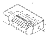
- FIG. 3 is a perspective view showing an overall image of the semiconductor laser module 1 manufactured by applying the bonding method according to the present embodiment.
- the semiconductor laser module 1 is a laser module attached to the end of the optical fiber 2 and includes a substrate 10, a submount 20, a CoS (Chip on Submount) 30, a fiber mount 40, and a case 50 as shown in FIG. 3. I have.
- a part of the top plate and the side plate of the case 50 is omitted.
- the substrate 10 is a bottom plate of the semiconductor laser module 1.
- a plate-like member having a rounded rectangular main surface is used as the substrate 10.
- the substrate 10 functions as a heat sink for dissipating heat generated inside the semiconductor laser module 1 (particularly CoS 30) to the outside of the semiconductor laser module 1.
- substrate 10 is comprised with material with high heat conductivity, for example, Cu (copper), for example.
- each convex portion 11a to 11d On the upper surface of the substrate 10, as shown in FIG. 3, four convex portions 11a to 11d are provided. These four convex portions 11 a to 11 d function as spacers for separating the lower surface of the submount 20 from the upper surface of the substrate 10. These four convex portions 11a to 11d are integrated with the substrate 10 formed by punching or cutting.
- the submount 20 is placed on the upper surface of the substrate 10.
- the submount 20 is a support that supports the CoS 30 and the fiber mount 40.
- a plate-shaped member having a rectangular main surface is used as the submount 20, and the lower surface of the submount 20 is parallel to the upper surface of the substrate 10.
- the long side of the main surface is arranged so as to be parallel to the long side of the main surface of the substrate 10.
- the submount 20 is joined to the upper surface of the substrate 10 by a soft solder 61 spreading between the lower surface of the submount 20 and the upper surface of the substrate 10.
- 90% Au—Sn solder is used as the soft solder 61 as will be described later.
- the CoS 30 and the fiber mount 40 are placed on the upper surface of the submount 20.
- the fiber mount 40 is disposed on the side from which the optical fiber 2 is drawn (right front side in FIG. 3, hereinafter referred to as “fiber side”), and the CoS 30 is the side from which the optical fiber 2 is drawn. It is arranged on the opposite side (the left rear side in FIG. 3, hereinafter referred to as “lead side”).
- CoS 30 is obtained by integrating a laser mount 31 and a semiconductor laser chip 32.
- the laser mount 31 is a support that supports the semiconductor laser chip 32.
- a plate-like member having a rectangular main surface is used as the laser mount 31, and the lower surface of the laser mount 31 is parallel to the upper surface of the submount 20, and The long side of the main surface is arranged so as to be parallel to the long side of the main surface of the submount 20.
- the laser mount 31 is joined to the upper surface of the submount 20 by hard solder 62 spreading between the lower surface of the laser mount 31 and the upper surface of the submount 20.
- 90% Au—Sn solder is used as the hard solder 62, as will be described later.
- a semiconductor laser chip 32 is mounted on the upper surface of the laser mount 31 as shown in FIG.
- the semiconductor laser chip 32 is a laser light source that emits laser light from its end face 32a.
- a high-power semiconductor laser mainly made of GaAs (gallium arsenide) and having a cavity length of 5 mm or more is used.
- the semiconductor laser chip 32 is disposed so that its extending direction is parallel to the long side of the main surface of the laser mount 31, and its lower surface is bonded to the upper surface of the laser mount 31.
- the semiconductor laser chip 32 is connected to a circuit formed on the upper surface of the laser mount 31 via a wire 33, and is driven by a current supplied from this circuit.
- the fiber mount 40 is a support that supports the optical fiber 2.
- a plate-shaped member having a rectangular main surface is used, and the lower surface of the fiber mount 40 is parallel to the submount 20 and The main surface is arranged so that the long side thereof is perpendicular to the long side of the main surface of the submount 20.
- the fiber mount 40 is joined to the upper surface of the submount 20 by hard solder 63 spreading between the lower surface of the fiber mount 40 and the upper surface of the submount 20.
- the optical fiber 2 drawn into the semiconductor laser module 1 through the insertion pipe 51 provided in the case 50 is placed on the fiber mount 40.
- the optical fiber 2 is disposed so that the tip 2 a processed into a wedge shape faces the end surface 32 a of the semiconductor laser chip 32, and is joined to the upper surface of the fiber mount 40 by the solder 64.
- Laser light emitted from the end face 32 a of the semiconductor laser chip 32 enters the optical fiber 2 from the tip 2 a and propagates through the optical fiber 2.
- an Au layer 31b and an Au layer 20b are formed on the lower surface of the laser mount 31 and the upper surface of the submount 20, respectively.
- the thicknesses of these Au layers 31b and 20b are determined as follows. That is, the mass of Sn contained in the Au—Sn solder 62 before joining, which is Au—Sn 90% solder, is x, the mass of Au contained in the Au—Sn solder 62 before joining is contained in y62, and the Au layer 31b.
- the mass of Au is y31b
- the mass of Au contained in the Au layer 20b is y20b
- the Au—Sn solder 62 after bonding functions as a hard solder, as already described with reference to FIG.
- Au—Sn solder 62 before bonding Au—Sn 90% solder formed in a plate shape is used as the Au—Sn 90% solder formed in a plate shape is used.
- the laser mount 31 and the submount 20 are joined by the following steps S1 to S8.
- Step S1 The submount 20 is placed on the heater stage.
- Step S2 Au—Sn solder 62 formed in a plate shape is placed on the substrate 10.
- Step S3 The laser mount 31 is placed on the Au—Sn solder 62.
- Process S4 Heating of the submount 20 by the heater stage is started.
- the temperature of the submount 20 gradually increases.
- the temperature of the submount 20 reaches 217 ° C.
- the Au—Sn solder 62 starts to melt from the submount 20 side.
- Au constituting the Au layer 31b and the Au layer 20b is diffused into the molten Au—Sn solder 62, and the weight percentage concentration of Sn in the molten Au—Sn solder 62 is 38.0% or more and 82.3% or less. become.
- the Au—Sn solder 62 is heated as high as possible within a range that does not adversely affect the semiconductor laser chip 32, that is, the Au—Sn solder 62 is heated to 240 ° C. to 250 ° C. It is desirable to heat to about ° C.
- Step S5 When the Au—Sn solder 62 is completely melted, the laser mount 31 is scrubbed. Note that scrubbing the laser mount 31 refers to sliding the laser mount 31 several times in a plane parallel to the upper surface of the submount 20. Thereby, bubbles mixed between the Au—Sn solder 62 and the laser mount 31 are eliminated.
- Process S6 Heating of the submount 20 by the heater stage is stopped. When the heating of the submount 20 by the heater stage is stopped, the temperature of the submount 20 gradually decreases.
- Process S7 The Au—Sn solder 62 is rapidly cooled. At this time, since the Sn weight percentage concentration in the molten Au—Sn solder 62 is 38.0% or more and 82.3% or less, the eutectic of ⁇ -AuSn and ⁇ -AuSn or ⁇ -AuSn and ⁇ -AuSn And a eutectic.
- the joining of the laser mount 31 and the submount 20 is realized.
- the Au—Sn solder 62 after joining becomes a hard solder having a large Young's modulus.
- the step of bonding the submount 20 to the substrate 10 is performed after the step of bonding the laser mount 31 to the submount 20.
- an Au layer 20a and an Au layer 10a are formed on the lower surface of the submount 20 and the upper surface of the substrate 10, respectively.
- the thicknesses of these Au layers 20a and 10a are determined as follows. That is, the mass of Sn contained in the Au—Sn solder 61 before joining is x, the mass of Au contained in the Au—Sn solder 61 before joining is y61, the mass of Au contained in the Au layer 20a is y20a, and the Au layer.
- the Au—Sn solder 61 after bonding functions as a soft solder, as already described with reference to FIG.
- Au—Sn solder 61 before joining Au—Sn 90% solder formed in a plate shape is used as the Au—Sn 90% solder formed in a plate shape is used.
- the submount 20 and the substrate 10 are joined by the following steps T1 to T8.
- Process T1 The substrate 10 is placed on the heater stage.
- Step T2 The Au—Sn solder 61 formed in a plate shape is placed on the substrate 10.
- Process T3 The submount 20 is placed on the Au—Sn solder 61.
- Process T4 Heating of the substrate 10 by the heater stage is started.
- the temperature of the substrate 10 gradually increases.
- the temperature of the substrate 10 reaches 217 ° C.
- the Au—Sn solder 61 starts to melt from the substrate 10 side.
- Au constituting the Au layer 20 diffuses into the melted Au—Sn solder 61, and the weight percentage concentration of Sn in the melted Au—Sn solder 61 becomes 82.3% or more and 90.0% or less.
- Process T6 Heating of the substrate 10 by the heater stage is stopped. When the heating of the substrate 10 by the heater stage is stopped, the temperature of the substrate 10 gradually decreases.
- the joining of the submount 20 and the substrate 10 is realized.
- the Au—Sn solder 61 after joining becomes a soft solder having a small Young's modulus.
- the joining method according to the present embodiment is a joining method in which the first member and the second member are joined with Au—Sn solder, and the weight of Sn in the Au—Sn solder after joining is the same.
- % Concentration is 38.0% or more and 82.3% or less.
- the Au—Sn solder after bonding is a hard solder containing a eutectic of ⁇ -AuSn and ⁇ -AuSn (the Sn wt% concentration in the Au—Sn solder after bonding is 55. 0% or more and 82.3% or less), or hard solder containing a eutectic of ⁇ -AuSn and ⁇ -AuSn (the Sn wt% concentration in the Au-Sn solder after bonding is 38.0) % Or more and 61.0% or less).
- Au—Sn 90% solder when used in combination with the Au layer formed on the bonding surface of the first member or the second member, it becomes possible to use Au—Sn 90% solder as hard solder after bonding.
- an Au layer is formed on at least one of the bonding surface of the first member before bonding and the bonding surface of the second member before bonding.
- an Au—Sn 90% solder can be easily used as a hard solder after joining simply by adjusting the thickness of the Au layer so that the mass of Au contained in the Au layer satisfies the above conditions. It becomes possible.
- the Au—Sn solder before bonding is preferably Au—Sn 90% solder.
- hard solder can be realized by using widely used Au-Sn 90% solder.
- the manufacturing method of the laser module including the joining process using the said joining method is also contained in the category of this embodiment.
- the present invention can be widely applied to the joining of members using Au—Sn solder (for example, Au—Sn 90% solder). In particular, it can be widely applied to the joining of optical components using Au—Sn 90% solder.
- Submount 30 CoS 31
- Laser mount 32 Semiconductor laser chip (laser light source) 40
Landscapes
- Engineering & Computer Science (AREA)
- Mechanical Engineering (AREA)
- Chemical & Material Sciences (AREA)
- Materials Engineering (AREA)
- Metallurgy (AREA)
- Organic Chemistry (AREA)
- Physics & Mathematics (AREA)
- Manufacturing & Machinery (AREA)
- Microelectronics & Electronic Packaging (AREA)
- Condensed Matter Physics & Semiconductors (AREA)
- General Physics & Mathematics (AREA)
- Electromagnetism (AREA)
- Optics & Photonics (AREA)
- Semiconductor Lasers (AREA)
- Die Bonding (AREA)
Abstract
本発明の接合方法は、2つの部材(A,B)をAu-Sn半田で接合する接合方法である。本発明の接合方法においては、接合後のAu-Sn半田(S')におけるSnの重量%濃度を、38.0%以上82.3%以下としている。
Description
本発明は、半田によって2つの部材を接合する接合方法に関する。また、そのような接合方法を用いた、レーザモジュールの製造方法に関する。
光ファイバにレーザ光を入射させる装置として、レーザモジュールが広く用いられている。レーザモジュールは、レーザ光を発するレーザ光源、レーザ光を受ける光ファイバ、及び、レーザ光源と光ファイバとの双方が取り付けられる放熱基板を備えている。レーザ光源及び光ファイバは、レーザ光源から発せられたレーザ光が光ファイバに効率よく入射するように位置合わせした上で放熱基板に固定される。
レーザモジュールでは、通常、レーザ光源と光ファイバとを直接的に放熱基板に接合するのではなく、先ず、レーザマウントとファイバマウントとを放熱基板に接合し、更に、レーザ光源と光ファイバとをレーザマウントとファイバマウントとに接合する構成が採用される。これらの部材の接合には、Au-Sn(金・錫)90%半田やAu-Sn20%半田などが頻用されている。このような構成を有する光ファイバを開示した文献としては、例えば、特許文献1が挙げられる。
また、特許文献2には、Snの重量%濃度が13%以下のAu-Sn半田を用いて、レーザモジュールを構成する複数の部材を、前に接合した半田を再溶融させることなく、順に接合する接合方法が開示されている。
しかしながら、上述したAu-Sn半田には以下のような問題があった。
すなわち、Au-Sn20%半田は、その融点が278℃と高いため、Au-Sn20%半田を用いて部材を接合すると、その部材に熱歪を生じさせる。したがって、半導体レーザチップなど、熱歪に弱い部材の接合には適さない。また、特許文献2に記載されたAu-Sn半田は、その融点が300℃以上であり、尚更、熱歪に弱い部材の接合には適さない。
一方、Au-Sn90%半田は、その融点が217℃であり、半導体レーザチップの接合にしばしば利用されるものである。しかしながら、Au-Sn90%半田は、ヤング率が小さい軟質半田(ソフトソルダ)であるため、部材の位置精度が低下し易いという問題があった。
本発明は、上記の課題に鑑みてなされたものであり、その目的は、Au-Sn90%半田などのAu-Sn半田を、接合後に硬質半田として使用し得る接合方法を実現することである。
上記課題を解決するために、本発明に係る接合方法は、第1の部材と第2の部材とをAu-Sn半田で接合する接合方法であって、接合後の上記Au-Sn半田におけるSnの重量%濃度が、38.0%以上82.3%以下である、ことを特徴とする。
上記の構成によれば、接合後のAu-Sn半田は、ε-AuSnとη-AuSnとの共晶を含む硬質半田(接合後の上記Au-Sn半田におけるSnの重量%濃度が、55.0%以上82.3%以下である場合)、又は、δ-AuSnとε-AuSnとの共晶を含む硬質半田(接合後の上記Au-Sn半田におけるSnの重量%濃度が、38.0%以上61.0%以下である場合)となる。また、第1の部材又は第2の部材の接合面に形成されたAu層と併用すれば、Au-Sn90%半田を接合後に硬質半田として使用することが可能になる。
本発明によれば、Au-Sn90%半田などのAu-Sn半田を、接合後に硬質半田として使用することができる。
〔接合方法の概要〕
本発明の一実施形態に係る接合方法について、図1を参照して説明する。本実施形態に係る接合方法は、2つの部材A,BをAu-Sn(金・錫)半田Sで接合する接合方法である。
本発明の一実施形態に係る接合方法について、図1を参照して説明する。本実施形態に係る接合方法は、2つの部材A,BをAu-Sn(金・錫)半田Sで接合する接合方法である。
なお、対象となる2つの部材A,Bは、それぞれ、少なくとも1つの平面を有していればよい。この場合、これらの平面(以下「接合面」と記載)同士をAu-Sn半田Sで接合する際に本実施形態に係る接合方法を適用することができる。部材A,Bの材料は特に限定されるものではないが、本実施形態においては、AlN(窒化アルミニウム)やCuW(銅タングステン)など、レーザモジュール等の光学装置に頻用される材料を想定する。
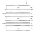
図1(a)は、2つの部材A,Bの接合前の状態を示す断面図である。
部材Aの接合面には、図1(a)に示すように、Au層MAが形成されている。同様に、部材Bの接合面にも、図1(a)に示すように、Au層MBが形成されている。これらのAu層MA,MBは、メッキや蒸着などによって部材A,Bの接合面に形成されたものであり、「メタライズ」と呼ばれることもある。
Au-Sn半田Sは、板状に成形されたAu-Sn90%半田である。Au-Sn半田Sの融点は217℃であり、熱的なストレスに弱い半導体レーザなどの接合にしばしば用いられるものである。
Au-Sn半田Sによる2つの部材A,Bの接合は、部材Aの接合面をAu-Sn半田Sの一方の主面に当接させ、かつ、部材Bの接合面をAu-Sn半田Sの他方の主面に当接させた状態で、部材Bをヒータステージ等で加熱することによって行われる。ヒータステージから部材Bに伝導した熱は、更に、部材BからAu-Sn半田Sに伝導し、Au-Sn半田Sの温度を上昇させる。
Au-Sn半田Sの温度が融点217℃を超えると、Au-Sn半田Sが溶融し、Au層MA~MBに含まれるAuが溶融したAu-Sn半田Sに拡散する。したがって、溶融状態にあるAu-Sn半田S”(不図示)におけるSnの重量%濃度は、接合前のAu-Sn半田SにおけるSnの重量%濃度よりも小さくなる。これは、Au層MA~MBから拡散したAuによって、溶融状態にあるAu-Sn半田S”に含まれるAuの量が増え、Au-Sn半田S”全体の中でSnが占める比率が減少するためである。
溶融状態にあるAu-Sn半田S”を冷却することによって、(1)η-AuSnとβ-Snとの共晶、(2)ε-AuSnとη-AuSnとの共晶、又は、(3)ε-AuSnとδ-AuSnとの共晶を析出させることができる。何れの共晶が析出するかは、溶融状態にあるAu-Sn半田S”におけるSnの重量%濃度によって決まる。Au-Sn半田S”を更に急冷すると、Au-Sn半田S”は、何れかの共晶組成を保ったまま凝固する。これにより、部材Aと部材Bとの接合が完了する。なお、溶融状態にあるAu-Sn半田S”から何れの共晶が析出するかについては、参照する図面を代えて後述する。
図1(b)は、2つの部材A,Bの接合後の状態を示す断面図である。
Au層MA~MBを構成するAuが全て溶融状態にあるAu-Sn半田S”に拡散した場合、図1(b)に示すように、接合後のAu-Sn半田S’を介して部材Aと部材Bとが接合されることになる。接合後のAu-Sn半田S’におけSnの重量%濃度は、溶融状態にあるAu-Sn半田S”の重量%濃度に等しく、また、接合前のAu-Sn半田SにおけるSnの重量%濃度よりも小さい。
Au層MA~MBを構成するAuが全て溶融状態にあるAu-Sn半田S”に拡散した場合、接合後のAu-Sn半田S’におけSnの重量%濃度は、以下のように与えられる。すなわち、接合前のAu-Sn半田Sに含まれるSnの質量をx、接合前のAu-Sn半田Sに含まれるAuの質量をyS、Au層MAに含まれるAuの質量をyMA、Au層MBに含まれるAuの質量をyMB、これらに含まれるAuの質量の合計をy=yS+yMA+yMBとすると、接合後のAu-Sn半田S’におけSnの重量%濃度P’は、P’=100×x/(x+y)で与えられる。
次に、接合後のSn-Au半田S’の物性について、図2を参照して説明する。図2は、Sn-Au合金の状態図(相図)である。図2の状態図において、横軸はSnの重量%濃度[wt%]、縦軸は温度[℃]を表す。
まず、接合後のSn-Au半田S’の融点について、図2を参照して説明する。
接合後のSn-Au半田S’の融点は、接合後のSn-Au半田S’におけるSnの重量%濃度に応じて決まる。具体的には、図2に示すように、Snの重量%濃度が38%以上であれば、Snの重量%濃度が小さくなるほど、接合後のSn-Au半田S’の融点は高くなる。上述したように、接合後のSn-Au半田S’におけるSnの重量%濃度は、接合前のSn-An半田SにおけるSnの重量%濃度よりも小さくなる。したがって、接合後のSn-Au半田S’の融点は、接合前のSn-An半田Sの融点よりも高くなる。
この性質は、部材の接合に極めて好都合な性質である。すなわち、部材Aに部材Bを接合し、さらに、部材Bに部材Cを接合する場合、既に接合した部材Aと部材Bとの間に介在するSn-Au半田S’の融点は、これから接合する部材Bと部材Cとの間に介在するSn-Au半田Sの融点217℃よりも高くなる。したがって、部材Bと部材Cとの間に介在するSn-Au半田Sを溶融させるために部材Bの温度を217℃まで上昇させても、既に接合した部材Aと部材Bとの間に介在するSn-Au半田S’が溶融することはない。
次に、接合後のSn-Au半田S’の共晶組成について、図2を参照して説明する。
図2から明らかなように、溶融状態にあるSn-Au半田S”におけるSnの重量%濃度が82.3%以上90.0%以下であるとき、接合後のSn-Au半田S’は、(1)η-AuSnとβ-Snとの共晶となる。一方、溶融状態にあるSn-Au半田S”におけるSnの重量%濃度が55.0%以上82.3%以下であるとき、接合後のSn-Au半田S’は、(2)ε-AuSnとη-AuSnとの共晶を含む。また、溶融状態にあるSn-Au半田S”におけるSnの重量%濃度が38.0%以上61.0%以下であるとき、接合後のSn-Au半田S’は、(3)δ-AuSnとε-AuSnとの共晶を含む。
ところで、ε-AuSnのヤング率は、103GPaであり、AuSn90%のヤング率(40GPa)やβ-Snのヤング率(41.4GPa)よりも高い。また、δ-AuSnのヤング率は、87±9GPaであり、やはり、AuSn90%のヤング率やβ-Snのヤング率よりも高い。したがって、溶融状態にあるSn-Au半田S”におけるSnの重量%濃度が38.0%以上82.3%以下となるようにすることによって、本来は軟質半田(ソフトソルダ)として機能するところのAu-Sn90%半田を、その2倍程度のヤング率を有する硬質半田(ハードソルダ)として機能させることができる。
この性質もまた、部材の接合に極めて好適な性質である。すなわち、対象となる部材の表面に形成するAu層の厚みを適宜変更することによって、接合箇所毎に接合強度を異ならせることができる。例えば、応力の緩和が重要な箇所では、Au層の厚みを薄くしてSn-Au半田を軟質半田として機能させ、部材の固定が重要な箇所では、Au層の厚みを厚くしてSn-Au半田を硬質半田として機能させることなどが可能である。
なお、接合前のAu-Sn半田Sに含まれるSnの質量をx、接合前のAu-Sn半田Sに含まれるAuの質量をyS、Au層MAに含まれるAuの質量をyMA、Au層MBに含まれるAuの質量をyMB、これらに含まれるAuの質量の合計をy=yS+yMA+yMBとすると、Au-Sn半田Sを硬質半田として機能させるための条件は、0.380≦x/(x+y)≦0.823と表現することができる。
〔適用例〕
次に、本実施形態に係る接合方法の適用例について、図3~図4を参照して説明する。
次に、本実施形態に係る接合方法の適用例について、図3~図4を参照して説明する。
まず、本実施形態に係る接合方法を適用して製造する半導体レーザモジュール1の構成について、図3を参照して説明する。図3は、本実施形態に係る接合方法を適用して製造する半導体レーザモジュール1の全体像を示す斜視図である。
半導体レーザモジュール1は、光ファイバ2の末端に装着されるレーザモジュールであり、図3に示すように、基板10、サブマウント20、CoS(Chip on Submount)30、ファイバマウント40、及びケース50を備えている。なお、図3においては、半導体レーザモジュール1の内部の構造を明らかにするために、ケース50の天板及び側板の一部を省略している。
基板10は、半導体レーザモジュール1の底板である。本適用例においては、図3に示すように、基板10として、主面が角丸矩形の板状部材を用いる。基板10は、半導体レーザモジュール1の内部(特にCoS30)で発生した熱を半導体レーザモジュール1の外部に放熱するためのヒートシンクとして機能する。このため、基板10は、熱伝導率の高い材料、例えば、例えばCu(銅)により構成される。
基板10の上面には、図3に示すように、4つの凸部11a~11dが設けられている。これらの4つの凸部11a~11dは、サブマウント20の下面を基板10の上面から離間させるためのスペーサとして機能する。これらの4つの凸部11a~11dは、打ち抜き加工や削り出し加工などによって成形された、基板10と一体のものである。
基板10の上面には、図3に示すように、サブマウント20が載置される。
サブマウント20は、CoS30及びファイバマウント40を支持する支持体である。本適用例においては、図3に示すように、サブマウント20として、主面が矩形の板状部材を用い、このサブマウント20を、その下面が基板10の上面と平行になり、かつ、その主面の長辺が基板10の主面の長辺と平行になるように配置する。サブマウント20は、その下面と基板10の上面との間に広がった軟質半田61によって、基板10の上面に接合される。サブマウント20と基板10との接合に際しては、後述するように、Au-Sn半田90%を軟質半田61として利用する。
サブマウント20の上面には、図3に示すように、CoS30とファイバマウント40とが載置される。サブマウント20の上面において、ファイバマウント40は、光ファイバ2が引き出される側(図3において右手前側、以下では「ファイバ側」と記載)に配置され、CoS30は、光ファイバ2が引き出される側と反対側(図3において左奥側、以下では「リード側」と記載)に配置される。
CoS30は、レーザマウント31と半導体レーザチップ32とが一体化されたものである。
レーザマウント31は、半導体レーザチップ32を支持する支持体である。本適用例においては、図3に示すように、レーザマウント31として、主面が矩形状の板状部材を用い、このレーザマウント31を、その下面がサブマウント20の上面と平行になり、かつ、その主面の長辺がサブマウント20の主面の長辺と平行になるように配置する。レーザマウント31は、その下面とサブマウント20の上面との間に広がった硬質半田62によって、サブマウント20の上面に接合される。レーザマウント31とサブマウント20との接合に際しては、後述するように、Au-Sn半田90%を硬質半田62として利用する。
レーザマウント31の上面には、図3に示すように、半導体レーザチップ32が載置される。半導体レーザチップ32は、その端面32aからレーザ光を発するレーザ光源である。本適用例においては、主にGaAs(ガリウム砒素)からなる、5mm以上のキャビティ長を有する高出力半導体レーザを用いる。半導体レーザチップ32は、図3に示すように、その延在方向がレーザマウント31の主面の長辺と平行になるように配置され、その下面がレーザマウント31の上面に接合されている。また、半導体レーザチップ32は、図3に示すように、ワイヤ33を介してレーザマウント31の上面に形成された回路に接続されており、この回路から供給された電流によって駆動される。
ファイバマウント40は、光ファイバ2を支持する支持体である。本適用例においては、ファイバマウント40として、図3に示すように、主面が矩形状の板状部材を用い、このファイバマウント40を、その下面がサブマウント20と平行になり、かつ、その主面の長辺がサブマウント20の主面の長辺と垂直になるように配置する。ファイバマウント40は、その下面とサブマウント20の上面との間に広がった硬質半田63によって、サブマウント20の上面に接合される。
ファイバマウント40には、図3に示すように、ケース50に設けられた挿通パイプ51を通して半導体レーザモジュール1の内部に引き込まれた光ファイバ2が載置される。光ファイバ2は、楔状に加工された先端2aが半導体レーザチップ32の端面32aに正対するように配置され、半田64によってファイバマウント40の上面に接合される。半導体レーザチップ32の端面32aから発せられたレーザ光は、先端2aから光ファイバ2に入射し、光ファイバ2内を伝搬する。
次に、本実施形態に係る接合方法の適用したレーザモジュール1の製造方法について、図4を参照して説明する。ここでは、特に、サブマウント20を基板10に接合する工程と、レーザマウント31をサブマウント20に接合する工程とに注目する。
まず、レーザマウント31の下面をサブマウント20の上面に接合する工程について説明する。
レーザマウント31をサブマウント20に接合する前に、図4に示すように、レーザマウント31の下面及びサブマウント20の上面に、それぞれ、Au層31b及びAu層20bを形成する。これらのAu層31b,20bの厚みは、以下のように決める。すなわち、Au-Sn90%半田である接合前のAu-Sn半田62に含まれるSnの質量をx、同じく接合前のAu-Sn半田62に含まれるAuの質量をy62、Au層31bに含まれるAuの質量をy31b、Au層20bに含まれるAuの質量をy20b、これらに含まれるAuの質量の合計をy=y62+y31b+y20bとして、0.380≦x/(x+y)≦0.823となるように決める。この場合、接合後のAu-Sn半田62が硬質半田として機能することは、図2を参照して既に説明したとおりである。なお、接合前のAu-Sn半田62としては、板状に形成されたAu-Sn90%半田を利用する。
上記の準備を行ったうえで、以下の工程S1~S8によって、レーザマウント31とサブマウント20とを接合する。
工程S1:サブマウント20をヒータステージ上に載置する。
工程S2:板状に成形されたAu-Sn半田62を基板10上に載置する。
工程S3:レーザマウント31をAu-Sn半田62上に載置する。
工程S4:ヒータステージによるサブマウント20の加熱を開始する。
ヒータステージによるサブマウント20の加熱を開始すると、サブマウント20の温度が次第に上昇する。サブマウント20の温度が217℃に達すると、Au-Sn半田62がサブマウント20側から溶融し始める。この際、Au層31b及びAu層20bを構成するAuが溶融したAu-Sn半田62に拡散し、溶融したAu-Sn半田62におけるSnの重量%濃度が38.0%以上82.3%以下になる。なお、Auの拡散を促進するために、半導体レーザチップ32への悪影響が生じない範囲でAu-Sn半田62をできるだけ高温になるよう加熱すること、すなわち、Au-Sn半田62を240℃~250℃程度まで加熱することが望ましい。
工程S5:Au-Sn半田62が完全に溶融したら、レーザマウント31をスクラブする。なお、レーザマウント31をスクラブするとは、レーザマウント31をサブマウント20の上面と平行な面内で何度か摺動させることを指す。これにより、Au-Sn半田62とレーザマウント31との間に混入した気泡を排除する。
工程S6:ヒータステージによるサブマウント20の加熱を停止する。ヒータステージによるサブマウント20の加熱を停止すると、サブマウント20の温度が次第に下降する。
工程S7:Au-Sn半田62を急冷する。この際、溶融したAu-Sn半田62におけるSnの重量%濃度が38.0%以上82.3%以下なので、ε-AuSnとη-AuSnとの共晶、又は、δ-AuSnとε-AuSnとの共晶が形成される。
以上のようにして、レーザマウント31とサブマウント20との接合が実現される。接合後のAu-Sn半田62は、ヤング率の大きい硬質半田となる。
次に、サブマウント20の下面を基板10の上面に接合する工程について説明する。なお、サブマウント20を基板10に接合する工程は、レーザマウント31をサブマウント20に接合する工程の後に行われる。
サブマウント20を基板10に接合する前に、サブマウント20の下面及び基板10の上面に、それぞれ、Au層20a及びAu層10aを形成する。これらのAu層20a,10aの厚みは、以下のように決める。すなわち、接合前のAu-Sn半田61に含まれるSnの質量をx、接合前のAu-Sn半田61に含まれるAuの質量をy61、Au層20aに含まれるAuの質量をy20a、Au層10aに含まれるAuの質量をy10a、これらに含まれるAuの質量の合計をy=y61+y20a+y10aとして、0.823≦x/(x+y)≦0.900を満たすように決める。この場合、接合後のAu-Sn半田61が軟質半田として機能することは、図2を参照して既に説明したとおりである。なお、接合前のAu-Sn半田61としては、板状に形成されたAu-Sn90%半田を利用する。
上記の準備を行ったうえで、以下の工程T1~T8によって、サブマウント20と基板10とを接合する。
工程T1:基板10をヒータステージ上に載置する。
工程T2:板状に成形されたAu-Sn半田61を基板10上に載置する。
工程T3:サブマウント20をAu-Sn半田61上に載置する。
工程T4:ヒータステージによる基板10の加熱を開始する。
ヒータステージによる基板10の加熱を開始すると、基板10の温度が次第に上昇する。基板10の温度が217℃に達すると、Au-Sn半田61が基板10側から溶融し始める。この際、Au層20を構成するAuが溶融したAu-Sn半田61に拡散し、溶融したAu-Sn半田61におけるSnの重量%濃度が82.3%以上90.0%以下になる。
工程T5:Au-Sn半田61が完全に溶融したら、サブマウント20をスクラブする。
工程T6:ヒータステージによる基板10の加熱を停止する。ヒータステージによる基板10の加熱を停止すると、基板10の温度が次第に下降する。
工程T7:Au-Sn半田61を急冷する。この際、溶融したAu-Sn半田61におけるSnの重量%濃度が82.3%以上90.0%以下なので、η-AuSnとβ-Snとの共晶が形成される。
以上のようにして、サブマウント20と基板10との接合が実現される。接合後のAu-Sn半田61は、ヤング率の小さい軟質半田となる。
〔まとめ〕
以上のように、本実施形態に係る接合方法は、第1の部材と第2の部材とをAu-Sn半田で接合する接合方法であって、接合後の上記Au-Sn半田におけるSnの重量%濃度が、38.0%以上82.3%以下である、ことを特徴とする。
以上のように、本実施形態に係る接合方法は、第1の部材と第2の部材とをAu-Sn半田で接合する接合方法であって、接合後の上記Au-Sn半田におけるSnの重量%濃度が、38.0%以上82.3%以下である、ことを特徴とする。
上記の構成によれば、接合後のAu-Sn半田は、ε-AuSnとη-AuSnとの共晶を含む硬質半田(接合後の上記Au-Sn半田におけるSnの重量%濃度が、55.0%以上82.3%以下である場合)、又は、δ-AuSnとε-AuSnとの共晶を含む硬質半田(接合後の上記Au-Sn半田におけるSnの重量%濃度が、38.0%以上61.0%以下である場合)となる。また、第1の部材又は第2の部材の接合面に形成されたAu層と併用すれば、Au-Sn90%半田を接合後に硬質半田として使用することが可能になる。
本実施形態に係る接合方法においては、接合前の上記第1の部材の接合面、及び、接合前の上記第2の部材の接合面の少なくとも何れか一方には、Au層が形成されており、接合前の上記Au-Sn半田に含まれるSnの質量をx、接合前の上記Au-Sn半田及び上記Au層に含まれるAuの合計質量をyとしたときに、0.380≦x/(x+y)≦0.823となる、ことが好ましい。
上記の構成によれば、上記Au層に含まれるAuの質量が上記条件を満たすよう、上記Au層の厚などを調整するだけで、容易にAu-Sn90%半田を接合後に硬質半田として使用することが可能になる。
本実施形態に係る接合方法において、接合前の上記Au-Sn半田は、Au-Sn90%半田である、ことが好ましい。
上記構成によれば、広く利用されているAu-Sn90%半田を使って、硬質半田を実現することができる。
なお、上記接合方法を用いた接合工程を含むレーザモジュールの製造方法も本実施形態の範疇に含まれる。
〔付記事項〕
本発明は上述した実施形態に限定されるものではなく、請求項に示した範囲で種々の変更が可能である。すなわち、請求項に示した範囲で適宜変更した技術的手段を組み合わせて得られる実施形態についても本発明の技術的範囲に含まれる。
本発明は上述した実施形態に限定されるものではなく、請求項に示した範囲で種々の変更が可能である。すなわち、請求項に示した範囲で適宜変更した技術的手段を組み合わせて得られる実施形態についても本発明の技術的範囲に含まれる。
本発明は、Au-Sn半田(例えば、Au-Sn90%半田)による部材の接合に広く適用することができる。特に、Au-Sn90%半田による光学部品の接合に広く適用することができる。
A 部材(第1の部材)
MA Au層
B 部材(第2の部材)
MB Au層
S Au-Sn半田(接合前)(Au-Sn90%半田)
S’ Au-Sn半田(接合後)
1 半導体レーザモジュール(レーザモジュール)
10 基板
11a~11d 凸部
20 サブマウント
30 CoS
31 レーザマウント
32 半導体レーザチップ(レーザ光源)
40 ファイバマウント
50 ケース
61 軟質半田
62 硬質半田
MA Au層
B 部材(第2の部材)
MB Au層
S Au-Sn半田(接合前)(Au-Sn90%半田)
S’ Au-Sn半田(接合後)
1 半導体レーザモジュール(レーザモジュール)
10 基板
11a~11d 凸部
20 サブマウント
30 CoS
31 レーザマウント
32 半導体レーザチップ(レーザ光源)
40 ファイバマウント
50 ケース
61 軟質半田
62 硬質半田
Claims (6)
- 第1の部材と第2の部材とをAu-Sn半田で接合する接合方法であって、
接合後の上記Au-Sn半田におけるSnの重量%濃度が、38.0%以上82.3%以下である、ことを特徴とする接合方法。 - 接合前の上記第1の部材の接合面、及び、接合前の上記第2の部材の接合面の少なくとも何れか一方に、Au層を形成する形成工程と、
接合前の上記第1の部材の接合面、及び、接合前の上記第2の部材の接合面の両方に当接した上記Au-Sn半田を溶融させる溶融工程とを含み、
接合前の上記Au-Sn半田に含まれるSnの質量をx、接合前の上記Au-Sn半田及び上記Au層に含まれるAuの合計質量をyとしたときに、0.380≦x/(x+y)≦0.823となる、
ことを特徴とする請求項1に記載の接合方法。 - 接合前の上記Au-Sn半田は、Au-Sn90%半田である、
ことを特徴とする請求項1又は2に記載の接合方法。 - 接合後の上記Au-Sn半田におけるSnの重量%濃度が、55.0%以上82.3%以下である、
ことを特徴とする請求項1から3までの何れか1項に記載の接合方法。 - 接合後の上記Au-Sn半田におけるSnの重量%濃度が、38.0%以上61.0%以下である、
ことを特徴とする請求項1から3までの何れか1項に記載の接合方法。 - レーザ光源が載置されたレーザマウントと、上記レーザマウントが載置されたサブマウントと、上記サブマウントが載置された基板とを備えたレーザモジュールの製造方法であって、
請求項1から5までの何れか1項に記載の接合方法を用いて、上記レーザマウントと上記サブマウントとをAu-Sn半田で接合する接合工程を含んでいる、
ことを特徴とするレーザモジュールの製造方法。
Priority Applications (2)
| Application Number | Priority Date | Filing Date | Title |
|---|---|---|---|
| CN201280029262.XA CN103608908B (zh) | 2011-06-16 | 2012-04-04 | 接合方法和制造方法 |
| US14/103,050 US20140097232A1 (en) | 2011-06-16 | 2013-12-11 | Bonding method and production method |
Applications Claiming Priority (2)
| Application Number | Priority Date | Filing Date | Title |
|---|---|---|---|
| JP2011134549A JP5281122B2 (ja) | 2011-06-16 | 2011-06-16 | 接合方法、及び、製造方法 |
| JP2011-134549 | 2011-06-16 |
Related Child Applications (1)
| Application Number | Title | Priority Date | Filing Date |
|---|---|---|---|
| US14/103,050 Continuation US20140097232A1 (en) | 2011-06-16 | 2013-12-11 | Bonding method and production method |
Publications (1)
| Publication Number | Publication Date |
|---|---|
| WO2012172854A1 true WO2012172854A1 (ja) | 2012-12-20 |
Family
ID=47356852
Family Applications (1)
| Application Number | Title | Priority Date | Filing Date |
|---|---|---|---|
| PCT/JP2012/059153 Ceased WO2012172854A1 (ja) | 2011-06-16 | 2012-04-04 | 接合方法、及び、製造方法 |
Country Status (4)
| Country | Link |
|---|---|
| US (1) | US20140097232A1 (ja) |
| JP (1) | JP5281122B2 (ja) |
| CN (1) | CN103608908B (ja) |
| WO (1) | WO2012172854A1 (ja) |
Cited By (1)
| Publication number | Priority date | Publication date | Assignee | Title |
|---|---|---|---|---|
| EP3127197A4 (en) * | 2014-03-31 | 2017-12-27 | IPG Photonics Corporation | High-power laser diode packaging method and laser diode module |
Families Citing this family (1)
| Publication number | Priority date | Publication date | Assignee | Title |
|---|---|---|---|---|
| JP2017011043A (ja) * | 2015-06-18 | 2017-01-12 | 株式会社フジクラ | レーザ装置、及び、レーザ装置の製造方法 |
Citations (4)
| Publication number | Priority date | Publication date | Assignee | Title |
|---|---|---|---|---|
| JP2003200289A (ja) * | 2001-09-27 | 2003-07-15 | Furukawa Electric Co Ltd:The | 部材の接合方法、その方法で得られた接合部材 |
| JP2006278463A (ja) * | 2005-03-28 | 2006-10-12 | Dowa Mining Co Ltd | サブマウント |
| JP2008080393A (ja) * | 2006-09-29 | 2008-04-10 | Toshiba Corp | 包晶系合金を用いた接合体、接合方法、及び半導体装置 |
| JP2011167761A (ja) * | 2010-01-25 | 2011-09-01 | Mitsubishi Materials Corp | Au−Sn合金はんだペースト、およびこれにより形成されるAu−Sn合金はんだ |
Family Cites Families (23)
| Publication number | Priority date | Publication date | Assignee | Title |
|---|---|---|---|---|
| US5568892A (en) * | 1994-06-16 | 1996-10-29 | Lucent Technologies Inc. | Alignment and bonding techniques |
| DE69838586T2 (de) * | 1997-06-04 | 2008-07-24 | Ibiden Co., Ltd., Ogaki | Lötelement für gedruckte leiterplatten |
| JP3139423B2 (ja) * | 1997-09-02 | 2001-02-26 | 日本電気株式会社 | 光素子の実装構造 |
| US6204454B1 (en) * | 1997-12-27 | 2001-03-20 | Tdk Corporation | Wiring board and process for the production thereof |
| JP2915888B1 (ja) * | 1998-01-28 | 1999-07-05 | 日本特殊陶業株式会社 | 配線基板及びその製造方法 |
| JP2000228006A (ja) * | 1999-02-05 | 2000-08-15 | Alps Electric Co Ltd | ボンディングパットおよびバンプを用いた接合体、および磁気ヘッド装置 |
| JP2001024085A (ja) * | 1999-07-12 | 2001-01-26 | Nec Corp | 半導体装置 |
| US6758610B2 (en) * | 2001-12-10 | 2004-07-06 | Jds Uniphase Corporation | Optical component attachment to optoelectronic packages |
| JP3757881B2 (ja) * | 2002-03-08 | 2006-03-22 | 株式会社日立製作所 | はんだ |
| US6660548B2 (en) * | 2002-03-27 | 2003-12-09 | Intel Corporation | Packaging of multiple active optical devices |
| US6630251B1 (en) * | 2002-09-23 | 2003-10-07 | Delphi Technologies, Inc. | Leach-resistant solder alloys for silver-based thick-film conductors |
| JP2004289011A (ja) * | 2003-03-24 | 2004-10-14 | Sumitomo Electric Ind Ltd | 発光モジュール |
| WO2006049024A1 (ja) * | 2004-11-01 | 2006-05-11 | Senju Metal Industry Co., Ltd | 高温鉛フリーはんだおよび半導体素子収納用パッケージ |
| JP4617902B2 (ja) * | 2005-01-31 | 2011-01-26 | 信越半導体株式会社 | 発光素子及び発光素子の製造方法 |
| US7628871B2 (en) * | 2005-08-12 | 2009-12-08 | Intel Corporation | Bulk metallic glass solder material |
| US7939939B1 (en) * | 2007-06-11 | 2011-05-10 | Texas Instruments Incorporated | Stable gold bump solder connections |
| JP5079474B2 (ja) * | 2007-11-29 | 2012-11-21 | シャープ株式会社 | キャップ部材およびそれを用いた半導体装置 |
| US8475056B2 (en) * | 2009-07-28 | 2013-07-02 | Jds Uniphase Corporation | Semiconductor device assembly |
| US8841766B2 (en) * | 2009-07-30 | 2014-09-23 | Taiwan Semiconductor Manufacturing Company, Ltd. | Cu pillar bump with non-metal sidewall protection structure |
| CN102844943A (zh) * | 2010-03-31 | 2012-12-26 | 株式会社藤仓 | 激光装置 |
| US8232193B2 (en) * | 2010-07-08 | 2012-07-31 | Taiwan Semiconductor Manufacturing Company, Ltd. | Method of forming Cu pillar capped by barrier layer |
| JP5102380B2 (ja) * | 2011-02-24 | 2012-12-19 | 株式会社フジクラ | ファイバマウント装置、及び、それを用いた光モジュール、及び、光モジュールの製造方法 |
| JP2013004752A (ja) * | 2011-06-16 | 2013-01-07 | Fujikura Ltd | レーザモジュール |
-
2011
- 2011-06-16 JP JP2011134549A patent/JP5281122B2/ja active Active
-
2012
- 2012-04-04 WO PCT/JP2012/059153 patent/WO2012172854A1/ja not_active Ceased
- 2012-04-04 CN CN201280029262.XA patent/CN103608908B/zh not_active Expired - Fee Related
-
2013
- 2013-12-11 US US14/103,050 patent/US20140097232A1/en not_active Abandoned
Patent Citations (4)
| Publication number | Priority date | Publication date | Assignee | Title |
|---|---|---|---|---|
| JP2003200289A (ja) * | 2001-09-27 | 2003-07-15 | Furukawa Electric Co Ltd:The | 部材の接合方法、その方法で得られた接合部材 |
| JP2006278463A (ja) * | 2005-03-28 | 2006-10-12 | Dowa Mining Co Ltd | サブマウント |
| JP2008080393A (ja) * | 2006-09-29 | 2008-04-10 | Toshiba Corp | 包晶系合金を用いた接合体、接合方法、及び半導体装置 |
| JP2011167761A (ja) * | 2010-01-25 | 2011-09-01 | Mitsubishi Materials Corp | Au−Sn合金はんだペースト、およびこれにより形成されるAu−Sn合金はんだ |
Cited By (1)
| Publication number | Priority date | Publication date | Assignee | Title |
|---|---|---|---|---|
| EP3127197A4 (en) * | 2014-03-31 | 2017-12-27 | IPG Photonics Corporation | High-power laser diode packaging method and laser diode module |
Also Published As
| Publication number | Publication date |
|---|---|
| CN103608908A (zh) | 2014-02-26 |
| JP2013004751A (ja) | 2013-01-07 |
| CN103608908B (zh) | 2017-05-10 |
| JP5281122B2 (ja) | 2013-09-04 |
| US20140097232A1 (en) | 2014-04-10 |
Similar Documents
| Publication | Publication Date | Title |
|---|---|---|
| JP5253495B2 (ja) | 光モジュール | |
| US8193634B2 (en) | Mounted semiconductor device and a method for making the same | |
| KR101142561B1 (ko) | 레이저 광원 모듈 | |
| WO2012172855A1 (ja) | レーザモジュール | |
| JP5622721B2 (ja) | 少なくとも一つの半導体素子、特に、レーザ素子または発光ダイオード素子を有する熱伝達デバイス、およびその組立方法 | |
| JP2013004752A5 (ja) | レーザモジュール、及び、その製造方法 | |
| JP2016054279A (ja) | 半導体レーザ | |
| CN106134018A (zh) | 高功率激光二极管封装方法和激光二极管模块 | |
| CN102844943A (zh) | 激光装置 | |
| JP6652856B2 (ja) | 半導体レーザモジュール及びその製造方法 | |
| JP5509317B2 (ja) | レーザ装置およびその製造方法 | |
| JP5281122B2 (ja) | 接合方法、及び、製造方法 | |
| JP5589112B2 (ja) | 接合方法 | |
| JP6906721B1 (ja) | 半導体レーザ装置 | |
| JP2015185667A (ja) | 半導体レーザモジュール、及び、半導体レーザモジュールの製造方法 | |
| JP2007305977A (ja) | 半導体レーザ装置及びその製造方法 | |
| JP5111644B2 (ja) | 光ファイバ固定方法、及びレーザモジュールの製造方法 | |
| TWI411183B (zh) | 雷射二極體元件 | |
| CN106711754A (zh) | 一种高功率半导体激光器的封装结构及其制备方法 | |
| Pliska et al. | Bonding semiconductor laser chips: substrate material figure of merit and die attach layer influence | |
| JP4350382B2 (ja) | 半導体レーザ装置及びその製造方法 | |
| JP2007157960A (ja) | 半導体レーザ装置の製造方法 |
Legal Events
| Date | Code | Title | Description |
|---|---|---|---|
| 121 | Ep: the epo has been informed by wipo that ep was designated in this application |
Ref document number: 12800864 Country of ref document: EP Kind code of ref document: A1 |
|
| NENP | Non-entry into the national phase |
Ref country code: DE |
|
| 122 | Ep: pct application non-entry in european phase |
Ref document number: 12800864 Country of ref document: EP Kind code of ref document: A1 |