WO2012169160A1 - 液晶表示装置、および液晶表示装置の駆動回路 - Google Patents
液晶表示装置、および液晶表示装置の駆動回路 Download PDFInfo
- Publication number
- WO2012169160A1 WO2012169160A1 PCT/JP2012/003595 JP2012003595W WO2012169160A1 WO 2012169160 A1 WO2012169160 A1 WO 2012169160A1 JP 2012003595 W JP2012003595 W JP 2012003595W WO 2012169160 A1 WO2012169160 A1 WO 2012169160A1
- Authority
- WO
- WIPO (PCT)
- Prior art keywords
- end side
- liquid crystal
- display device
- voltage
- crystal display
- Prior art date
- Legal status (The legal status is an assumption and is not a legal conclusion. Google has not performed a legal analysis and makes no representation as to the accuracy of the status listed.)
- Ceased
Links
Images



Classifications
-
- G—PHYSICS
- G09—EDUCATION; CRYPTOGRAPHY; DISPLAY; ADVERTISING; SEALS
- G09G—ARRANGEMENTS OR CIRCUITS FOR CONTROL OF INDICATING DEVICES USING STATIC MEANS TO PRESENT VARIABLE INFORMATION
- G09G3/00—Control arrangements or circuits, of interest only in connection with visual indicators other than cathode-ray tubes
- G09G3/20—Control arrangements or circuits, of interest only in connection with visual indicators other than cathode-ray tubes for presentation of an assembly of a number of characters, e.g. a page, by composing the assembly by combination of individual elements arranged in a matrix no fixed position being assigned to or needed to be assigned to the individual characters or partial characters
- G09G3/34—Control arrangements or circuits, of interest only in connection with visual indicators other than cathode-ray tubes for presentation of an assembly of a number of characters, e.g. a page, by composing the assembly by combination of individual elements arranged in a matrix no fixed position being assigned to or needed to be assigned to the individual characters or partial characters by control of light from an independent source
- G09G3/36—Control arrangements or circuits, of interest only in connection with visual indicators other than cathode-ray tubes for presentation of an assembly of a number of characters, e.g. a page, by composing the assembly by combination of individual elements arranged in a matrix no fixed position being assigned to or needed to be assigned to the individual characters or partial characters by control of light from an independent source using liquid crystals
- G09G3/3611—Control of matrices with row and column drivers
- G09G3/3648—Control of matrices with row and column drivers using an active matrix
-
- G—PHYSICS
- G09—EDUCATION; CRYPTOGRAPHY; DISPLAY; ADVERTISING; SEALS
- G09G—ARRANGEMENTS OR CIRCUITS FOR CONTROL OF INDICATING DEVICES USING STATIC MEANS TO PRESENT VARIABLE INFORMATION
- G09G2300/00—Aspects of the constitution of display devices
- G09G2300/08—Active matrix structure, i.e. with use of active elements, inclusive of non-linear two terminal elements, in the pixels together with light emitting or modulating elements
- G09G2300/0876—Supplementary capacities in pixels having special driving circuits and electrodes instead of being connected to common electrode or ground; Use of additional capacitively coupled compensation electrodes
-
- G—PHYSICS
- G09—EDUCATION; CRYPTOGRAPHY; DISPLAY; ADVERTISING; SEALS
- G09G—ARRANGEMENTS OR CIRCUITS FOR CONTROL OF INDICATING DEVICES USING STATIC MEANS TO PRESENT VARIABLE INFORMATION
- G09G2320/00—Control of display operating conditions
- G09G2320/02—Improving the quality of display appearance
- G09G2320/0242—Compensation of deficiencies in the appearance of colours
-
- G—PHYSICS
- G09—EDUCATION; CRYPTOGRAPHY; DISPLAY; ADVERTISING; SEALS
- G09G—ARRANGEMENTS OR CIRCUITS FOR CONTROL OF INDICATING DEVICES USING STATIC MEANS TO PRESENT VARIABLE INFORMATION
- G09G3/00—Control arrangements or circuits, of interest only in connection with visual indicators other than cathode-ray tubes
- G09G3/20—Control arrangements or circuits, of interest only in connection with visual indicators other than cathode-ray tubes for presentation of an assembly of a number of characters, e.g. a page, by composing the assembly by combination of individual elements arranged in a matrix no fixed position being assigned to or needed to be assigned to the individual characters or partial characters
- G09G3/34—Control arrangements or circuits, of interest only in connection with visual indicators other than cathode-ray tubes for presentation of an assembly of a number of characters, e.g. a page, by composing the assembly by combination of individual elements arranged in a matrix no fixed position being assigned to or needed to be assigned to the individual characters or partial characters by control of light from an independent source
- G09G3/36—Control arrangements or circuits, of interest only in connection with visual indicators other than cathode-ray tubes for presentation of an assembly of a number of characters, e.g. a page, by composing the assembly by combination of individual elements arranged in a matrix no fixed position being assigned to or needed to be assigned to the individual characters or partial characters by control of light from an independent source using liquid crystals
- G09G3/3611—Control of matrices with row and column drivers
- G09G3/3696—Generation of voltages supplied to electrode drivers
Definitions
- the present invention relates to a liquid crystal display device that displays a color image.
- an image signal voltage corresponding to the display image is applied to the pixel electrode, and light that has passed through, for example, three color filters of red (R), green (G), and blue (B). Is displayed by synthesizing.
- R red
- G green
- B blue
- the transmittance of the color filter is different for each color, the luminance of each color does not become the same even when the same image signal voltage is applied to the pixel electrode of each color. Therefore, for example, a technique for adjusting the characteristics of the voltage applied to the pixel electrode and the transmittance of each color by changing the size of the auxiliary capacitor connected in parallel with the liquid crystal capacitor for each color is known (for example, Patent Documents 1 and 2).
- the characteristics of the voltage applied to the pixel electrode and the transmittance can be adjusted. However, the adjustment is performed uniformly for all the liquid crystal panels. For example, when the characteristics of the applied voltage and the transmittance vary for each liquid crystal panel, the adjustment cannot be made for each liquid crystal panel.
- the present invention has been made in view of such a point, and an object thereof is to make it possible to easily adjust the characteristics of the applied voltage and transmittance to the pixel electrode for each color.
- the first invention is Pixel electrodes provided for each of a plurality of types of colors; A counter electrode provided facing the pixel electrode; An auxiliary capacitor having one end connected to each pixel electrode, A liquid crystal display device in which luminance is displayed according to a voltage between the pixel electrode and the counter electrode, The other end side voltage wiring which can apply the other end side voltage different for each color is connected to the other end of the auxiliary capacitor.
- the voltage of the pixel electrode changes.
- the other end side voltage to be applied can be different for each color. Therefore, for example, even when the same image signal voltage is applied to pixel electrodes of a plurality of types of colors, the voltage of the pixel electrodes can be changed to be different for each color. Therefore, it is possible to easily adjust the characteristics of the voltage applied to the pixel electrode and the transmittance for each color.
- the second invention is A liquid crystal display device according to a first invention,
- the other end side voltage wiring is provided for only a part of a plurality of kinds of colors.
- the characteristics of the applied voltage and the transmittance to the pixel electrode for each color are easy in the relative relationship between the color where the other end side voltage wiring is not provided and the provided color. Can be adjusted.
- the aperture ratio can be easily kept large.
- the third invention is A liquid crystal display device according to a first invention,
- the other end side voltage wiring is provided in common for some of the plurality of colors.
- the fourth invention is: A liquid crystal display device according to any one of the first to third inventions, Furthermore, a drive circuit is provided that switches the other end side voltage different from each other during the application of the image signal voltage to the pixel electrode and after the application is finished, and applies the other end side voltage wiring to the other end side voltage wiring, At least one of the different other-end side voltages is different for each color.
- the fifth invention is: A liquid crystal display device according to a fourth invention, The other end side voltage is configured to be settable.
- the sixth invention is: A liquid crystal display device according to a fifth invention, The other end side voltage is configured to be variably set according to a control signal.
- the seventh invention A liquid crystal display device according to any one of the fourth to sixth inventions,
- the pixel electrode corresponding to each display line is configured so that the switching of the other end side voltage to the different other end side voltage is sequentially performed corresponding to the scanning of each display line. To do.
- the eighth invention A liquid crystal display device according to any one of the fourth to seventh inventions, An image signal voltage whose polarity is alternately inverted with respect to the counter electrode is applied to the pixel electrode for each display line or frame, and The drive circuit applies the other end side voltage higher than that during the application to the other end side voltage wiring after the application of the positive image signal voltage to the counter electrode to the counter electrode is completed. After the application of the negative image signal voltage to the counter electrode with respect to the counter electrode is completed, the other end side voltage lower than that during the application is applied to the other end side voltage wiring. And
- the ninth invention A liquid crystal display device according to any one of the first to eighth inventions,
- the other end side voltage wiring is provided in common for pixels of the same color in two or more display lines.
- the number of the voltage wirings on the other end side can be reduced, and the aperture ratio can be easily kept large.
- the tenth invention is A driving circuit for applying the other end side voltage to the other end side voltage wiring of the liquid crystal display device according to any one of the first to third aspects, While applying the image signal voltage to the pixel electrode and after the application is finished, the other end side voltage different from each other is switched and applied to the other end side voltage wiring, It is characterized in that at least one of the different other end side voltages is different for each color.
- the characteristics of the applied voltage and the transmittance to the pixel electrode for each color as described above can be easily adjusted for the liquid crystal display device of the first invention.
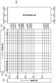
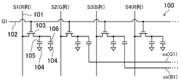
- FIG. 3 is a circuit diagram illustrating a circuit configuration of a main part of the liquid crystal display device 100 of Embodiment 1.
- FIG. FIG. 3 is a block diagram illustrating a connection relationship of each drive circuit according to the first embodiment.
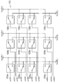
- 2 is a circuit diagram illustrating a configuration of an auxiliary capacitance driving circuit 123 according to the first embodiment.
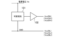
- FIG. 3 is a circuit diagram of a voltage supply circuit to an auxiliary capacity drive circuit 123 of Embodiment 1.
- FIG. 6 is a circuit diagram illustrating a circuit configuration of a main part of a liquid crystal display device 100 according to Embodiment 2.
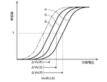
- FIG. 10 is a graph showing the relationship between the voltage and the transmittance of the pixel electrode 105 of Embodiment 2.
- FIG. 6 is a circuit diagram illustrating a circuit configuration of a main part of a liquid crystal display device 100 according to a third embodiment.
- 10 is a graph showing the relationship between the voltage of the pixel electrode 105 and the transmittance of the fourth embodiment.
- FIG. 10 is a circuit diagram of a voltage supply circuit to an auxiliary capacitance drive circuit 123 of Embodiment 5.
- Embodiment 1 (Configuration of the liquid crystal display device 100)
- a liquid crystal display device 100 in which liquid crystal is sealed between a pair of glass substrates includes a source line connected to a source line driving circuit 121 or a gate line driving circuit 122, as shown in FIGS. 101 (S1 to Sn) and gate lines 102 (G1 to Gm) are provided.
- a switching element 103 is provided at the intersection of each source line 101 and each gate line 102. The source electrode and the gate electrode of the switching element 103 are connected to the source line 101 or the gate line 102, respectively.
- the pixel electrode 105 is connected to the drain electrode of the switching element 103.
- the pixel electrode 105 is disposed corresponding to the red (R), green (G), and blue (B) regions in a color filter (not shown).
- a liquid crystal capacitor is formed between the pixel electrode 105 and the counter electrode 104 provided opposite thereto, and a voltage corresponding to the electric charge accumulated in the liquid crystal capacitor is applied to the liquid crystal. Brightness is displayed according to the voltage.
- the drain electrode of the switching element 103 is connected to an electrode on one end side of the auxiliary capacitor 106 that assists the accumulation of electric charges by the liquid crystal capacitor.
- the electrode on the other end side of the auxiliary capacitor 106 is connected to a separate other end side voltage wiring cs (R1... G1... B1...) For each display line and for each color pixel. More specifically, for example, the other end side electrode of the auxiliary capacitor 106 in the red, green, and blue pixels corresponding to the gate line 102 (G1) is connected to the other end side voltage wiring cs (R1, G1, B1). Yes. Similarly, the other end side electrodes of the auxiliary capacitors 106 in the red, green, and blue pixels corresponding to the gate line 102 (G2) are connected to the other end side voltage wiring cs (R2, G2, B2), respectively. .
- the other end side voltage wirings cs (R1,..., G1,..., B1...) are connected to the auxiliary capacitance driving circuit 123.
- the auxiliary capacity driving circuit 123 is provided with changeover switches 123a to 123c.
- the change-over switches 123a to 123c are respectively connected to the other end side voltage wirings cs (R1,..., G1,..., B1...)
- the other end side high voltage Vcs (RH, GH, BH) is supplied via a voltage follower 132, for example, as shown in FIG. It is like that.
- the other end side low voltage Vcs (RL, GL, BL) may be supplied for each color pixel in the same manner. However, in the example of FIG. It has become so.
- the gate line 102 (G1) is set to the H (High) level by the gate line driving circuit 122
- the switching element 103 corresponding to the first display line is turned on. Therefore, when the image signal voltage of each pixel is output from the source line driving circuit 121, the image signal voltage is supplied from the source line 101 (S1 to Sn) via the switching element 103 to the pixel electrode 105 and the auxiliary capacitor 106. Applied to one end side electrode. At this time, the other end side low voltage Vcs (RL, GL, BL) is applied to the other end side electrode of the auxiliary capacitor 106 via the other end side voltage wiring cs (R1, G1, B1).
- the switching element 103 corresponding to the first display line is turned off, and the pixel electrode 105 and the auxiliary capacitor 106 are connected to the source line 101. Detached from. Thereafter, the voltage applied to the other end side voltage wiring cs (R1, G1, B1) is switched to the other end side high voltage Vcs (RH, GH, BH). As a result, the voltage of the pixel electrode 105 changes, which will be described in detail later.
- the gate lines 102 are sequentially set to the H level, and the other end side voltage wiring cs (R2... G2... B2.
- the low side voltage Vcs (RL, GL, BL)
- an image signal voltage is applied from the source line 101 to the pixel electrode 105 and one end side electrode of the auxiliary capacitor 106, and the gate line 102 (G2).
- the voltage applied to the other end side voltage wiring cs (R2... G2... B2...) Is switched to the other end side high voltage Vcs (RH, GH, BH).
- the voltage applied to the other end side voltage wiring cs (R, G, B) is changed to the other end.
- the voltage of the pixel electrode 105 is From Vlc (R, G, B) If it changes to Vlc (R, G, B) + ⁇ Vlc (R, G, B), then ⁇ Vlc (R, G, B) is as follows.
- ⁇ Vlc (R, G, B) ⁇ Vcs (R, G, B) ⁇ Ccs / (Clc + Ccs) here, ⁇ Vcs (R, G, B): difference between the other end side high and low voltages Vcs (RH, GH, BH), Vcs (RL, GL, BL) Clc: liquid crystal capacitance Ccs between the pixel electrode 105 and the counter electrode 104: This is the size of the auxiliary capacitor 106.
- the image signal voltage is positive is described as an example for convenience of explanation.
- the image signal voltage is negative with respect to the negative image signal voltage.
- the same effect can be obtained. That is, when a positive image signal voltage is applied to the pixel electrode, if the voltage applied to the other end side voltage wiring cs (R, G, B) is switched in the positive direction, the pixel as described above.
- the voltage of the electrode 105 fluctuates in the positive direction, and when a negative image signal voltage is applied to the pixel electrode, the voltage applied to the other end side voltage wiring cs (R, G, B) is negative. If switched, the voltage of the pixel electrode 105 fluctuates in the negative direction. That is, the absolute value of the voltage of the pixel electrode 105 with respect to the counter electrode 104 can be changed in the same way regardless of the polarity.
- an image signal voltage having a positive polarity relative to the counter electrode 104 is sourced in an Nth (N is a natural number) frame (for example, an odd-numbered frame).
- N is a natural number
- the voltage applied to the other end side voltage wiring cs (R, G, B) is the other end side low voltage.
- Vcs (RH, GH, BH) is switched to the other end side low voltage Vcs (RL, GL, BL).
- the other end side voltage wiring cs (R The voltage applied to the odd number, G odd number, and B odd number) is switched from the other end side high voltage Vcs (RH, GH, BH) to the other end side low voltage Vcs (RL, GL, BL).
- the voltage applied to the other end side voltage wiring cs (R even number, G even number, B even number) is changed from the other end side low voltage Vcs (RL, GL, BL) to the other end side high voltage Vcs (RH, GH, BH). Can be switched to.
- the other-end-side low voltage Vcs (RL, GL, BL) and the other-end-side high voltage Vcs (RH, GH, BH) corresponding to the positive and negative image signal voltages are the same.
- the voltage may be a voltage symmetrical to the voltage of the counter electrode.
- Embodiment 2 The voltage of the other end side electrode of the auxiliary capacitor 106 does not necessarily have to be switched for all colors. Specifically, for example, as shown in FIG. 7, for the red pixel, the other end side electrode of the auxiliary capacitor 106 is connected to the counter electrode 104 to fix the voltage, and only the green and blue pixels have the auxiliary capacitor 106. The other end side electrode may be connected to the other end side voltage wiring cs (G, B) so that the voltage can be switched in the same manner as in the first embodiment.
- G, B other end side voltage wiring cs
- the characteristics of the applied voltage to the pixel electrode 105 and the transmittance (and hence the luminance of each color) for red, green, and blue can be relatively adjusted. For example, as shown in FIG. These characteristics can be adjusted to substantially match the characteristics of red.
- the number of voltage wirings on the other end side can be reduced, so that the aperture ratio can be easily increased and the circuit scale of the auxiliary capacitor driving circuit 123 and the like can be reduced. You can also.
- the absolute luminance of each color can be obtained by uniformly increasing or decreasing the image signal voltage of each color applied from the source line driving circuit 121 or increasing or decreasing the voltage of the counter electrode 104. May also be adjusted.
- Embodiment 3 The voltage of the electrode on the other end of the auxiliary capacitor 106 may be switched in common for a plurality of colors. That is, for example, when the characteristics of the voltage applied to the pixel electrode 105 and the transmittance are the same or similar for red and green, as shown in FIG. The same voltage may be applied by connecting the end electrodes to the common other end side voltage wiring cs (RG1). Even in such a case, since the number of the other-end side voltage wirings can be reduced, the aperture ratio can be easily increased, and the circuit scale of the auxiliary capacitance driving circuit 123 and the like can be reduced.
- liquid crystal display device 100 for example, a TN (Twisted Nematic) type in which polarizing plates are arranged in parallel Nicols, or a VA (Vertical Alignment) in which polarizing plates are arranged in crossed Nicols.
- TN Transmission Nematic
- VA Very Alignment
- the present invention is not limited to this.
- a normally white liquid crystal display device as shown in FIG. 10 can provide the same effect. That is, in the case of the characteristics of applied voltage and transmittance to the pixel electrode 105 as shown in FIG.
- the magnitude relationship of the voltage may be set according to the wavelength transmittance characteristic of the color filter, and is not necessarily limited to the above.
- Embodiment 5 The other-end high voltage Vcs (RH, GH, BH) is not limited to being fixedly set by the variable resistor 131 as shown in FIG. 4, but may be variably set by software or the like. Specifically, for example, as shown in FIG. 11, the setting data is received by serial communication or the like and held in the register 141, and a voltage corresponding to the held setting data is generated by the D / A converter 142 to generate a voltage. You may make it supply via the follower 132. FIG. In the case of such a configuration, it is possible to easily adjust the characteristics flexibly when using the liquid crystal display device 100, or to compensate for changes in characteristics over time.
- auxiliary capacitor driving circuit 123 and the like are connected to the liquid crystal display device 100.
- the present invention is not limited to this, and these driving circuits and the like are provided in the liquid crystal display device 100 and modularized. Etc.
- the other end side high voltage Vcs (RH, GH, BH) is made different from each other for red, green, and blue, while the other end side low voltage Vcs (RL, GL, BL) is changed.
- the ground voltage is equally set
- the present invention is not limited to this, and as a result, the other-end high / low voltages Vcs (RH, GH, BH), Vcs (so that the voltage of the pixel electrode 105 becomes a desired voltage.
- RL, GL, BL) or a difference ⁇ Vcs (R, G, B) may be set.
- the voltage of the other end side voltage wiring cs (R3, G3, B3) is the same as that of the other end side low voltage Vcs (RL, GL,
- the present invention is not limited to this, and the other end side low voltage Vcs (RL, GL, BL) is set only near the time when the gate line 102 (G3) is at the H level. It may be.
- the voltage applied to the other end side voltage wiring cs (R3, G3, B3) is
- the other end side low voltage Vcs (RL, GL, BL) is switched to the other end side high voltage Vcs (RH, GH, BH)
- the gate line 102 (G3) is set to the H level again in the next frame.
- the voltage may be returned to the low voltage Vcs (RL, GL, BL) on the other end side immediately before the gate line 102 (G3) is set to the H level.
- the other-end voltage wiring cs (R, G, B) is not limited to be provided corresponding to each scanning line, and may be shared by two or more scanning lines. Specifically, for example, in FIG. 5, the other end side voltage wiring cs (R1, G1, B1) is omitted, and the voltage supplied from the other end side voltage wiring cs (R2, G2, B2) is one line. You may make it apply to the other end side electrode of the auxiliary capacity
- the present invention is useful for a liquid crystal display device that displays a color image.
Landscapes
- Engineering & Computer Science (AREA)
- Chemical & Material Sciences (AREA)
- Crystallography & Structural Chemistry (AREA)
- Physics & Mathematics (AREA)
- Computer Hardware Design (AREA)
- General Physics & Mathematics (AREA)
- Theoretical Computer Science (AREA)
- Liquid Crystal Display Device Control (AREA)
- Liquid Crystal (AREA)
- Control Of Indicators Other Than Cathode Ray Tubes (AREA)
Abstract
各色ごとの画素電極への印加電圧と透過率の特性を調整可能にするため、補助容量106の一端側の電極はスイッチング素子103のドレイン電極に接続されている。補助容量106の他端側の電極は、表示ラインごと、および各色の画素ごとに、それぞれ別個の他端側電圧配線cs(R1…、G1…、B1…)に接続されている。スイッチング素子103がオフ状態になった後に、各他端側電圧配線の電圧を切り替えることによって、赤色、緑色、青色の画素電極105の電圧が個別に変化するように設定できる。
Description
本発明は、カラー画像を表示する液晶表示装置に関するものである。
カラー画像を表示する液晶表示装置では、表示画像に応じた画像信号電圧を画素電極に印加し、例えば赤(R)、緑(G)、青(B)の3色のカラーフィルタを透過した光を合成することによって、表示が行われる。ここで、上記カラーフィルタの透過率が色ごとに異なると、各色の画素電極に同一の画像信号電圧を印加しても各色の輝度は同一にならない。そこで、例えば液晶容量と並列に接続される補助容量の大きさを各色ごとに異ならせるなどして、画素電極への印加電圧と各色の透過率の特性を調整する技術が知られている(例えば、特許文献1、2参照)。
上記のように液晶容量と並列に接続される補助容量の大きさ等を各色ごとに異ならせれば、画素電極への印加電圧と透過率の特性を調整することができる。しかし、その調整は、全ての液晶パネルに対して一律に行われるもので、例えば印加電圧と透過率の特性が液晶パネルごとにばらつく場合には、液晶パネルごとに調整することができない。
したがって、全ての液晶パネルについて、同一の画像信号電圧に対して各色の輝度が同一になるようにすることなどは困難であるという問題点を有していた。
本発明は、かかる点に鑑みてなされたものであり、その目的は、各色ごとの画素電極への印加電圧と透過率の特性を容易に調整できるようにすることにある。
第1の発明は、
複数種類の色ごとに設けられた画素電極と、
上記画素電極に対向して設けられた対向電極と、
各画素電極に一端が接続された補助容量とを有し、
上記画素電極と対向電極との間の電圧に応じた輝度の表示が行われる液晶表示装置であって、
上記補助容量の他端に、各色ごとに異なる他端側電圧を印加し得る他端側電圧配線が接続されていることを特徴とする。
複数種類の色ごとに設けられた画素電極と、
上記画素電極に対向して設けられた対向電極と、
各画素電極に一端が接続された補助容量とを有し、
上記画素電極と対向電極との間の電圧に応じた輝度の表示が行われる液晶表示装置であって、
上記補助容量の他端に、各色ごとに異なる他端側電圧を印加し得る他端側電圧配線が接続されていることを特徴とする。
これにより、補助容量の他端に所定の他端側電圧を印加すると、画素電極の電圧が変化する。そして、上記印加する他端側電圧は、各色ごとに異ならせることができる。そこで、例えば複数種類の色の画素電極に同一の画像信号電圧が印加されたとしても、その画素電極の電圧を各色ごとに異ならせるように変化させることができる。したがって、各色ごとの画素電極への印加電圧と透過率の特性を容易に調整できる。
第2の発明は、
第1の発明の液晶表示装置であって、
上記他端側電圧配線が、複数種類の色のうちの一部だけに対して設けられていることを特徴とする。
第1の発明の液晶表示装置であって、
上記他端側電圧配線が、複数種類の色のうちの一部だけに対して設けられていることを特徴とする。
このように構成される場合でも、他端側電圧配線が設けられていない色と設けられている色とについての相対関係においては、各色ごとの画素電極への印加電圧と透過率の特性を容易に調整できる。しかも、他端側電圧配線の本数を少なく抑えることができるので、開口率を大きく保つことが容易にできる。
第3の発明は、
第1の発明の液晶表示装置であって、
上記他端側電圧配線が、複数種類の色のうちの一部の複数の色に対して共通に設けられていることを特徴とする。
第1の発明の液晶表示装置であって、
上記他端側電圧配線が、複数種類の色のうちの一部の複数の色に対して共通に設けられていることを特徴とする。
これにより、画素電極への印加電圧と透過率の特性が同様である色については、画素電極の電圧を同じように変化させればよいので、適切な調整を可能にしつつ、やはり、他端側電圧配線の本数を少なく抑えて、開口率を大きく保つことが容易にできる。
第4の発明は、
第1から第3の発明のうち何れか1つの発明の液晶表示装置であって、
さらに、画素電極への画像信号電圧の印加中と、その印加が終了した後とで、互いに異なる他端側電圧を切り替えて上記他端側電圧配線に印加する駆動回路を備え、
上記互いに異なる他端側電圧の少なくとも一方が各色ごとに異なることを特徴とする。
第1から第3の発明のうち何れか1つの発明の液晶表示装置であって、
さらに、画素電極への画像信号電圧の印加中と、その印加が終了した後とで、互いに異なる他端側電圧を切り替えて上記他端側電圧配線に印加する駆動回路を備え、
上記互いに異なる他端側電圧の少なくとも一方が各色ごとに異なることを特徴とする。
このような駆動回路を備えることによって、上記で説明したような各色ごとの画素電極への印加電圧と透過率の特性の調整を容易にできる。
第5の発明は、
第4の発明の液晶表示装置であって、
上記他端側電圧が設定可能に構成されていることを特徴とする。
第4の発明の液晶表示装置であって、
上記他端側電圧が設定可能に構成されていることを特徴とする。
これにより、例えば、液晶表示装置の出荷時に特性のばらつきを補償することなどが容易にできる。
第6の発明は、
第5の発明の液晶表示装置であって、
上記他端側電圧は、制御信号に応じて可変に設定されるように構成されていることを特徴とする。
第5の発明の液晶表示装置であって、
上記他端側電圧は、制御信号に応じて可変に設定されるように構成されていることを特徴とする。
これにより、例えば、液晶表示装置の使用時に柔軟に特性を調整したり、特性の経時変化を補償したりすることなどが容易にできる。
第7の発明は、
第4から第6の発明のうち何れか1つの発明の液晶表示装置であって、
各表示ラインに対応する画素電極についての上記他端側電圧における互いに異なる他端側電圧への切り替えが、各表示ラインの走査に対応して、順次行われるように構成されていることを特徴とする。
第4から第6の発明のうち何れか1つの発明の液晶表示装置であって、
各表示ラインに対応する画素電極についての上記他端側電圧における互いに異なる他端側電圧への切り替えが、各表示ラインの走査に対応して、順次行われるように構成されていることを特徴とする。
これにより、各表示ラインごとの表示を適切な特性で行わせることが容易にできる。
第8の発明は、
第4から第7の発明のうち何れか1つの発明の液晶表示装置であって、
表示ラインまたはフレームごとに、対向電極に対して極性が交互に反転する画像信号電圧が画素電極に印加されるように構成されるとともに、
上記駆動回路は、画素電極への、対向電極に対して正極性の画像信号電圧の印加が終了した後に、上記印加中よりも高い他端側電圧を他端側電圧配線に印加する一方、画素電極への、対向電極に対して負極性の画像信号電圧の印加が終了した後に、上記印加中よりも低い他端側電圧を他端側電圧配線に印加するように構成されていることを特徴とする。
第4から第7の発明のうち何れか1つの発明の液晶表示装置であって、
表示ラインまたはフレームごとに、対向電極に対して極性が交互に反転する画像信号電圧が画素電極に印加されるように構成されるとともに、
上記駆動回路は、画素電極への、対向電極に対して正極性の画像信号電圧の印加が終了した後に、上記印加中よりも高い他端側電圧を他端側電圧配線に印加する一方、画素電極への、対向電極に対して負極性の画像信号電圧の印加が終了した後に、上記印加中よりも低い他端側電圧を他端側電圧配線に印加するように構成されていることを特徴とする。
これにより、いわゆるライン反転駆動やフレーム反転駆動などが行われる液晶表示装置に対して、各色ごとの画素電極への印加電圧と透過率の特性を容易に調整できる。
第9の発明は、
第1から第8の発明のうち何れか1つの発明の液晶表示装置であって、
上記他端側電圧配線が、2本以上の表示ラインにおける同一色の画素に対して共通に設けられていることを特徴とする。
第1から第8の発明のうち何れか1つの発明の液晶表示装置であって、
上記他端側電圧配線が、2本以上の表示ラインにおける同一色の画素に対して共通に設けられていることを特徴とする。
これにより、他端側電圧配線の本数を少なく抑えることができるので、開口率を大きく保つことが容易にできる。
第10の発明は、
第1から第3の発明のうち何れか1つの発明の液晶表示装置の上記他端側電圧配線に上記他端側電圧を印加する駆動回路であって、
画素電極への画像信号電圧の印加中と、その印加が終了した後とで、互いに異なる他端側電圧を切り替えて上記他端側電圧配線に印加するとともに、
上記互いに異なる他端側電圧の少なくとも一方が各色ごとに異なるように構成されていることを特徴とする。
第1から第3の発明のうち何れか1つの発明の液晶表示装置の上記他端側電圧配線に上記他端側電圧を印加する駆動回路であって、
画素電極への画像信号電圧の印加中と、その印加が終了した後とで、互いに異なる他端側電圧を切り替えて上記他端側電圧配線に印加するとともに、
上記互いに異なる他端側電圧の少なくとも一方が各色ごとに異なるように構成されていることを特徴とする。
これにより、第1の発明の液晶表示装置に対して、上記で説明したような各色ごとの画素電極への印加電圧と透過率の特性を容易に調整できる。
本発明によれば、各色ごとの画素電極への印加電圧と透過率の特性を容易に調整できる。
以下、本発明の実施形態を図面に基づいて詳細に説明する。なお、以下の各実施形態において、他の実施形態と同様の機能を有する構成要素については同一の符号を付して説明を省略する。
《実施形態1》
(液晶表示装置100の構成)
1対のガラス基板間に液晶が封入されて成る液晶表示装置100には、例えば図1、図2に示すように、それぞれソースライン駆動回路121、またはゲートライン駆動回路122に接続されたソースライン101(S1~Sn)、およびゲートライン102(G1~Gm)が設けられている。各ソースライン101と各ゲートライン102との交差位置には、スイッチング素子103が設けられている。このスイッチング素子103のソース電極およびゲート電極は、それぞれソースライン101またはゲートライン102に接続されている。
(液晶表示装置100の構成)
1対のガラス基板間に液晶が封入されて成る液晶表示装置100には、例えば図1、図2に示すように、それぞれソースライン駆動回路121、またはゲートライン駆動回路122に接続されたソースライン101(S1~Sn)、およびゲートライン102(G1~Gm)が設けられている。各ソースライン101と各ゲートライン102との交差位置には、スイッチング素子103が設けられている。このスイッチング素子103のソース電極およびゲート電極は、それぞれソースライン101またはゲートライン102に接続されている。
上記スイッチング素子103のドレイン電極には、画素電極105が接続されている。上記画素電極105は、図示しないカラーフィルタにおける赤色(R)、緑色(G)、青色(B)の領域に対応して配置されている。画素電極105と、これに対向して設けられた対向電極104との間には液晶容量が形成され、上記液晶容量に蓄積される電荷に応じた電圧が液晶に印加されることによって、その印加電圧に応じた輝度の表示が行われるようになっている。
スイッチング素子103のドレイン電極には、また、液晶容量による電荷の蓄積を補助する補助容量106の一端側の電極が接続されている。補助容量106の他端側の電極は、表示ラインごと、および各色の画素ごとに、それぞれ別個の他端側電圧配線cs(R1…、G1…、B1…)に接続されている。より詳しくは、例えば、ゲートライン102(G1)に対応する赤色、緑色、青色画素における補助容量106の他端側電極は、それぞれ他端側電圧配線cs(R1、G1、B1)に接続されている。また、同様に、ゲートライン102(G2)に対応する赤色、緑色、青色画素における補助容量106の他端側電極は、それぞれ他端側電圧配線cs(R2、G2、B2)に接続されている。
各他端側電圧配線cs(R1…、G1…、B1…)は、補助容量駆動回路123に接続されている。補助容量駆動回路123には、例えば図3に示すように、切り替えスイッチ123a~123cが設けられている。上記切り替えスイッチ123a~123cは、それぞれ、赤色、緑色、または青色画素に対応する他端側電圧配線cs(R1…、G1…、B1…)に、所定の他端側高電圧Vcs(RH、GH、BH)、または他端側低電圧Vcs(RL、GL、BL)を選択的に印加するようになっている。
上記他端側高電圧Vcs(RH、GH、BH)は、例えば図4に示すように、基準となる電源電圧Vaを可変抵抗131によって分圧した電圧が、ボルテージフォロワ132を介して供給されるようになっている。また、上記他端側低電圧Vcs(RL、GL、BL)は、同様にして各色の画素ごとに供給されるようにしてもよいが、同図の例では、共通に接地電圧GNDが供給されるようになっている。
(液晶表示装置100の動作)
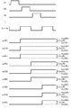
上記のように構成された液晶表示装置100の動作について、図5に基づいて説明する。
上記のように構成された液晶表示装置100の動作について、図5に基づいて説明する。
まず、ゲートライン駆動回路122によってゲートライン102(G1)がH(High)レベルにされると、1ライン目の表示ラインに対応するスイッチング素子103がオン状態になる。そこで、ソースライン駆動回路121から各画素の画像信号電圧が出力されると、その画像信号電圧がソースライン101(S1~Sn)からスイッチング素子103を介して、画素電極105と、補助容量106の一端側電極とに印加される。このとき、補助容量106の他端側電極には、他端側電圧配線cs(R1、G1、B1)を介して他端側低電圧Vcs(RL、GL、BL)が印加される。
次に、ゲートライン102(G1)がL(Low)レベルにされると、1ライン目の表示ラインに対応するスイッチング素子103がオフ状態になり、画素電極105、および補助容量106はソースライン101から切り離される。その後、他端側電圧配線cs(R1、G1、B1)に印加される電圧が他端側高電圧Vcs(RH、GH、BH)に切り替えられる。これによって、画素電極105の電圧が変化するが、この点については後に詳しく説明する。
以下、2ライン目以降の表示ラインについても、同様に、ゲートライン102(G2…)が順次Hレベルにされるとともに、他端側電圧配線cs(R2…、G2…、B2…)に他端側低電圧Vcs(RL、GL、BL)が印加された状態で、画像信号電圧がソースライン101から画素電極105と補助容量106の一端側電極とに印加され、ゲートライン102(G2…)がLレベルにされた後、他端側電圧配線cs(R2…、G2…、B2…)に印加される電圧が他端側高電圧Vcs(RH、GH、BH)に切り替えられる。
(画素電極105の電圧について)
上記のような動作が行われる場合の画素電極105の電圧の変化について説明する。以下の説明では、便宜上、表示ラインの区別を省略して、例えば他端側電圧配線cs(R1)等を単にcs(R)等と表記する。
上記のような動作が行われる場合の画素電極105の電圧の変化について説明する。以下の説明では、便宜上、表示ラインの区別を省略して、例えば他端側電圧配線cs(R1)等を単にcs(R)等と表記する。
ソースライン101を介して画素電極105に例えば画像信号電圧Vlc(R、G、B)が印加された後に、他端側電圧配線cs(R、G、B)に印加される電圧が、他端側低電圧Vcs(RL、GL、BL)から他端側高電圧Vcs(RH、GH、BH)に切り替えられることによって、画素電極105の電圧が、
Vlc(R、G、B)から、
Vlc(R、G、B)+ΔVlc(R、G、B)に変化するとすると、上記ΔVlc(R、G、B)は次のようになる。
Vlc(R、G、B)から、
Vlc(R、G、B)+ΔVlc(R、G、B)に変化するとすると、上記ΔVlc(R、G、B)は次のようになる。
ΔVlc(R、G、B)=ΔVcs(R、G、B)×Ccs/(Clc+Ccs)
ここで、
ΔVcs(R、G、B):他端側高低電圧Vcs(RH、GH、BH)、Vcs(RL、GL、BL)の差
Clc :画素電極105と対向電極104との間の液晶容量
Ccs :補助容量106の大きさ
である。
ここで、
ΔVcs(R、G、B):他端側高低電圧Vcs(RH、GH、BH)、Vcs(RL、GL、BL)の差
Clc :画素電極105と対向電極104との間の液晶容量
Ccs :補助容量106の大きさ
である。
そこで、他端側高低電圧Vcs(RH、GH、BH)、Vcs(RL、GL、BL)を適切に設定すると、例えば図6に示すように、ソースライン101から各色の画素電極105に印加する画像信号電圧Vlc(R、G、B)が同一である場合に、画素電極105の電圧がΔVlc(R、G、B)だけ変化して、その結果、同一の透過率Tとなるようにすることができる。すなわち、各色についての画素電極105への印加電圧と透過率の特性を、実質的に、同図に2点鎖線で示すような特性に調整することが容易にできる。しかも、そのような調整は液晶表示装置100ごとに行えるので、例えば液晶パネルごとに特性のばらつきがある場合などでも、そのばらつきの影響を解消または低減することも容易にできる。
なお、上記では、説明の便宜上、画像信号電圧が正極性である場合を例に挙げて説明したが、通常の液晶表示装置のように交流駆動が行われる場合、負極性の画像信号電圧に対しても同様の効果を得ることができる。すなわち、画素電極に正極性の画像信号電圧が印加される場合には、他端側電圧配線cs(R、G、B)に印加される電圧が正方向に切り替えられれば、上記のように画素電極105の電圧は正方向に変動し、画素電極に負極性の画像信号電圧が印加される場合には、他端側電圧配線cs(R、G、B)に印加される電圧が負方向に切り替えられれば、画素電極105の電圧は負方向に変動する。すなわち、対向電極104に対する画素電極105の電圧の絶対値を何れの極性でも同じように変化させることができる。
具体的には、例えば、いわゆるフレーム反転駆動が行われる場合、第N(Nは自然数)フレーム(例えば奇数番目のフレーム)で、対向電極104に対して相対的に正極性の画像信号電圧がソースライン101(S1~Sn)に供給される場合には、上記および図5に示したように、他端側電圧配線cs(R、G、B)に印加される電圧が、他端側低電圧Vcs(RL、GL、BL)から他端側高電圧Vcs(RH、GH、BH)に切り替えられると、画素電極105の電圧は正方向に変動する。これに対して、次の第N+1フレーム(例えば偶数番目のフレーム)で、対向電極104に対して相対的に負極性の画像信号電圧がソースライン101(S1~Sn)に供給される場合には、他端側電圧配線cs(R、G、B)に印加される電圧が、他端側高電圧Vcs(RH、GH、BH)から他端側低電圧Vcs(RL、GL、BL)に切り替えられると、画素電極105の電圧は負方向に変動する。すなわち、対向電極104に対する画素電極105の電圧の絶対値が、何れの極性でも同じように大きくなるように変化させることができる。
また、例えば、いわゆるライン反転駆動が行われる場合には、第Nフレームにおいて、奇数ライン(走査ライン)の各画素(画素電極105)に正極性の画像信号電圧、偶数ラインの各画素に負極性の画像信号電圧が印加されるとすると、奇数ラインの他端側電圧配線cs(R奇数、G奇数、B奇数)に印加される電圧は、他端側低電圧Vcs(RL、GL、BL)から他端側高電圧Vcs(RH、GH、BH)に切り替えられる一方、偶数ラインの他端側電圧配線cs(R偶数、G偶数、B偶数)に印加される電圧は、他端側高電圧Vcs(RH、GH、BH)から他端側低電圧Vcs(RL、GL、BL)に切り替えられる。また、第N+1フレームにおいて、奇数ラインの各画素に負極性の画像信号電圧、偶数ラインの各画素に正極性の画像信号電圧が印加されるとすると、奇数ラインの他端側電圧配線cs(R奇数、G奇数、B奇数)に印加される電圧は、他端側高電圧Vcs(RH、GH、BH)から他端側低電圧Vcs(RL、GL、BL)に切り替えられる一方、偶数ラインの他端側電圧配線cs(R偶数、G偶数、B偶数)に印加される電圧は、他端側低電圧Vcs(RL、GL、BL)から他端側高電圧Vcs(RH、GH、BH)に切り替えられる。
さらに、例えば各走査ラインにおける互いに隣り合う画素ごとに逆極性の画像信号電圧が印加される、いわゆるドット反転駆動等が行われる場合にも、各色と画像信号電圧の極性との組み合わせごとに他端側電圧配線を設ければ、同様に各色についての画素電極への印加電圧と透過率の特性を調整することができる。
ここで、上記のような場合に、正負の画像信号電圧に対応する他端側低電圧Vcs(RL、GL、BL)、他端側高電圧Vcs(RH、GH、BH)は、それぞれ同一の電圧であってもよく、また、例えば対向電極の電圧に対して対称な電圧などであってもよい。
《実施形態2》
補助容量106の他端側電極の電圧は、必ずしも全ての色について切り替えなくてもよい。具体的には、例えば図7に示すように、赤色画素については、補助容量106の他端側電極を対向電極104に接続して電圧を固定し、緑色、青色画素についてだけ、補助容量106の他端側電極を他端側電圧配線cs(G、B)に接続して、その電圧を実施形態1と同様に切り替えられるようにしてもよい。これによって、赤色、緑色、および青色についての画素電極105への印加電圧と透過率の特性(したがって各色の輝度)を相対的に調整できるので、例えば図8に示すように、緑色、および青色についての特性を、実質的に、赤色についての特性に合わせるように調整することなどができる。
補助容量106の他端側電極の電圧は、必ずしも全ての色について切り替えなくてもよい。具体的には、例えば図7に示すように、赤色画素については、補助容量106の他端側電極を対向電極104に接続して電圧を固定し、緑色、青色画素についてだけ、補助容量106の他端側電極を他端側電圧配線cs(G、B)に接続して、その電圧を実施形態1と同様に切り替えられるようにしてもよい。これによって、赤色、緑色、および青色についての画素電極105への印加電圧と透過率の特性(したがって各色の輝度)を相対的に調整できるので、例えば図8に示すように、緑色、および青色についての特性を、実質的に、赤色についての特性に合わせるように調整することなどができる。
上記のように構成する場合には、他端側電圧配線の本数を減らすことができるので、開口率を大きくすることが容易にできるとともに、補助容量駆動回路123等の回路規模を低減することなどもできる。
なお、上記のように構成する場合でも、ソースライン駆動回路121から印加される各色の画像信号電圧を一律に増減させたり、対向電極104の電圧を増減させたりして、各色の絶対的な輝度も調整されるようにしてもよい。
《実施形態3》
補助容量106の他端側電極の電圧を、複数の色について共通に切り替えるようにしてもよい。すなわち、例えば赤色と緑色についての画素電極105への印加電圧と透過率の特性が一致し、または似通っている場合には、図9に示すように、赤色、緑色画素についての補助容量106の他端側電極をそれぞれ共通の他端側電圧配線cs(RG1…)に接続して、同一の電圧が印加されるようにしてもよい。このような場合にも、他端側電圧配線の本数を減らすことができるので、開口率を大きくすることが容易にできるとともに、補助容量駆動回路123等の回路規模を低減することなどもできる。
補助容量106の他端側電極の電圧を、複数の色について共通に切り替えるようにしてもよい。すなわち、例えば赤色と緑色についての画素電極105への印加電圧と透過率の特性が一致し、または似通っている場合には、図9に示すように、赤色、緑色画素についての補助容量106の他端側電極をそれぞれ共通の他端側電圧配線cs(RG1…)に接続して、同一の電圧が印加されるようにしてもよい。このような場合にも、他端側電圧配線の本数を減らすことができるので、開口率を大きくすることが容易にできるとともに、補助容量駆動回路123等の回路規模を低減することなどもできる。
《実施形態4》
上記各実施形態においては、ノーマリブラック(図6)の液晶表示装置100(例えば偏光板がパラレルニコル配置されたTN(Twisted Nematic)型、または偏光板がクロスニコル配置されたVA(Vertical Alignment)型など)を例に挙げて説明したが、これに限らず、例えば図10に示すようなノーマリホワイトの液晶表示装置でも同様の効果を得ることができる。すなわち、図6に示したような画素電極105への印加電圧と透過率の特性の場合には、
ΔVlc(R) ≧ ΔVlc(G) ≧ ΔVlc(B)となるようにするために、
ΔVcs(R) ≧ ΔVcs(G) ≧ ΔVcs(B)となるように設定すればよいのに対し、図10に示すような特性の場合には、
ΔVlc(B) ≧ ΔVlc(G) ≧ ΔVlc(R)となるようにするために、
ΔVcs(B) ≧ ΔVcs(G) ≧ ΔVcs(R)となるように設定すればよい。
上記各実施形態においては、ノーマリブラック(図6)の液晶表示装置100(例えば偏光板がパラレルニコル配置されたTN(Twisted Nematic)型、または偏光板がクロスニコル配置されたVA(Vertical Alignment)型など)を例に挙げて説明したが、これに限らず、例えば図10に示すようなノーマリホワイトの液晶表示装置でも同様の効果を得ることができる。すなわち、図6に示したような画素電極105への印加電圧と透過率の特性の場合には、
ΔVlc(R) ≧ ΔVlc(G) ≧ ΔVlc(B)となるようにするために、
ΔVcs(R) ≧ ΔVcs(G) ≧ ΔVcs(B)となるように設定すればよいのに対し、図10に示すような特性の場合には、
ΔVlc(B) ≧ ΔVlc(G) ≧ ΔVlc(R)となるようにするために、
ΔVcs(B) ≧ ΔVcs(G) ≧ ΔVcs(R)となるように設定すればよい。
さらに、上記電圧の大小関係は、カラーフィルタの波長透過率特性等に応じて設定すればよく、必ずしも上記に限るものではない。
《実施形態5》
他端側高電圧Vcs(RH、GH、BH)は、図4に示したように可変抵抗131によって固定的に設定されるのに限らず、ソフトウェア等によって可変に設定できるようにしてもよい。具体的には、例えば図11に示すように、設定データをシリアル通信等により受信してレジスタ141に保持し、保持された設定データに応じた電圧をD/Aコンバータ142で発生して、ボルテージフォロワ132を介して供給するようにしてもよい。このように構成する場合には、液晶表示装置100の使用時に柔軟に特性を調整したり、特性の経時変化を補償したりすることなどが容易にできる。
他端側高電圧Vcs(RH、GH、BH)は、図4に示したように可変抵抗131によって固定的に設定されるのに限らず、ソフトウェア等によって可変に設定できるようにしてもよい。具体的には、例えば図11に示すように、設定データをシリアル通信等により受信してレジスタ141に保持し、保持された設定データに応じた電圧をD/Aコンバータ142で発生して、ボルテージフォロワ132を介して供給するようにしてもよい。このように構成する場合には、液晶表示装置100の使用時に柔軟に特性を調整したり、特性の経時変化を補償したりすることなどが容易にできる。
《その他の変形例》
上記の例では、液晶表示装置100に補助容量駆動回路123等が接続されている例を示したが、これに限らず、これらの駆動回路等が液晶表示装置100に備えられてモジュール化されるなどしてもよい。
上記の例では、液晶表示装置100に補助容量駆動回路123等が接続されている例を示したが、これに限らず、これらの駆動回路等が液晶表示装置100に備えられてモジュール化されるなどしてもよい。
また、例えば実施形態1等では、赤色、緑色、および青色について、他端側高電圧Vcs(RH、GH、BH)を互いに異ならせる一方、他端側低電圧Vcs(RL、GL、BL)を等しく接地電圧にする例を示したが、これに限るものではなく、結果的に画素電極105の電圧が所望の電圧になるような他端側高低電圧Vcs(RH、GH、BH)、Vcs(RL、GL、BL)、またはその差ΔVcs(R、G、B)が設定されるようにすればよい。
また、図5の例では、例えば他端側電圧配線cs(R3、G3、B3)の電圧は、ゲートライン102(G3)がHレベルになる前から他端側低電圧Vcs(RL、GL、BL)にされている例を示したが、これに限らず、ゲートライン102(G3)がHレベルになる間付近でだけ、他端側低電圧Vcs(RL、GL、BL)にされるようにしてもよい。すなわち、例えば、あるフレームでゲートライン102(G3)がHレベルになって画像信号電圧が画素電極に印加された後、他端側電圧配線cs(R3、G3、B3)に印加される電圧が他端側低電圧Vcs(RL、GL、BL)から他端側高電圧Vcs(RH、GH、BH)に切り替えられた状態は、次のフレームでゲートライン102(G3)が再度Hレベルにされる直前まで維持されるように、つまり、ゲートライン102(G3)がHレベルにされる直前に他端側低電圧Vcs(RL、GL、BL)に戻されるようにしてもよい。このように他端側高電圧Vcs(RH、GH、BH)に切り替えられた状態が長くなるほど、画素電極の電圧を変動させる効果をより高めることが容易にできる。もっとも、実施形態1の変形例で説明したような反転駆動が行われる場合には、互いに逆極性の画像信号電圧が交互に画素電極に印加されるので、それぞれの印加が終了するごとに1回、他端側高低電圧Vcs(RH、GH、BH)、Vcs(RL、GL、BL)の切り替えが行われるだけでよい。
また、他端側電圧配線cs(R、G、B)は、各走査ラインに対応して設けられるのに限らず、2本以上の走査ラインについて共用されるようにしてもよい。具体的には、例えば図5において、他端側電圧配線cs(R1、G1、B1)を省略して、他端側電圧配線cs(R2、G2、B2)から供給される電圧が、1ライン目、および2ライン目における補助容量106の他端側電極に印加されるようにしてもよい。この場合、1ライン目の補助容量106の他端側電極に他端側高電圧Vcs(RH、GH、BH)等が印加される時間は例えば1走査期間程度短くなるとすると、画素電極の電圧を変動させる効果は若干減少するが、他端側電圧配線の本数を低減できるので開口率を大きくすることが容易にできる。
また、上記各実施形態や変形例で説明した構成要素は、論理的に可能な範囲で種々組み合わせてもよい。具体的には、例えば、実施形態4で説明したようなノーマリホワイトの液晶表示装置に、他の実施形態で説明した種々の構成を適用することができる。
以上説明したように、本発明は、カラー画像を表示する液晶表示装置について有用である。
100 液晶表示装置
101 ソースライン
102 ゲートライン
103 スイッチング素子
104 対向電極
105 画素電極
106 補助容量
121 ソースライン駆動回路
122 ゲートライン駆動回路
123 補助容量駆動回路
123a 切り替えスイッチ
123b 切り替えスイッチ
123c 切り替えスイッチ
131 可変抵抗
132 ボルテージフォロワ
141 レジスタ
142 D/Aコンバータ
cs(R、G、B) 他端側電圧配線
101 ソースライン
102 ゲートライン
103 スイッチング素子
104 対向電極
105 画素電極
106 補助容量
121 ソースライン駆動回路
122 ゲートライン駆動回路
123 補助容量駆動回路
123a 切り替えスイッチ
123b 切り替えスイッチ
123c 切り替えスイッチ
131 可変抵抗
132 ボルテージフォロワ
141 レジスタ
142 D/Aコンバータ
cs(R、G、B) 他端側電圧配線
Claims (10)
- 複数種類の色ごとに設けられた画素電極と、
上記画素電極に対向して設けられた対向電極と、
各画素電極に一端が接続された補助容量とを有し、
上記画素電極と対向電極との間の電圧に応じた輝度の表示が行われる液晶表示装置であって、
上記補助容量の他端に、各色ごとに異なる他端側電圧を印加し得る他端側電圧配線が接続されていることを特徴とする液晶表示装置。 - 請求項1の液晶表示装置であって、
上記他端側電圧配線が、複数種類の色のうちの一部だけに対して設けられていることを特徴とする液晶表示装置。 - 請求項1の液晶表示装置であって、
上記他端側電圧配線が、複数種類の色のうちの一部の複数の色に対して共通に設けられていることを特徴とする液晶表示装置。 - 請求項1から請求項3のうち何れか1項の液晶表示装置であって、
さらに、画素電極への画像信号電圧の印加中と、その印加が終了した後とで、互いに異なる他端側電圧を切り替えて上記他端側電圧配線に印加する駆動回路を備え、
上記互いに異なる他端側電圧の少なくとも一方が各色ごとに異なることを特徴とする液晶表示装置。 - 請求項4の液晶表示装置であって、
上記他端側電圧が設定可能に構成されていることを特徴とする液晶表示装置。 - 請求項5の液晶表示装置であって、
上記他端側電圧は、制御信号に応じて可変に設定されるように構成されていることを特徴とする液晶表示装置。 - 請求項4から請求項6のうち何れか1項の液晶表示装置であって、
各表示ラインに対応する画素電極についての上記他端側電圧における互いに異なる他端側電圧への切り替えが、各表示ラインの走査に対応して、順次行われるように構成されていることを特徴とする液晶表示装置。 - 請求項4から請求項7のうち何れか1項の液晶表示装置であって、
表示ラインまたはフレームごとに、対向電極に対して極性が交互に反転する画像信号電圧が画素電極に印加されるように構成されるとともに、
上記駆動回路は、画素電極への、対向電極に対して正極性の画像信号電圧の印加が終了した後に、上記印加中よりも高い他端側電圧を他端側電圧配線に印加する一方、画素電極への、対向電極に対して負極性の画像信号電圧の印加が終了した後に、上記印加中よりも低い他端側電圧を他端側電圧配線に印加するように構成されていることを特徴とする液晶表示装置。 - 請求項1から請求項8のうち何れか1項の液晶表示装置であって、
上記他端側電圧配線が、2本以上の表示ラインにおける同一色の画素に対して共通に設けられていることを特徴とする液晶表示装置。 - 請求項1から請求項3のうち何れか1項の液晶表示装置の上記他端側電圧配線に上記他端側電圧を印加する駆動回路であって、
画素電極への画像信号電圧の印加中と、その印加が終了した後とで、互いに異なる他端側電圧を切り替えて上記他端側電圧配線に印加するとともに、
上記互いに異なる他端側電圧の少なくとも一方が各色ごとに異なるように構成されていることを特徴とする液晶表示装置の駆動回路。
Applications Claiming Priority (2)
| Application Number | Priority Date | Filing Date | Title |
|---|---|---|---|
| JP2011-126850 | 2011-06-07 | ||
| JP2011126850 | 2011-06-07 |
Publications (1)
| Publication Number | Publication Date |
|---|---|
| WO2012169160A1 true WO2012169160A1 (ja) | 2012-12-13 |
Family
ID=47295746
Family Applications (1)
| Application Number | Title | Priority Date | Filing Date |
|---|---|---|---|
| PCT/JP2012/003595 Ceased WO2012169160A1 (ja) | 2011-06-07 | 2012-05-31 | 液晶表示装置、および液晶表示装置の駆動回路 |
Country Status (1)
| Country | Link |
|---|---|
| WO (1) | WO2012169160A1 (ja) |
Citations (5)
| Publication number | Priority date | Publication date | Assignee | Title |
|---|---|---|---|---|
| JPH11160731A (ja) * | 1997-11-28 | 1999-06-18 | Nec Corp | アクティブマトリクス型液晶表示装置 |
| JP2006189679A (ja) * | 2005-01-07 | 2006-07-20 | Sharp Corp | 液晶表示装置 |
| JP2009008919A (ja) * | 2007-06-28 | 2009-01-15 | Sharp Corp | 液晶表示装置 |
| JP2009282109A (ja) * | 2008-05-20 | 2009-12-03 | Toshiba Mobile Display Co Ltd | 表示素子 |
| WO2010131395A1 (ja) * | 2009-05-13 | 2010-11-18 | シャープ株式会社 | 液晶表示パネルおよび液晶表示装置 |
-
2012
- 2012-05-31 WO PCT/JP2012/003595 patent/WO2012169160A1/ja not_active Ceased
Patent Citations (5)
| Publication number | Priority date | Publication date | Assignee | Title |
|---|---|---|---|---|
| JPH11160731A (ja) * | 1997-11-28 | 1999-06-18 | Nec Corp | アクティブマトリクス型液晶表示装置 |
| JP2006189679A (ja) * | 2005-01-07 | 2006-07-20 | Sharp Corp | 液晶表示装置 |
| JP2009008919A (ja) * | 2007-06-28 | 2009-01-15 | Sharp Corp | 液晶表示装置 |
| JP2009282109A (ja) * | 2008-05-20 | 2009-12-03 | Toshiba Mobile Display Co Ltd | 表示素子 |
| WO2010131395A1 (ja) * | 2009-05-13 | 2010-11-18 | シャープ株式会社 | 液晶表示パネルおよび液晶表示装置 |
Similar Documents
| Publication | Publication Date | Title |
|---|---|---|
| JP6360892B2 (ja) | アレイ基板及び液晶表示装置 | |
| JP5618397B2 (ja) | 液晶表示装置 | |
| US8878829B2 (en) | Liquid crystal display and common electrode drive circuit thereof | |
| JP4966341B2 (ja) | 液晶ディスプレイ装置 | |
| JP5517822B2 (ja) | 液晶表示装置 | |
| US8330698B2 (en) | LCD output enable signal generating circuits and LCDs comprising the same | |
| JP2005292831A (ja) | 液晶表示装置 | |
| KR20060111262A (ko) | 표시 장치의 구동 장치 | |
| CN106707640B (zh) | 一种液晶显示面板及装置 | |
| US20060170641A1 (en) | Driving apparatus for liquid crystal display and liquid crystal display including the same | |
| CN112394557B (zh) | 一种显示面板及显示装置 | |
| CN101109875A (zh) | 一种tft lcd像素电极结构及驱动电路 | |
| TWI381343B (zh) | 顯示裝置及其閘極驅動器 | |
| JP2008276116A (ja) | 液晶表示装置及び液晶表示装置の駆動方法 | |
| WO2012169160A1 (ja) | 液晶表示装置、および液晶表示装置の駆動回路 | |
| KR101167929B1 (ko) | 수평전계방식 액정표시소자 | |
| KR100885018B1 (ko) | 액정 표시 장치 및 그 구동 방법 | |
| KR20050077573A (ko) | 액정 표시 장치 | |
| KR100984350B1 (ko) | 액정 표시 장치 및 그 구동 방법 | |
| KR100961958B1 (ko) | 액정 표시 장치의 구동 장치 | |
| KR20060077726A (ko) | 표시 장치 | |
| JP2014063029A (ja) | 表示装置 | |
| KR20050037052A (ko) | 액정 표시 장치의 구동 방법 | |
| KR20050047757A (ko) | 액정 표시 장치 | |
| KR20060016924A (ko) | 액정 표시 장치 |
Legal Events
| Date | Code | Title | Description |
|---|---|---|---|
| 121 | Ep: the epo has been informed by wipo that ep was designated in this application |
Ref document number: 12797010 Country of ref document: EP Kind code of ref document: A1 |
|
| NENP | Non-entry into the national phase |
Ref country code: DE |
|
| 122 | Ep: pct application non-entry in european phase |
Ref document number: 12797010 Country of ref document: EP Kind code of ref document: A1 |
|
| NENP | Non-entry into the national phase |
Ref country code: JP |