WO2012165445A1 - 位相差板の製造方法および位相差板 - Google Patents
位相差板の製造方法および位相差板 Download PDFInfo
- Publication number
- WO2012165445A1 WO2012165445A1 PCT/JP2012/063816 JP2012063816W WO2012165445A1 WO 2012165445 A1 WO2012165445 A1 WO 2012165445A1 JP 2012063816 W JP2012063816 W JP 2012063816W WO 2012165445 A1 WO2012165445 A1 WO 2012165445A1
- Authority
- WO
- WIPO (PCT)
- Prior art keywords
- glass substrate
- region
- laser beam
- output
- retardation
- Prior art date
- Legal status (The legal status is an assumption and is not a legal conclusion. Google has not performed a legal analysis and makes no representation as to the accuracy of the status listed.)
- Ceased
Links
Images










Classifications
-
- G—PHYSICS
- G02—OPTICS
- G02B—OPTICAL ELEMENTS, SYSTEMS OR APPARATUS
- G02B5/00—Optical elements other than lenses
- G02B5/30—Polarising elements
- G02B5/3083—Birefringent or phase retarding elements
-
- B—PERFORMING OPERATIONS; TRANSPORTING
- B23—MACHINE TOOLS; METAL-WORKING NOT OTHERWISE PROVIDED FOR
- B23K—SOLDERING OR UNSOLDERING; WELDING; CLADDING OR PLATING BY SOLDERING OR WELDING; CUTTING BY APPLYING HEAT LOCALLY, e.g. FLAME CUTTING; WORKING BY LASER BEAM
- B23K26/00—Working by laser beam, e.g. welding, cutting or boring
- B23K26/50—Working by transmitting the laser beam through or within the workpiece
- B23K26/53—Working by transmitting the laser beam through or within the workpiece for modifying or reforming the material inside the workpiece, e.g. for producing break initiation cracks
Definitions
- the present invention relates to a retardation plate manufacturing method and a retardation plate.
- a retardation plate (for example, a half-wave plate or a quarter-wave plate) capable of controlling the phase and polarization of light is used in various optical devices including a Blu-ray optical pickup device. .
- an organic polymer film having refractive index anisotropy that is, birefringence, quartz which is a uniaxial crystal, and the like have been used.
- Patent Document 1 discloses a method of forming a band-shaped birefringence region in a glass substrate using laser light.
- a belt-like birefringence region can be formed in a glass substrate by irradiating the glass substrate with laser light and scanning it.
- the glass substrate is cut (diced or scribed) so as to cross the band-shaped birefringent region. It is necessary to chip the glass substrate.
- the band-shaped birefringence region is generated due to the tensile stress due to the thermal effect of laser light irradiation.
- the glass substrate is cut so as to cross the birefringent region, there is a possibility that a crack occurs in the cut portion or the glass substrate is broken.
- An object of the present invention is to provide a method for producing a retardation plate in which cracks and cracks are unlikely to occur in a cut part when a glass substrate is diced or scribed to obtain a chipped retardation plate. It is another object of the present invention to provide a phase difference plate with improved strength at the cut portion.
- a method for producing a retardation plate having a birefringent region in and / or on a glass substrate (A) preparing a glass substrate having first and second surfaces; (B) scanning the output-modulated laser beam in the glass substrate and / or on the glass substrate in a first direction parallel to the first or second surface; Forming a birefringent region having a tensile stress portion and a compressive stress portion along the direction of 1; (C) A method for producing a retardation plate is provided, wherein the glass substrate is cut so as to pass through a compressive stress portion of the birefringent region.
- the compressive stress portion of the birefringent region has a first compressive stress portion and a second compressive stress portion along the first direction, and a tensile stress portion of the birefringent region. Has a tensile stress portion between the first and second compressive stress portions;
- the glass substrate is cut at a first cutting position and a second cutting position, the first compressive stress portion is selected as the first cutting position, and a second cutting position
- the second compressive stress portion may be selected.
- the output-modulated laser light has a portion where the laser output increases stepwise and / or a portion where the laser output decreases stepwise with respect to time
- the first compressive stress portion is generated by irradiating a laser beam whose laser output increases stepwise
- / or the second compressive stress portion is a laser whose laser output decreases stepwise. You may generate
- the output-modulated laser beam may have a repetitive waveform with a period ⁇ .
- the output modulated laser light includes a minimum value and a maximum value of a laser output
- One period ⁇ of the output-modulated laser light may have a flat portion with respect to the minimum time and / or a flat portion with respect to the maximum time.
- the minimum value may be a value other than zero.
- the laser beam may be composed of two or more laser beams in which the focal points are arranged in a line.
- a phase difference plate having a birefringent region in and / or on a glass substrate,
- the birefringent region extends along a first direction from a first end surface of the glass substrate to a second end surface;
- a retardation plate is provided in which a variation in retardation distribution in a region having a length of 500 ⁇ m along the first direction is within ⁇ 5%.
- the birefringence region has a variation of retardation distribution within ⁇ 5% in a region having a length of 500 ⁇ m along a second direction perpendicular to the first direction. There may be.
- a retardation plate obtained by dicing or scribing a glass substrate to obtain a chip when a retardation plate obtained by dicing or scribing a glass substrate to obtain a chip is obtained, it is possible to provide a method for producing a retardation plate in which cracks and cracks are unlikely to occur at the cut portion. In addition, it is possible to provide a retardation plate in which the strength of the cut portion is improved.
- FIG. 2 is a schematic top view (a) of a retardation plate according to the present invention and a schematic stress distribution diagram (b) in a birefringence region of the retardation plate. It is the figure which showed schematically an example of the structure of the optical pick-up apparatus.
- FIG. 3 is a graph showing a retardation distribution of a birefringent region in a scanning direction of laser light of the retardation plate of Example 1.
- FIG. 3 is a graph showing a retardation distribution of a birefringent region in a direction perpendicular to the laser beam scanning direction of the retardation plate of Example 1.
- FIG. It is an enlarged view of the part of the flat part Q2 in FIG.
- FIG. 6 It is an enlarged view of the part of the flat part Q5 in FIG. 6 is a graph showing a retardation distribution of a birefringent region in a scanning direction of a laser beam of a retardation plate of Example 2.
- 6 is a graph showing a retardation distribution of a birefringent region in a direction perpendicular to the scanning direction of laser light of the retardation plate of Example 2.
- 6 is a graph showing retardation distribution of a birefringent region in the scanning direction of laser light of the retardation plate of Example 3.
- 6 is a graph showing retardation distribution of a birefringent region in a direction perpendicular to the scanning direction of laser light of the retardation plate of Example 3.
- 6 is a graph showing retardation distribution of a birefringent region in a scanning direction of laser light of a retardation plate of Example 4.
- 6 is a graph showing a retardation distribution of a birefringent region in a direction perpendicular to the laser beam scanning direction of the retardation plate of Example 4.
- FIG. 1 shows a conceptual diagram of a retardation plate manufacturing method described in Patent Document 1.
- a laser beam 2 is irradiated onto a glass substrate 1 through a lens 3.
- the band-shaped birefringent region 4 can be formed in the glass substrate 1.
- the glass substrate 1 having such a birefringent region 4 as a retardation plate product is crossed across the belt-like birefringent region 4 (for example, along the X direction in FIG. 1). It is necessary to cut the substrate 1 (dicing or scribing) to make the glass substrate 1 into chips.
- the band-shaped birefringent region 4 is generated by a tensile stress due to the thermal effect of the irradiation of the laser beam 2, so that the glass substrate 1 crosses the band-shaped birefringent region of the glass substrate 1.
- a crack may generate
- the output of the laser light irradiated on the glass substrate is modulated on / off in advance.
- the birefringence region is intermittently formed along the laser beam scanning direction (Y direction).
- a non-birefringence region is formed between the birefringence regions. Therefore, when the product of the retardation film is cut out, it is considered that the cracks and cracks as described above are reduced by dicing or scribing the glass substrate so as to pass through the non-birefringent region.
- the inventors of the present application have made various studies on the relationship between the output waveform of the laser light and the form of the birefringence region generated thereby. As a result, when a laser beam whose output is modulated is used, the birefringent region to be formed is found to have a tensile stress portion and a compressive stress portion along the scanning direction of the laser beam. It came to.
- a method for producing a retardation plate having a birefringent region in and / or on a glass substrate (A) preparing a glass substrate having first and second surfaces; (B) scanning the output-modulated laser beam in the glass substrate and / or on the glass substrate in a first direction parallel to the first or second surface; Forming a birefringent region having a tensile stress portion and a compressive stress portion along the direction of 1; (C) A method for producing a retardation plate is provided, wherein the glass substrate is cut so as to pass through a compressive stress portion of the birefringent region.
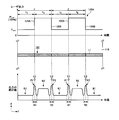
- FIG. 2 shows an example of the stress distribution form in the complex refraction region obtained when the output-modulated laser beam is scanned on the glass substrate, corresponding to the output waveform of the laser beam and the laser beam scanning position of the glass substrate.
- the laser light output waveform 125A is composed of a repetitive waveform of period ⁇ , and the vertical axis laser output is stepped with respect to the time on the horizontal axis. Repeat increasing and decreasing.
- the one period tau composed of the period t 1 the output is the minimum value P min, and the period t 2 which output is maximized P max.
- the minimum value P min is a value larger than 0 (zero), and is a value at which the temperature of the irradiated portion is equal to or higher than the strain point of the glass.
- the laser output on the vertical axis is normalized so that the maximum value P max is 100%.
- the relationship between the maximum value P max and the minimum value P min is not particularly limited.
- the minimum value P min may be in the range of 50% to 75% of the maximum value P max .
- the minimum value P min period t 1 and time t 2 of the maximum value P max of is are equal, the minimum value P min and duration of the maximum value P max, although different good.
- a birefringent region pattern 150 is formed on the glass substrate 110 along the scanning direction (Y direction) as shown in the middle of FIG.
- the laser beam is always scanned with an output equal to or higher than the minimum value P min , and this value is a value other than zero and the temperature of the irradiated portion is equal to or higher than the strain point of the glass.
- P min the minimum value
- P min the temperature of the irradiated portion is equal to or higher than the strain point of the glass.
- a non-birefringent region is not formed, and a linear pattern 150 including only a birefringent region is formed at the scanning position.
- the absolute value of stress at each position along the broken line L1 of the pattern 150 shows a stress distribution as shown at the bottom of FIG. That is, the stress distribution is a stress distribution in which a flat portion B1 of the first tensile stress, a peak portion P1 of the first compressive stress, a flat portion B2 of the second tensile stress, and a peak portion P2 of the second compressive stress are repeated. Arise.
- Such a stress distribution is obtained from the retardation distribution obtained from the birefringence measurement by a polarizing microscope, the fast axis direction distribution, the photoelastic constant of the glass, and the birefringence region thickness.
- the first compressive stress peak P1 is generated corresponding to the portion 126A where the output rapidly increases from P min to P max in the output waveform 125A of the laser beam
- the second compressive stress peak P2 is the laser beam.
- the output waveform 125A the output is generated corresponding to the portion 126B where the output drops rapidly from Pmax to Pmin .
- the flat portion B1 of the first tensile stress is generated in the region of the glass substrate 110 corresponding to the time when the output is P min .
- the flat portion B2 of the second tensile stress is generated in the region of the glass substrate 110 corresponding to the time between the peaks P1 and P2 and when the output becomes Pmax .
- the flat portion B2 of the second tensile stress has a larger stress value than the flat portion B1 of the first tensile stress.
- the first compressive stress peak P1 of the pattern 150 in the birefringent region is strictly more time than the rapidly increasing portion 126A of the output waveform 125A of the laser beam.
- the second compression stress peak P2 in the stress distribution is strictly delayed from the sudden drop portion 126B of the laser light output waveform 125A. (In the right side of FIG. 2). The same applies to the flat portions B1 and B2 of tensile stress.
- the birefringent region pattern 150 obtained when the output-modulated laser beam is used exhibits a stress distribution as shown in FIG.
- the glass substrate 110 is cut at a portion where the compressive stress in the pattern 150 of the birefringence region remains, and at the time of cutting. It is possible to significantly suppress the occurrence of cracks and cracks at the cut portion.
- the vicinity of the first compressive stress peak P1 (any position in the region R1) is selected as the first cutting part C1
- the second cutting part C2 is the second cutting part C2.
- the first cutting part C1 a position within the region R1 and earlier in time than the top position of the compressive stress peak P1 (left side in FIG. 2) is selected, and as the second cutting part C2, the position within R2
- the region R1 includes a flat portion B1 of the tensile stress formed “first” in time in the pattern 150 of the birefringent region, and a tensile force formed “after” in time closest to the flat portion B1.
- the region R2 is defined as a region between the stress flat portions B2, and the region R2 is a time period closest to the tensile stress flat portion B2 formed in the birefringent region pattern 150 in “time” in advance. In particular, it is defined as a region between the flat portions B1 of the tensile stress formed “after”.
- the production method according to the present invention can provide a retardation plate having a significantly high strength on the cut surface.
- the manufacturing method of the present invention unlike the method of cutting the glass substrate at the portion of the non-birefringent region that is not affected by the heat of the laser beam, it is avoided that the product size of the retardation plate is increased. Therefore, it is possible to reduce the size of the retardation plate.
- the reason why the stress distribution of the pattern 150 in the birefringent region shows such an aspect is not necessarily clear.
- the stress distribution is closely related to the amount of heat input of the laser beam, and tensile stress occurs in the region where the amount of heat input per unit time of the laser beam is almost constant, and the amount of heat input per unit time of the laser beam. Since there is a tendency for compressive stress to occur in a region where the temperature changes rapidly, it is presumed that a stress distribution as shown in FIG. 2 is obtained as a result of such a tendency.
- the output waveform 125A of the laser beam shown in FIG. 2 is merely an example, and in the present invention, a modulated laser beam having another output waveform may be used.
- FIG. 3 shows the stress distribution form of the birefringence region obtained when using a laser beam having an output waveform 125B different from the output waveform 125A shown in FIG. 2, and shows the output waveform of the laser beam and the laser beam of the glass substrate. This is schematically shown in correspondence with the scanning position.
- the laser beam has an output waveform 125B that repeats on / off, and the laser output on the vertical axis increases or decreases stepwise with respect to the time on the horizontal axis. . Is one period ⁇ of the output waveform 125B, composed of the period t 1 the output becomes 0, and the period t 2 the output is 100%. Note that the laser output on the vertical axis is standardized so that the maximum output value is 100%.
- the output waveform 125B of FIG. 3 the time period t 1 the output becomes 0, the output is the period t 2 to be 100%, but are equal, both period may be different.
- a birefringence region 145 and non-birefringence are formed on the glass substrate 110 along the scanning direction (Y direction) as shown in the middle stage of FIG.
- a repeated pattern 150 of the region 147 is formed.
- the stress absolute value at each position along the broken line L1 of the repetitive pattern 150 shows a stress distribution as shown at the bottom of FIG. That is, in one birefringent region 145, the first and second compressive stress peaks P1 and P2 and a flat portion B2 of tensile stress appear.
- the first compressive stress peak P1 is generated corresponding to the portion 126A where the output sharply increases in the output waveform 125B of the laser beam
- the second compressive stress peak P2 is generated in the output waveform 125B of the laser beam. It occurs corresponding to the portion 126B where the output drops rapidly.
- the compressive stress peak P1 occurs in the vicinity of the front end portion 148 of the birefringent region 145 when viewed along the scanning direction of the laser beam
- the compressive stress peak P2 is generated after the birefringent region 145. It occurs in the vicinity of the end 149.
- a flat portion B2 of tensile stress is generated between the peaks P1 and P2.
- the flat portion B ⁇ b> 2 of tensile stress is generated at a substantially central portion of the birefringent region 145.
- the first compressive stress peak P1 of the pattern 150 in the birefringent region is strictly more time than the rapidly rising portion 126A of the output waveform 125B of the laser beam.
- the second compression stress peak P2 in the stress distribution is also delayed in time from the steeply descending portion 126B of the output waveform 125B of the laser beam. (In the right side of FIG. 3). The same applies to the flat portion B2 of tensile stress.
- the front end portion 148 of the birefringent region 145 of the pattern 150 of the birefringent region is strictly more than the sharply rising portion 126A of the output waveform 125B of the laser beam.
- the rear end portion 149 of the birefringent region 145 of the pattern 150 of the birefringent region is at a time later than the steeply descending portion 126B of the output waveform 125B of the laser beam. Exists at a later position (on the right side of FIG. 3).
- the glass substrate 110 is cut at a portion where the compressive stress in the pattern 150 of the birefringence region remains. . That is, the vicinity of the first compressive stress peak P1 (any position in the region R3) is selected as the first cut portion C1, and the vicinity of the second compressive stress peak P2 is selected as the second cut portion C2. (Any position in the region R4) is selected. Thereby, it can suppress significantly that a crack and a crack arise in a cut part in the case of cutting.
- the region R3 is a region of the birefringent region pattern 150 in which the residual stress that exists “first” in time is zero and the tensile stress that is closest to this and formed “after” in time.
- the region R4 is defined as a region between the flat portions B2, and the region R4 is formed in the pattern 150 of the birefringent region, with the flat portion B2 of the tensile stress formed “temporarily” in time, and the temporally closest to this. It is defined as the region between the regions where the residual stress existing “after” is zero.
- the output period t 1 is shorter becomes 0, the pattern 150 of birefringent regions, non-birefringent region 147 (i.e., the residual stress becomes zero area ) May not be formed.
- the regions R3 and R4 may be determined based on the determination method of the regions R1 and R2 shown in FIG.
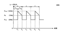
- the output waveform 125C of the laser beam, one cycle ⁇ is a constant minimum value P min in the time period (t 1) until time 0 ⁇ T 1, the period up to the time T 1 ⁇ T 2 (t 2 ) laser output in is composed of a waveform decreases monotonically from a maximum value P max to P a. (After that, at time T 2, the output returns to P min.)
- the minimum value P min is assumed to be 50% of the output of the maximum value P max .
- P A is has a 75% of P max, P A may be any value between P max of P min.
- P A P max
- the periods t 1 and t 2 are equal, but the periods t 1 and t 2 may be different.
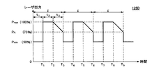
- FIG. 5 shows still another example of an output waveform of laser light that can be used in the present invention.
- this output waveform 125D one period ⁇ has a fixed minimum value P min in a period (t 1 ) from time 0 to T 1 and a fixed maximum value P max in a period (t 2 ) from time T 1 to T 2.
- P min a fixed minimum value
- P max a fixed maximum value
- the minimum value P min is assumed to be 50% of the output of the maximum value P max .
- P A is has a 75% of P max
- P A may be any value between P max of P min.
- P A P max
- the periods t 1 , t 2 , and t 3 are equal, but the periods t 1 , t 2 , and t 3 are not limited to this.
- the periods t 1 , t 2 , and t 3 may be different.
- FIG. 6 shows still another example of an output waveform that can be used in the present invention.
- 1 cycle ⁇ is the time 0 to the predetermined minimum value P min in the time period (t 1) to T 1, time T 1 ⁇ T period until 2 (t 2) the laser output at the P A a portion monotonously increases to P max from the duration of the portion where the laser output is constant maximum value P max in the time period (t 3) up to the time T 2 ⁇ T 3, until time T 3 ⁇ T 4 (t 4 ) Is constituted by a waveform that monotonously decreases from the maximum value P max to P B.
- the minimum value P min is assumed to be 50% of the output of the maximum value P max .
- P A is has a 80% P max
- P A may be any value between P max of P min.
- P B is 60% of P max , but P B may be any value between P max and P min .
- the output waveform 125E is equal to the output waveform 125A of FIG.
- P A P max
- the periods t 1 , t 2 , t 3 and t 4 are all equal, but the periods t 1 , t 2 , t 3 and t 4 are not limited to this.
- the periods t 1 , t 2 , t 3 and t 4 may be different.
- output waveforms can be considered.
- another repetitive waveform may be formed by combining at least two or more of the output waveforms 125A to 125E shown in FIGS.
- the output waveform of the laser beam is between the minimum value P min and a maximum value P max period (e.g., period t 2 in FIG. 4, a period t 3 in FIG. 5, and the period t 4 in FIG. 6) when the provided improves the uniformity of retardation distribution birefringent region.
- a maximum value P max period e.g., period t 2 in FIG. 4, a period t 3 in FIG. 5, and the period t 4 in FIG. 6
- the uniformity of the retardation distribution in the birefringent region is further improved. This is because a local temperature increase of the glass substrate is suppressed to some extent during the scanning of the laser light, and a region where the temperature is constant is likely to occur.
- the variation in the retardation distribution along the scanning direction in the birefringence region should be within ⁇ 5%. Can do.
- the variation of the retardation distribution in the direction perpendicular to the scanning direction in the birefringence region can be within ⁇ 5%.
- a retardation plate having a uniform retardation distribution in the birefringent region can be used as an element for a high-performance optical pickup device.
- FIG. 7 shows a schematic flow chart of an example of a method for producing a retardation film according to the present invention.
- FIG. 8 shows an example of an apparatus used in the method of manufacturing a retardation plate according to the present invention.
- the method of manufacturing a retardation plate according to the present invention includes (A) preparing a glass substrate having first and second surfaces (step S110); (B) scanning the output-modulated laser beam in the glass substrate and / or on the glass substrate in a first direction parallel to the first or second surface; Forming a birefringent region having a tensile stress portion and a compressive stress portion along the direction of 1 (step S120); (C) cutting the glass substrate so as to pass through the compressive stress portion of the birefringent region (step S130);
- FIG. 8 shows an example of an apparatus used in the method of manufacturing a retardation plate according to the present invention.
- an apparatus 200 used in the method of manufacturing a retardation film according to the present invention includes a laser beam 220 emitted from a laser light source (not shown) and a plurality of branched laser beams.
- a diffractive optical element 250 that branches into light 260A, 260B, and 260C and a lens 230 that converges each branched laser beam 260A, 260B, and 260C to a desired position on the glass substrate 210 are provided.
- the laser light source is not particularly limited, but an excimer laser light source (XeCl: wavelength 308 nm, KrF: wavelength 248 nm, ArF: wavelength 193 nm), YAG laser light source (wavelength 1064 nm), YVO4 laser light source (wavelength 1064 nm), titanium sapphire laser light source (Wavelength 800 nm) or a carbon dioxide laser light source (wavelength 10.6 ⁇ m) may be used.
- the YAG laser light source and the YVO4 laser light source may be, for example, a second harmonic wave source or a third harmonic wave laser source in addition to the fundamental wave described above.
- a second harmonic YAG laser has a wavelength of 532 nm
- a third harmonic YAG laser has a wavelength of 355 nm.
- the power of the laser light source is not particularly limited, but the larger the power of the laser light source, the more branched laser light can be obtained at one time, which is advantageous in expanding the birefringence region width.
- the diffractive optical element 250 may be any element as long as it can divide one laser beam 220 into a plurality of branched laser beams 260A, 260B, and 260C.
- the diffractive optical element 250 may be a beam instead of a diffractive optical element.
- a splitter or the like may be used.
- Step S110 First, a glass substrate 210 for constituting a phase difference plate is prepared.
- the glass substrate 210 has first and second surfaces.
- the composition of the glass substrate 210 is not particularly limited.
- the glass substrate 210 may be, for example, soda lime glass, borosilicate glass, and silica glass.
- glass doped with a transition metal or the like may be used as the glass substrate 210 in order to increase the absorption coefficient at the wavelength of the laser light 220 to be used.
- the thickness of the glass substrate is not particularly limited.
- the thickness of the glass substrate may be in the range of 0.1 mm to 3 mm, for example.
- Step S120 laser light 220 is emitted from the laser light source toward the glass substrate 210.
- the laser light 220 is branched into, for example, three or more branched beams 260 (260A, 260B, 260C).
- the branched beams 260A, 260B, and 260C are converged by the lens 230, and the focal points 270A, 270B, and 270C are formed inside or on the surface of the glass substrate 210, respectively.
- the focal points 270A, 270B, 270C are arranged in a straight line.
- the spot diameters of the focal points 270A, 270B, and 270C vary depending on the performance of the lens 230 and the like, but may be, for example, about 0.1 ⁇ m to 100 ⁇ m.
- the distance between the focal points 270A, 270B, and 270C is not particularly limited, but due to restrictions on the apparatus configuration, the realistic distance is in the range of 20 ⁇ m to 400 ⁇ m, and preferably in the range of 50 ⁇ m to 250 ⁇ m.
- the series of branched beams 260A, 260B, and 260C are scanned in the first direction (Y direction in the example of FIG. 2).
- the scanning speed of each of the branched beams 260A, 260B, and 260C varies depending on the distance between the focal points 270A, 270B, and 270C, but ranges from 0.1 mm / second to 50 mm / second, for example.
- tensile stress parallel to the scanning direction is generated in the region where the branched beams 260A, 260B, and 260C are scanned, thereby forming rod-shaped birefringence region patterns 290A, 290B, and 290C.
- the branched beams are also heated by heat conduction, and on the glass substrate 210 or in the scanning direction.
- a uniaxial birefringent region pattern 290 that is continuous in a direction perpendicular to the surface and has a relatively large area can be formed.
- the branched beams 260A, 260B, and 260C are output-modulated.
- the diffractive optical element 250 divides one laser beam 220 into three branched beams 260A, 260B, and 260C.
- one laser beam 220 may be divided into two or four or more branched beams by the diffractive optical element 250.
- the apparatus 200 may not have the diffractive optical element 250. In this case, one laser beam 220 is used as it is as a scanning laser beam without being branched.
- the number of branches used may be any number.
- the number of branches is appropriately selected in consideration of, for example, the necessary width of the birefringent region pattern 290 in the direction perpendicular to the scanning direction of the laser beam (X direction in FIG. 8) or the manufacturing time.
- a region having a diameter of at least 500 ⁇ m ⁇ is required as a birefringent region.
- a laser beam branched into six and having a focal interval of 100 ⁇ m may be used.
- step S120 may be repeated as many times as necessary.
- the width of the birefringent region pattern 290 formed at a time is 200 ⁇ m.
- a birefringent region having a width of 500 ⁇ m or more is formed by repeating the above scanning three times or more by shifting the scanning start point of the branched beams 260A, 260B, and 260C by 200 ⁇ m in the X direction each time scanning is performed. Can do.
- a retardation plate having a birefringence region pattern at least in a region having a diameter of 500 ⁇ m ⁇ can be finally manufactured.
- the variation in the retardation distribution along the scanning direction in the birefringence region. Can be within ⁇ 5%.
- the retardation distribution in the direction perpendicular to the scanning direction can be suppressed relatively easily by controlling the distance between the focal points of the branched beams. Therefore, in the present invention, a retardation plate having a uniform retardation distribution can be produced along the stretching direction and the vertical direction of the birefringent region.
- Step S130 the glass substrate 210 is cut (diced) to manufacture a retardation plate. As described above, at this time, the glass substrate 210 is cut so as to pass through the portion where the compressive stress remains in the birefringence region pattern, and thus, at the time of cutting, a crack or a crack occurs in the cut portion. This can be significantly suppressed.
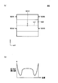
- FIG. 9A shows a schematic top view of the retardation film 900 manufactured by the method according to the present invention.
- FIG. 9B shows a schematic stress distribution in the region along the broken line L2 of the retardation film 900.
- FIG. 9A shows a schematic top view of the retardation film 900 manufactured by the method according to the present invention.
- FIG. 9B shows a schematic stress distribution in the region along the broken line L2 of the retardation film 900.
- the retardation film 900 is a birefringent region that continuously extends from one end surface 925A to the other end surface 925B of the glass substrate 910 along one direction (Y direction). 930.
- a laser beam whose output is modulated is used as the laser beam for forming the birefringent region 930.
- the birefringent region pattern is cut so as to cross the compressive stress portion.
- a retardation film 900 having a relatively high strength can be obtained.
- the birefringent region 930 can have a relatively uniform retardation distribution.
- a region of ⁇ 250 ⁇ m that is, a total of 500 ⁇ m
- the variation in retardation distribution can be suppressed to within ⁇ 5%.
- the variation in retardation distribution is suppressed to within ⁇ 5%. can do.
- Such a retardation plate 900 can be used as a quarter-wave plate or a half-wave plate of an optical pickup device.
- the retardation plate manufactured by the above-described method can be used as a quarter-wave plate and / or a half-wave plate for an optical pickup device.
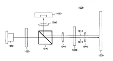
- FIG. 10 shows a schematic diagram of such an optical pickup device.
- an optical pickup apparatus 1000 includes a laser light source 1010 such as a blue LD (wavelength 405 nm), a half-wave plate 1020, a polarization beam splitter 1030, a quarter-wave plate 1050, and a Blu-ray disc.
- a laser light source 1010 such as a blue LD (wavelength 405 nm)
- a half-wave plate 1020 such as a polarization beam splitter 1030, a quarter-wave plate 1050, and a Blu-ray disc.
- Such an optical recording medium 1070 and a photodiode 1090 are provided.
- the optical recording medium 1070 may be an optical recording medium such as a CD or a DVD.
- the laser light source 1010 may be a light source having a wavelength of 780 nm (in the case of CD) or a wavelength of 650 nm (in the case of DVD).
- the half-wave plate 1020 is a member for giving an optical path difference of ⁇ / 2 (, that is, a phase difference of ⁇ ) between two orthogonal polarization components having a specific wavelength (for example, 405 nm in the case of blue laser light). is there.
- the quarter-wave plate 1050 is for giving an optical path difference of ⁇ / 4 (, that is, a phase difference of ⁇ / 2) between two orthogonal polarization components having a specific wavelength (for example, 405 nm in the case of blue laser light). It is a member.
- linearly polarized light (parallel to the paper surface) 1012 emitted from the laser light source 1010 passes through the half-wave plate 1020, where the polarization plane of the linearly polarized light is rotated.
- the light 1012 further passes through the polarizing beam splitter 1030 and the collimating lens 1040 and is guided toward the quarter-wave plate 1050.
- the light 1012 that has passed through the quarter-wave plate 1050 is polarized from linearly polarized light to circularly polarized light, and then irradiated onto the optical recording medium 1070 by the objective lens 1060.
- the light 1013 reflected from the optical recording medium 1070 is guided to the quarter-wave plate 1050 through the same optical path.
- the light 1013 is polarized into linearly polarized light (perpendicular to the paper surface), and then irradiated to the polarization beam splitter 1030 and guided to the photodiode 1090 through the lens 1080.
- Information on the optical recording medium 1070 is read by the photodiode 1090.
- the half-wave plate 1020 and / or the quarter-wave plate 1050 are formed of a retardation plate manufactured by the method according to the present invention. That is, in the half-wave plate 1020 and / or the quarter-wave plate 1050, the retardation distribution in the birefringence region is significantly suppressed. Therefore, in this optical pickup device 1000, the light emitted from the half-wave plate 1020 and / or the quarter-wave plate 1050 can be adjusted to a desired polarization state, and wavefront aberration can be suppressed.
- Example 1 Using the apparatus as shown in FIG. 8, a retardation plate was manufactured in the following procedure.
- a glass substrate (borosilicate glass) having a plate thickness of 1 mm was prepared.
- the scanning speed was 2 mm / second.
- Coherent AVIA-X having a wavelength of 355 nm was used.
- the laser beam was split into five laser beams by a diffractive optical element.
- Each laser beam was condensed in a glass substrate by a lens (theoretical spot diameter: 0.5 ⁇ m).
- the focal points of the laser beams were linearly arranged in the glass substrate, and the distance between the focal points in the glass substrate was 150 ⁇ m.
- the output waveform of each laser beam was in the form shown in FIG.
- the minimum output value P min of the laser beam was zero, and the period t 1 was 1 sec.
- the maximum output value P max of the laser beam was 14 W, and the period t 2 was 1 sec.
- the output value P A is set to 10.5 W, the period t 3 was set to 1 sec.
- the laser beam was scanned only once.
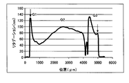
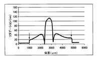
- FIG. 11 shows a part of the measurement result of the retardation distribution of the birefringence region pattern (for one period) in the scanning direction of the laser beam.
- FIG. 12 shows an example of the measurement result of the retardation distribution of the birefringent region pattern in a direction perpendicular to the laser beam scanning direction (hereinafter referred to as “(laser beam) width direction”). .
- a birefringence imaging system Abrio manufactured by Cri was used for the measurement of this retardation.
- a configuration is used in which a light source and a circular polarization filter are arranged in front of a sample, and an ellipsometer and a CCD camera are arranged behind the sample.
- the state of the liquid crystal optical element in the ellipsometer is changed, a plurality of images that have passed through the ellipsometer are acquired by a CCD camera, and these images are compared and calculated. Can be quantified.
- the birefringent region pattern includes a first retardation peak Q1 (position of about 800 ⁇ m), a flat portion Q2 of retardation (position of about 2000 ⁇ m to about 4500 ⁇ m), and a second retardation peak.
- Q1 position of about 800 ⁇ m
- Q2 flat portion of retardation
- Q3 about 5000 ⁇ m position
- the birefringent region pattern includes a first retardation peak Q4 (position of about 1700 ⁇ m) and a flat portion Q5 of retardation (about 2100 ⁇ m to about 2900 ⁇ m). ) And the second retardation peak Q6 (position of about 3200 ⁇ m) is observed.
- the glass substrate was cut along the scanning direction and the width direction of the laser beam.
- the cutting position of the glass substrate in the scanning direction was set at the positions indicated by arrows S1 and S2 in FIG.
- disconnection location of the glass substrate in the width direction was made into the position shown by arrow S3 and S4 in FIG.
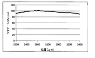
- FIG. 13 shows the measurement result of the retardation distribution in the birefringence region in the scanning direction of the obtained retardation plate.
- FIG. 14 shows the measurement results of the retardation distribution in the birefringence region in the width direction of the obtained retardation plate.
- the position of the arrow indicates the end face of the retardation film.
- the birefringent region is cut at the position of the first retardation peak Q1 and the second retardation peak Q3 in the scanning direction, and compressive stress is generated on the end face of the retardation plate.
- FIG. 14 shows that the birefringent region is cut at the compressive stress portion also in the width direction, and compressive stress is generated on the end face of the retardation plate.
- FIG. 15 shows an enlarged view of the flat portion Q2 in FIG.
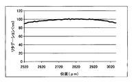
- FIG. 16 shows an enlarged view of the flat portion Q5 in FIG.
- FIG. 15 shows that the retardation plate has a retardation distribution variation within ⁇ 5% over a wide region of 500 ⁇ m in the scanning direction.
- FIG. 16 shows that in the retardation plate, the variation in retardation distribution is suppressed within ⁇ 5% over a wide region of 500 ⁇ m in the width direction.
- the retardation plate obtained by the method according to the present invention can obtain a relatively uniform retardation distribution in the birefringent region over a wide range of 500 ⁇ m in length and width.
- Example 2 A retardation plate was produced in the same manner as in Example 1.
- the minimum output value P min of the laser beam was set to 7W.
- the cut surface of the retardation plate was in a healthy state with no cracks or cracks observed.
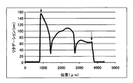
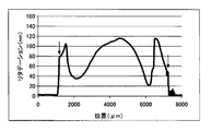
- FIG. 17 shows the measurement result of the retardation distribution of the birefringent region in the laser beam scanning direction after cutting the glass substrate. Moreover, in FIG. 18, the measurement result of the retardation distribution of the birefringent area
- Example 3 A retardation plate was produced in the same manner as in Example 1.
- Example 3 the laser output waveform of each laser beam was in the form shown in FIG.
- the maximum output value P max of the laser beam was 14 W, and the times t 1 and t 2 were both 2 sec.
- the cut surface of the retardation plate was in a healthy state with no cracks or cracks observed.
- FIG. 19 shows the measurement result of the retardation distribution of the birefringence region in the laser beam scanning direction after cutting the glass substrate.
- FIG. 20 shows the measurement result of the retardation distribution of the birefringent region in the width direction of the laser light after cutting the glass substrate.
- the position of the arrow indicates the end face of the phase difference plate.
- Example 4 A retardation plate was produced in the same manner as in Example 1.
- Example 4 the laser output waveform of each laser beam was in the form shown in FIG.
- the maximum output value P max of the laser beam was 14 W
- the minimum output value P min of the laser beam was 7 W
- the times t 1 and t 2 were both 2 sec.
- the cut surface of the retardation plate was in a healthy state with no cracks or cracks observed.
- FIG. 21 shows the measurement result of the retardation distribution of the birefringent region in the laser beam scanning direction after cutting the glass substrate.
- FIG. 22 shows the measurement result of the retardation distribution of the birefringent region in the width direction of the laser light after cutting the glass substrate. 21 and 22, the position of the arrow indicates the end face of the retardation plate.
- the retardation plate produced by the method according to the present invention has a compressive stress remaining in the birefringent region, has high strength, and has a relatively uniform retardation distribution.
- the present invention can be applied to optical components such as a phase difference plate, a half-wave plate, a quarter-wave plate, an optical pickup element, and an isolator.
Landscapes
- Physics & Mathematics (AREA)
- Optics & Photonics (AREA)
- Engineering & Computer Science (AREA)
- Chemical Kinetics & Catalysis (AREA)
- General Chemical & Material Sciences (AREA)
- Oil, Petroleum & Natural Gas (AREA)
- Chemical & Material Sciences (AREA)
- Plasma & Fusion (AREA)
- Mechanical Engineering (AREA)
- General Physics & Mathematics (AREA)
- Polarising Elements (AREA)
- Laser Beam Processing (AREA)
- Optical Head (AREA)
Abstract
ガラス基板をダイシングやスクライブ割断してチップ化された位相差板を得る際に、切断部分に割れやクラックが発生し難い位相差板の製造方法を提供することを目的とする。 ガラス基板内および/またはガラス基板上に複屈折領域を有する位相差板の製造方法であって、(a)第1および第2の表面を有するガラス基板を準備し、(b)前記ガラス基板内および/またはガラス基板上に、出力変調されたレーザ光を、前記第1または第2の表面と平行な第1の方向に走査して、前記ガラス基板に、前記第1の方向に沿って、引張応力部分および圧縮応力部分を有する複屈折領域を形成し、(c)前記ガラス基板を、前記複屈折領域の圧縮応力部分を通るように切断することを特徴とする位相差板の製造方法。
Description
本発明は、位相差板の製造方法および位相差板に関する。
光の位相や偏光を制御することが可能な位相差板(例えば、1/2波長板または1/4波長板など)は、ブルーレイ光ピックアップ装置を含む、様々な光学機器等に使用されている。
これまでこのような位相差板には、屈折率異方性、すなわち複屈折を有する有機高分子フィルムや一軸性結晶である水晶等が使用されてきた。
しかしながら、有機高分子フィルムは、耐湿性や高温安定性に劣る。また、水晶は材料自体が高価な上、正確な厚みへの切り出しや研磨等の加工コストが高い。そのため、耐湿性および高温安定性、低コスト性に優れるガラス基板を用いて、位相差板を製造する方法が提案されている。例えば、特許文献1には、レーザ光を使用して、ガラス基板内に、帯状の複屈折領域を形成する方法が開示されている。
前述の特許文献1の方法では、レーザ光をガラス基板に照射し、これを走査することにより、ガラス基板内に、帯状の複屈折領域を形成することができる。
しかしながら、このような複屈折領域を有するガラス基板を、実際に位相差板の製品として提供するためには、帯状の複屈折領域を横断するようにガラス基板を切断(ダイシングやスクライブ割断)して、ガラス基板をチップ化する必要がある。
ここで、前述の特許文献1の方法で得られたガラス基板の場合、帯状の複屈折領域は、レーザ光照射の熱影響による引張応力により発生したものであるため、そのようなガラス基板の帯状複屈折領域を横断するようにしてガラス基板を切断した場合、切断部分にクラックが発生したり、ガラス基板が割れてしまう可能性がある。
本発明は、ガラス基板をダイシングやスクライブ割断してチップ化された位相差板を得る際に、切断部分に割れやクラックが発生し難い位相差板の製造方法を提供することを目的とする。また、切断部分の強度が向上された位相差板を提供することを目的とする。
本発明では、
ガラス基板内および/またはガラス基板上に複屈折領域を有する位相差板の製造方法であって、
(a)第1および第2の表面を有するガラス基板を準備し、
(b)前記ガラス基板内および/またはガラス基板上に、出力変調されたレーザ光を、前記第1または第2の表面と平行な第1の方向に走査して、前記ガラス基板に、前記第1の方向に沿って、引張応力部分および圧縮応力部分を有する複屈折領域を形成し、
(c)前記ガラス基板を、前記複屈折領域の圧縮応力部分を通るように切断することを特徴とする位相差板の製造方法が提供される。
ガラス基板内および/またはガラス基板上に複屈折領域を有する位相差板の製造方法であって、
(a)第1および第2の表面を有するガラス基板を準備し、
(b)前記ガラス基板内および/またはガラス基板上に、出力変調されたレーザ光を、前記第1または第2の表面と平行な第1の方向に走査して、前記ガラス基板に、前記第1の方向に沿って、引張応力部分および圧縮応力部分を有する複屈折領域を形成し、
(c)前記ガラス基板を、前記複屈折領域の圧縮応力部分を通るように切断することを特徴とする位相差板の製造方法が提供される。
ここで、本発明による製造方法において、
前記(b)において、前記複屈折領域の圧縮応力部分は、前記第1の方向に沿って、第1の圧縮応力部分および第2の圧縮応力部分を有し、前記複屈折領域の引張応力部分は前記第1及び2の圧縮応力部分の間の引張応力部分を有し、
前記(c)において、前記ガラス基板は、第1の切断位置および第2の切断位置で切断され、前記第1の切断位置として、前記第1の圧縮応力部分が選定され、第2の切断位置として、前記第2の圧縮応力部分が選定されても良い。
前記(b)において、前記複屈折領域の圧縮応力部分は、前記第1の方向に沿って、第1の圧縮応力部分および第2の圧縮応力部分を有し、前記複屈折領域の引張応力部分は前記第1及び2の圧縮応力部分の間の引張応力部分を有し、
前記(c)において、前記ガラス基板は、第1の切断位置および第2の切断位置で切断され、前記第1の切断位置として、前記第1の圧縮応力部分が選定され、第2の切断位置として、前記第2の圧縮応力部分が選定されても良い。
また、本発明による製造方法において、
前記出力変調されたレーザ光は、時間に対して、レーザ出力がステップ状に増加する部分、および/またはレーザ出力がステップ状に減少する部分を有し、
前記第1の圧縮応力部分は、前記レーザ出力がステップ状に増加するレーザ光を照射することにより発生し、および/または
前記第2の圧縮応力部分は、前記レーザ出力がステップ状に減少するレーザ光を照射することにより発生しても良い。
前記出力変調されたレーザ光は、時間に対して、レーザ出力がステップ状に増加する部分、および/またはレーザ出力がステップ状に減少する部分を有し、
前記第1の圧縮応力部分は、前記レーザ出力がステップ状に増加するレーザ光を照射することにより発生し、および/または
前記第2の圧縮応力部分は、前記レーザ出力がステップ状に減少するレーザ光を照射することにより発生しても良い。
また、本発明による製造方法において、
前記出力変調されたレーザ光は、周期τの繰り返し波形を有しても良い。
前記出力変調されたレーザ光は、周期τの繰り返し波形を有しても良い。
また、本発明による製造方法において、
前記出力変調されたレーザ光は、レーザ出力の最小値および最大値を含み、
前記出力変調されたレーザ光の1周期τは、前記最小値の時間に対する平坦部、および/または前記最大値の時間に対する平坦部を有しても良い。
前記出力変調されたレーザ光は、レーザ出力の最小値および最大値を含み、
前記出力変調されたレーザ光の1周期τは、前記最小値の時間に対する平坦部、および/または前記最大値の時間に対する平坦部を有しても良い。
また、本発明による製造方法において、前記最小値は、0以外の値であっても良い。
また、本発明による製造方法において、前記レーザ光は、各焦点が一列に配列された2本以上のレーザ光で構成されても良い。
さらに、本発明では、
ガラス基板内および/またはガラス基板上に複屈折領域を有する位相差板であって、
前記複屈折領域は、第1の方向に沿って、前記ガラス基板の第1の端面から第2の端面まで延伸されており、
前記複屈折領域は、前記第1の方向に沿った500μmの長さの領域でのリタデーション分布の変動が±5%以内であることを特徴とする位相差板が提供される。
ガラス基板内および/またはガラス基板上に複屈折領域を有する位相差板であって、
前記複屈折領域は、第1の方向に沿って、前記ガラス基板の第1の端面から第2の端面まで延伸されており、
前記複屈折領域は、前記第1の方向に沿った500μmの長さの領域でのリタデーション分布の変動が±5%以内であることを特徴とする位相差板が提供される。
ここで、本発明による位相差板において、前記複屈折領域は、前記第1の方向に垂直な第2の方向に沿った500μmの長さの領域でのリタデーション分布の変動が±5%以内であっても良い。
本発明では、ガラス基板をダイシングやスクライブ割断してチップ化された位相差板を得る際に、切断部分に割れやクラックが発生し難い位相差板の製造方法を提供することができる。また、切断部分の強度が向上された位相差板を提供できる。
以下、本発明について説明する。
まず、本発明の特徴をより良く理解するため、特許文献1に記載された従来技術の位相差板の製造方法について、簡単に説明する。
図1には、特許文献1に記載された位相差板の製造方法の概念図を示す。
図1に示すように、この方法では、レンズ3を介して、ガラス基板1にレーザ光2が照射される。レーザ光2を図1のY方向に沿って走査させることにより、ガラス基板1内に、帯状の複屈折領域4を形成することができる。
このような複屈折領域4を有するガラス基板1を、実際に位相差板製品として提供するためには、帯状の複屈折領域4を横断するように(例えば図1のX方向に沿って)ガラス基板1を切断(ダイシングやスクライブ割断)して、ガラス基板1をチップ化する必要がある。
しかしながら、ガラス基板1において、帯状の複屈折領域4は、レーザ光2の照射の熱影響による引張応力により発生したものであるため、ガラス基板1の帯状複屈折領域を横断するようにしてガラス基板1を切断した場合、切断部分にクラックが発生したり、ガラス基板1が割れてしまう可能性がある。
このようなクラックや割れを防ぐため、予めガラス基板に照射するレーザ光の出力をオン/オフ変調させておくことが考えられる。この場合、複屈折領域は、レーザ光の走査方向(Y方向)に沿って、断続的に形成されるようになる。また、複屈折領域同士の間には、非複屈折領域が形成される。従って、位相差板の製品を切り出す際には、非複屈折領域を通るようにして、ガラス基板をダイシングやスクライブ割断することにより、前述のようなクラックや割れが軽減されると考えられる。
ただし、このような方法では、レーザ光の出力がオフとなる時間を十分に長くして、複屈折領域同士の間に、比較的長いレーザ光未照射領域を形成する必要がある。これは、レーザ光の出力がオンからオフに切り替わった後も、ある期間までは、ガラス基板の温度が上昇し続けるためである。逆に、レーザ光の出力がオフとなる時間が不十分な場合、レーザ光未照射領域においても、熱影響部分が発生してしまい、非熱影響部分を十分に確保することができなくなる。
製品となる位相差板は、レーザ光未照射領域の非熱影響部分(すなわち非複屈折領域)同士の間で切断して製造する必要がある。従って、このような方法では、製品の寸法が大きくなってしまい、製品の小型化が難しくなってしまう。
本願発明者らは、レーザ光の出力波形とこれによって生じる複屈折領域の形態との間の関係について、様々な検討を行ってきた。その結果、出力が変調されたレーザ光を使用した場合、形成される複屈折領域には、レーザ光の走査方向に沿って、引張応力部分と圧縮応力部分とが存在することを見出し、本発明に至った。
すなわち、本発明では、
ガラス基板内および/またはガラス基板上に複屈折領域を有する位相差板の製造方法であって、
(a)第1および第2の表面を有するガラス基板を準備し、
(b)前記ガラス基板内および/またはガラス基板上に、出力変調されたレーザ光を、前記第1または第2の表面と平行な第1の方向に走査して、前記ガラス基板に、前記第1の方向に沿って、引張応力部分および圧縮応力部分を有する複屈折領域を形成し、
(c)前記ガラス基板を、前記複屈折領域の圧縮応力部分を通るように切断することを特徴とする位相差板の製造方法が提供される。
ガラス基板内および/またはガラス基板上に複屈折領域を有する位相差板の製造方法であって、
(a)第1および第2の表面を有するガラス基板を準備し、
(b)前記ガラス基板内および/またはガラス基板上に、出力変調されたレーザ光を、前記第1または第2の表面と平行な第1の方向に走査して、前記ガラス基板に、前記第1の方向に沿って、引張応力部分および圧縮応力部分を有する複屈折領域を形成し、
(c)前記ガラス基板を、前記複屈折領域の圧縮応力部分を通るように切断することを特徴とする位相差板の製造方法が提供される。
図2には、出力変調されたレーザ光を、ガラス基板上に走査した際に得られる複素屈折領域の応力分布形態の一例を、レーザ光の出力波形およびガラス基板のレーザ光走査位置と対応させて模式的に示す。
図2の例では、図の最上部に示すように、レーザ光の出力波形125Aは、周期τの繰り返し波形で構成され、縦軸のレーザ出力は、横軸の時間に対して、ステップ状の増減を繰り返す。この1周期τは、出力が最小値Pminとなる期間t1と、出力が最大値Pmaxとなる期間t2とで構成される。なお、最小値Pminは、0(ゼロ)よりも大きな値であり、かつ照射部の温度がガラスの歪点以上になる値である。また、縦軸のレーザ出力は、最大値Pmaxが100%となるように規格化して示している。
ここで、図2の出力波形125Aにおいて、最大値Pmaxと最小値Pminの関係は、特に限られない。例えば、最小値Pminは、最大値Pmaxの50%~75%の範囲であっても良い。
また、図2の例では、最小値Pminの期間t1と最大値Pmaxの期間t2は、等しくなっているが、最小値Pminと最大値Pmaxの期間は、異なっていても良い。
このような出力波形125Aを有するレーザ光を用いた場合、図2の中段に示すように、ガラス基板110上には、走査方向(Y方向)に沿って、複屈折領域のパターン150が形成される。
ここで、この例では、レーザ光は、常に最小値Pmin以上の出力で走査され、この値はゼロ以外の、照射部の温度がガラスの歪点以上になる値であるため、走査位置に非複屈折領域は形成されず、走査位置には、複屈折領域のみからなる直線状のパターン150が形成される。
また、このパターン150の破線L1に沿った各位置での応力絶対値は、図2の最下部に示すような応力分布を示すようになる。すなわち、応力分布として、第1の引張応力の平坦部分B1、第1の圧縮応力のピークP1、第2の引張応力の平坦部分B2、および第2の圧縮応力のピークP2を繰り返した応力分布が生じる。
なお、このような応力分布は、偏光顕微鏡による複屈折測定から得られるリタデーション分布、進相軸方向分布、ガラスの光弾性定数および複屈折領域厚さから得られる。
ここで、第1の圧縮応力ピークP1は、レーザ光の出力波形125Aにおいて、出力がPminからPmaxに急上昇する部分126Aに対応して発生し、第2の圧縮応力ピークP2は、レーザ光の出力波形125Aにおいて、出力がPmaxからPminに急降下する部分126Bに対応して発生する。一方、第1の引張応力の平坦部分B1は、出力がPminとなる時間に対応するガラス基板110の領域に生じる。また、第2の引張応力の平坦部分B2は、ピークP1とP2の間の、出力がPmaxとなる時間に対応するガラス基板110の領域に生じる。通常の場合、第2の引張応力の平坦部分B2は、第1の引張応力の平坦部分B1に比べて大きな応力値を有する。
なお、図2において、レーザ光の出力波形125A、複屈折領域のパターン150、および応力分布の相互の位置関係は、明確化のため、近似的に示されていることに留意する必要がある。
例えば、実際には、レーザ光の入熱の遅れがあるため、複屈折領域のパターン150の第1の圧縮応力ピークP1は、厳密には、レーザ光の出力波形125Aの急上昇部分126Aよりも時間的に遅れた位置に(図2のより右側に)形成され、応力分布における第2の圧縮応力のピークP2も、厳密には、レーザ光の出力波形125Aの急降下部分126Bよりも時間的に遅れた位置に(図2のより右側に)形成される。引張応力の平坦部分B1およびB2についても同様である。
出力変調されたレーザ光を使用した場合に得られる複屈折領域のパターン150は、ほとんどの場合、図2のような応力分布を示すことが、本願発明者らによって見出されている。
従って、ガラス基板110をダイシングやスクライブ割断して位相差板を製造する際には、複屈折領域のパターン150内の圧縮応力が残留する部分でガラス基板110を切断することにより、切断の際に、切断部分に割れやクラックが生じることを有意に抑制できる。
例えば、図2の例では、第1の切断部C1として、第1の圧縮応力ピークP1の近傍(領域R1内のいずれかの位置)を選定し、第2の切断部C2として、第2の圧縮応力ピークP2の近傍(領域R2内のいずれかの位置)を選定すれば良い。これにより、切断部分に割れやクラックが生じることを有意に抑制することができる。特に、第1の切断部C1として、領域R1内でかつ圧縮応力ピークP1の頂上位置よりも時間的に早い位置(図2の左側)を選定し、第2の切断部C2として、R2内でかつ圧縮応力ピークP2の頂点位置よりも時間的に遅れた位置(図2の右側)を選定することは、切断時の割れやクラック抑制の点から特に好ましい。
ここで、領域R1は、複屈折領域のパターン150において、時間的に「先に」形成された引張応力の平坦部分B1と、これに最近接の、時間的に「後から」形成された引張応力の平坦部分B2の間の領域として定められ、領域R2は、複屈折領域のパターン150において、時間的に「先に」形成された引張応力の平坦部分B2と、これに最近接の、時間的に「後から」形成された引張応力の平坦部分B1の間の領域として定められる。
さらに、製品の切断面には、圧縮応力が残留しているため、本発明による製造方法では、切断面が有意に高い強度を有する位相差板を提供することが可能となる。
また、本発明の製造方法の場合、ガラス基板を、レーザ光の熱影響を受けていない非複屈折領域の部分で切断する方法とは異なり、位相差板の製品寸法が大きくなることが回避されるため、位相差板を小型化することも可能になる。
ここで、複屈折領域のパターン150の応力分布がこのような態様を示す理由については、必ずしも明確ではない。ただし、応力分布は、レーザ光の入熱量と密接に関係しており、レーザ光の単位時間当たりの入熱量がほぼ一定の領域では、引張応力が発生し、レーザ光の単位時間当たりの入熱量が急激に変化する領域では、圧縮応力が発生する傾向にあることから、このような傾向の結果として、図2に示すような応力分布が得られるものと推定される。
以上、図2を参照して、本発明による位相差板の製造方法の概念を説明した。しかしながら、図2に示したレーザ光の出力波形125Aは、単なる一例に過ぎず、本発明において、その他の出力波形を有する変調レーザ光を使用しても良い。
図3には、図2に示した出力波形125Aとは異なる出力波形125Bを有するレーザ光を使用した際に得られる複屈折領域の応力分布形態を、レーザ光の出力波形およびガラス基板のレーザ光走査位置と対応させて模式的に示す。
図3の例では、図の最上部に示すように、レーザ光は、オン/オフを繰り返す出力波形125Bを有し、横軸の時間に対して、縦軸のレーザ出力がステップ状に増減する。出力波形125Bの1周期τは、出力が0になる期間t1と、出力が100%となる期間t2とで構成される。なお、縦軸のレーザ出力は、最大出力値が100%となるように規格化して示している。
ここで、図3の出力波形125Bでは、出力が0になる期間t1と、出力が100%となる期間t2とは、等しくなっているが、両者の期間は、異なっていても良い。
このような繰り返し波形125Bを有するレーザ光を用いた場合、図3の中段に示すように、ガラス基板110上には、走査方向(Y方向)に沿って、複屈折領域145と、非複屈折領域147の繰り返しパターン150が形成される。
また、繰り返しパターン150の破線L1に沿った各位置での応力絶対値は、図3の最下部に示すような応力分布を示すようになる。すなわち、一つの複屈折領域145内には、第1および第2の圧縮応力ピークP1およびP2と、引張応力の平坦部分B2とが現れる。
ここで、第1の圧縮応力ピークP1は、レーザ光の出力波形125Bにおいて、出力が急上昇する部分126Aに対応して発生し、第2の圧縮応力ピークP2は、レーザ光の出力波形125Bにおいて、出力が急降下する部分126Bに対応して発生する。別の言い方をすれば、圧縮応力ピークP1は、レーザ光の走査方向に沿って見たとき、複屈折領域145の前端部148の近傍に生じ、圧縮応力ピークP2は、複屈折領域145の後端部149の近傍に生じる。また、引張応力の平坦部分B2は、ピークP1とP2の間に生じる。換言すれば、引張応力の平坦部分B2は、複屈折領域145の略中央部分に生じる。
なお、図3においても、図2の場合と同様、レーザ光の出力波形125B、複屈折領域のパターン150、および応力分布の相互の位置関係は、明確化のため、近似的に示されていることに留意する必要がある。
例えば、実際には、レーザ光の入熱の遅れがあるため、複屈折領域のパターン150の第1の圧縮応力ピークP1は、厳密には、レーザ光の出力波形125Bの急上昇部分126Aよりも時間的に遅れた位置に(図3のより右側に)形成され、応力分布における第2の圧縮応力のピークP2も、厳密には、レーザ光の出力波形125Bの急降下部分126Bよりも時間的に遅れた位置に(図3のより右側に)形成される。引張応力の平坦部分B2についても同様である。
同様に、実際には、レーザ光の入熱の遅れがあるため、複屈折領域のパターン150の複屈折領域145の前端部148は、厳密には、レーザ光の出力波形125Bの急上昇部分126Aよりも時間的に遅れた位置に(図3のより右側に)存在し、複屈折領域のパターン150の複屈折領域145の後端部149は、レーザ光の出力波形125Bの急降下部分126Bよりも時間的に遅れた位置に(図3のより右側に)存在する。
この図3の例でも、ガラス基板110をダイシングやスクライブ割断して位相差板を製造する際には、ガラス基板110は、複屈折領域のパターン150内の圧縮応力が残留する部分で切断される。すなわち、第1の切断部C1として、第1の圧縮応力ピークP1の近傍(領域R3内のいずれかの位置)が選定され、第2の切断部C2として、第2の圧縮応力ピークP2の近傍(領域R4内のいずれかの位置)が選定される。これにより、切断の際に、切断部分に割れやクラックが生じることを有意に抑制することができる。
ここで、領域R3は、複屈折領域のパターン150において、時間的に「先に」存在する残留応力がゼロの領域と、これに最近接の、時間的に「後に」形成された引張応力の平坦部分B2の間の領域として定められ、領域R4は、複屈折領域のパターン150において、時間的に「先に」形成された引張応力の平坦部分B2と、これに最近接の、時間的に「後に」存在する残留応力がゼロとなる領域の間の領域として定められる。
なお、図3に示したレーザ光の出力波形125Bにおいて、出力が0になる期間t1が短くなると、複屈折領域のパターン150に、非複屈折領域147(すなわち、残留応力がゼロとなる領域)が形成されなくなる場合が生じ得る。このような場合、領域R3およびR4は、それぞれ、前述の図2に示した領域R1およびR2の判定方法に基づいて定めれば良い。
図4~図6には、本発明に使用され得るレーザ光の出力波形のさらに別の一例を示す。
図4では、レーザ光の出力波形125Cにおいて、1周期τは、時間0~T1までの期間(t1)における一定最小値Pminと、時間T1~T2までの期間(t2)におけるレーザ出力が最大値PmaxからPAまで単調減少する波形とで構成される。(その後、時間T2において、出力は、Pminに戻る。)
ここで、最小値Pminは、最大値Pmaxの50%の出力と仮定している。
ここで、最小値Pminは、最大値Pmaxの50%の出力と仮定している。
なお、図4の例では、PAは、Pmaxの75%となっているが、PAは、PmaxからPminの間のいかなる値であっても良い。PA=Pmaxの場合、繰り返し波形125Cは、図2の繰り返し波形125Aと等しくなる。Pmin=0であっても良い。また、図4では、期間t1およびt2は、等しくなっているが、期間t1およびt2は、異なっていても良い。
図5には、本発明に使用され得るレーザ光の出力波形のさらに別の一例を示す。この出力波形125Dにおいて、1周期τは、時間0~T1までの期間(t1)における一定最小値Pminと、時間T1~T2までの期間(t2)における一定最大値Pmaxと、時間T2~T3までの期間(t3)におけるレーザ出力が最大値PmaxからPAまで単調減少する波形とで構成される。
ここで、最小値Pminは、最大値Pmaxの50%の出力と仮定している。
なお、図5の例では、PAは、Pmaxの75%となっているが、PAは、PmaxからPminの間のいかなる値であっても良い。PA=Pmaxの場合、出力波形125Dは、図2の出力波形125Aと等しくなる。Pmin=0であっても良い。また、図5では、期間t1、t2、およびt3は、等しくなっているが、期間t1、t2、およびt3は、これに限られない。例えば、期間t1、t2、およびt3は、異なっていても良い。
図6には、本発明に使用され得る出力波形のさらに別の一例を示す。この出力波形125Eにおいて、1周期τは、時間0~T1までの期間(t1)における一定最小値Pminと、時間T1~T2までの期間(t2)におけるレーザ出力がPAからPmaxまで単調増加する部分と、時間T2~T3までの期間(t3)におけるレーザ出力が一定最大値Pmaxとなる部分と、時間T3~T4までの期間(t4)におけるレーザ出力が最大値PmaxからPBまで単調減少する波形とで構成される。
ここで、最小値Pminは、最大値Pmaxの50%の出力と仮定している。
なお、図6の例では、PAは、Pmaxの80%となっているが、PAは、PmaxからPminの間のいかなる値であっても良い。また、PBは、Pmaxの60%となっているが、PBは、PmaxからPminの間のいかなる値であっても良い。PA=Pmaxであり、PB=Pmaxである場合、出力波形125Eは、図2の出力波形125Aと等しくなる。また、PA=Pmaxである場合、出力波形125Eは、図5の出力波形125Dと等しくなる。Pmin=0であっても良い。また、図6では、期間t1、t2、t3およびt4は、全て等しくなっているが、期間t1、t2、t3およびt4は、これに限らない。例えば、期間t1、t2、t3およびt4は、異なっていても良い。
この他にも、様々な出力波形が考えられる。例えば、前述の図2~図6の出力波形125A~125Eの少なくとも2つ以上を組み合わせて、別の繰り返し波形を形成しても良い。
なお、レーザ光の出力波形において、図4~図6のように、出力が最大値Pmaxとなる期間(または瞬間)の直後に、出力が最小値Pminと最大値Pmaxの間となる期間(例えば図4の期間t2、図5の期間t3、および図6の期間t4)を設けた場合、複屈折領域内のリタデーション分布の均一性が向上する。さらに、図6のように、出力が最大値Pmaxとなる期間(または瞬間)の直前に、出力が最小値Pminと最大値Pmaxの間となる期間(図6の期間t2)を設けた場合、複屈折領域内のリタデーション分布の均一性は、よりいっそう向上する。これは、レーザ光の走査の際に、ガラス基板の局所的な温度上昇がある程度抑制され、温度が一定となる領域が生じやすくなるためである。
例えば図4~図6に示したような出力波形125C、125D、125Eを有するレーザ光を使用した場合、複屈折領域内の走査方向に沿ったリタデーション分布の変動は、±5%以内とすることができる。同様に、複屈折領域内の走査方向に垂直な方向におけるリタデーション分布の変動を、±5%以内とすることも可能となる。
複屈折領域がそのような均一なリタデーション分布を有する位相差板は、高性能な光ピックアップ装置用の素子として使用することができる。
(本発明による位相差板の製造方法)
以下、図7および図8を参照して、本発明による位相差板の製造方法について、より詳しく説明する。
以下、図7および図8を参照して、本発明による位相差板の製造方法について、より詳しく説明する。
図7には、本発明による位相差板の製造方法の一例の概略的なフロー図を示す。また、図8には、本発明による位相差板の製造方法に利用される装置の一例を示す。
図7に示すように、本発明による位相差板の製造方法は、
(a)第1および第2の表面を有するガラス基板を準備する工程(ステップS110)と、
(b)前記ガラス基板内および/またはガラス基板上に、出力変調されたレーザ光を、前記第1または第2の表面と平行な第1の方向に走査して、前記ガラス基板に、前記第1の方向に沿って、引張応力部分および圧縮応力部分を有する複屈折領域を形成する工程(ステップS120)と、
(c)前記ガラス基板を、前記複屈折領域の圧縮応力部分を通るように切断する工程(ステップS130)と、
を有する。
(a)第1および第2の表面を有するガラス基板を準備する工程(ステップS110)と、
(b)前記ガラス基板内および/またはガラス基板上に、出力変調されたレーザ光を、前記第1または第2の表面と平行な第1の方向に走査して、前記ガラス基板に、前記第1の方向に沿って、引張応力部分および圧縮応力部分を有する複屈折領域を形成する工程(ステップS120)と、
(c)前記ガラス基板を、前記複屈折領域の圧縮応力部分を通るように切断する工程(ステップS130)と、
を有する。
図8には、本発明による位相差板の製造方法に利用される装置の一例を示す。
図8に示すように、本発明による位相差板の製造方法に利用される装置200は、レーザ光源(図示されていない)から放射されたレーザ光220と、該レーザ光220を複数の分岐レーザ光260A、260B、260Cに分岐する回折光学素子250と、各分岐レーザ光260A、260B、260Cをガラス基板210の所望の位置に収束させるレンズ230とを備える。
レーザ光源は、特に限られないが、エキシマレーザ光源(XeCl:波長308nm、KrF:波長248nm、ArF:波長193nm)、YAGレーザ光源(波長1064nm)、YVO4レーザ光源(波長1064nm)、チタンサファイアレーザ光源(波長800nm)、または炭酸ガスレーザ光源(波長10.6μm)等であっても良い。YAGレーザ光源およびYVO4レーザ光源は、前述の基本波の他に、例えば、2倍波または3倍波のレーザ源であっても良い。例えば、2倍波のYAGレーザは、532nmの波長を有し、3倍波のYAGレーザは、355nmの波長を有する。
レーザ光源のパワーは、特に限られないが、レーザ光源のパワーが大きいほど、一度に多くの分岐レーザ光を得ることができ、複屈折領域幅の拡大に有利である。
回折光学素子250は、一つのレーザ光220を複数の分岐レーザ光260A、260B、260Cに分割することができる素子であれば、いかなる素子であっても良く、例えば、回折光学素子の代わりにビームスプリッタ等を使用しても良い。
以下、図8の装置200の動作と関連付けて、本発明による製造方法の各工程を詳しく説明する。
(ステップS110)
まず、位相差板を構成するためのガラス基板210が準備される。
まず、位相差板を構成するためのガラス基板210が準備される。
ガラス基板210は、第1および第2の表面を有する。ガラス基板210の組成は、特に限られない。ガラス基板210は、例えば、ソーダライムガラス、ホウケイ酸ガラス、およびシリカガラス等であっても良い。また、本発明では、使用するレーザ光220の波長における吸収係数を高めるため、遷移金属などがドープされたガラスをガラス基板210として使用しても良い。
ガラス基板の厚さは、特に限られない。ガラス基板の厚さは、例えば、0.1mm~3mmの範囲であっても良い。
(ステップS120)
次に、レーザ光源から、ガラス基板210に向かってレーザ光220が放射される。レーザ光220は、回折光学素子250において、例えば、3つ以上の分岐ビーム260(260A、260B、260C)に分岐される。
次に、レーザ光源から、ガラス基板210に向かってレーザ光220が放射される。レーザ光220は、回折光学素子250において、例えば、3つ以上の分岐ビーム260(260A、260B、260C)に分岐される。
各分岐ビーム260A、260B、260Cは、レンズ230によって収束され、ガラス基板210の内部または表面に、それぞれ、焦点270A、270B、270Cを形成する。各焦点270A、270B、270Cは、一直線状に配置される。
各焦点270A、270B、および270Cのスポット直径は、レンズ230等の性能等によっても異なるが、例えば、0.1μm~100μm程度であっても良い。
各焦点270A、270B、および270Cの間隔は、特に限られないが、装置構成上の制約から、現実的な間隔は、20μm~400μmの範囲であり、50μm~250μmの範囲であることが好ましい。
次に、一連の分岐ビーム260A、260B、260Cは、第1の方向(図2の例ではY方向)に走査される。
各分岐ビーム260A、260B、260Cの走査速度は、各焦点270A、270B、270Cの間の距離によっても変化するが、例えば、0.1mm/秒~50mm/秒の範囲である。
これにより、分岐ビーム260A、260B、260Cが走査された領域には、走査方向に平行な引張応力が発生し、これにより、ロッド状の複屈折領域パターン290A、290B、290Cが形成される。ここで、各焦点270A、270Bおよび270Cの間隔や各分岐ビーム260A、260B、260Cの強度および走査速度を調整すると、分岐ビーム間も熱伝導により加熱され、ガラス基板210上または内部に、走査方向に垂直な方向に連続的で比較的広い面積を有する一軸性複屈折領域パターン290を形成することができる。
ここで、前述のように、本発明では、各分岐ビーム260A、260B、260Cは、出力変調されている。
従って、分岐ビーム260A、260B、260Cを、ガラス基板210に走査した場合、それぞれの走査領域には、走査方向に沿って、例えば図2または図3に示したような応力分布を有する複屈折領域パターン290A、290B、290Cが形成される。
なお、図8の例では、回折光学素子250によって、一つのレーザ光220は、3つの分岐ビーム260A、260B、260Cに分割されている。しかしながら、一つのレーザ光220は、回折光学素子250によって、2つまたは4つ以上の分岐ビームに分割されても良い。あるいは、装置200は、回折光学素子250を有さなくても良い。この場合、一つのレーザ光220が分岐されずに、そのまま走査用のレーザ光として使用される。
すなわち、本発明において、使用される分岐数は、いかなる本数であっても良い。分岐の数は、例えば、レーザ光の走査方向に対して垂直な方向(図8のX方向)における複屈折領域パターン290の必要幅、あるいは製作時間等を考慮して、適宜選定される。
例えば、最終的に得られる位相差板を、例えば光ピックアップ装置用の1/4波長板または1/2波長板などに適用する場合、複屈折領域として、少なくとも直径500μmφの領域が必要となる。この場合、例えば6つに分岐され各焦点間隔が100μmのレーザビームを使用すれば良い。または、ステップS120は、必要な回数だけ、繰り返し実施しても良い。
例えば、3本の分岐ビーム260A、260B、260Cを走査した際に、一度に形成される複屈折領域パターン290の幅(走査方向に対して垂直な方向(X方向)の長さ)が、200μmの場合、走査の度に、分岐ビーム260A、260B、260Cの走査始点をX方向に200μmずらして、前述の走査を3回以上繰り返すことにより、500μm以上の幅を有する複屈折領域を形成することができる。これにより、最終的に、少なくとも直径500μmφの領域に複屈折領域パターンを有する位相差板を製造することができる。
また、一度の走査で幅100μmの複屈折領域を形成することができる1本のレーザ光を使用する場合、前述の走査を5回繰り返すことにより、直径500μmφの領域に複屈折領域パターンを有する位相差板を製造することができる。
なお、前述のように、レーザ光の出力波形として、図4乃至図6に示したような出力波形125C、125D、125Eを使用した場合、複屈折領域内の走査方向に沿ったリタデーション分布の変動を、±5%以内とすることができる。また、複屈折領域において、走査方向と垂直な方向のリタデーション分布は、各分岐ビームの焦点間の距離を制御することにより、比較的容易に抑制することができる。従って、本発明では、複屈折領域の延伸方向および垂直方向に沿って、均一なリタデーション分布を有する位相差板を製造することができる。
(ステップS130)
次に、ガラス基板210が切断(ダイシング)され、位相差板が製造される。前述のように、この際には、複屈折領域パターン内の圧縮応力が残留する部分を通るようにして、ガラス基板210を切断することにより、切断の際に、切断部分に割れやクラックが生じることを有意に抑制することができる。
次に、ガラス基板210が切断(ダイシング)され、位相差板が製造される。前述のように、この際には、複屈折領域パターン内の圧縮応力が残留する部分を通るようにして、ガラス基板210を切断することにより、切断の際に、切断部分に割れやクラックが生じることを有意に抑制することができる。
以上の工程により、切断面に割れやクラックのない、チップ化された小型の位相差板を製造することができる。
図9(a)には、本発明による方法により製造された位相差板900の概略的な上面図を示す。また、図9(b)には、この位相差板900の、破線L2に沿った領域での概略的な応力分布を示す。
図9(a)に示すように、この位相差板900は、一つの方向(Y方向)に沿ってガラス基板910の一つの端面925Aから他の端面925Bまで、連続的に延伸する複屈折領域930を有する。
ここで、前述のように、本発明では、複屈折領域930を形成するためのレーザ光として、出力変調されたレーザ光が使用される。また、複屈折領域パターンは、圧縮応力部分を横断するようにして切断される。
このため、図9(b)に示すように、得られた位相差板900の端面925Aおよび端面925Bの、複屈折領域930に相当する部分931A、931Bには、残留圧縮応力が存在しており、比較的高い強度を有する位相差板900が得られる。
また、得られた位相差板900において、複屈折領域930は、比較的均一なリタデーション分布を有し得る。
例えば、本発明の方法によって製造された位相差板900では、位相差板900の中心901Cを中心として、複屈折領域930の延伸方向(Y方向)に沿った±250μmの領域(すなわちトータル500μmの長さの領域)において、リタデーション分布の変動を±5%以内に抑制することができる。また、複屈折領域930の延伸方向に対して垂直な方向(X方向)に沿った±250μmの領域(すなわちトータル500μmの長さの領域)においても、リタデーション分布の変動を±5%以内に抑制することができる。
このような位相差板900は、光ピックアップ装置の1/4波長板または1/2波長板等として利用することができる。
(本発明による位相差板の適用例)
前述の方法で製造された位相差板は、光ピックアップ装置用の1/4波長板および/または1/2波長板として利用することができる。
前述の方法で製造された位相差板は、光ピックアップ装置用の1/4波長板および/または1/2波長板として利用することができる。
図10には、そのような光ピックアップ装置の概略図を示す。
図10において、光ピックアップ装置1000は、例えば青色LD(波長405nm)のようなレーザ光源1010と、1/2波長板1020と、偏光ビームスプリッタ1030と、1/4波長板1050と、ブルーレイディスクのような光記録媒体1070と、フォトダイオード1090とを備える。
なお、光記録媒体1070は、CDまたはDVDのような光記録媒体であっても良い。この場合、レーザ光源1010は、波長780nm(CDの場合)または波長650nm(DVDの場合)の光源であっても良い。
1/2波長板1020は、特定波長(例えば、青色レーザ光の場合405nm)の直交する2つの偏光成分の間に、λ/2の光路差( すなわちπの位相差)を与えるための部材である。1/4波長板1050は、特定波長(例えば、青色レーザ光の場合405nm)の直交する2つの偏光成分の間に、λ/4の光路差( すなわちπ/2の位相差)を与えるための部材である。
光ピックアップ装置1000において、レーザ光源1010から放射された直線偏光(紙面平行)の光1012は、1/2波長板1020を通り、ここで直線偏光の偏光面が回転される。光1012は、さらに、偏光ビームスプリッタ1030およびコリメートレンズ1040を通り、1/4波長板1050の方に誘導される。
1/4波長板1050を通過した光1012は、ここで直線偏光から円偏光に偏光された後、対物レンズ1060により光記録媒体1070に照射される。
次に、光記録媒体1070から反射された光1013は、同じ光路を通り、1/4波長板1050の方に誘導される。ここで光1013は、直線偏光(紙面垂直)に偏光され、その後、偏光ビームスプリッタ1030に照射され、レンズ1080を介してフォトダイオード1090に誘導される。フォトダイオード1090により、光記録媒体1070の情報が読み取られる。
ここで、1/2波長板1020および/または1/4波長板1050は、本発明による方法で製造された位相差板で構成されている。すなわち、1/2波長板1020および/または1/4波長板1050は、複屈折領域のリタデーション分布が有意に抑制されている。このため、この光ピックアップ装置1000では、1/2波長板1020および/または1/4波長板1050から出射される光を、所望の偏光状態に調整することが可能となり、波面収差を抑制できる。
次に、本発明による実施例について説明する。
(実施例1)
図8に示したような装置を用いて、以下の手順で位相差板を製作した。
図8に示したような装置を用いて、以下の手順で位相差板を製作した。
まず、板厚が1mmのガラス基板(ボロシリケートガラス)を準備した。
次に、このガラス基板の上部から、レンズ(NA=0.6)を介して、一連のレーザ光を照射後、第1の方向に走査して、ガラス基板内に複屈折領域を形成した。走査速度は、2mm/秒とした。
レーザ光源には、波長が355nmのコヒレント製AVIA-Xを使用した。なお、レーザビームは、回折光学素子により、5つのレーザ光に分岐させた。各レーザ光は、レンズによりガラス基板内で集光された(理論スポット直径0.5μm)。各レーザ光の焦点は、ガラス基板内で直線状に配置され、ガラス基板内での各焦点同士の間隔は、150μmであった。
各レーザ光の出力波形は、図5に示す形態とした。ここで、レーザ光の出力最小値Pminは、ゼロとし、期間t1は、1secとした。また、レーザ光の出力最大値Pmaxは、14Wとし、期間t2は、1secとした。さらに、出力値PAは、10.5Wとし、その期間t3は、1secとした。
なお、レーザ光の走査は、1回のみとした。
これにより、ガラス基板内に複屈折領域のパターンが形成された。
図11には、レーザ光の走査方向における複屈折領域パターン(1周期分)のリタデーション分布の測定結果の一部を示す。また、図12には、参考のため、レーザ光の走査方向に垂直な方向(以下、「(レーザ光の)幅方向」と称する)における複屈折領域パターンのリタデーション分布の測定結果の一例を示す。
このリタデーションの測定には、Cri社製の複屈折イメージングシステムAbrioを使用した。この方法では、サンプルの前方に光源と円偏光フィルタとを配置し、サンプルの後方に楕円偏光解析器とCCDカメラとを配置した構成が使用される。この構成において、楕円偏光解析器内の液晶光学素子の状態を変化させ、楕円偏光解析器を通過した複数の画像をCCDカメラで取得し、これらの画像を比較計算することにより、発生したリタデーションを定量化することができる。
図11から明らかなように、複屈折領域パターンには、第1のリタデーションのピークQ1(約800μmの位置)、リタデーションの平坦部分Q2(約2000μm~約4500μmの位置)および第2のリタデーションのピークQ3(約5000μmの位置)が認められる。これらは、それぞれ、前述の第1の圧縮応力のピークP1、第2の引張応力の平坦部分B2、および第2の圧縮応力のピークP2に相当する。
なお、図12から明らかなように、レーザ光の幅方向においても、複屈折領域パターンには、第1のリタデーションのピークQ4(約1700μmの位置)、リタデーションの平坦部分Q5(約2100μm~約2900μmの位置)および第2のリタデーションのピークQ6(約3200μmの位置)が認められる。
次に、このガラス基板をレーザ光の走査方向および幅方向に沿って切断した。走査方向におけるガラス基板の切断箇所は、図11において、矢印S1およびS2で示した位置とした。また、幅方向おけるガラス基板の切断箇所は、図12において、矢印S3およびS4で示した位置とした。
これにより、縦(走査方向)約5mm、横(幅方向)約5mmの寸法の位相差板が得られた。なお、位相差板の切断面には、特にワレやクラック等は認められず、健全な状態であった。
図13には、得られた位相差板の走査方向における、複屈折領域内のリタデーション分布の測定結果を示す。また、図14には、得られた位相差板の幅方向における、複屈折領域内のリタデーション分布の測定結果を示す。図13および図14において、矢印の位置が位相差板の端面を示している。
図13から、複屈折領域は、走査方向において、第1のリタデーションのピークQ1および第2のリタデーションのピークQ3の位置で切断されており、位相差板の端面には、圧縮応力が生じていることがわかる。同様に、図14から、複屈折領域は、幅方向においても、圧縮応力部分で切断されており、位相差板の端面には、圧縮応力が生じていることがわかる。
図15には、図13における平坦部分Q2の部分の拡大図を示す。また、図16には、図14における平坦部分Q5の部分の拡大図を示す。
図15から、位相差板は、走査方向において、500μmの長さの広い領域にわたって、リタデーション分布の変動が±5%以内に抑えられていることがわかる。同様に、図16から、位相差板は、幅方向において、500μmの長さの広い領域にわたって、リタデーション分布の変動が±5%以内に抑えられていることがわかる。
このように、本発明による方法で得られた位相差板では、複屈折領域に、縦横500μmのの長さの広い範囲にわたって、比較的均一なリタデーション分布が得られることがわかった。
(実施例2)
実施例1と同様の方法により、位相差板を作製した。
実施例1と同様の方法により、位相差板を作製した。
ただし、この実施例2では、各レーザ光のレーザ出力波形において、レーザ光の出力最小値Pminを7Wとした。
その他の条件は、実施例1のものと同様である。
位相差板の切断面には、特にワレやクラック等は認められず、健全な状態であった。
図17には、ガラス基板を切断した後の、レーザ光の走査方向における複屈折領域のリタデーション分布の測定結果を示す。また、図18には、ガラス基板を切断した後の、レーザ光の幅方向における複屈折領域のリタデーション分布の測定結果を示す。図17および図18において、矢印の位置が位相差板の端面を示している。
これらの結果から、実施例2の位相差板においても、複屈折領域の各端面には、圧縮応力が生じていることがわかる。
(実施例3)
実施例1と同様の方法により、位相差板を作製した。
実施例1と同様の方法により、位相差板を作製した。
ただし、この実施例3では、各レーザ光のレーザ出力波形は、図3に示す形態とした。なお、レーザ光の出力最大値Pmaxは、14Wとし、各時間t1およびt2は、いずれも2secとした。
その他の条件は、実施例1のものと同様である。
位相差板の切断面には、特にワレやクラック等は認められず、健全な状態であった。
図19には、ガラス基板を切断した後の、レーザ光の走査方向における複屈折領域のリタデーション分布の測定結果を示す。また、図20には、ガラス基板を切断した後の、レーザ光の幅方向における複屈折領域のリタデーション分布の測定結果を示す。図19および図20において、矢印の位置が位相差板の端面を示している。
これらの結果から、実施例3の位相差板においても、複屈折領域の各端面には、圧縮応力が生じていることがわかる。
(実施例4)
実施例1と同様の方法により、位相差板を作製した。
実施例1と同様の方法により、位相差板を作製した。
ただし、この実施例4では、各レーザ光のレーザ出力波形は、図2に示す形態とした。レーザ光の出力最大値Pmaxは、14Wとし、レーザ光の出力最小値Pminは、7Wとし、各時間t1およびt2は、いずれも2secとした。
その他の条件は、実施例1のものと同様である。
位相差板の切断面には、特にワレやクラック等は認められず、健全な状態であった。
図21には、ガラス基板を切断した後の、レーザ光の走査方向における複屈折領域のリタデーション分布の測定結果を示す。また、図22には、ガラス基板を切断した後の、レーザ光の幅方向における複屈折領域のリタデーション分布の測定結果を示す。図21および図22において、矢印の位置が位相差板の端面を示している。
これらの結果から、実施例4の位相差板においても、複屈折領域の各端面には、圧縮応力が生じていることがわかる。
このように、本発明による位相差板の製造方法では、ガラス基板を切断する際に、切断部分に割れやクラックが生じ難いことが確認された。また、本発明による方法で製造された位相差板は、複屈折領域に圧縮応力が残存しており、高強度であるとともに、比較的均一なリタデーション分布を有することが確認された。
本発明は、位相差板、1/2波長板、1/4波長板、光ピックアップ素子、およびアイソレータ等の光学部品に適用することができる。
本出願を詳細にまた特定の実施態様を参照して説明したが、本発明の精神と範囲を逸脱することなく様々な変更や修正を加えることができることは当業者にとって明らかである。
本出願は、2011年6月2日出願の日本特許出願(特願2011-124065)に基づくものであり、その内容はここに参照として取り込まれる。
本出願は、2011年6月2日出願の日本特許出願(特願2011-124065)に基づくものであり、その内容はここに参照として取り込まれる。
1 ガラス基板
2 レーザ光
3 レンズ
4 複屈折領域
110 ガラス基板
125A、125B、125C、125D、125E レーザ光の出力波形
145 複屈折領域
147 非複屈折領域
148 前端部
149 後端部
150 複屈折領域のパターン
200 装置
210 ガラス基板
220 レーザ光
230 レンズ
250 回折光学素子
260A、260B、260C 分岐レーザ光
270A、270B、270C 焦点
290、290A、290B、290C 複屈折領域パターン
900 位相差板
901C 中心
925A、925B 端面
930 複屈折領域
931A、931B 部分
1000 光ピックアップ装置
1010 レーザ光源
1012、1013 光
1020 1/2波長板
1030 偏光ビームスプリッタ
1050 1/4波長板
1070 光記録媒体
1090 フォトダイオード
B1 第1の引張応力の平坦部分
B2 第2の引張応力の平坦部分
P1 第1の圧縮応力のピーク
P2 第2の圧縮応力のピーク
2 レーザ光
3 レンズ
4 複屈折領域
110 ガラス基板
125A、125B、125C、125D、125E レーザ光の出力波形
145 複屈折領域
147 非複屈折領域
148 前端部
149 後端部
150 複屈折領域のパターン
200 装置
210 ガラス基板
220 レーザ光
230 レンズ
250 回折光学素子
260A、260B、260C 分岐レーザ光
270A、270B、270C 焦点
290、290A、290B、290C 複屈折領域パターン
900 位相差板
901C 中心
925A、925B 端面
930 複屈折領域
931A、931B 部分
1000 光ピックアップ装置
1010 レーザ光源
1012、1013 光
1020 1/2波長板
1030 偏光ビームスプリッタ
1050 1/4波長板
1070 光記録媒体
1090 フォトダイオード
B1 第1の引張応力の平坦部分
B2 第2の引張応力の平坦部分
P1 第1の圧縮応力のピーク
P2 第2の圧縮応力のピーク
Claims (9)
- ガラス基板内および/またはガラス基板上に複屈折領域を有する位相差板の製造方法であって、
(a)第1および第2の表面を有するガラス基板を準備し、
(b)前記ガラス基板内および/またはガラス基板上に、出力変調されたレーザ光を、前記第1または第2の表面と平行な第1の方向に走査して、前記ガラス基板に、前記第1の方向に沿って、引張応力部分および圧縮応力部分を有する複屈折領域を形成し、
(c)前記ガラス基板を、前記複屈折領域の圧縮応力部分を通るように切断することを特徴とする位相差板の製造方法。 - 前記(b)において、前記複屈折領域の圧縮応力部分は、前記第1の方向に沿って、第1の圧縮応力部分および第2の圧縮応力部分を有し、前記複屈折領域の引張応力部分は前記第1及び2の圧縮応力部分の間の引張応力部分を有し、
前記(c)において、前記ガラス基板は、第1の切断位置および第2の切断位置で切断され、前記第1の切断位置として、前記第1の圧縮応力部分が選定され、第2の切断位置として、前記第2の圧縮応力部分が選定される請求項1に記載の位相差板の製造方法。 - 前記出力変調されたレーザ光は、時間に対して、レーザ出力がステップ状に増加する部分、および/またはレーザ出力がステップ状に減少する部分を有し、
前記第1の圧縮応力部分は、前記レーザ出力がステップ状に増加するレーザ光を照射することにより発生し、および/または
前記第2の圧縮応力部分は、前記レーザ出力がステップ状に減少するレーザ光を照射することにより発生する請求項2に記載の位相差板の製造方法。 - 前記出力変調されたレーザ光は、周期τの繰り返し波形を有する請求項1乃至3のいずれか一つに記載の位相差板の製造方法。
- 前記出力変調されたレーザ光は、レーザ出力の最小値および最大値を含み、
前記出力変調されたレーザ光の1周期τは、前記最小値の時間に対する平坦部、および/または前記最大値の時間に対する平坦部を有する請求項4に記載の位相差板の製造方法。 - 前記最小値は、0以外の値である請求項5に記載の位相差板の製造方法。
- 前記レーザ光は、各焦点が一列に配列された2本以上のレーザ光で構成される請求項1乃至6のいずれか一つに記載の位相差板の製造方法。
- ガラス基板内および/またはガラス基板上に複屈折領域を有する位相差板であって、
前記複屈折領域は、第1の方向に沿って、前記ガラス基板の第1の端面から第2の端面まで延伸されており、
前記複屈折領域は、前記第1の方向に沿った500μmの長さの領域でのリタデーション分布の変動が±5%以内であることを特徴とする位相差板。 - 前記複屈折領域は、前記第1の方向に垂直な第2の方向に沿った500μmの長さの領域でのリタデーション分布の変動が±5%以内である請求項8に記載の位相差板。
Applications Claiming Priority (2)
| Application Number | Priority Date | Filing Date | Title |
|---|---|---|---|
| JP2011-124065 | 2011-06-02 | ||
| JP2011124065A JP2014149316A (ja) | 2011-06-02 | 2011-06-02 | 位相差板の製造方法および位相差板 |
Publications (1)
| Publication Number | Publication Date |
|---|---|
| WO2012165445A1 true WO2012165445A1 (ja) | 2012-12-06 |
Family
ID=47259299
Family Applications (1)
| Application Number | Title | Priority Date | Filing Date |
|---|---|---|---|
| PCT/JP2012/063816 Ceased WO2012165445A1 (ja) | 2011-06-02 | 2012-05-29 | 位相差板の製造方法および位相差板 |
Country Status (2)
| Country | Link |
|---|---|
| JP (1) | JP2014149316A (ja) |
| WO (1) | WO2012165445A1 (ja) |
Cited By (1)
| Publication number | Priority date | Publication date | Assignee | Title |
|---|---|---|---|---|
| JP2015067500A (ja) * | 2013-09-30 | 2015-04-13 | Hoya株式会社 | 磁気ディスク用ガラス基板の製造方法 |
Citations (3)
| Publication number | Priority date | Publication date | Assignee | Title |
|---|---|---|---|---|
| JP2001108832A (ja) * | 1999-10-08 | 2001-04-20 | Ricoh Opt Ind Co Ltd | 薄膜複屈折素子及びその製造方法及び製造装置 |
| JP2002116336A (ja) * | 2000-10-05 | 2002-04-19 | Japan Science & Technology Corp | 光学的異方性光導波路の作製方法 |
| JP2007238342A (ja) * | 2006-03-06 | 2007-09-20 | Okamoto Glass Co Ltd | 複屈折を付与されたガラス材料の製造方法及び、その方法によって製造されるガラス材料 |
-
2011
- 2011-06-02 JP JP2011124065A patent/JP2014149316A/ja not_active Withdrawn
-
2012
- 2012-05-29 WO PCT/JP2012/063816 patent/WO2012165445A1/ja not_active Ceased
Patent Citations (3)
| Publication number | Priority date | Publication date | Assignee | Title |
|---|---|---|---|---|
| JP2001108832A (ja) * | 1999-10-08 | 2001-04-20 | Ricoh Opt Ind Co Ltd | 薄膜複屈折素子及びその製造方法及び製造装置 |
| JP2002116336A (ja) * | 2000-10-05 | 2002-04-19 | Japan Science & Technology Corp | 光学的異方性光導波路の作製方法 |
| JP2007238342A (ja) * | 2006-03-06 | 2007-09-20 | Okamoto Glass Co Ltd | 複屈折を付与されたガラス材料の製造方法及び、その方法によって製造されるガラス材料 |
Cited By (1)
| Publication number | Priority date | Publication date | Assignee | Title |
|---|---|---|---|---|
| JP2015067500A (ja) * | 2013-09-30 | 2015-04-13 | Hoya株式会社 | 磁気ディスク用ガラス基板の製造方法 |
Also Published As
| Publication number | Publication date |
|---|---|
| JP2014149316A (ja) | 2014-08-21 |
Similar Documents
| Publication | Publication Date | Title |
|---|---|---|
| JP4651731B2 (ja) | レーザースクライブ加工方法 | |
| KR102078294B1 (ko) | 비-축대칭 빔 스폿을 이용하여 투명 워크피스를 레이저 가공하기 위한 기기 및 방법 | |
| CN114728371B (zh) | 用于工件的激光加工的方法、加工光具和激光加工设备 | |
| JP6039217B2 (ja) | レーザ加工方法 | |
| JP4611431B1 (ja) | レーザー照射装置及びレーザー加工方法 | |
| TWI625186B (zh) | Laser processing method and laser processing device | |
| CN102019508B (zh) | 激光加工方法、激光加工装置及其制造方法 | |
| KR20150136062A (ko) | 레이저 가공 장치 및 레이저 가공 방법 | |
| KR102128416B1 (ko) | 레이저 가공 장치 및 레이저 가공 방법 | |
| KR20150135262A (ko) | 레이저 가공 장치 및 레이저 가공 방법 | |
| WO2011018989A1 (ja) | レーザ加工装置及びレーザ加工方法 | |
| KR20230020545A (ko) | 투명 작업편의 고각 레이저 처리를 위한 위상-변형 준-비-회절 레이저 빔 | |
| JP5255109B2 (ja) | レーザ加工方法、レーザ加工装置及びその製造方法 | |
| TWI454331B (zh) | 可變景深之光學系統與調制方法及其光學加工方法 | |
| CN112612142B (zh) | 一种生成类平顶圆光斑的光学系统 | |
| JP2013027930A (ja) | レーザ加工装置及びその製造方法 | |
| JP2014149316A (ja) | 位相差板の製造方法および位相差板 | |
| US20080257872A1 (en) | Laser cutting method | |
| CN118417685A (zh) | 一种激光加工系统及加工方法 | |
| JPWO2012099078A1 (ja) | 位相差板及び位相差板の製造方法 | |
| JP2013088675A (ja) | 位相差板を製造する方法および位相差板 | |
| JP2013224974A (ja) | 位相差板の製造方法および位相差板 | |
| JP2008262662A (ja) | 光ピックアップ用1/4波長板及び光ヘッド装置 | |
| JP2020021968A (ja) | 半導体加工対象物のスクライブ方法 | |
| CN121423893A (zh) | 一种光斑可调的光学系统及衍射光学模组、激光加工设备 |
Legal Events
| Date | Code | Title | Description |
|---|---|---|---|
| 121 | Ep: the epo has been informed by wipo that ep was designated in this application |
Ref document number: 12792270 Country of ref document: EP Kind code of ref document: A1 |
|
| NENP | Non-entry into the national phase |
Ref country code: DE |
|
| 122 | Ep: pct application non-entry in european phase |
Ref document number: 12792270 Country of ref document: EP Kind code of ref document: A1 |
|
| NENP | Non-entry into the national phase |
Ref country code: JP |