WO2012165322A1 - インクジェットヘッド - Google Patents
インクジェットヘッド Download PDFInfo
- Publication number
- WO2012165322A1 WO2012165322A1 PCT/JP2012/063456 JP2012063456W WO2012165322A1 WO 2012165322 A1 WO2012165322 A1 WO 2012165322A1 JP 2012063456 W JP2012063456 W JP 2012063456W WO 2012165322 A1 WO2012165322 A1 WO 2012165322A1
- Authority
- WO
- WIPO (PCT)
- Prior art keywords
- arrangement region
- substrate
- flow path
- resin
- wiring
- Prior art date
- Legal status (The legal status is an assumption and is not a legal conclusion. Google has not performed a legal analysis and makes no representation as to the accuracy of the status listed.)
- Ceased
Links
Images







Classifications
-
- B—PERFORMING OPERATIONS; TRANSPORTING
- B41—PRINTING; LINING MACHINES; TYPEWRITERS; STAMPS
- B41J—TYPEWRITERS; SELECTIVE PRINTING MECHANISMS, i.e. MECHANISMS PRINTING OTHERWISE THAN FROM A FORME; CORRECTION OF TYPOGRAPHICAL ERRORS
- B41J2/00—Typewriters or selective printing mechanisms characterised by the printing or marking process for which they are designed
- B41J2/005—Typewriters or selective printing mechanisms characterised by the printing or marking process for which they are designed characterised by bringing liquid or particles selectively into contact with a printing material
- B41J2/01—Ink jet
- B41J2/135—Nozzles
- B41J2/14—Structure thereof only for on-demand ink jet heads
- B41J2/14201—Structure of print heads with piezoelectric elements
- B41J2/14233—Structure of print heads with piezoelectric elements of film type, deformed by bending and disposed on a diaphragm
-
- B—PERFORMING OPERATIONS; TRANSPORTING
- B41—PRINTING; LINING MACHINES; TYPEWRITERS; STAMPS
- B41J—TYPEWRITERS; SELECTIVE PRINTING MECHANISMS, i.e. MECHANISMS PRINTING OTHERWISE THAN FROM A FORME; CORRECTION OF TYPOGRAPHICAL ERRORS
- B41J2/00—Typewriters or selective printing mechanisms characterised by the printing or marking process for which they are designed
- B41J2/005—Typewriters or selective printing mechanisms characterised by the printing or marking process for which they are designed characterised by bringing liquid or particles selectively into contact with a printing material
- B41J2/01—Ink jet
- B41J2/135—Nozzles
- B41J2/14—Structure thereof only for on-demand ink jet heads
- B41J2002/14459—Matrix arrangement of the pressure chambers
-
- B—PERFORMING OPERATIONS; TRANSPORTING
- B41—PRINTING; LINING MACHINES; TYPEWRITERS; STAMPS
- B41J—TYPEWRITERS; SELECTIVE PRINTING MECHANISMS, i.e. MECHANISMS PRINTING OTHERWISE THAN FROM A FORME; CORRECTION OF TYPOGRAPHICAL ERRORS
- B41J2/00—Typewriters or selective printing mechanisms characterised by the printing or marking process for which they are designed
- B41J2/005—Typewriters or selective printing mechanisms characterised by the printing or marking process for which they are designed characterised by bringing liquid or particles selectively into contact with a printing material
- B41J2/01—Ink jet
- B41J2/135—Nozzles
- B41J2/14—Structure thereof only for on-demand ink jet heads
- B41J2002/14491—Electrical connection
-
- B—PERFORMING OPERATIONS; TRANSPORTING
- B41—PRINTING; LINING MACHINES; TYPEWRITERS; STAMPS
- B41J—TYPEWRITERS; SELECTIVE PRINTING MECHANISMS, i.e. MECHANISMS PRINTING OTHERWISE THAN FROM A FORME; CORRECTION OF TYPOGRAPHICAL ERRORS
- B41J2202/00—Embodiments of or processes related to ink-jet or thermal heads
- B41J2202/01—Embodiments of or processes related to ink-jet heads
- B41J2202/18—Electrical connection established using vias
Definitions
- the present invention relates to an ink jet head, and more particularly, to an ink jet head capable of realizing high density nozzles and preventing ink ejection defects.
- a common ink flow path is provided for each nozzle row, a pressure chamber for applying discharge pressure to the ink, a wiring for supplying power to a piezoelectric element provided for each pressure chamber,
- individual flow paths for supplying ink from a common flow path to each pressure chamber are individually provided for a plurality of nozzles.
- the droplet discharge head described in Patent Document 1 is provided with each piezoelectric element provided on the head substrate via a resin bonding portion on the upper surface of the head substrate having the nozzles and the pressure chambers.
- a configuration is adopted in which wiring boards (top plate members) for supplying electric power are laminated and integrated.
- the head substrate includes a nozzle, a pressure chamber, a diaphragm, and a piezoelectric element in order from the bottom surface.
- the wiring board is provided with an ink supply port for supplying a liquid to the pressure chamber and a wiring for supplying power to a drive electrode provided in the piezoelectric element on the lower surface, and a liquid is provided on the upper surface side.
- the head substrate and the wiring substrate are joined by thermocompression bonding via a thermosetting resin therebetween, whereby the wiring and the drive electrode of the piezoelectric element are electrically connected by the bumps.
- the ink supply port and the pressure chamber communicate with each other by a partition member having a channel hole made of a thermosetting resin.
- nozzles, pressure chambers, diaphragms, piezoelectric elements, wirings, and liquid pool chambers are arranged in a hierarchical structure in the vertical direction, thereby increasing the density of the nozzles. Making it possible.
- Patent Document 1 has a problem that ink ejection failure is likely to occur.
- connection failure has been considered to be caused by a lack of adhesive force between the head substrate and the wiring substrate.
- the present inventor has not only a partition wall member made of a thermosetting resin but also an adhesive portion made of a thermosetting resin for the purpose of bonding only between the two members for bonding between the head substrate and the wiring board. Has been examined by providing a relatively large area in order to increase the adhesive strength.
- FIG. 15 is a plan view of a head substrate provided with a thermosetting resin.
- This thermosetting resin shows the joint surface with respect to a wiring board.
- a region F surrounded by a broken line includes a channel hole arrangement region that includes all of the portions where the channel holes serving as the ink channels formed by the partition wall member 1001 are arranged between the head substrate and the wiring substrate.
- the region B provided outside in the form of a band is a channel hole non-arranged region that is provided so as to surround the channel hole arrangement region F over its entire circumference and in which no channel hole is arranged.
- the partition wall member 1001 provided in the flow path hole arrangement region F needs to be provided avoiding the formation region of the piezoelectric elements 1003 arranged at high density, and therefore the area becomes smaller as the piezoelectric elements 1003 are arranged at high density.
- it is formed of a minimum amount of resin that can form a flow path hole. For this reason, the bonding area of the partition member 1001 to the head substrate or the wiring substrate has been relatively small as shown in FIG.
- the entire surface of the channel hole non-arranged region B so as to compensate for the bonding area by the partition member 1001.
- a bonding portion 1002 for bonding in a solid state is provided. That is, the entire surface of the passage hole non-arrangement region B becomes a continuous adhesive portion 1002 in a strip shape over the entire circumference of the passage hole arrangement region F so as to surround the passage hole arrangement region F.
- the conventional inkjet head has a limit in preventing ink ejection failure.
- the distance between the head substrate and the wiring substrate is uniform especially in the flow path hole arrangement region F in which these are arranged. It is required to be.
- the head substrate and the wiring substrate are likely to have unevenness and warpage, and the thickness is likely to vary, the distance between the head substrate and the wiring substrate that are thermocompression bonded via the thermosetting resin becomes uneven. I found it easy.
- the present inventor attempted to use a thermosetting resin in the channel hole non-arranged region B in order to make the distance between the substrates in the channel hole arranged region F uniform.
- thermosetting resin in the channel hole non-arranged region B is formed into a plurality of columnar bodies sandwiched between the head substrate and the wiring substrate, so that the channel hole non-arranged region at the time of thermocompression bonding.
- the present inventors found that the thermosetting resin in B can absorb the distortion of the head substrate and the wiring substrate with high accuracy, and reached the present invention.
- an object of the present invention is to provide an ink jet head capable of realizing high density nozzles and preventing ink ejection defects.
- a plurality of pressure chambers arranged corresponding to the plurality of nozzles for discharging ink, respectively, a plurality of pressure chambers for storing ink discharged from the nozzles, and arranged corresponding to the pressure chambers, respectively.
- a plurality of piezoelectric elements that apply pressure to be discharged from a plurality of electrodes, a plurality of drive electrodes that are respectively provided corresponding to the piezoelectric elements, and a plurality of ink introduction ports that introduce ink to be supplied into the pressure chambers
- a head substrate having A wiring board having wiring for supplying power to the piezoelectric elements via the drive electrodes, and a plurality of ink supply ports for supplying ink to the ink introduction ports,
- a spacer layer having a resin portion sandwiched between the two substrates so that the head substrate and the wiring substrate are spaced apart from each other, and a space portion in which the resin portion does not exist; The head substrate and the wiring substrate are bonded to each other through the resin portion of the spacer
- the head substrate and the wiring substrate include a flow path hole arrangement region that includes all portions where the flow path holes between the head substrate and the wiring board are arranged by the resin portion of the spacer layer, and the flow path.
- the flow passage hole provided so as to surround the passage hole arrangement region is joined over the flow passage hole non-arrangement region where it is not arranged,
- the ink jet head according to claim 1, wherein the resin portion in the flow path hole non-arrangement region is formed by a plurality of columnar bodies sandwiched between the head substrate and the wiring substrate.
- the space portion of the spacer layer has a gap between adjacent columnar bodies, and thus communicates from the channel hole arrangement region to the channel hole non-arrangement region. 2.
- the joint surface of the resin part to the head substrate and / or the wiring substrate is repeatedly formed in the same planar shape in at least one direction from the flow path hole arrangement region to the flow path hole non-arrangement region. 3.
- the inkjet head as described in 1 or 2 above.
- the joint surface of the resin part to the head substrate and / or the wiring substrate is repeatedly formed in an equal area shape at a predetermined interval in at least one direction from the flow passage hole arrangement region to the flow passage hole non-disposition region.
- the resin part in the flow path hole non-arrangement region is such that the columnar bodies are crushed by bonding the head substrate and the wiring substrate, and the adjacent columnar bodies are in close contact with each other, and the flow path 2.
- an ink jet head that can realize high density of nozzles, prevent ink discharge failure, and have excellent ink discharge accuracy.
- Sectional drawing which shows an example of the inkjet head which concerns on this invention Partial enlarged sectional view of FIG.
- the top view which shows an example of the surface by the side of the head substrate of a spacer layer Plan view explaining the arrangement pattern of columnar bodies
- the top view which shows the state which adjacent columnar bodies closely_contact
- the top view which shows an example of the columnar body which has a hollow part
- the top view which shows the other example of the resin part in a flow-path hole arrangement
- the top view which shows an example of the surface by the side of the head substrate of a spacer layer Partial enlarged plan view of FIG.
- the top view which shows the other example of the surface by the side of the head substrate of a spacer layer The top view which shows the other example of the surface by the side of the head substrate of a spacer layer
- the top view which shows the other example of the surface by the side of the head substrate of a spacer layer The top view which shows the other example of the surface by the side of the head substrate of a spacer layer
- the top view which shows the other example of the surface by the side of the head substrate of a spacer layer Plan view explaining the prior art
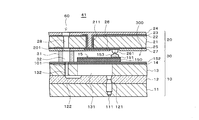
- FIG. 1 is a sectional view showing an example of an ink jet head according to the present invention
- FIG. 2 is a partially enlarged sectional view thereof.
- a head substrate 10 and a wiring substrate 20 each having a rectangular shape in plan view are laminated and integrated via a spacer layer 30 provided therebetween.
- a box-shaped manifold 40 is provided on the upper surface of the wiring board 20, and a liquid storage chamber 41 in which ink is stored is formed between the upper surface of the wiring board 20.
- An ink supply port 42 supplies ink into the liquid storage chamber 41.
- the head substrate 10 includes, from the lower side in the figure, a nozzle plate 11 formed of a Si (silicon) substrate, an intermediate plate 12 formed of a glass substrate, a pressure chamber plate 13 formed of a Si (silicon) substrate, and SiO 2. It has a diaphragm 14 formed of a thin film.
- the nozzle plate 11 includes a nozzle 111 that opens toward the lower surface.
- the pressure chamber plate 13 is formed with a pressure chamber 131 for containing ink for ejection penetrating vertically. Therefore, the upper wall of the pressure chamber 131 is constituted by the diaphragm 14 and the lower wall is constituted by the intermediate plate 12.
- the intermediate plate 12 is formed with a communication passage 121 that allows the inside of the pressure chamber 131 and the nozzle 111 to communicate with each other.
- a piezoelectric element (actuator body) 150 made of a thin film PZT is sandwiched between an upper electrode 151 and a lower electrode 152 which are driving electrodes for driving the piezoelectric element 150.
- the lower electrode 152 is in contact with the surface of the diaphragm 14, and the piezoelectric element 150 and the upper electrode 151 on the upper surface thereof are individually laminated on the lower electrode 152 so as to correspond to the pressure chamber 131 on a one-to-one basis. Has been.
- stud bump 153 is a stud bump, which is formed on the upper electrode 151 with gold or the like and protrudes toward the wiring board 20.
- the stud bump 153 one that does not melt at the temperature of heat treatment such as thermocompression bonding is usually used.
- an upper wiring 23 is formed on the upper surface of a substrate body 21 made of a Si substrate via an insulating layer 22 made of SiO 2 .
- An FPC (flexible printed circuit board) 51 on which a driving IC 50 is mounted is electrically connected to the upper wiring 23 at the end of the wiring board 20 by, for example, ACF (anisotropic conductive film).
- a wiring protection layer 24 made of SiO 2 is laminated on the upper surface of the upper wiring 23.
- a part of the upper wiring 23 faces the lower surface of the substrate body 21 through a through hole 211 formed in the substrate body 21, and a lower portion formed on the lower surface of the substrate body 21 via an insulating layer 25 made of SiO 2. It is electrically connected to the wiring 26.
- a part of the lower wiring 26 is exposed on the wiring protective layer 27 made of SiO 2 facing the actuator 15, and a plurality of, for example, Sn—Bi eutectic solder is formed on the exposed lower wiring 26.
- Solder bumps 261 are formed protruding toward the head substrate 10.
- the spacer layer 30 has a resin portion 31.
- the resin portion 31 is sandwiched between the substrates 10 and 20 so that a predetermined distance is provided between the upper surface of the head substrate 10 and the lower surface of the wiring substrate 20.
- the resin part 31 has a flow path hole 32 penetrating the resin part 31 from the head substrate 10 side to the wiring board 20 side.
- the flow path holes 32 are provided on the upper surface of the head substrate 10 and the ink supply port 201 provided on the lower surface of the wiring substrate 20 at the same time as the head substrate 10 and the wiring substrate 20 are laminated and integrated with the resin portion 31 interposed therebetween. It is provided so as to communicate with the ink introduction port 101 formed.
- the upper end of the flow path hole 32 communicates with the through-hole 28 penetrating the wiring substrate 20 vertically through the ink supply port 201 provided on the lower surface of the wiring substrate 20, and the lower end is the lower electrode 152 of the head substrate 10.
- the pressure chamber plate 13 communicates with a through hole 132 penetrating vertically.
- a communication path 122 that communicates with the inside of the through hole 132 and the pressure chamber 131 is recessed in the surface of the intermediate plate 12 (the bonding surface with the pressure chamber plate 13).
- the holes 32, the through holes 132, and the communication passages 122 constitute individual flow paths 60 for supplying ink from the liquid storage chambers 41 included in the manifold 40 provided on the upper surface of the wiring board 20 to the pressure chambers 131. The That is, one individual flow path 60 passes through one flow path hole 32.
- the resin that forms the resin portion 31 is not particularly limited, but a polyimide resin, an epoxy resin, an acrylic resin, and the like can be preferably exemplified.
- a polyimide resin an epoxy resin, an acrylic resin, and the like can be preferably exemplified.
- the polyimide resin is excellent in rigidity, the distance between the head substrate 10 and the wiring substrate 20 is not particularly limited. It is suitable for uniforming.
- the resin part 31 can be formed by exposure and development using, for example, a thermosetting photosensitive adhesive resin sheet.
- a thermosetting photosensitive adhesive resin sheet include Toray's photosensitive polyimide adhesive sheet and DuPont's PerMX series (trade name).
- the height of the resin part 31 is sufficiently larger than the thickness (height) of the actuator 15. For this reason, a sufficient space is formed between the actuator 15 and the wiring board 20 so as not to hinder the mechanical deformation operation of the actuator 15.
- the spacer layer 30 forms a space portion 300 in a region where the resin portion 31 does not exist.
- Actuators 15 are arranged on the upper surface of the head substrate 10 in the space 300.
- the head substrate 10 and the wiring substrate 20 are both laminated and integrated via the resin portion 31.
- a plurality of stud bumps 153 on the head substrate 10 side and a plurality of solder bumps 261 on the wiring substrate 20 side are provided.
- the space part 300 while making a pair mutually, it is contacting independently of other pairs.
- power can be supplied from the driving IC 50 to the piezoelectric elements 150 from the lower wiring 26 via the upper electrodes 151 of the actuators 15.
- the spacer layer 30 is formed on the wiring substrate 20 side, and the wiring substrate 20 is heat-pressed to the head substrate 10 via the resin portion 31 of the spacer layer 30, thereby both the substrates 10, 20. Are laminated and integrated. That is, the surface of the resin portion 31 of the spacer layer 30 that is oriented to the head substrate 10 is laminated and integrated by pressing and bonding to the head substrate 10.
- the inkjet head 1 has the nozzle 111, the pressure chamber 131, the piezoelectric element 150, the lower wiring 26, and the manifold 40 arranged in a hierarchical structure in the vertical direction. It is planned.
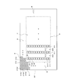
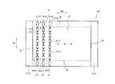
- FIG. 3 is a plan view showing an example of the surface 30 ′ of the spacer layer 30 on the head substrate 10 side. This figure shows the surface of the spacer layer 30 provided on the wiring board 20 side that is oriented to the head substrate 10. However, for convenience of explanation, the wirings provided on the wiring board 20 are not shown here. Only the resin part and the space part are shown.
- a region F surrounded by a broken line is a channel hole arrangement region that includes all of the portions where the plurality of channel holes 32 between the head substrate 10 and the wiring substrate 20 are arranged, and a region B outside the region B. Is a channel hole non-arrangement region where the channel hole 32 is not arranged.
- the channel hole non-arrangement region B is arranged on the outer peripheral side of the spacer layer 30 so as to surround the entire circumference of the channel hole arrangement region F.
- the resin portion 31 in the flow path hole arrangement region F is denoted by 31f
- the resin portion 31 in the flow path hole non-arrangement region B is denoted by 31b.
- 31f ′ is a bonding surface of the resin part 31f to the head substrate 10 in the flow path hole arrangement region F
- 31b ′ is a bonding surface of the resin part 31b to the head substrate 10 in the flow path hole non-arrangement region B.
- the resin surface 31f in the flow path hole arrangement region F has a joining surface 31f 'having a band shape. That is, each of the resin portions 31f is formed in a belt shape having a predetermined width extending along one direction, and an ink flow for individually communicating the ink introduction port 101 of the head substrate 10 and the ink supply port 201 of the wiring substrate 20 respectively.
- a plurality of flow path holes 32 serving as paths are arranged at the same pitch as the arrangement pitch of the pressure chambers along the extending direction of the band shape.
- the bonding surface 31b 'to the head substrate 10 is an aggregate of a large number of circular bonding surfaces 310b'. That is, in the present invention, the resin portion 31 b in the flow path hole non-arrangement region B is formed by a plurality of columns 310 b sandwiched between the head substrate 10 and the wiring substrate 20.
- the plurality of cylinders 310b constituting the resin portion 31b of the flow path hole non-arrangement region B have an interval S between adjacent cylinders 310b.
- the space 300 of the spacer layer 30 communicates from the channel hole arrangement region F to the channel hole non-arrangement region B by providing the gap S.
- each column 310b is easily spread around due to the pressure at the time of thermocompression bonding between the head substrate 10 and the wiring substrate 20, and is thus easily compressed in the height direction. Therefore, even when the head substrate 10 or the wiring substrate 20 has unevenness, warpage, or thickness variation at the time of thermocompression bonding, the resin portion 31b in the channel hole non-arrangement region B is locally compressed according to these distortions. The strain is absorbed.
- the distance between the head substrate 10 and the wiring substrate 20 is made uniform with high accuracy, particularly in the flow path hole arrangement region F.
- the resin portion 31 of the flow path hole arrangement region F having the flow path holes 32 and the bumps 153 and 261 are excessively compressed between the head substrate 10 and the wiring substrate 20, respectively, or used as a counterpart member. It is possible to prevent a portion that cannot be contacted, prevent ink leakage between the substrates 10 and 20, and increase the accuracy of electrical connection.
- the ink jet head of the present invention has an effect of preventing ink ejection failure.
- the resin portion 31b in the flow path hole non-arrangement region B is composed of a plurality of cylinders 310b.
- the present invention is not limited to this, and the resin portion 31b in the flow path hole non-arrangement region B What is necessary is just to consist of the some columnar body 310b.
- the columnar body 310b means a member extending in a columnar shape across both the substrates 10 and 20 in the state before the thermocompression bonding between the head substrate 10 and the wiring substrate 20 in the flow path hole non-arrangement region B.
- a columnar body 310b can preferably be exemplified by prisms such as triangular columns, quadrangular columns, pentagonal columns, hexagonal columns, etc., in addition to the above-described columns.
- a cylinder is preferable.
- the columnar body 310b may be formed in a belt shape connected to the resin portion 31f in the flow path hole arrangement region F.
- the columnar body 310b is a cylinder or a regular polygonal column, the columnar body 310b can be stably crushed in the height direction at the time of thermocompression bonding, so that the arrangement accuracy of the flow path holes 32 and the bumps 153 and 261 is improved, and the inkjet head An effect of further preventing ink discharge failure and further improving ink discharge accuracy can be obtained.
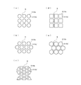
- FIG. 4 is a diagram for explaining an arrangement pattern of the columnar bodies 310b, and is a plan view showing a bonding surface 310b 'of the columnar bodies 310b with respect to the head substrate 10.
- the columnar bodies 310b are arranged in a grid pattern as shown in FIG. 4A, or the columnar bodies 310b are staggered as shown in FIG. 4B.
- the columnar body 310b is a cylinder, but the same applies to other shapes.
- the columnar body 310b is a triangular prism (FIG. 4C), a quadrangular prism (FIG. 4D), or a hexagonal prism (FIG. 4E)
- the prisms 310b are arranged on the side surfaces.
- An arrangement pattern arranged in parallel so as to face each other can be preferably exemplified.
- the respective prisms 310b can be arranged in a state in which the gaps S are provided close to each other.
- the plurality of columnar bodies 310b constituting the resin portion 31b of the flow path hole non-arrangement region B are crushed by joining the head substrate 10 and the wiring substrate 20 to each other. It is also preferable that adjacent columnar bodies 310b are in close contact with each other.
- each cylinder 310b is crushed as shown in FIG. 5 by the pressure during thermocompression bonding. And the adjacent cylinders 310b are connected and are in close contact with each other.
- the columnar body 310b is crushed and the adjacent columnar bodies 310b are brought into close contact with each other by bonding the head substrate 10 and the wiring substrate 20 in this manner, so that the passage hole non-arrangement region
- the resin part 31b of B seals the flow path hole arrangement region F and shields it from the outside air.
- the columnar body 310 b is a cylinder, but the columnar body is the same in other shapes.
- the respective prisms 310b are opposed to each other in parallel.
- the prisms 310b can be arranged in a state of being close to each other. Therefore, by joining the head substrate 10 and the wiring substrate 20, it is possible to suitably form a state in which the adjacent columnar bodies 310 b are connected and in close contact with each other.
- the columnar body 310b constituting the resin portion 31b of the channel hole non-arrangement region B is formed to be hollow inside.
- FIG. 6 is a plan view showing a bonding surface 310b 'of the hollow columnar body 310b with respect to the head substrate 10. As shown in FIG.
- the joint surface 310b 'of the columnar body 310b has a hollow portion M in which no resin is present.
- Forming the hollow portion M in the columnar body 310b is particularly effective when the flow path region F is sealed by bringing the adjacent columnar bodies 310b into close contact with each other, for example, as shown in FIG. That is, when the head substrate 10 and the wiring substrate 20 are thermocompression bonded, the hollow portion M is first sealed by sandwiching the columnar body 310b between the head substrate 10 and the wiring substrate 20. Next, the hollow portion M expands so as to expand the columnar body 310b in the width direction by the temperature of thermocompression bonding. As a result, the close contact between the adjacent columnar bodies 310b is promoted, and the effect that the flow path hole arrangement region F can be suitably sealed is obtained.
- the shape of the resin portion 31f in the flow path hole arrangement region F is not particularly limited, but is preferably a belt-like body extending over the plurality of flow path holes 32 as shown in FIG.
- the case where such a band-shaped bonding surface 31f ′ is pressure-bonded to the head substrate 10 is compared with the case of a discrete bonding surface that is independent for each flow path hole 32 as shown in FIG.
- the resin portion 31b in the channel hole non-arrangement region B absorbs the distortion of the substrates 10 and 20 so as not to disturb the homogenization between the substrates 10 and 20 in the channel hole arrangement region F.
- the distance between the head substrate 10 and the wiring substrate 20 in the channel hole arrangement region F is obtained by the cooperation of the resin portion 31f in the channel hole arrangement region F and the resin portion 31b in the channel hole non-arrangement region B. Can be obtained with the effect of uniformizing with high accuracy.
- the resin portion 31 f in the flow path hole arrangement region F is provided with a side wall portion 33 on both side walls that partially narrows the resin portion 31 f at a position corresponding to the flow path hole 32. It is preferable to have.
- Each of the lightening portions 33 preferably has an arc shape equivalent to a semicircular shape obtained by dividing the flow path hole 32 having a circular opening shape into two along the R1 direction.
- the resin of the resin portion 31f compressed in the height direction at the time of thermocompression bonding between the head substrate 10 and the wiring substrate 20 escapes to the lightening portion 33. This has the effect of preventing the flow passage hole 32 from flowing into the flow passage hole 32 and closing the flow passage hole 32.
- FIG. 7 is a plan view showing another example of the resin portion 31f in the flow path hole arrangement region F.
- FIG. 7 is a plan view showing another example of the resin portion 31f in the flow path hole arrangement region F.
- the resin portion 31 f formed as a band-shaped body can include a notch 34 that linearly crosses the band-shaped body in the band width direction.
- the notch 34 is provided at an intermediate position between the channel holes 32 adjacent to each other in the extending direction of the belt-like body. Further, the notches 34 are formed alternately with the channel holes 32 in the extending direction of the belt-like body. Thereby, the resin part 31f is mutually independent for every flow-path hole 32.
- the resin of the resin portion 31f compressed in the height direction at the time of thermocompression bonding between the head substrate 10 and the wiring substrate 20 is the same as in the case of the above-described cutout portion 33. Since it escapes to the notch part 34, there exists an effect which prevents that excess resin flows into the flow-path hole 32 side and obstruct
- FIG. 1 the resin of the resin portion 31f compressed in the height direction at the time of thermocompression bonding between the head substrate 10 and the wiring substrate 20 is the same as in the case of the above-described cutout portion 33. Since it escapes to the notch part 34, there exists an effect which prevents that excess resin flows into the flow-path hole 32 side and obstruct
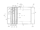
- FIG. 8 is a plan view showing another embodiment of the resin portion 31.
- each of the plurality of resin portions 31 is formed in a belt shape having a predetermined width extending from the channel hole arrangement region F to the channel hole non-arrangement region B along the R1 direction.
- a plurality of flow path holes 32 are arranged at the same pitch as the arrangement pitch of the pressure chambers along the R1 direction.
- the resin portion 31f passing through the flow path hole arrangement region F has the same unit when a resin portion having a predetermined length in the R1 direction including only one flow path hole 32 is defined as one unit resin portion P.
- the resin parts P are repeatedly formed continuously in one direction (R1 direction) from the channel hole arrangement region F to the channel hole non-arrangement region B, so that the channel holes 32 are arranged at a predetermined pitch.
- a single strip-shaped resin portion 31 is formed.
- each unit resin part P constituting each resin part 31 is the same. Therefore, the bonding surfaces 31f ′ and 31b ′ of the resin portions 31 with the head substrate 10 are arranged in one direction so that the planar shape of the unit resin portion P extends from the channel hole arrangement region F to the channel hole non-arrangement region B. It is formed repeatedly.
- the repetition of the unit resin portion P in the channel hole arrangement region F exceeds the boundary with the channel hole non-arrangement region B. This is exactly the same in the channel hole non-arrangement region B.
- the resin part 31b in the flow path hole non-arrangement region B has a gap S between the adjacent resin parts 31b. Therefore, the space portion 300 of the spacer layer 30 communicates from the channel hole arrangement region F to the channel hole non-arrangement region B through the gap S.
- the unit resin portion P is a unit for explaining the continuity of the planar shape of one belt-shaped resin portion 31, and the unit resin portion P is arranged by continuously arranging the unit resin portions P. It does not necessarily mean that the resin part 31 of the book is formed.
- FIG. 1 An enlarged view of one unit resin part P is shown in FIG.
- the unit resin portion P has a lightening portion 33 on both side walls that partially narrows the band width at a position corresponding to the flow path hole 32.
- Each hollow portion 33 has an arc shape equivalent to a semicircular shape obtained by dividing the flow path hole 32 having a circular opening shape into two along the R1 direction.
- the unit resin portion P arranged in the flow passage hole non-arrangement region B also has a hole 32 ′ and a cutout portion 33 ′ having the same shape as the flow passage hole 32 and the cutout portion 33 in exactly the same form. .
- the bonding surfaces 31 f ′ and 31 b ′ a of the resin part 31 with respect to the head substrate 10 extend from the channel hole arrangement region F to the channel hole non-arrangement region B.
- the contact state of the resin portion 31 due to the pressure during the thermocompression bonding between the head substrate 10 and the wiring substrate 20 is made uniform along one direction (R1 direction).
- the resin portion 31 uniformly applies pressure along one direction in the region extending from the channel hole arrangement region F to the channel hole non-arrangement region B. Even if the substrates 10 and 20 are uneven or warped, or the thickness varies, the resin portion 31 can absorb these distortions in the spacer layer 30 with high accuracy.
- the inkjet head 1 is highly accurate electrical connection by the bumps 153 and 261 between both board
- planar shape of the unit resin portion P of the resin portion 31 that is repeatedly formed in one direction is completely the same from the channel hole arrangement region F to the channel hole non-arrangement region B is described.
- planar shape of the bonding surface of the resin part 31 to the head substrate 10 extending from the channel hole arrangement region F to the channel hole non-arrangement region B is substantially the same with a certain width. It may be anything, and is not limited to being completely the same. This will be described below with reference to FIG.
- FIG. 10 is a plan view showing still another example of the spacer layer 30. Parts having the same reference numerals as those in FIG. 8 indicate parts having the same configuration.
- the unit resin portion P of the resin portion 31 passing through the flow path hole arrangement area F has a flow path hole 32 and a lightening part 33 in the flow path hole arrangement area F as in FIG. 8.
- the corresponding holes 32 'and the lightening portions 33' shown in FIG. 8 are not formed. Therefore, the unit resin portion P of each resin portion 31 has a strictly different planar shape in the channel hole arrangement region F and the channel hole non-arrangement region B depending on the presence or absence of the hole and the hollow portion. Become.
- the planar shape of the unit resin portion P includes the presence or absence of a hole 33 ′ corresponding to the flow path hole 32 or the presence or absence of a thinning portion 33 ′ corresponding to the thinning portion 33.
- the channel hole arrangement region F and the channel hole non-arrangement region B are completely identical and repeatedly formed because the effects of the present invention are more remarkably exhibited.
- the flow passage hole non-arrangement region B formed on both outer sides of the flow passage hole arrangement region F perpendicular to the R1 direction is more than the resin portion 31 passing through the flow passage hole arrangement region F.
- a wide band-shaped resin portion 310 is formed along the R1 direction.
- the resin part 310 is not a part that greatly affects the uniformity of the contact state of the resin part 31 along one direction of the R1 direction when the head substrate 10 and the wiring board 20 are thermocompression bonded. Alternatively, it may be formed in the same shape as the belt-shaped resin portion 31 passing through the flow path hole arrangement region F.
- the spacer layer 30 also has a repeated shape that is continuous by the resin portions 31 and 310 from the channel hole arrangement region F to the channel hole non-arrangement region B also in the R2 direction orthogonal to the R1 direction. Therefore, it is preferable because the contact state of the resin portions 31 and 310 can be made uniform along the two directions R1 and R2.
- the bonding surfaces 31 f ′ and 31 b ′ of the resin part 31 with respect to the head substrate 10 move a plurality of unit resin parts P having the same planar shape from the channel hole arrangement region F to the channel hole non-arrangement region B. It is repeatedly formed in two directions (R1 direction and R2 direction).
- the unit resin portions P are continuous with each other in the unit resin portions P adjacent along the R1 direction, and a predetermined gap S and space are provided between the unit resin portions P adjacent along the R2 direction.
- a band-shaped resin portion 31 extending in the R1 direction from the channel hole arrangement region F to the channel hole non-arrangement region B has a gap extending in a band shape.
- S and the space part 300 are sandwiched in the R2 direction. All of the bonding surfaces 31 f ′ and 31 b ′ of the resin part 31 with respect to the head substrate 10 have the same planar shape.
- the hole corresponding to the flow passage hole 32 and the thinning portion corresponding to the thinning portion 33 are provided in the unit resin portion P arranged in the flow passage hole non-arrangement region B.
- the hole 33 ′ and the cutout portion 33 ′ are formed in the same manner as the flow passage hole arrangement region F. May be formed, and is preferred.
- the head substrate 10 and the wiring substrate 20 are obtained by repeating the belt-shaped resin portion 31 extending from the channel hole arrangement region F to the channel hole non-arrangement region B at a predetermined pitch along the R2 direction.
- the spacer layer 30 interposed between the substrates 10 and 20 can absorb the distortion of the head substrate 10 and the wiring substrate 20 with higher accuracy at the time of thermocompression bonding of the ink jet head, thereby preventing the ink ejection failure of the inkjet head more remarkably. There is an effect that can be done.
- the unit resin portion P described above constitutes the belt-shaped resin portion 31 by continuing in one direction. However, as shown in FIG. 12, the unit resin portion P has the same joint surfaces 31f ′ and 31b ′. Adjacent unit resin portions P may be independent from each other as long as the planar shape is.
- each unit resin portion P has a circular shape with the same planar shape of the joint surfaces 31f 'and 31b'.
- the unit flow path part P which has this circular planar shape is the same pitch as the arrangement pitch of the flow path holes 32 in the R1 direction, and extends from the flow path hole arrangement area F to the flow path hole non-arrangement area B. It is formed repeatedly in the direction.
- the unit resin portion P arranged in the channel hole non-arrangement region B does not have a hole corresponding to the channel hole 32 included in the unit resin portion P arranged in the channel hole arrangement region F.
- each unit resin portion P includes only one flow passage hole 32 in the flow passage hole arrangement region F.
- the present invention is not limited to this, and each unit resin portion P is In the channel hole arrangement region F, two or more channel holes 32 may be included.
- each unit resin portion P is repeatedly formed in the R1 direction at a pitch twice the arrangement pitch of the flow path holes 32 in the R1 direction.
- the R1 direction of the channel holes 32 is formed. It can be repeatedly formed in the R1 direction at a pitch n times the arrangement pitch.
- each unit resin portion P shown in FIG. 13 is along R1 direction, and is repeated through the space
- each unit resin portion P is formed so as to include a plurality of flow path holes 32 adjacent along the R2 direction, so that each unit resin portion P has a length direction along the R2 direction.
- the same planar shape may be repeatedly formed in the R2 direction.
- the joint surfaces 31f ′ and 31b ′ of the resin portion 31 are repeatedly formed in an equal area shape at predetermined intervals in at least one direction from the channel hole arrangement region F to the channel hole non-arrangement region B. .
- the repeated portions of the joint surfaces 31f 'and 31b' that are repeatedly formed in at least one direction do not necessarily have the same planar shape, and have an equal area shape that is equal to each other.
- the resin part has a plurality of unit resin parts P ′ each having a joint surface 31 a having an equal area shape, extending from the channel hole arrangement region F to the channel non-arrangement region B in one direction (FIG. 14). (R1 direction in the middle) is formed repeatedly.
- the unit resin portions P ′ having an equal area shape are provided one for each flow path hole 32 in the flow path hole arrangement region F so as to have the same pitch as the arrangement pitch of the flow path holes 32 in the R1 direction. Are repeatedly formed in the R1 direction at predetermined intervals.
- the predetermined interval means that the distance between the center of gravity of the planar shape of the unit resin portion P ′ having the same area shape that is repeated is a predetermined interval.
- the unit resin portion P ′ having an equal area shape is also repeatedly formed in the channel hole non-arrangement region B on the extension line in the repeating direction (R1) in the channel hole arrangement region F.
- the resin portion 31 in the region extending from the flow hole arrangement area F to the non-flow hole arrangement area B between the head substrate 10 and the wiring board 20, the resin portion 31 is subjected to thermocompression bonding.
- the contact state against pressure is made uniform.
- the resin portion 31 can receive pressure uniformly in the region extending from the channel hole arrangement region F to the channel hole non-arrangement region B. Even if the substrates 10 and 20 are uneven or warped, or the thickness varies, the spacer layer 30 can absorb these distortions with high accuracy.
- the wiring 26 and the upper electrode 151 of the piezoelectric element 15 are electrically connected by connecting the stud bump 153 of the head substrate 10 and the solder bump 261 of the wiring substrate 20 has been described.
- the present invention is not limited to the case where bumps are raised from both the head substrate 10 and the wiring substrate 20 as described above.
- the wiring is formed by one bump rising from either the head substrate 10 or the wiring substrate 20. 26 and the upper electrode 151 of the piezoelectric element 15 may be electrically connected.
- the head substrate 10 includes the nozzle 111, the pressure chamber 131, and the piezoelectric element 150
- the wiring substrate 20 includes the lower wiring 26 and is thermocompression bonded via the resin portion 31.
- the present invention is not necessarily limited to this.
- the head substrate 10 and the wiring substrate 20 are thermocompression bonded, for example, when the head substrate 10 does not have the nozzle 111, that is, the nozzle plate 11. This is applicable even when the layer is not yet laminated.
- the present invention can also be applied to the case where the head substrate 10 and the wiring substrate 20 are bonded to each other through the resin portion 31 formed on the substrate.
- the description of the configuration of the surface 30 ′ of the spacer layer 30 on the head substrate 10 side and the bonding surface of the resin portion 31 with respect to the head substrate 10 is made on the surface of the spacer layer 30 on the wiring substrate 20 side and the wiring substrate of the resin portion 31. 20 is used for the configuration of the joint surface with respect to 20.
- Inkjet head 10 Head substrate 101: Ink inlet 11: Nozzle plate 111: Nozzle 112: Liquid channel 12: Intermediate plate 121: Communication channel 122: Communication channel 13: Pressure chamber plate 131: Pressure chamber 132: Through hole 14: Diaphragm 15: Actuator 150: Actuator body (piezoelectric element) 151: Upper electrode 152: Lower electrode 153: Stud bump 20: Wiring board 201: Ink supply port 21: Substrate body 211: Through hole 22: Insulating layer 23: Upper wiring 24: Wiring protective layer 25: Insulating layer 26: Lower wiring 261: Solder bump 27: Wiring protection layer 28: Through hole 30: Spacer layer 30 ': Surface 31, 31f, 31b, 310: Resin part 32: Channel hole 33: Meat cutout part 34: Notch part 300: Space part 310b : Columnar bodies 31f ', 31b', 310b ': Joint surface 40: Manifold 41: Liquid storage chamber 42: Ink supply port 50: Drive
Landscapes
- Particle Formation And Scattering Control In Inkjet Printers (AREA)
Abstract
本発明は、ノズルの高密度化を実現でき且つインク吐出不良を防止できるインクジェットヘッドの提供を目的とし、複数の圧力室、複数の圧電素子、複数の駆動電極、複数のインク導入口を有するヘッド基板と、圧電素子に電力供給する配線、複数のインク供給口を有する配線基板と、ヘッド基板と配線基板とを所定の間隔とするように両基板間に挟設される樹脂部、該樹脂部が存在していない空間部を有するスペーサ層とを備え、ヘッド基板と配線基板は、スペーサ層の樹脂部によって、ヘッド基板と配線基板との間の流路孔が配置される部位を全て含む流路孔配置領域と、該流路孔配置領域を取り囲むように設けられた流路孔が配置されない流路孔非配置領域とに亘って接合されており、流路孔非配置領域における樹脂部は、ヘッド基板と配線基板とに挟設された複数の柱状体によって形成されていることを特徴とする。
Description
本発明は、インクジェットヘッドに関し、詳しくは、ノズルの高密度化を実現でき、且つインク吐出不良を防止できるインクジェットヘッドに関する。
インクジェットヘッドには、インクの共通流路がノズル列毎に設けられる他、インクに吐出圧力を付与するための圧力室や、該圧力室毎に備えられる圧電素子に電力供給するための配線や、共通流路から各圧力室へインクを供給するための個別流路が、複数のノズルに対して個別に設けられるものがある。
近年、このようなインクジェットヘッドにおいても、高精度・高解像度の画像形成を実現するために、複数のノズルを高密度に配置することが要求されている。
このノズルを高密度に配置する要求に対し、特許文献1に記載の液滴吐出ヘッドは、ノズル及び圧力室を有するヘッド基板の上面に樹脂接着部を介して、ヘッド基板に設けられる各圧電素子に電力供給するための配線基板(天板部材)を積層一体化した構成を採用している。
ヘッド基板は、下面から順に、ノズル、圧力室、振動板及び圧電素子を備えている。一方、配線基板は、その下面に、圧力室に液体を供給するためのインク供給口と、圧電素子に設けられる駆動電極に電力供給するための配線を備えてなり、その上面側には、液体プール室が設けられている。液体プール室とインク供給口とは、配線基板を貫通する貫通孔を介して連通している。
ヘッド基板と配線基板とは、間に熱硬化性樹脂を介して加熱圧着することによって接合され、これにより、配線と圧電素子の駆動電極とがバンプによって電気的に接続される。また、同時に、熱硬化性樹脂からなる流路孔を有する隔壁部材によってインク供給口と圧力室とが連通する。
このように、特許文献1では、ノズル、圧力室、振動板、圧電素子、配線、及び液体プール室を、それぞれ上下方向に階層構造となるように配置することによって、ノズルの高密度化を図ることを可能としている。
しかるに、特許文献1に記載のインクジェットヘッドには、インクの吐出不良が生じ易い問題があった。
インクの吐出不良の原因としては、バンプによる電気的な接続の不良、あるいは、隔壁部材におけるインク漏れが考えられる。
従来、このような接続不良は、ヘッド基板と配線基板との間における接着力の不足によって生じるものと考えられてきた。
それ故、本発明者は、ヘッド基板と配線基板との間の接着について、熱硬化性樹脂からなる隔壁部材だけでなく、両部材間の接着のみを目的とする熱硬化性樹脂からなる接着部を、接着力を高めるために比較的広い面積で設けることにより行うことを検討してきた。
これについて図15を参照して説明する。図15は、熱硬化性樹脂を設けたヘッド基板の平面図である。この熱硬化性樹脂は、配線基板に対する接合面を現わしている。
図15において、破線で囲まれる領域Fは、ヘッド基板と配線基板との間において、隔壁部材1001によって形成されるインク流路となる流路孔が配置される部位を全て含む流路孔配置領域であり、その外側に帯状に設けられる領域Bは、流路孔配置領域Fをその全周に亘って取り囲むように設けられ、流路孔が配置されない流路孔非配置領域である。
流路孔配置領域Fに設けられる隔壁部材1001は、高密度に配置される圧電素子1003の形成領域を避けて設ける必要があるため、圧電素子1003が高密度に配置される程小面積となり、通常は流路孔を形成し得るだけの最小限の樹脂によって形成される。そのため、隔壁部材1001におけるヘッド基板又は配線基板に対する接合面積は、同図に示す通り比較的小とされてきた。
これに対して、流路孔非配置領域Bにおいては、流路孔配置領域Fのような制約を受けないため、隔壁部材1001による接合面積を補うように、流路孔非配置領域Bの全面に亘ってベタ状態で接着するための接着部1002が設けられる。つまり、流路孔非配置領域Bの全面は、流路孔配置領域Fを取り囲むように該流路孔配置領域Fの全周に亘って帯状の連続的な接着部1002となる。
従来は、このようにして、ヘッド基板と配線基板との間における接着力を増強して、バンプによる電気的な接続、あるいは、隔壁部材に設けられる流路孔におけるインク漏れを防止する試みがなされてきた。
ところが、このような接着力の増強を図っても、バンプによる電気的な接続、あるいは、隔壁部材におけるインク漏れの防止には限界があった。それ故、従来のインクジェットヘッドは、インクの吐出不良を防止することに限界があった。
バンプによる電気的な接続、あるいは、隔壁部材におけるインク漏れの防止を図るためには、特に、これらが配置される流路孔配置領域Fにおいて、ヘッド基板と配線基板との間の間隔が均一であることが要求される。
しかるに、ヘッド基板や配線基板は、凹凸やソリを生じたり、厚みにバラつきが存在し易いため、熱硬化性樹脂を介して加熱圧着されたヘッド基板と配線基板との間の間隔が不均一となり易いことがわかった。
本発明者は、流路孔配置領域Fにおける両基板間の間隔の均一化のために、流路孔非配置領域Bにおいて熱硬化性樹脂を利用することを試みた。
その結果、流路孔非配置領域Bにおける熱硬化性樹脂を、ヘッド基板と配線基板との間に挟設された複数の柱状体とすることにより、加熱圧着時において、流路孔非配置領域Bにおける熱硬化性樹脂がヘッド基板や配線基板の歪みを精度良く吸収できることを見出し、本発明に至った。
そこで、本発明の課題は、ノズルの高密度化を実現でき、且つインク吐出不良を防止できるインクジェットヘッドを提供することにある。
また本発明の他の課題は、以下の記載によって明らかとなる。
上記課題は、以下の各発明によって解決される。
1. インクを吐出させる複数のノズルにそれぞれ対応して配設され、該ノズルから吐出させるインクを収容する複数の圧力室と、前記圧力室にそれぞれ対応して配置され、該圧力室内のインクを前記ノズルから吐出させるための圧力を付与する複数の圧電素子と、前記圧電素子にそれぞれ対応して設けられた複数の駆動電極と、前記圧力室内へ供給するためのインクを導入する複数のインク導入口とを有するヘッド基板と、
前記駆動電極を介して前記圧電素子にそれぞれ電力供給するための配線と、前記インク導入口へそれぞれインク供給するための複数のインク供給口とを有する配線基板と、
前記ヘッド基板と前記配線基板とを所定の間隔とするように両基板間に挟設される樹脂部と、該樹脂部が存在していない空間部とを有するスペーサ層とを備え、
前記スペーサ層の前記樹脂部を介して前記ヘッド基板と前記配線基板とが圧着されることによって、前記ヘッド基板と前記配線基板とが接合されると共に、前記空間部において前記圧電素子の前記駆動電極と前記配線とが電気的に接続され、且つ前記インク導入口と前記インク供給口とが前記樹脂部の所定位置に設けられた流路孔を介してそれぞれ連通されてなるインクジェットヘッドであって、
前記ヘッド基板と前記配線基板は、前記スペーサ層の前記樹脂部によって、前記ヘッド基板と前記配線基板との間の前記流路孔が配置される部位を全て含む流路孔配置領域と、該流路孔配置領域を取り囲むように設けられた前記流路孔が配置されない流路孔非配置領域とに亘って接合されており、
前記流路孔非配置領域における前記樹脂部は、前記ヘッド基板と前記配線基板とに挟設された複数の柱状体によって形成されていることを特徴とするインクジェットヘッド。
前記駆動電極を介して前記圧電素子にそれぞれ電力供給するための配線と、前記インク導入口へそれぞれインク供給するための複数のインク供給口とを有する配線基板と、
前記ヘッド基板と前記配線基板とを所定の間隔とするように両基板間に挟設される樹脂部と、該樹脂部が存在していない空間部とを有するスペーサ層とを備え、
前記スペーサ層の前記樹脂部を介して前記ヘッド基板と前記配線基板とが圧着されることによって、前記ヘッド基板と前記配線基板とが接合されると共に、前記空間部において前記圧電素子の前記駆動電極と前記配線とが電気的に接続され、且つ前記インク導入口と前記インク供給口とが前記樹脂部の所定位置に設けられた流路孔を介してそれぞれ連通されてなるインクジェットヘッドであって、
前記ヘッド基板と前記配線基板は、前記スペーサ層の前記樹脂部によって、前記ヘッド基板と前記配線基板との間の前記流路孔が配置される部位を全て含む流路孔配置領域と、該流路孔配置領域を取り囲むように設けられた前記流路孔が配置されない流路孔非配置領域とに亘って接合されており、
前記流路孔非配置領域における前記樹脂部は、前記ヘッド基板と前記配線基板とに挟設された複数の柱状体によって形成されていることを特徴とするインクジェットヘッド。
2. 前記スペーサ層の前記空間部は、隣接する前記柱状体間に間隙を有していることにより、前記流路孔配置領域から前記流路孔非配置領域に亘って連通していることを特徴とする前記1記載のインクジェットヘッド。
3. 前記樹脂部の前記ヘッド基板及び/又は前記配線基板に対する接合面が、前記流路孔配置領域から前記流路孔非配置領域に亘って、少なくとも一方向に同一の平面形状で繰り返し形成されていることを特徴とする前記1又は2記載のインクジェットヘッド。
4. 前記平面形状は、隣接する該平面形状同士で互いに連続しており、全体として帯形状を呈していることを特徴とする前記3記載のインクジェットヘッド。
5. 前記樹脂部の前記ヘッド基板及び/又は前記配線基板に対する接合面が、前記流路孔配置領域から前記流路孔非配置領域に亘って、少なくとも1方向に所定の間隔で、等面積形状で繰り返し形成されていることを特徴とする前記1又は2記載のインクジェットヘッド。
6. 前記流路孔非配置領域における前記樹脂部は、前記ヘッド基板と前記配線基板とが接合されることによって前記柱状体が押し潰されて隣接する該柱状体同士が密着しており、前記流路孔配置領域を外気から遮断していることを特徴とする前記1記載のインクジェットヘッド。
7. 前記流路孔配置領域における前記樹脂部は、前記流路孔毎に互いに独立していることを特徴とする前記1~6のいずれかに記載のインクジェットヘッド。
8. 前記流路孔配置領域における前記樹脂部は、前記流路孔の位置で該樹脂部を部分的に細幅とする肉抜き部を有することを特徴とする前記1~7のいずれかに記載のインクジェットヘッド。
9. 前記柱状体は、円柱又は角柱であることを特徴とする前記1~8のいずれかに記載のインクジェットヘッド。
10. 前記樹脂部はポリイミド樹脂からなることを特徴とする前記1~9のいずれかに記載のインクジェットヘッド。
本発明によれば、ノズルの高密度化を実現でき、且つ、インク吐出不良を防止して、インク吐出精度に優れるインクジェットヘッドを提供することができる。
以下、本発明を実施するための形態について図面を用いて説明する。
図1は、本発明に係るインクジェットヘッドの一例を示す断面図であり、図2はその部分拡大断面図である。
インクジェットヘッド1は、それぞれ平面視矩形状のヘッド基板10と配線基板20とが、間に設けられたスペーサ層30を介して積層一体化されている。
配線基板20の上面には箱型形状のマニホールド40が設けられ、配線基板20の上面との間で、内部にインクが貯留される液体貯留室41を形成している。42は、液体貯留室41内にインクを供給するインク供給口である。
ヘッド基板10は、図中下層側から、Si(シリコン)基板によって形成されたノズルプレート11、ガラス基板によって形成された中間プレート12、Si(シリコン)基板によって形成された圧力室プレート13、SiO2薄膜によって形成された振動板14を有している。ノズルプレート11は下面に向かって開口しているノズル111を備えている。
ここでは、圧力室プレート13には、吐出のためのインクを収容する圧力室131が上下に貫通するように形成されている。従って、圧力室131の上壁は振動板14によって構成され、下壁は中間プレート12によって構成されている。中間プレート12には、圧力室131の内部とノズル111とを連通する連通路121が貫通形成されている。
15はアクチュエータであり、薄膜PZTからなる圧電素子(アクチュエータ本体)150が、該圧電素子150を駆動させるための駆動電極である上部電極151と下部電極152とで挟設されてなる。下部電極152は振動板14の表面に接設されており、この下部電極152上に、圧力室131に1対1に対応するように個別に圧電素子150とその上面の上部電極151とが積層されている。
153はスタッドバンプであり、上部電極151上に金等によって形成され、配線基板20に向けて突出形成されている。スタッドバンプ153は、通常、加熱圧着等の加熱処理の温度で融解しないものが用いられる。
配線基板20には、Si基板からなる基板本体21の上面に、SiO2からなる絶縁層22を介して上部配線23が形成されている。この上部配線23には、配線基板20の端部において、駆動IC50が実装されたFPC(フレキシブルプリント回路基板)51が例えばACF(異方性導電フィルム)によって電気的に接続されている。上部配線23の上面には、SiO2からなる配線保護層24が積層されている。
上部配線23の一部は、基板本体21に形成された貫通孔211によって基板本体21の下面に臨んでおり、該基板本体21の下面にSiO2からなる絶縁層25を介して形成された下部配線26と導通している。アクチュエータ15に面するSiO2からなる配線保護層27には、下部配線26の一部が露出しており、その露出した下部配線26に、例えばSn-Bi系共晶はんだによって形成された複数のはんだバンプ261がヘッド基板10に向けて突出形成されている。
スペーサ層30は、樹脂部31を有している。該樹脂部31は、ヘッド基板10の上面と配線基板20の下面との間を所定間隔とするように、両基板10、20間に挟設されている。
また、樹脂部31は、ヘッド基板10側から配線基板20側にかけて該樹脂部31を貫通する流路孔32を有している。
流路孔32は、ヘッド基板10と配線基板20が樹脂部31を挟んで積層一体化されると同時に、配線基板20の下面に設けられたインク供給口201と、ヘッド基板10の上面に設けられたインク導入口101とを連通するように設けられている。
すなわち、流路孔32の上端は、配線基板20の下面に設けられたインク供給口201を通して、配線基板20を上下に貫通する貫通孔28と連通し、下端は、ヘッド基板10の下部電極152及び振動板14を貫通するように形成されたインク導入口101を通して、圧力室プレート13を上下に貫通する貫通孔132と連通している。
さらに、中間プレート12の表面(圧力室プレート13との接合面)には、この貫通孔132と圧力室131の内部と連通する連通路122が凹設されており、これら貫通孔28、流路孔32、貫通孔132及び連通路122によって、配線基板20の上面に設けられたマニホールド40が備える液体貯留室41からのインクを各圧力室131に供給するための個別流路60がそれぞれ構成される。すなわち、一つの個別流路60は一つの流路孔32内を通っている。
樹脂部31を形成する樹脂としては、格別限定されないが、ポリイミド樹脂、エポキシ樹脂、アクリル樹脂等を好ましく例示でき、特にポリイミド樹脂は剛性に優れるため、ヘッド基板10と配線基板20との間の間隔を均一化する上で好適である。
樹脂部31は、例えば熱硬化性の感光性接着樹脂シートを用いて露光、現像によって形成することができる。具体的な感光性接着樹脂シートとしては、例えば東レ社製感光性ポリイミド接着シート、デュポン社製PerMXシリーズ(商品名)等を用いることができる。
樹脂部31の高さは、アクチュエータ15の厚さ(高さ)よりも十分に大きい。このためアクチュエータ15の上方には、配線基板20との間に十分な間隔が形成され、アクチュエータ15の機械的な変形動作を阻害しないようにしている。
スペーサ層30は、ヘッド基板10と配線基板20との間の領域において、樹脂部31が存在していない領域に空間部300を形成している。この空間部300内のヘッド基板10上面に、それぞれアクチュエータ15が配置されている。
ヘッド基板10と配線基板20は、両者が樹脂部31を介して積層一体化されると同時に、ヘッド基板10側の複数のスタッドバンプ153と、配線基板20側の複数のはんだバンプ261とが、空間部300内において、互いに対をなすと共に、他の対とは独立して接触している。これにより、下部配線26から各アクチュエータ15の上部電極151を介して各圧電素子150に駆動IC50からの給電が可能となっている。
ここでは、スペーサ層30を配線基板20側に形成しておき、この配線基板20がスペーサ層30の樹脂部31を介してヘッド基板10に対して加熱圧着されることによって、両基板10、20が積層一体化されている。即ち、スペーサ層30の樹脂部31におけるヘッド基板10に配向する表面を、該ヘッド基板10に圧着して接合することにより、積層一体化されている。
このように、インクジェットヘッド1は、ノズル111、圧力室131、圧電素子150、下部配線26、及び、マニホールド40を、それぞれ上下方向に階層構造となるように配置することにより、ノズル111の高密度化が図られている。
次に、スペーサ層30の詳細について更に説明する。
図3は、スペーサ層30のヘッド基板10側の表面30’の一例を示す平面図である。同図は、配線基板20側に設けられたスペーサ層30のヘッド基板10に配向する面を示しているが、ここでは説明の便宜を図るため、配線基板20に設けられる配線類は図示省略し、樹脂部と空間部のみを示す。
図3において、破線で囲まれる領域Fは、ヘッド基板10と配線基板20との間の複数の流路孔32が配置される部位を全て含む流路孔配置領域であり、その外側の領域Bは、流路孔32が配置されない流路孔非配置領域である。流路孔非配置領域Bは、流路孔配置領域Fの全周を取り囲むように、スペーサ層30における外周側に配置されている。
以下の説明では、流路孔配置領域Fの樹脂部31を31f、流路孔非配置領域Bにおける樹脂部31を31bで示す。
また、31f’は、流路孔配置領域Fにおける樹脂部31fのヘッド基板10に対する接合面であり、31b’は、流路孔非配置領域Bにおける樹脂部31bのヘッド基板10に対する接合面である。
同図に示す通り、流路孔配置領域Fにおける樹脂部31fは、接合面31f’が帯形状を呈している。即ち、樹脂部31fは、それぞれ1方向に沿って延びる所定幅の帯状に形成されており、ヘッド基板10のインク導入口101と配線基板20のインク供給口201とをそれぞれ個別に連通させるインク流路となる複数の流路孔32が、帯形状の延設方向に沿って、圧力室の配列ピッチと同ピッチで配列されている。
一方、流路孔非配置領域Bの樹脂部31bは、ヘッド基板10に対する接合面31b’が多数の円状の接合面310b’の集合体とされている。つまり、本発明において、流路孔非配置領域Bの樹脂部31bは、ヘッド基板10と配線基板20とに挟設された複数の円柱310bから形成されている。
本実施形態においては、流路孔非配置領域Bの樹脂部31bを構成する複数の円柱310bは、隣接する円柱310b間に間隔Sを有している。このため、スペーサ層30の空間部300は、この間隙Sが設けられていることによって、流路孔配置領域Fから流路孔非配置領域Bに亘って連通している。これにより、各々の円柱310bは、ヘッド基板10と配線基板20との加熱圧着時の圧力によって、周囲に広がることが容易となるため、高さ方向に圧縮され易いものとなる。そのため、加熱圧着時に、ヘッド基板10や配線基板20に凹凸やソリ、厚みのバラつきが生じていても、これら歪みに応じて、流路孔非配置領域Bの樹脂部31bが局所的に圧縮され、該歪みを吸収する。このように、流路孔非配置領域Bにおいて基板歪みを吸収することにより、特に流路孔配置領域Fにおいてヘッド基板10と配線基板20との間隔が精度良く均一化される。
これにより、流路孔32を有する流路孔配置領域Fの樹脂部31と、バンプ153、261が、それぞれヘッド基板10と配線基板20との間で、過剰に圧縮されたり、あるいは相手部材に接触できなくなる部分が生じることが防止され、両基板10、20間でのインク漏れが防止され、電気的接続が高精度化される。
これにより、本発明のインクジェットヘッドは、インク吐出不良が防止される効果を奏する。
以上の説明では、流路孔非配置領域Bの樹脂部31bが複数の円柱310bからなる例について説明したが、本発明はこれに限定されず、流路孔非配置領域Bの樹脂部31bが複数の柱状体310bからなるものであればよい。
本発明において柱状体310bとは、流路孔非配置領域Bにおいて、ヘッド基板10と配線基板20との加熱圧着前の状態において、両基板10、20に亘って柱状に延びる部材を意味する。このような柱状体310bは、上述した円柱の他、例えば三角柱、四角柱、五角柱、六角柱等の角柱を好ましく例示できる。特に円柱であることが好ましい。柱状体310bが角柱である場合、柱状体310bは流路孔配置領域F内の樹脂部31fと繋がる帯状に形成されてもよい。
柱状体310bが、円柱や正多角柱であれば、加熱圧着時に高さ方向に安定して押し潰すことができるため、流路孔32やバンプ153、261の配置精度が向上し、インクジェットヘッドのインク吐出不良を更に防止して、インク吐出精度を更に向上する効果が得られる。
また、本発明において、流路孔非配置領域Bの樹脂部31bを構成する多数の柱状体310bは、所定の配置パターンで配置されていることが好ましい。
図4は、柱状体310bの配置パターンを説明する図であり、該柱状体310bのヘッド基板10に対する接合面310b’を示す平面図である。
柱状体310bの配置パターンとしては、図4(a)に示すように柱状体310bを碁盤目状となるように配置したものや、図4(b)に示すように柱状体310bを千鳥状となるように配置したもの等を好ましく例示できる。図示の例では柱状体310bが円柱の場合を示したが、他の形状のものにおいても同様である。
また、柱状体310bが三角柱(図4(c))、四角柱(図4(d))、あるいは六角柱(図4(e))であれば、各々の角柱310b同士を、それぞれの側面を平行に対向させるように並設した配置パターンを好ましく例示できる。このような配置パターンとすることで、各々の角柱310b同士を、間隙Sを設けて互いに近接させた状態で配置させることができる。
また、本発明において、流路孔非配置領域Bの樹脂部31bを構成する複数の柱状体310bは、ヘッド基板10と配線基板20とが接合されることによって該柱状体310bが押し潰されて隣接する柱状体310b同士が密着してなるものであることも好ましい。
つまり、図4(a)のように円柱310bを縦横に碁盤目状に配置した場合を例に説明すると、各々の円柱310bは、加熱圧着時の圧力によって、図5に示すように押し潰されて周囲に広がり、隣接する円柱310b同士が繋がって密着する。
これにより、隣接する円柱310b間の間隙Sに由来して樹脂が存在しない部位Aは、その周囲が樹脂で包囲されると共に上下がヘッド基板10及び配線基板20によって覆われる。従って、流路非配置領域Bにおけるヘッド基板10と配線基板20との間では、樹脂が存在しない部位Aが気泡として規則的に包み込まれる形とされ、樹脂と気泡とがパターン状に配置されるようになる。
本実施形態においては、このように、ヘッド基板10と配線基板20とが接合されることによって柱状体310bが押し潰されて隣接する柱状体310b同士が密着することにより、流路孔非配置領域Bの樹脂部31bが流路孔配置領域Fを密封し、外気から遮断している。
これにより、流路孔配置領域Fの流路孔32を形成する樹脂31f、配線26や圧電素子15、バンプ153、261等が、外気に含まれる水分や酸素等と接触することが防止され、腐食や劣化を防止する効果が得られる。なお、図5の例では柱状体310bが円柱の場合を示したが、柱状体は他の形状の場合も同様である。
例えば、図4(c)~(e)に示したように、柱状体310bが三角柱、四角柱、又は六角柱の場合であれば、各々の角柱310b同士を、それぞれの側面を平行に対向させるように並設した配置パターンとすることで、各々の角柱310b同士を、互いに近接させた状態で配置することができる。そのため、ヘッド基板10と配線基板20とが接合されることによって、隣接する柱状体310b同士が繋がって密着される状態を好適に形成することができる。
本発明において、流路孔非配置領域Bの樹脂部31bを構成する柱状体310bは、内部が中空状に形成されることも好ましいことである。
図6は、中空状の柱状体310bのヘッド基板10に対する接合面310b’を示す平面図である。
図6に示す通り、柱状体310bの接合面310b’は、その内部に樹脂が存在していない中空部Mを有している。
柱状体310bに中空部Mを形成することは、例えば図5に示したように、隣接する柱状体310b同士を密着させて流路領域Fを密封する場合に特に効果的である。すなわち、ヘッド基板10と配線基板20との加熱圧着時に、柱状体310bがヘッド基板10と配線基板20とに挟設されることによって、まず中空部Mが密封される。次いで加熱圧着の温度によって中空部Mが柱状体310bを幅方向に拡張するように膨張する。これにより、隣接する柱状体310b同士の密着が促進され、流路孔配置領域Fを好適に密封することが可能となる効果が得られる。
図6の例では、柱状体310bが円柱の場合について示したが、他の形状の柱状体であっても中空部Mを有することにより同様の効果が得られる。
本発明において、流路孔配置領域Fにおける樹脂部31fの形状は格別限定されないが、図3に示したように、複数の流路孔32に跨る帯状体とすることが好ましい。
本発明において、このような帯状の接合面31f’によってヘッド基板10に圧着される場合は、例えば図15に示したような流路孔32毎に独立した不連続な接合面の場合と比較して、ヘッド基板10と配線基板20との加熱圧着時においてヘッド基板10に対する接触が安定し、ヘッド基板10と配線基板20との間の間隔が均一化されやすい。このとき、流路孔非配置領域Bの樹脂部31bは、流路孔配置領域Fにおける両基板10、20間の均一化を妨げないように、各基板10、20の歪みを吸収する。つまり、流路孔配置領域Fの樹脂部31fと流路孔非配置領域Bの樹脂部31bとが協働して、流路孔配置領域Fにおけるヘッド基板10と配線基板20との間の間隔を高精度に均一化する効果が得られる。
流路孔配置領域Fにおける樹脂部31fには、図3に示したように、流路孔32に対応する位置で該樹脂部31fを部分的に細幅とする肉抜き部33を両側壁面に有していることが好ましい。各肉抜き部33は、開口形状が円形状となる流路孔32を、R1方向に沿って2分割した半円形状と同等の円弧形状を呈していることが好ましい。
このような肉抜き部33を設けることにより、ヘッド基板10と配線基板20との加熱圧着時において高さ方向に圧縮された樹脂部31fの樹脂が該肉抜き部33に逃げるため、過剰な樹脂が流路孔32側に流入して該流路孔32を閉塞することが防止される効果を奏する。
更に、図7は、流路孔配置領域Fにおける樹脂部31fの他の例を示す平面図である。
図7に示すように、帯状体として形成された樹脂部31fは、帯幅方向に該帯状体を直線状に横断する切欠部34を備えることができる。切欠部34は、帯状体の延設方向に互いに隣接する流路孔32間の中間位置に設けられている。また、切欠部34は、帯状体の延設方向において、流路孔32と交互に形成されている。これにより、樹脂部31fは、流路孔32毎に互いに独立している。
このような切欠部34を設けることにより、前述した肉抜き部33の場合と同様に、ヘッド基板10と配線基板20との加熱圧着時において高さ方向に圧縮された樹脂部31fの樹脂が該切欠部34に逃げるため、過剰な樹脂が流路孔32側に流入して該流路孔32を閉塞することが防止される効果を奏する。
図8は、樹脂部31の他の実施形態を示す平面図である。
同図に示す通り、複数の樹脂部31は、それぞれR1方向に沿って流路孔配置領域Fから流路孔非配置領域Bに亘って延びる所定幅の帯状に形成されており、そのうち流路孔配置領域F内を通る樹脂部31fには、複数の流路孔32が、R1方向に沿って、圧力室の配列ピッチと同ピッチで配列されている。
ここで、流路孔配置領域F内を通る樹脂部31fは、1つだけの流路孔32を含むR1方向に所定長さの樹脂部分を一つの単位樹脂部Pとした時、同一の単位樹脂部Pが、流路孔配置領域Fから流路孔非配置領域Bに亘って、1方向(R1方向)に連続して繰り返し形成されることで、流路孔32が所定ピッチで配列された1本の帯状の樹脂部31を構成している。
各樹脂部31を構成する各単位樹脂部Pの平面形状はいずれも同一である。従って、各樹脂部31におけるヘッド基板10との接合面31f’、31b’は、単位樹脂部Pの平面形状が、流路孔配置領域Fから流路孔非配置領域Bに亘って、1方向に繰り返し形成されていることになる。
この流路孔配置領域Fから流路孔非配置領域Bに亘ってとは、流路孔配置領域Fにおける単位樹脂部Pの繰り返しが、流路孔非配置領域Bとの境界を越えて該流路孔非配置領域B内においても全く同様に繰り返されていることである。これにより、流路孔非配置領域Bにおける樹脂部31bは、隣接する樹脂部31b間に間隙Sを有している。従って、スペーサ層30の空間部300は、この間隙Sによって、流路孔配置領域Fから流路孔非配置領域Bに亘って連通している。
なお、ここでいう単位樹脂部Pは、帯状の1本の樹脂部31の平面形状の連続性を説明するための単位であって、この単位樹脂部Pを連続して並設することによって1本の樹脂部31を形成することを必ずしも意味するものではない。
1つの単位樹脂部Pの拡大図を図9に示す。
同図に示すように、単位樹脂部Pは、流路孔32に対応する位置で帯幅を部分的に細幅とする肉抜き部33を両側壁面に有している。各肉抜き部33は、開口形状が円形状となる流路孔32を、R1方向に沿って2分割した半円形状と同等の円弧形状を呈している。このような肉抜き部33を設けることにより、ヘッド基板10と配線基板20との加熱圧着時において高さ方向に圧縮された樹脂部31の樹脂が該肉抜き部33に逃げるため、流路孔配置領域Fにおいて過剰な樹脂が流路孔32側に流入して該流路孔32を閉塞することが防止される効果を奏する。
流路孔非配置領域B内に配置される単位樹脂部Pも、流路孔32及び肉抜き部33と同形状の孔32’及び肉抜き部33’を全く同様の形態で有している。
この実施形態においては、図8に示した通り、樹脂部31のヘッド基板10に対する接合面31f’、31b’aが、流路孔配置領域Fから流路孔非配置領域Bに亘って、単位樹脂部Pの繰り返しによって1方向に同一の平面形状で繰り返し形成されていることにより、ヘッド基板10と配線基板20との間の流路孔配置領域Fから流路孔非配置領域Bに亘る領域で、ヘッド基板10と配線基板20との加熱圧着時の圧力による樹脂部31の接触状態が、1方向(R1方向)に沿って均一化される。
特に、隣接する帯状の樹脂部31の間は所定の間隙Sを有し、流路孔配置領域Fから流路孔非配置領域Bに亘って空間部300が連通しているため、樹脂部31の部分的な圧力のばらつきを、樹脂部31が局部的に変形することによって、この複数の樹脂部31の並設方向(R1方向と直交するR2方向)に逃がすことができる。
その結果、ヘッド基板10と配線基板20との加熱圧着時において、流路孔配置領域Fから流路孔非配置領域Bに亘る領域で、1方向に沿って、樹脂部31が圧力を均一に受けることができ、各基板10、20に凹凸やソリが生じていたり、厚みにバラつきが存在していたりしても、スペーサ層30において樹脂部31がこれらの歪みを精度良く吸収できる。
これにより、インクジェットヘッド1は、ヘッド基板10と配線基板20との間の間隔が精度良く均一化されるので、両基板10、20間でのバンプ153、261による高精度な電気的な接続、あるいは、流路孔32におけるインク漏れの防止が図られ、インク吐出不良を顕著に防止できる効果を奏する。
以上の説明では、1方向に繰り返し形成される樹脂部31の単位樹脂部Pの平面形状が、流路孔配置領域Fから流路孔非配置領域Bに亘って完全に同一となる場合について説明したが、流路孔配置領域Fから流路孔非配置領域Bに亘る樹脂部31のヘッド基板10に対する接合面の平面形状が同一であるとは、平面形状がある程度の幅をもって実質的に等しいものであればよく、完全に同一であるものに限らない。これについて、以下に図10を参照して説明する。
図10は、スペーサ層30の更に他の一例を示す平面図である。図8と同一符号の部位は同一構成の部位を示している。
図10において、流路孔配置領域Fを通る樹脂部31の単位樹脂部Pは、流路孔配置領域F内においては、図8と同様に流路孔32及び肉抜き部33を有しているが、流路孔非配置領域Bにおいては、これらに対応する図8に示されていた孔32’及び肉抜き部33’は形成されていない。従って、各樹脂部31の単位樹脂部Pは、この孔及び肉抜き部の有無によって、流路孔配置領域F内と流路孔非配置領域B内とで平面形状が厳密には異なることになる。
しかし、これら孔及び肉抜き部は、接合面31f’の平面形状からすれば極めて微小な部位であり、各樹脂部31は、R1方向に沿って、流路孔配置領域Fから流路孔非配置領域Bに亘って、肉抜き部の部位以外の帯幅が同幅の帯状で連続しているため、実質的に同一の平面形状と看做すことができる。このため、孔及び肉抜き部の有無はほぼ無視することができ、上記同様の効果を得ることができる。
但し、図8に示したように、単位樹脂部Pの平面形状は、流路孔32に対応した孔33’の有無、あるいは、肉抜き部33に対応した肉抜き部33’の有無を含めて、流路孔配置領域Fと流路孔非配置領域Bとで互いに完全に同一で繰り返し形成される場合は、本発明の効果をより顕著に奏することになるため好ましい。
図8、図10に示す態様では、R1方向と直交する流路孔配置領域Fの両外側に形成される流路孔非配置領域Bには、流路孔配置領域Fを通る樹脂部31よりも幅広の帯状の樹脂部310がR1方向に沿ってそれぞれ形成されている。この樹脂部310は、ヘッド基板10と配線基板20との加熱圧着時におけるR1方向の1方向に沿う樹脂部31の接触状態の均一化に大きな影響を及ぼす部位ではないが、この樹脂部310も、流路孔配置領域F内を通る帯状の樹脂部31と同形状に形成してもよい。
このようにすれば、R1方向と直交するR2方向においても、スペーサ層30は、流路孔配置領域Fから流路孔非配置領域Bに亘って、樹脂部31、310によって連続した繰り返し形状となるため、R1及びR2の2方向に沿って、樹脂部31、310の接触状態の均一化を図ることができるために好ましい。
この態様を図11に示す。図10と同一符号の部位は同一構成の部位を示している。
図11において、樹脂部31のヘッド基板10に対する接合面31f’、31b’は、同一の平面形状を有する複数の単位樹脂部Pを、流路孔配置領域Fから流路孔非配置領域Bに亘って、2方向(R1方向及びR2方向)にそれぞれ繰り返し形成している。
ここでは、単位樹脂部Pは、R1方向に沿って隣接する単位樹脂部P同士で互いに連続しており、R2方向に沿って隣接する単位樹脂部P同士では、間に所定の間隙S及び空間部300を介して互いに独立しており、全体として、流路孔配置領域Fから流路孔非配置領域Bに亘って、R1方向に延設された帯状の樹脂部31が、帯状に延びる間隙S及び空間部300を挟んでR2方向に並設された形態を呈している。そして、樹脂部31のヘッド基板10に対する接合面31f’、31b’の全てが、同一の平面形状となっている。
図11では、図10の場合と同様に、流路孔非配置領域B内に配置される単位樹脂部Pにおいて、流路孔32に対応する孔及び肉抜き部33に対応する肉抜き部が形成されていないが、図8の場合と同様に、流路孔非配置領域B内に配置される単位樹脂部Pにおいても流路孔配置領域Fと同様に孔33’及び肉抜き部33’が形成されていてもよく、また好ましい。
このように、流路孔配置領域Fから流路孔非配置領域Bに亘って延びる帯状の樹脂部31を、R2方向に沿って所定のピッチで繰り返すことによって、ヘッド基板10と配線基板20との加熱圧着時において、両基板10、20間に介層されるスペーサ層30が、ヘッド基板10や配線基板20の歪みを更に精度良く吸収できるため、インクジェットヘッドのインク吐出不良を更に顕著に防止できる効果を奏する。
以上説明した単位樹脂部Pは1方向に連続することによって帯状の樹脂部31を構成するようにしたが、図12に示す通り、単位樹脂部Pは、接合面31f’、31b’が互いに同一の平面形状であれば、隣接する単位樹脂部P同士が互いに独立していてもよい。
図12に示す例において、各単位樹脂部Pは、接合面31f’、31b’の平面形状が同一の円形状を呈している。そして、この円形の平面形状を有する単位流路部Pが、流路孔32のR1方向の配列ピッチと同じピッチで、流路孔配置領域Fから流路孔非配置領域Bに亘って、R1方向に繰り返し形成されている。
図示の例は、流路孔非配置領域Bに配置される単位樹脂部Pは、流路孔配置領域Fに配置される単位樹脂部Pが有する流路孔32に対応する孔を有さない場合であるが、流路孔非配置領域Bに配置される単位樹脂部Pにも流路孔32に対応する孔を備えることは好ましいことである。
以上の説明では、各単位樹脂部Pが、流路孔配置領域Fにおいて流路孔32を1つだけ含む場合について説明したが、これに限定されるものではなく、各単位樹脂部Pは、流路孔配置領域Fにおいて2以上の複数の流路孔32を含むものとすることもできる。
図13の例では、同一の平面形状を有する複数の単位樹脂部Pが、流路孔配置領域Fにおいて、R1方向に隣接する2つの流路孔32をそれぞれ含むように形成されている。ここでは、各単位樹脂部Pは、流路孔32のR1方向の配列ピッチの2倍のピッチで、R1方向に繰り返し形成されている。
これと同様にして、同一の平面形状を有する複数の単位樹脂部Pは、R1方向に隣接するn個の流路孔32をそれぞれ含むように形成される場合は、流路孔32のR1方向の配列ピッチのn倍のピッチで、R1方向に繰り返し形成することができる。
なお、図13に示す各単位樹脂部Pの長さ方向は、R1方向に沿っており、R2方向には、間に間隙S及び空間部300を介して繰り返されている。しかし、この態様において、各単位樹脂部Pは、R2方向に沿って隣接する複数の流路孔32を含むように形成することで、長さ方向がR2方向に沿うように各単位樹脂部Pを配置し、該R2方向に同一の平面形状が繰り返し形成されるようにしてもよい。
次に、樹脂部31のヘッド基板10に対する接合面31f’、31b’の他の態様を図14に示す。
この樹脂部31の接合面31f’、31b’は、流路孔配置領域Fから流路孔非配置領域Bに亘って、少なくとも1方向に所定の間隔で、等面積形状で繰り返し形成されている。
つまり、この態様では、少なくとも1方向に繰り返し形成される接合面31f’、31b’の繰り返し部位が、必ずしも同一の平面形状である必要はなく、互いに等面積である等面積形状とされる。
図14に示す通り、樹脂部は、接合面31aがそれぞれ等面積形状である複数の単位樹脂部P’を、流路孔配置領域Fから流路非配置領域Bに亘って、1方向(図中R1方向)に繰り返し形成することによって構成されている。
等面積形状である単位樹脂部P’は、流路孔配置領域Fにおいて1つの流路孔32毎に1つずつ付与され、流路孔32のR1方向の配列ピッチと同じピッチとなるように、所定の間隔でR1方向に繰り返し形成されている。この態様において、所定の間隔とは、繰り返される等面積形状の単位樹脂部P’の平面形状の重心間距離が所定の間隔であることを意味する。
等面積形状となる単位樹脂部P’は、流路孔配置領域Fにおける繰り返し方向(R1)の延長線上にある流路孔非配置領域Bにおいても繰り返し形成されている。
この態様においては、上述した態様と同様に、ヘッド基板10と配線基板20との間の流路孔配置領域Fから流路孔非配置領域Bに亘る領域で、樹脂部31の加熱圧着時の圧力に対する接触状態が均一化される。その結果、ヘッド基板10と配線基板20との加熱圧着時において、流路孔配置領域Fから流路孔非配置領域Bに亘る領域で、樹脂部31が圧力を均一に受けることができ、各基板10、20に凹凸やソリが生じていたり、厚みにバラつきが存在していたりしても、スペーサ層30が、これらの歪みを精度良く吸収できる。
以上の説明では、ヘッド基板10のスタッドバンプ153と配線基板20のはんだバンプ261とを接続することにより、配線26と圧電素子15の上部電極151との電気的な接続が行われる例について説明したが、本発明はこのようにヘッド基板10と配線基板20の両方からバンプを立ち上げるものに限定されず、例えば、ヘッド基板10又は配線基板20の何れか片方から立ち上がった1つのバンプによって、配線26と圧電素子15の上部電極151との電気的な接続が行われるものであってもよい。
また、以上の説明では、ヘッド基板10が、ノズル111と、圧力室131と、圧電素子150とを有し、配線基板20が、下部配線26を有する状態で、樹脂部31を介して加熱圧着される場合について説明したが、本発明は必ずしもこれに限定されず、ヘッド基板10と配線基板20との加熱圧着時において、例えばヘッド基板10がノズル111を有さない場合、つまり、ノズルプレート11が未だ積層されていない場合であっても適用できる。
更に、以上の説明では、配線基板20に形成された樹脂部31を介してヘッド基板10と配線基板20とが接着される場合について説明したが、本発明はこれに限定されず、ヘッド基板10に形成された樹脂部31を介してヘッド基板10と配線基板20とが接着される場合にも適用できる。この場合、スペーサ層30のヘッド基板10側の表面30’及び樹脂部31のヘッド基板10に対する接合面の構成についてした説明が、スペーサ層30の配線基板20側の表面及び樹脂部31の配線基板20に対する接合面の構成に援用される。
1:インクジェットヘッド
10:ヘッド基板
101:インク導入口
11:ノズルプレート
111:ノズル
112:液体流路
12:中間プレート
121:連通路
122:連通路
13:圧力室プレート
131:圧力室
132:貫通孔
14:振動板
15:アクチュエータ
150:アクチュエータ本体(圧電素子)
151:上部電極
152:下部電極
153:スタッドバンプ
20:配線基板
201:インク供給口
21:基板本体
211:貫通孔
22:絶縁層
23:上部配線
24:配線保護層
25:絶縁層
26:下部配線
261:はんだバンプ
27:配線保護層
28:貫通孔
30:スペーサ層
30’:表面
31、31f、31b、310:樹脂部
32:流路孔
33:肉抜き部
34:切欠部
300:空間部
310b:柱状体
31f’、31b’、310b’:接合面
40:マニホールド
41:液体貯留室
42:インク供給口
50:駆動IC
51:FPC
60:個別流路
F:流路孔配置領域
B:流路孔非配置領域
S:間隙
P、P’:単位樹脂部
10:ヘッド基板
101:インク導入口
11:ノズルプレート
111:ノズル
112:液体流路
12:中間プレート
121:連通路
122:連通路
13:圧力室プレート
131:圧力室
132:貫通孔
14:振動板
15:アクチュエータ
150:アクチュエータ本体(圧電素子)
151:上部電極
152:下部電極
153:スタッドバンプ
20:配線基板
201:インク供給口
21:基板本体
211:貫通孔
22:絶縁層
23:上部配線
24:配線保護層
25:絶縁層
26:下部配線
261:はんだバンプ
27:配線保護層
28:貫通孔
30:スペーサ層
30’:表面
31、31f、31b、310:樹脂部
32:流路孔
33:肉抜き部
34:切欠部
300:空間部
310b:柱状体
31f’、31b’、310b’:接合面
40:マニホールド
41:液体貯留室
42:インク供給口
50:駆動IC
51:FPC
60:個別流路
F:流路孔配置領域
B:流路孔非配置領域
S:間隙
P、P’:単位樹脂部
Claims (10)
- インクを吐出させる複数のノズルにそれぞれ対応して配設され、該ノズルから吐出させるインクを収容する複数の圧力室と、前記圧力室にそれぞれ対応して配置され、該圧力室内のインクを前記ノズルから吐出させるための圧力を付与する複数の圧電素子と、前記圧電素子にそれぞれ対応して設けられた複数の駆動電極と、前記圧力室内へ供給するためのインクを導入する複数のインク導入口とを有するヘッド基板と、
前記駆動電極を介して前記圧電素子にそれぞれ電力供給するための配線と、前記インク導入口へそれぞれインク供給するための複数のインク供給口とを有する配線基板と、
前記ヘッド基板と前記配線基板とを所定の間隔とするように両基板間に挟設される樹脂部と、該樹脂部が存在していない空間部とを有するスペーサ層とを備え、
前記スペーサ層の前記樹脂部を介して前記ヘッド基板と前記配線基板とが圧着されることによって、前記ヘッド基板と前記配線基板とが接合されると共に、前記空間部において前記圧電素子の前記駆動電極と前記配線とが電気的に接続され、且つ前記インク導入口と前記インク供給口とが前記樹脂部の所定位置に設けられた流路孔を介してそれぞれ連通されてなるインクジェットヘッドであって、
前記ヘッド基板と前記配線基板は、前記スペーサ層の前記樹脂部によって、前記ヘッド基板と前記配線基板との間の前記流路孔が配置される部位を全て含む流路孔配置領域と、該流路孔配置領域を取り囲むように設けられた前記流路孔が配置されない流路孔非配置領域とに亘って接合されており、
前記流路孔非配置領域における前記樹脂部は、前記ヘッド基板と前記配線基板とに挟設された複数の柱状体によって形成されていることを特徴とするインクジェットヘッド。 - 前記スペーサ層の前記空間部は、隣接する前記柱状体間に間隙を有していることにより、前記流路孔配置領域から前記流路孔非配置領域に亘って連通していることを特徴とする請求項1記載のインクジェットヘッド。
- 前記樹脂部の前記ヘッド基板及び/又は前記配線基板に対する接合面が、前記流路孔配置領域から前記流路孔非配置領域に亘って、少なくとも一方向に同一の平面形状で繰り返し形成されていることを特徴とする請求項1又は2記載のインクジェットヘッド。
- 前記平面形状は、隣接する該平面形状同士で互いに連続しており、全体として帯形状を呈していることを特徴とする請求項3記載のインクジェットヘッド。
- 前記樹脂部の前記ヘッド基板及び/又は前記配線基板に対する接合面が、前記流路孔配置領域から前記流路孔非配置領域に亘って、少なくとも1方向に所定の間隔で、等面積形状で繰り返し形成されていることを特徴とする請求項1又は2記載のインクジェットヘッド。
- 前記流路孔非配置領域における前記樹脂部は、前記ヘッド基板と前記配線基板とが接合されることによって前記柱状体が押し潰されて隣接する該柱状体同士が密着しており、前記流路孔配置領域を外気から遮断していることを特徴とする請求項1記載のインクジェットヘッド。
- 前記流路孔配置領域における前記樹脂部は、前記流路孔毎に互いに独立していることを特徴とする請求項1~6のいずれかに記載のインクジェットヘッド。
- 前記流路孔配置領域における前記樹脂部は、前記流路孔の位置で該樹脂部を部分的に細幅とする肉抜き部を有することを特徴とする請求項1~7のいずれかに記載のインクジェットヘッド。
- 前記柱状体は、円柱又は角柱であることを特徴とする請求項1~8のいずれかに記載のインクジェットヘッド。
- 前記樹脂部はポリイミド樹脂からなることを特徴とする請求項1~9のいずれかに記載のインクジェットヘッド。
Applications Claiming Priority (4)
| Application Number | Priority Date | Filing Date | Title |
|---|---|---|---|
| JP2011-119726 | 2011-05-27 | ||
| JP2011119726 | 2011-05-27 | ||
| JP2011137889 | 2011-06-21 | ||
| JP2011-137889 | 2011-06-21 |
Publications (1)
| Publication Number | Publication Date |
|---|---|
| WO2012165322A1 true WO2012165322A1 (ja) | 2012-12-06 |
Family
ID=47259179
Family Applications (1)
| Application Number | Title | Priority Date | Filing Date |
|---|---|---|---|
| PCT/JP2012/063456 Ceased WO2012165322A1 (ja) | 2011-05-27 | 2012-05-25 | インクジェットヘッド |
Country Status (2)
| Country | Link |
|---|---|
| JP (1) | JPWO2012165322A1 (ja) |
| WO (1) | WO2012165322A1 (ja) |
Citations (3)
| Publication number | Priority date | Publication date | Assignee | Title |
|---|---|---|---|---|
| JPH10166596A (ja) * | 1996-12-06 | 1998-06-23 | Seiko Precision Kk | インクジェットヘッドの製造方法 |
| JP2007083484A (ja) * | 2005-09-21 | 2007-04-05 | Fuji Xerox Co Ltd | 液滴吐出ヘッド、及び、液滴吐出ヘッド製造方法 |
| JP2010221434A (ja) * | 2009-03-19 | 2010-10-07 | Seiko Epson Corp | 液体噴射ヘッド及びその製造方法並びに液体噴射装置 |
-
2012
- 2012-05-25 WO PCT/JP2012/063456 patent/WO2012165322A1/ja not_active Ceased
- 2012-05-25 JP JP2013518048A patent/JPWO2012165322A1/ja active Pending
Patent Citations (3)
| Publication number | Priority date | Publication date | Assignee | Title |
|---|---|---|---|---|
| JPH10166596A (ja) * | 1996-12-06 | 1998-06-23 | Seiko Precision Kk | インクジェットヘッドの製造方法 |
| JP2007083484A (ja) * | 2005-09-21 | 2007-04-05 | Fuji Xerox Co Ltd | 液滴吐出ヘッド、及び、液滴吐出ヘッド製造方法 |
| JP2010221434A (ja) * | 2009-03-19 | 2010-10-07 | Seiko Epson Corp | 液体噴射ヘッド及びその製造方法並びに液体噴射装置 |
Also Published As
| Publication number | Publication date |
|---|---|
| JPWO2012165322A1 (ja) | 2015-02-23 |
Similar Documents
| Publication | Publication Date | Title |
|---|---|---|
| US8322823B2 (en) | Liquid ejecting head, manufacturing method thereof, and liquid ejecting apparatus | |
| US9573371B2 (en) | Head and liquid ejecting apparatus | |
| US9914300B2 (en) | Head and liquid ejecting apparatus with electrically connecting bumps | |
| JP4333584B2 (ja) | インクジェットヘッド | |
| JP4973470B2 (ja) | 圧電アクチュエータ | |
| JP6711047B2 (ja) | 圧電デバイス、液体噴射ヘッド及び液体噴射装置 | |
| WO2011132516A1 (ja) | インクジェット式記録ヘッド | |
| JP2016034740A (ja) | 液体噴射ヘッドおよび液体噴射装置 | |
| JP2014162085A (ja) | 液体吐出装置及びフレキシブル配線基板の接続方法 | |
| US10220619B2 (en) | MEMS device, head and liquid jet device | |
| JP2015160339A (ja) | 配線実装構造、液体噴射ヘッド及び液体噴射装置 | |
| JP4259542B2 (ja) | インクジェットヘッド | |
| JP2007268849A (ja) | インクジェットヘッド及びその製造方法 | |
| JP5633342B2 (ja) | 液体吐出ヘッドの製造方法、及び、液体吐出ヘッド | |
| WO2012165322A1 (ja) | インクジェットヘッド | |
| JP4315236B2 (ja) | インクジェットヘッド | |
| JP6217448B2 (ja) | 液体吐出装置及び圧電アクチュエータ | |
| US7922304B2 (en) | Liquid droplet jetting head | |
| JP5157989B2 (ja) | 圧電アクチュエータとこれを用いた液滴吐出ヘッド | |
| JP6330819B2 (ja) | 配線基板及びインクジェットヘッド | |
| JP2006205670A (ja) | インクジェットヘッド | |
| JP5146381B2 (ja) | 液体吐出装置 | |
| JP2011218641A (ja) | インクジェットヘッド | |
| US12319058B2 (en) | Liquid ejection recording element unit and method for producing same | |
| JP2012126028A (ja) | インクジェットヘッドユニット |
Legal Events
| Date | Code | Title | Description |
|---|---|---|---|
| 121 | Ep: the epo has been informed by wipo that ep was designated in this application |
Ref document number: 12793831 Country of ref document: EP Kind code of ref document: A1 |
|
| ENP | Entry into the national phase |
Ref document number: 2013518048 Country of ref document: JP Kind code of ref document: A |
|
| NENP | Non-entry into the national phase |
Ref country code: DE |
|
| 122 | Ep: pct application non-entry in european phase |
Ref document number: 12793831 Country of ref document: EP Kind code of ref document: A1 |