WO2012161265A1 - 半導体薄膜結晶の製造方法および装置 - Google Patents
半導体薄膜結晶の製造方法および装置 Download PDFInfo
- Publication number
- WO2012161265A1 WO2012161265A1 PCT/JP2012/063352 JP2012063352W WO2012161265A1 WO 2012161265 A1 WO2012161265 A1 WO 2012161265A1 JP 2012063352 W JP2012063352 W JP 2012063352W WO 2012161265 A1 WO2012161265 A1 WO 2012161265A1
- Authority
- WO
- WIPO (PCT)
- Prior art keywords
- thin film
- substrate
- gas
- germanium
- film
- Prior art date
- Legal status (The legal status is an assumption and is not a legal conclusion. Google has not performed a legal analysis and makes no representation as to the accuracy of the status listed.)
- Ceased
Links
Images



Classifications
-
- H—ELECTRICITY
- H10—SEMICONDUCTOR DEVICES; ELECTRIC SOLID-STATE DEVICES NOT OTHERWISE PROVIDED FOR
- H10P—GENERIC PROCESSES OR APPARATUS FOR THE MANUFACTURE OR TREATMENT OF DEVICES COVERED BY CLASS H10
- H10P14/00—Formation of materials, e.g. in the shape of layers or pillars
- H10P14/20—Formation of materials, e.g. in the shape of layers or pillars of semiconductor materials
- H10P14/24—Formation of materials, e.g. in the shape of layers or pillars of semiconductor materials using chemical vapour deposition [CVD]
-
- C—CHEMISTRY; METALLURGY
- C30—CRYSTAL GROWTH
- C30B—SINGLE-CRYSTAL GROWTH; UNIDIRECTIONAL SOLIDIFICATION OF EUTECTIC MATERIAL OR UNIDIRECTIONAL DEMIXING OF EUTECTOID MATERIAL; REFINING BY ZONE-MELTING OF MATERIAL; PRODUCTION OF A HOMOGENEOUS POLYCRYSTALLINE MATERIAL WITH DEFINED STRUCTURE; SINGLE CRYSTALS OR HOMOGENEOUS POLYCRYSTALLINE MATERIAL WITH DEFINED STRUCTURE; AFTER-TREATMENT OF SINGLE CRYSTALS OR A HOMOGENEOUS POLYCRYSTALLINE MATERIAL WITH DEFINED STRUCTURE; APPARATUS THEREFOR
- C30B25/00—Single-crystal growth by chemical reaction of reactive gases, e.g. chemical vapour-deposition growth
- C30B25/02—Epitaxial-layer growth
- C30B25/16—Controlling or regulating
- C30B25/165—Controlling or regulating the flow of the reactive gases
-
- C—CHEMISTRY; METALLURGY
- C30—CRYSTAL GROWTH
- C30B—SINGLE-CRYSTAL GROWTH; UNIDIRECTIONAL SOLIDIFICATION OF EUTECTIC MATERIAL OR UNIDIRECTIONAL DEMIXING OF EUTECTOID MATERIAL; REFINING BY ZONE-MELTING OF MATERIAL; PRODUCTION OF A HOMOGENEOUS POLYCRYSTALLINE MATERIAL WITH DEFINED STRUCTURE; SINGLE CRYSTALS OR HOMOGENEOUS POLYCRYSTALLINE MATERIAL WITH DEFINED STRUCTURE; AFTER-TREATMENT OF SINGLE CRYSTALS OR A HOMOGENEOUS POLYCRYSTALLINE MATERIAL WITH DEFINED STRUCTURE; APPARATUS THEREFOR
- C30B28/00—Production of homogeneous polycrystalline material with defined structure
- C30B28/12—Production of homogeneous polycrystalline material with defined structure directly from the gas state
- C30B28/14—Production of homogeneous polycrystalline material with defined structure directly from the gas state by chemical reaction of reactive gases
-
- C—CHEMISTRY; METALLURGY
- C30—CRYSTAL GROWTH
- C30B—SINGLE-CRYSTAL GROWTH; UNIDIRECTIONAL SOLIDIFICATION OF EUTECTIC MATERIAL OR UNIDIRECTIONAL DEMIXING OF EUTECTOID MATERIAL; REFINING BY ZONE-MELTING OF MATERIAL; PRODUCTION OF A HOMOGENEOUS POLYCRYSTALLINE MATERIAL WITH DEFINED STRUCTURE; SINGLE CRYSTALS OR HOMOGENEOUS POLYCRYSTALLINE MATERIAL WITH DEFINED STRUCTURE; AFTER-TREATMENT OF SINGLE CRYSTALS OR A HOMOGENEOUS POLYCRYSTALLINE MATERIAL WITH DEFINED STRUCTURE; APPARATUS THEREFOR
- C30B29/00—Single crystals or homogeneous polycrystalline material with defined structure characterised by the material or by their shape
- C30B29/02—Elements
- C30B29/08—Germanium
-
- C—CHEMISTRY; METALLURGY
- C30—CRYSTAL GROWTH
- C30B—SINGLE-CRYSTAL GROWTH; UNIDIRECTIONAL SOLIDIFICATION OF EUTECTIC MATERIAL OR UNIDIRECTIONAL DEMIXING OF EUTECTOID MATERIAL; REFINING BY ZONE-MELTING OF MATERIAL; PRODUCTION OF A HOMOGENEOUS POLYCRYSTALLINE MATERIAL WITH DEFINED STRUCTURE; SINGLE CRYSTALS OR HOMOGENEOUS POLYCRYSTALLINE MATERIAL WITH DEFINED STRUCTURE; AFTER-TREATMENT OF SINGLE CRYSTALS OR A HOMOGENEOUS POLYCRYSTALLINE MATERIAL WITH DEFINED STRUCTURE; APPARATUS THEREFOR
- C30B29/00—Single crystals or homogeneous polycrystalline material with defined structure characterised by the material or by their shape
- C30B29/10—Inorganic compounds or compositions
- C30B29/52—Alloys
-
- H—ELECTRICITY
- H10—SEMICONDUCTOR DEVICES; ELECTRIC SOLID-STATE DEVICES NOT OTHERWISE PROVIDED FOR
- H10F—INORGANIC SEMICONDUCTOR DEVICES SENSITIVE TO INFRARED RADIATION, LIGHT, ELECTROMAGNETIC RADIATION OF SHORTER WAVELENGTH OR CORPUSCULAR RADIATION
- H10F71/00—Manufacture or treatment of devices covered by this subclass
- H10F71/121—The active layers comprising only Group IV materials
- H10F71/1212—The active layers comprising only Group IV materials consisting of germanium
-
- H—ELECTRICITY
- H10—SEMICONDUCTOR DEVICES; ELECTRIC SOLID-STATE DEVICES NOT OTHERWISE PROVIDED FOR
- H10F—INORGANIC SEMICONDUCTOR DEVICES SENSITIVE TO INFRARED RADIATION, LIGHT, ELECTROMAGNETIC RADIATION OF SHORTER WAVELENGTH OR CORPUSCULAR RADIATION
- H10F71/00—Manufacture or treatment of devices covered by this subclass
- H10F71/121—The active layers comprising only Group IV materials
- H10F71/1215—The active layers comprising only Group IV materials comprising at least two Group IV elements, e.g. SiGe
-
- H—ELECTRICITY
- H10—SEMICONDUCTOR DEVICES; ELECTRIC SOLID-STATE DEVICES NOT OTHERWISE PROVIDED FOR
- H10P—GENERIC PROCESSES OR APPARATUS FOR THE MANUFACTURE OR TREATMENT OF DEVICES COVERED BY CLASS H10
- H10P14/00—Formation of materials, e.g. in the shape of layers or pillars
- H10P14/20—Formation of materials, e.g. in the shape of layers or pillars of semiconductor materials
- H10P14/34—Deposited materials, e.g. layers
- H10P14/3402—Deposited materials, e.g. layers characterised by the chemical composition
- H10P14/3404—Deposited materials, e.g. layers characterised by the chemical composition being Group IVA materials
- H10P14/3411—Silicon, silicon germanium or germanium
-
- Y—GENERAL TAGGING OF NEW TECHNOLOGICAL DEVELOPMENTS; GENERAL TAGGING OF CROSS-SECTIONAL TECHNOLOGIES SPANNING OVER SEVERAL SECTIONS OF THE IPC; TECHNICAL SUBJECTS COVERED BY FORMER USPC CROSS-REFERENCE ART COLLECTIONS [XRACs] AND DIGESTS
- Y02—TECHNOLOGIES OR APPLICATIONS FOR MITIGATION OR ADAPTATION AGAINST CLIMATE CHANGE
- Y02E—REDUCTION OF GREENHOUSE GAS [GHG] EMISSIONS, RELATED TO ENERGY GENERATION, TRANSMISSION OR DISTRIBUTION
- Y02E10/00—Energy generation through renewable energy sources
- Y02E10/50—Photovoltaic [PV] energy
Definitions
- the present invention relates to a method and apparatus for manufacturing a semiconductor thin film crystal that can be used for a semiconductor integrated circuit, a solar cell, or the like.
- silicon germanium (SiGe) and germanium (Ge) crystals have a smaller band gap than silicon crystals, which are already widely used semiconductors, high-efficiency solar cells and infrared light especially in the infrared region Application as a detection element is expected.
- thermal CVD chemical vapor deposition
- SiH 4 monosilane
- GeH 4 monogermane
- the substrate temperature is as high as 650 ° C. or more in the case of SiGe and 500 ° C. or more in the case of Ge, and it is difficult to use an inexpensive glass-based substrate. Due to the difference in thermal expansion from the substrate, it was difficult to grow a high-quality crystal film having a thickness of 1 ⁇ m or more particularly suitable for solar cells.
- a method of depositing a thin film of SiGe or Ge at a low temperature of about 300 ° C. is known (for example, see Patent Document 1 below).
- a gas source material linear silane compound, linear germane compound, etc.
- a gaseous halogen oxidant fluorine etc.
- a plurality of precursors including an excited state precursor are introduced into the reaction chamber space and brought into chemical contact with each other, and at least one of the precursors is supplied to a deposition film component source.
- a deposited film forming method a deposited film is formed on a substrate in a deposition space.
- monosilane (SiH 4 ) which is a linear silane compound is 20 sccm
- monogermane (GeH 4 ) which is a linear germane compound is 5 sccm
- F 2 which is a gaseous halogen oxidant is 5 sccm
- He is used as a dilution gas.
- an amorphous silicon germanium (SiGe) film containing hydrogen and fluorine having a thickness of about 2 ⁇ m can be deposited on a quartz substrate at a substrate temperature of 300 ° C. in 2 hours.
- sccm is an abbreviation for standard cc / min and represents a flow rate in a standard state.
- monogermane GaH 4
- F 2 at 4 sccm
- He at 40 sccm
- the thickness of the substrate was about 1.5 ⁇ m on a quartz substrate at 300 ° C. for 2 hours.
- An amorphous Ge film containing hydrogen and fluorine can be deposited.
- a thin film of SiGe or Ge can be deposited at a low temperature of about 300 ° C.
- the film to be formed is an amorphous film, has a short minority carrier lifetime, and low carrier mobility, so that it is not necessarily suitable for applications such as high-efficiency solar cells and high-speed integrated circuits. was there.
- germanium fluoride (GeF 4 ) For example, if the volume flow rate of germanium fluoride (GeF 4 ) is changed in the range of 0.9 to 2.7 sccm with respect to a disilane (Si 2 H 6 ) flow rate of 20 sccm at a pressure of 133 Pa or less, about 1.5 nm / sec.
- SiGe silicon germanium
- germanium fluoride gas having a chemical etching property in the range of 200 to 500 ° C. with respect to silicon (Si), a silane-based source gas, and a carrier gas for increasing the dilution rate of the silane-based source gas
- germanium fluoride gas promotes relaxation and crystallization of the Si network structure by thermally activating the silane-based source gas with a heated substrate in the presence of polycrystalline SiGe on the substrate.
- a method of manufacturing a semiconductor substrate for forming a film wherein a volume flow ratio (germanium fluoride gas / silane-based source gas) of the germanium fluoride gas and the silane-based source gas is in a range of 0.07 to 0.15
- the temperature of the heated substrate is a constant temperature within the range of 350 to 450 ° C.
- the formation of the polycrystalline SiGe film Disclosed is a method for manufacturing a semiconductor substrate in which the pressure of the Si is a constant pressure within a range of 1.33 to 2.67 kPa and the Si composition of the polycrystalline SiGe film is 80 atomic% or more (for example, the following patents) Reference 3).
- a SiGe polycrystalline film having a GeF 4 / Si 2 H 6 volume flow rate ratio of 0.02 to 0.5 and a Ge composition of 73 to 99 atomic% is obtained.
- the maximum film formation rate is about 2.8 nm / sec.
- a SiGe polycrystalline thin film having a relatively high carrier mobility and a long minority carrier lifetime can be deposited at a low temperature of 450 ° C. or lower.
- the present invention relates to a semiconductor thin film crystal manufacturing method and manufacturing apparatus for forming a SiGe or Ge crystal thin film having a wide composition freedom, a high carrier mobility, and a long minority carrier lifetime on a crystal substrate at a high film forming speed. Is to provide.
- the present invention has the following features in order to solve the above problems.
- the method for producing a semiconductor thin film crystal according to the present invention uses monosilane (SiH 4 ), monogermane (GeH 4 ), fluorine (F 2 ), and an inert gas for diluting them as a supply gas,
- the flow rate ratio is 0.005 to 1 in volume flow ratio
- the flow rate ratio of fluorine is 0.5 to 4 in volume flow ratio
- the substrate temperature is 350 ° C. to 650 ° C.
- the pressure is 13.3 Pa to 1.
- the pressure is 33 kPa or less
- a single crystal or polycrystalline thin film of SiGe or Ge is formed on the substrate.
- the substrate for forming the silicon germanium single crystal thin film or the germanium single crystal thin film is preferably a bulk single crystal substrate of silicon, silicon germanium or germanium.
- a substrate in which a single crystal thin film of silicon, silicon germanium, or germanium is bonded to a glass plate is preferable.
- the substrate for forming the silicon germanium polycrystalline thin film or the germanium polycrystalline thin film is preferably glass or metal.
- a substrate in which a polycrystalline thin film of silicon, silicon germanium or germanium is formed on a glass plate or a metal plate is preferable.
- the semiconductor thin film crystal manufacturing apparatus is a semiconductor thin film crystal manufacturing apparatus for forming a semiconductor thin film by supplying a gas onto a substrate, and the thin film is formed on the substrate by supplying a raw material gas.
- a film blowing chamber for supplying monosilane, monogermane and fluorine as the source gas and an inert gas for diluting them, and the substrate at 350 ° C. to 650 ° C.
- a substrate heater for heating, and adjusting the flow rate ratio of monogermane to monosilane of the raw material gas to 0.005 to 1 in volume flow ratio and the flow rate ratio of fluorine to 0.5 to 4 in volume flow ratio.
- a mass flow controller for supplying the source gas into the film formation chamber, and a vacuum pump for adjusting the pressure in the film formation chamber to 13.3 Pa or more and 1.33 kPa or less,
- the semiconductor thin film crystal manufacturing apparatus is characterized in that a branch for supplying fluorine gas is provided in the monosilane gas and monogermane gas flow paths.
- monosilane (SiH 4 ), monogermane (GeH 4 ), fluorine (F 2 ), and argon (Ar) or helium (He) for diluting them are used as supply gas.
- the flow rate ratio of monogermane to the flow rate of monosilane is 0.005 to 1.0 by volume flow rate ratio
- the flow rate ratio of fluorine is 0.5 to 4 by volume flow rate ratio
- the substrate temperature is 350 to 650 ° C.
- a Ge composition having a wide range of compositional freedom, high carrier mobility, and long minority carrier lifetime on the crystal substrate is set to a molar ratio of 0.
- a 1 to 1.0 SiGe or Ge crystal thin film can be formed at a high film formation rate in accordance with the supply gas flow rate.
- fluorine is necessary for decomposing monosilane and monogermane to remove hydrogen.
- the film forming chamber is also cleaned.
- a substrate for growing a SiGe or Ge single crystal thin film a bulk single crystal substrate of silicon (Si), germanium (Ge) or silicon germanium (SiGe) is used. And having good crystallinity equivalent to the above.
- an inexpensive glass can be mainly used by using a substrate in which a single crystal thin film of Si, Ge, or SiGe is bonded on a glass plate.
- the substrate for growing the SiGe or Ge polycrystalline thin film glass or metal is preferably used, and the cost can be lowered particularly when a glass substrate is used.
- a substrate on which a polycrystalline thin film of Si, Ge or SiGe having a large crystal grain size and high orientation is formed on a glass plate or a metal plate high-quality SiGe reflecting the crystal grain size and orientation of the base
- a thick polycrystalline film of Ge can be grown.
- the apparatus for producing a semiconductor thin film crystal according to the present invention includes monosilane (SiH 4 ), monogermane (GeH 4 ) and fluorine (F 2 ) as supply gases, and argon (Ar) or helium (He) for diluting them as necessary.
- SiH 4 monosilane
- GeH 4 monogermane
- F 2 fluorine
- Ar argon
- He helium
- the substrate temperature is 350.
- the pressure in the range of ⁇ 650 ° C. and the pressure in the range of 13.3 Pa to 1.33 kPa the Ge composition having a wide range of compositional freedom and high carrier mobility and a long minority carrier lifetime is 0.1 to 1.
- a zero-SiGe or Ge crystal thin film can be deposited at a high deposition rate in accordance with the supply gas flow rate.
- the semiconductor thin film crystal manufacturing apparatus is provided with a branch capable of supplying fluorine (F 2 ) gas to the monosilane (SiH 4 ) and monogermane (GeH 4 ) gas flow paths.
- F 2 fluorine
- SiH 4 monosilane
- GeH 4 monogermane
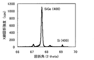
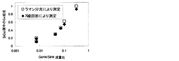
- FIG. 1 is an X-ray diffraction spectrum diagram of a single crystal SiGe thin film according to the present invention. It is a diagram illustrating a SiH 4 flow rate dependency of the single-crystal SiGe film growth rate according to the present invention. Is a diagram illustrating a GeH 4 / SiH 4 flow ratio presence of Ge composition of the single crystal SiGe thin film according to the present invention. It is a Raman spectrum spectrum figure of the single crystal Ge thin film concerning the present invention.
- a semiconductor thin film manufacturing apparatus 1 includes a film forming chamber 2 for forming a thin film, and a preparation chamber 3 that allows the substrate 11 to be taken in and out normally without exposing the film forming chamber 2 to the atmosphere. Become.
- SiH 4 , GeH 4, and F 2 gases are decompressed from the respective gas cylinders 4 to an appropriate pressure by a pressure reducing valve 5 and then supplied into the film forming chamber 2 at a predetermined flow rate by a mass flow controller (also referred to as a mass flow meter) 6. Is done. For safety, these gases may be diluted with an inert gas such as Ar or He.
- the gas outlet 7 may be an independent tube for each raw material gas, or SiH 4 and GeH 4 may be mixed and supplied as a single tube.
- each gas may be discharged from a multi-cylindrical outlet, or SiH 4 , GeH 4, and F 2 are alternately released from adjacent holes from the outlet having a number of holes in a shower head shape. May be.
- a branch that allows the F 2 gas used for film formation to flow separately for etching is provided in the middle of the F 2 gas piping in the middle of the SiH 4 and GeH 4 piping, so that the SiH 4 and GeH after the film formation is completed.
- F 2 instead of 4 fine particles of Si, Ge, and SiGe adhering to the periphery of the gas outlet 7 are removed by etching, and generation of defects due to incorporation of these fine particles into the film can be suppressed.
- SiH 4 and GeH 4 and F 2 flow between the pipes at the same time so that they do not react in the pipes, and between the SiH 4 and GeH 4 supply valves and the F 2 gas branch valve. It is desirable to provide an interlock 8 on the door.
- Ar gas is also supplied from the gas cylinder 9 into the film forming chamber 2 through the pressure reducing valve 5 and the mass flow controller 6 in order to facilitate adjustment of temperature and pressure and improve safety.
- an inert gas such as He may be used instead of Ar.
- the substrate 11 is fixed to the substrate holder 12 and introduced from the preparation chamber 3, evacuated by a turbo molecular pump or the like as the vacuum pump 20, and then transferred to the film formation chamber 2 by opening and closing the gate valve 13.
- the substrate 11 is heated to a predetermined temperature while the temperature is monitored by the substrate heater 14 on the back of the substrate holder 12 and the thermocouple 15 installed in or near the substrate holder 12.
- a reflection high energy electron diffraction (RHEED) apparatus having an RHEED gun and an RHEED screen 16 installed in the film forming chamber 2 may be used.
- the state of the reaction can be confirmed by observing the emission color from the window 18 of the film forming chamber 2.
- the pressure in the film forming chamber 2 is adjusted by a balance with the flow rates of the source gas and the inert gas for dilution by evacuating with a vacuum pump 20 such as a mechanical booster pump or a turbo molecular pump through a pressure adjusting valve 19. To do.
- a material having corrosion resistance against highly reactive F 2 gas As a member inside the film forming chamber 2, it is desirable to use a material having corrosion resistance against highly reactive F 2 gas.
- materials such as the substrate holder 12, the shutter 17, the gas outlet 7, the heat shield 21, the substrate heater 14, and the insulator 22 that become high temperature are relatively resistant to corrosion, such as monel, molybdenum, silicon carbide, and alumina. It is desirable to use etc. Further, it is desirable to use glass coated with a fluoride such as sapphire or magnesium fluoride as the window material. Further, before and after the film formation chamber 2 is opened to the atmosphere, it is desirable to perform sufficient baking in order to remove F 2 and moisture.
- a single-crystal Si substrate on glass (see US Pat. No. 7,176,528, etc.) made by Corning, Inc., in which a thin Si single-crystal film of about 300 nm is bonded to glass, is immersed in a diluted hydrofluoric acid aqueous solution to remove the natural oxide film. After that, it is fixed to the substrate holder 12 and introduced into the preparation chamber 3 of the semiconductor thin film manufacturing apparatus 1 in a short time.
- the substrate holder 12 is transferred to the film formation chamber 2 and heated to about 600 ° C. and left for about 30 minutes to remove the oxide film by the RHEED pattern obtained by the RHEED screen 16. Make sure that it is.
- SiH 4 is diluted with the mass flow controller 6 at 15 sccm, GeH 4 diluted with Ar gas to a volume flow rate ratio of 10% is 11.6 sccm, F 2 is 10 sccm, and Ar for dilution is added. 170 sccm is supplied into the film forming chamber 2, and the pressure is adjusted to about 107 Pa by the pressure adjusting valve 19.
- the shutter 17 is opened and the film formation of SiGe is started. After 30 minutes, the shutter 17 is closed, and supply of each gas and substrate heating are stopped.
- a (100) -oriented SiGe single crystal having a thickness of 3.9 ⁇ m and a Ge composition of 0.44 in molar ratio could be epitaxially grown on a (100) -oriented Si single crystal substrate on glass.
- the substrate temperature In the general thermal CVD method using only SiH 4 and GeH 4 , it is usually necessary to set the substrate temperature to 650 ° C. or more for the film formation of single crystal SiGe, but in the embodiment according to the present invention, glass is mainly used. Even with the substrate 11, a single crystal film could be formed at a low temperature of 550 ° C. without any alteration.
- the substrate 11 is a Si-on-glass substrate with a small amount of Si material used, which is expected to reduce the cost.
- SiGe film to be deposited etc.
- a SiGe single crystal substrate on glass and a more general Si or Ge bulk single crystal substrate may be used.
- the volume flow ratio of GeH 4 and F 2 to SiH 4 is fixed at 12: 1: 12, and the flow rate of Ar to be diluted and the pressure adjustment valve 19 are adjusted, so that the pressure in the film forming chamber 2 is about 107 Pa. While maintaining this, the flow rate of SiH 4 was changed from 9 sccm to 20 sccm, and a SiGe single crystal thin film was grown.
- the Ge composition is approximately 0.5 in molar ratio.
- the growth rate increased as the raw material gas flow rate increased, and a maximum of 13.8 ⁇ m / h (3.8 ⁇ m / sec) and conventional Si 2 H 6 and GeF 4 were used. It was possible to obtain a deposition rate higher than that of the deposition method.
- the volume flow rate of GeH 4 with respect to SiH 4 was formed by changing the ratio from 0.007 to 0.32.
- the substrate temperature was changed from 350 ° C. to 600 ° C. depending on the volume flow rate ratio.
- the Ge composition is 0 in molar ratio according to the volume flow ratio of GeH 4 / SiH 4. It was possible to change within a wide range of 1 to 1.0.
- GeH 4 / SiH 4 volume flow ratio, the substrate temperature, and the pressure for growing the SiGe and Ge single crystal thin films are not limited to the above conditions.
- the volumetric flow ratio of GeH 4 / SiH 4 may be varied in the range of 0.005 to 1.0 depending on the composition of the growing SiGe thin film.
- the substrate temperature is too low, the film becomes amorphous or polycrystallized, and if it is too high, the variation in composition increases due to the diffusion and segregation of Ge atoms, or etching by F 2 becomes significant.
- the temperature is preferably in the range of 350 to 650 ° C.
- the pressure is preferably in the range of 13.3 Pa to 1.33 kPa.
- a Ge bulk single crystal substrate is sequentially immersed in a diluted hydrofluoric acid solution and a hydrogen peroxide solution to form an oxide film on the surface, and then fixed to the substrate holder 12, and in a short time the preparation chamber 3 of the semiconductor thin film manufacturing apparatus 1 To introduce.
- the substrate holder 12 is transferred to the film formation chamber 2 and heated to about 450 ° C. and left for about 30 minutes to remove the oxide film with the RHEED pattern obtained by the RHEED screen 16. Make sure that it is.
- a (100) -oriented Ge single crystal thin film having a thickness of 1.6 ⁇ m could be epitaxially grown on a (100) -oriented Ge bulk single crystal substrate.
- the grown Ge epitaxial film has good crystallinity equivalent to that of the bulk Ge single crystal.
- each film thickness of the Ge epitaxial film 0 .6 ⁇ m and 0.5 ⁇ m, which were smaller than those when SiH 4 and GeH 4 and F 2 were all used simultaneously as in the present invention.
- a p-type Ge single crystal thin film is grown.
- a pn junction having a uniform doping density can be formed, and can be applied to solar cells for the infrared light region.
- a Ge bulk single crystal lattice-matched with a Ge single crystal thin film is used as the substrate 11.
- an Si bulk single crystal substrate or a single crystal thin film of Si or SiGe or Ge on a glass plate is used. It may be a bonded substrate.
- a SiGe polycrystalline substrate on glass in which a SiGe polycrystalline thin film is formed on a glass plate is prepared by a method called an aluminum induced layer exchange growth (AIC) method.
- AIC aluminum induced layer exchange growth
- Al aluminum
- Al aluminum
- the SiGe is polycrystallized by heat treatment at a temperature of 20 ° C. for 20 to 200 hours, and Al deposited on the surface is etched with dilute hydrochloric acid or the like.
- a SiGe polycrystalline substrate on glass having a Ge composition in a molar ratio of 0.5 and a film thickness of 200 nm is prepared by an AIC method, and the surface is immersed in a diluted hydrofluoric acid aqueous solution and a hydrogen peroxide solution sequentially. After the oxide film is formed, the substrate is fixed to the substrate holder 12 and introduced into the preparation chamber 3 of the semiconductor thin film manufacturing apparatus 1 in a short time.
- the substrate holder 12 is transferred to the film formation chamber 2 and heated to about 550 ° C. and left for about 30 minutes to remove the oxide film with the RHEED pattern obtained by the RHEED screen 16. Make sure that it is.
- SiH 4 is supplied at 15 sccm by the mass flow controller 6
- GeH 4 diluted to 10% by volume with Ar gas is supplied at 11.6 sccm
- F 2 is supplied at 10 sccm
- Ar for dilution is supplied at 170 sccm into the film forming chamber 2.
- the pressure is adjusted to a pressure of about 107 Pa by the pressure adjusting valve 19.
- the shutter 17 is opened and the film formation of SiGe is started. After 30 minutes, the shutter 17 is closed, and supply of each gas and substrate heating are stopped.
- a SiGe polycrystalline thin film having a large grain size which was oriented in the same manner as a base substrate having a thickness of 1.5 ⁇ m and a Ge composition of 0.5, could be grown on a SiGe polycrystalline substrate on glass.
- the thermal expansion coefficient of the glass substrate polycrystalline glass coincide with the thermal expansion coefficient of the growing SiGe, it is possible to suppress the occurrence of defects due to thermal strain and warpage of the substrate 11.
- a SiGe polycrystalline substrate on glass having a large grain size and no lattice mismatch was used as the substrate 11, but a polycrystalline Si substrate on glass, a polycrystalline Ge substrate on glass, and an inexpensive glass substrate or metal substrate. May be used.
- the GeH 4 / SiH 4 volume flow ratio, the substrate temperature, and the pressure for growing the SiGe and Ge polycrystalline thin films are not limited to the above conditions.
- the volumetric flow ratio of GeH 4 / SiH 4 may be varied in the range of 0.005 to 1.0 depending on the composition of the growing SiGe thin film.
- the substrate temperature is too low, the film becomes amorphous, and if it is too high, the dispersion of the composition increases due to the diffusion and segregation of Ge atoms, and the etching by F 2 becomes remarkable. It is preferable to be in the range.
- the pressure is too low, the film forming rate is lowered, and if it is too high, it becomes difficult to control. Therefore, the pressure is preferably in the range of 13.3 Pa to 1.33 kPa.
- a Ge polycrystal having a thickness of 1.2 ⁇ m and oriented mainly in the (111) direction could be grown on the glass substrate.
- the present invention when SiH 4 and GeH 4 and F 2 were used at the same time, a Ge deposition rate comparable to 450 ° C. was obtained even at a substrate temperature of 300 ° C. By reducing the substrate temperature, it is possible to further reduce the warpage and defects of the substrate 11 due to thermal strain.
- an inexpensive glass substrate is used as the substrate 11, but a metal substrate may be used, or a substrate in which a polycrystalline thin film of Si, SiGe or Ge is formed on a glass plate or a metal plate. It may be.
- the thermal expansion coefficient of the glass plate or metal plate with the thermal expansion coefficient of the germanium (Ge) or silicon germanium (SiGe) crystal to be grown, the difference in thermal expansion between the grown crystal thin film and glass or metal It is possible to suppress occurrence of defects and warping of the substrate 11.
Landscapes
- Chemical & Material Sciences (AREA)
- Engineering & Computer Science (AREA)
- Crystallography & Structural Chemistry (AREA)
- Materials Engineering (AREA)
- Metallurgy (AREA)
- Organic Chemistry (AREA)
- Chemical Kinetics & Catalysis (AREA)
- General Chemical & Material Sciences (AREA)
- Inorganic Chemistry (AREA)
- Chemical Vapour Deposition (AREA)
- Photovoltaic Devices (AREA)
- Crystals, And After-Treatments Of Crystals (AREA)
Abstract
基板上にガスを供給して半導体薄膜を形成する半導体薄膜結晶の製造方法であって、供給ガスとしてモノシラン(SiH4)、モノゲルマン(GeH4)およびフッ素(F2)並びにそれらを希釈する不活性ガスを用いて、該モノシランに対する該モノゲルマンの体積流量比を0.005以上1以下、フッ素の流量比を体積流量比で0.5~4とし、基板温度を摂氏350度以上650度以下とし、圧力を13.3Pa以上1.33kPa以下とし、基板上にSiGe又はGeの単結晶又は多結晶を成膜することを特徴とする。
Description
本発明は、半導体集積回路あるいは太陽電池等に利用可能な半導体薄膜結晶の製造方法および装置に関する。
既に広く普及している半導体であるシリコン結晶に比べて、シリコンゲルマニウム(SiGe)やゲルマニウム(Ge)の結晶は、バンドギャップが小さいため、特に赤外光領域における高効率の太陽電池や赤外光検出素子としての応用が期待されている。
また、これらの結晶は、シリコン結晶に比べてキャリアの移動度が高いので、超高速の集積回路にも応用が期待される。
シリコンゲルマニウム(SiGe)やゲルマニウム(Ge)の薄膜結晶の製造方法としては、モノシラン(SiH4)、モノゲルマン(GeH4)の熱分解によって基板上に薄膜の堆積を行う熱CVD(化学気相成長)法が一般に知られているが、通常、基板温度は、SiGeの場合で650℃以上、Geの場合でも500℃以上と高く、安価なガラスを主成分とする基板を用いることが困難であり、基板との熱膨張の違いから特に太陽電池に適した厚さ1μm以上の良質の結晶膜を成長させることが困難であった。
一方、SiGeやGeの薄膜を300℃程度の低温で堆積する方法が知られている(例えば、下記特許文献1参照)。この方法は、堆積膜形成用の気体原料物質(直鎖状シラン化合物、直鎖状ゲルマン化合物等)と、該原料物質に酸化作用をする性質を有する気体状ハロゲン酸化剤(フッ素等)とを、反応室空間内に導入して化学的に接触させることにより励起状態の前駆体を含む複数の前駆体を生成し、これらの前駆体のうち少なくとも1つの前駆体を堆積膜構成要素の供給源として成膜空間内にある基体上に堆積膜を形成する堆積膜形成法である。
例えば、直鎖状シラン化合物であるモノシラン(SiH4)を20sccm、直鎖状ゲルマン化合物であるモノゲルマン(GeH4)を5sccm、気体状ハロゲン酸化剤であるF2を5sccm、さらに希釈ガスとしてHeを40sccm、それぞれ流して、内圧を107Paに保つと、基板温度300℃で石英基板上に2時間で厚さ約2μmの水素およびフッ素を含むアモルファスシリコンゲルマニウム(SiGe)膜が堆積できる。本明細書における「sccm」はstandard cc/minの略で標準状態における流量を表す。また、モノゲルマン(GeH4)を20sccm、F2を4sccm、さらにHeを40sccm、それぞれ流して、内圧を107Paに保つと、基板温度300℃で石英基板上に2時間で厚さ約1.5μmの水素およびフッ素を含むアモルファスGe膜が堆積できる。
特許文献1に開示されている技術によれば、300℃程度の低温でSiGeやGeの薄膜を堆積できる。しかしながら、成膜される膜は、アモルファス膜であって、少数キャリア寿命が短く、かつキャリアの移動度が低いため、必ずしも高効率の太陽電池や高速の集積回路などの応用には適さないという問題があった。
また、ジシラン(Si2H6)とフッ化ゲルマニウム(GeF4)の体積流量比をSi2H6:GeF4=20:0.9~40:0.9の範囲で供給し、成膜基板を350~450℃の間で加熱することにより、基板表面にSi組成が80原子%以上の多結晶シリコンゲルマニウム(SiGe)薄膜を成膜することも知られている(例えば、下記特許文献2参照)。
例えば、圧力を133Pa以下でジシラン(Si2H6)流量20sccmに対してフッ化ゲルマニウム(GeF4)の体積流量を0.9~2.7sccmの範囲で変化すると、1.5nm/sec程度の成膜速度でGe組成が20~95原子%のシリコンゲルマニウム(SiGe)多結晶膜が得られている。
さらに類似の方法として、シリコン(Si)に対して200~500℃の範囲において化学的エッチング性を有するフッ化ゲルマニウムガスと、シラン系原料ガスと、該シラン系原料ガスの希釈率を上げるキャリアガスの存在下、前記シラン系原料ガスを加熱された基体により熱的に活性化させることにより、前記フッ化ゲルマニウムガスがSiのネットワーク構造の緩和と結晶化を促進させて前記基体上に多結晶SiGe膜を形成する半導体基材の製造方法であって、前記フッ化ゲルマニウムガスと前記シラン系原料ガスの体積流量比(フッ化ゲルマニウムガス/シラン系原料ガス)が0.07~0.15の範囲内の一定値であり、前記加熱された基体の温度が350~450℃の範囲内の一定温度であり、前記多結晶SiGe膜の形成時の圧力が1.33~2.67kPaの範囲内の一定圧力であり、前記多結晶SiGe膜のSi組成が80原子%以上である半導体基材の製造方法が開示されている(例えば、下記特許文献3参照)。
この方法によれば、例えば、GeF4/Si2H6の体積流量比0.02~0.5で、Ge組成が73~99原子%のSiGe多結晶膜を得ている。成膜速度は最大で2.8nm/sec程度である。
これら特許文献2および3に記載の方法によれば、450℃以下の低温で、比較的に高いキャリア移動度や長い少数キャリア寿命を有するSiGe多結晶薄膜を堆積することができる。
しかしながら、これらの方法は原料ガスとしてGeF4を用いているため、成膜するSiGeの構成要素であるゲルマニウム原料とSi2H6の酸化剤であるフッ素の比率が固定されてしまい、SiGe膜の組成を広範囲に、特に長波長の太陽電池等に有用なGeを多く含む組成で自由に変えることが容易ではなく、また成膜速度にも限界があった。
さらに、ガスの吹出し口や成膜チャンバー内にシリコンやシリコンゲルマニウムの微粒子(ダスト)が発生した場合の除去も、GeF4ではエッチング性が低く困難であった。
本発明は、結晶基板上に、幅広い組成自由度で、かつ高いキャリア移動度や長い少数キャリア寿命を有するSiGeまたはGe結晶薄膜を高い成膜速度で成膜する半導体薄膜結晶の製造方法及び製造装置を提供することにある。
本発明は、上記課題を解決するために、次の特徴を有するものである。
本発明による半導体薄膜結晶の製造方法は、供給ガスとしてモノシラン(SiH4)、モノゲルマン(GeH4)及びフッ素(F2)並びにそれらを希釈する不活性ガスを用い、該モノシランに対する該モノゲルマンの流量比を体積流量比で0.005以上1以下、フッ素の流量比を体積流量比で0.5~4とし、基板温度を摂氏350度以上650度以下とし、圧力を13.3Pa以上1.33kPa以下とし、基板上にSiGe又はGeの単結晶又は多結晶の薄膜を形成することを特徴とする。
上記シリコンゲルマニウム単結晶薄膜又はゲルマニウム単結晶薄膜を形成するための基板は、シリコン、シリコンゲルマニウム又はゲルマニウムのバルク単結晶基板であることが好ましい。
あるいは、ガラス板上にシリコン、シリコンゲルマニウム又はゲルマニウムの単結晶薄膜を接合した基板であることが好ましい。
上記シリコンゲルマニウム多結晶薄膜又はゲルマニウム多結晶薄膜を形成するための基板は、ガラス又は金属であることが好ましい。
あるいは、ガラス板又は金属板上にシリコン、シリコンゲルマニウム又はゲルマニウムの多結晶薄膜を形成した基板であることが好ましい。
また、本発明による半導体薄膜結晶の製造装置は、基板上にガスを供給して半導体薄膜を形成する半導体薄膜結晶の製造装置であって、原料ガスが供給されて基板上に薄膜が成膜される成膜室を備え、前記成膜室内に、前記原料ガスとしてモノシラン、モノゲルマン及びフッ素並びにそれらを希釈する不活性ガスを供給するガス吹き出し口と、前記基板を摂氏350度以上650度以下に加熱する基板ヒーターとを有し、前記原料ガスのモノシランに対するモノゲルマンの流量比を体積流量比で0.005以上1以下、フッ素の流量比を体積流量比で0.5~4に調整して前記成膜室内に前記原料ガスを供給するマスフローコントローラーと、前記成膜室内の圧力を13.3Pa以上1.33kPa以下に調整する真空ポンプとを備え、前記基板上にシリコンゲルマニウム又はゲルマニウムの単結晶又は多結晶の薄膜を形成することを特徴とする半導体薄膜結晶の製造装置である。
この場合、モノシランガス及びモノゲルマンガスの流路にフッ素ガスを供給する分岐を設けたことを特徴とする半導体薄膜結晶の製造装置である。
本発明による半導体薄膜結晶の製造方法においては、供給ガスとしてモノシラン(SiH4)、モノゲルマン(GeH4)及びフッ素(F2)並びにそれらを希釈するアルゴン(Ar)又はヘリウム(He)等の不活性ガスを用い、モノシランの流量に対するモノゲルマンの流量比を体積流量比で0.005~1.0、フッ素の流量比を体積流量比で0.5~4、基板温度を350~650℃、圧力を13.3Pa~1.33kPaの範囲において成膜を行うことにより、結晶基板上に、幅広い組成自由度で、かつ高いキャリア移動度や長い少数キャリア寿命を有するGe組成をモル比で0.1~1.0のSiGeまたはGe結晶薄膜を供給ガス流量に応じた高い成膜速度で成膜することができる。
ここでフッ素は、モノシラン及びモノゲルマンを分解して水素を取り除くために必要である。また、副次的効果として、成膜室のクリーニング作用も行うものである。
ここでフッ素は、モノシラン及びモノゲルマンを分解して水素を取り除くために必要である。また、副次的効果として、成膜室のクリーニング作用も行うものである。
また、SiGe又はGe単結晶薄膜を成長させるための基板としては、シリコン(Si)、ゲルマニウム(Ge)又はシリコンゲルマニウム(SiGe)のバルク単結晶基板を用いると、成長したエピタキシャル膜は、バルク単結晶と同等の良好な結晶性を有するものができる。あるいは、ガラス板上にSi、Ge又はSiGeの単結晶薄膜を接合した基板を用いることで、安価なガラスを主体とすることができる。
また、SiGeまたはGe多結晶薄膜を成長させるための基板としては、ガラス又は金属を用いるとよく、特にガラス基板を用いるとコストを低くできる。あるいは、ガラス板又は金属板上に結晶粒径が大きく配向性の高いSi、Ge又はSiGeの多結晶薄膜を形成した基板を用いることにより、下地の結晶粒径や配向性を反映した良質のSiGeまたはGeの多結晶薄膜を厚く成長させることができる。
本発明による半導体薄膜結晶の製造装置は、供給ガスとしてモノシラン(SiH4)、モノゲルマン(GeH4)及びフッ素(F2)並びに必要に応じてそれらを希釈するアルゴン(Ar)又はヘリウム(He)等の不活性ガスを用い、SiH4流量に対するGeH4の流量比を体積流量比で0.005~1.0、F2の流量比を体積流量比で0.5~4、基板温度を350~650℃、圧力を13.3Pa~1.33kPaの範囲とすることにより、幅広い組成自由度で、かつ高いキャリア移動度や長い少数キャリア寿命を有するGe組成をモル比で0.1~1.0のSiGeまたはGe結晶薄膜を供給ガス流量に応じて高い成膜速度で成膜することができる。
また、前記半導体薄膜結晶の製造装置に、モノシラン(SiH4)及びモノゲルマン(GeH4)ガスの流路にフッ素(F2)ガスも供給できる分岐を設けたことにより、成膜終了後、SiH4およびGeH4ガスの流路にF2ガスを流すことにより、ガスの吹出し口及び基板ホルダー周辺に付着したSi、Ge及びSiGeの微粒子をエッチングにより除去し、成膜時のこれら微粒子の薄膜中への取り込みを抑止することができる。
本発明の上記及び他の特徴及び利点は、適宜添付の図面を参照して、下記の記載からより明らかになるであろう。
本発明による半導体薄膜製造装置の概要を図1に示す。
本発明による半導体薄膜製造装置1は、薄膜の成膜を行う成膜室2と、通常は成膜室2を大気にさらすことなく外部との基板11の出し入れを行うことができる準備室3からなる。
本発明による半導体薄膜製造装置1は、薄膜の成膜を行う成膜室2と、通常は成膜室2を大気にさらすことなく外部との基板11の出し入れを行うことができる準備室3からなる。
SiH4、GeH4およびF2ガスは、それぞれのガスボンベ4から減圧弁5で適当な圧力まで減圧した後、マスフローコントローラー(マスフローメーターともいう。)6により所定の流量で成膜室2内に供給される。これらのガスは安全のため、ArやHeなどの不活性ガスで希釈したものを用いてもよい。
これらの供給ガスは、成膜室2内で基板11表面に対向したガス吹出し口7から放出される。ガス吹出し口7は、図1に示すように、それぞれの原料ガスごとに独立した管でもよいし、SiH4およびGeH4を混合して一つの管で供給してもよい。また、多重円筒型の吹出し口からそれぞれのガスを放出してもよいし、シャワーヘッド状に多数の穴のある吹出し口からSiH4、GeH4およびF2を交互に隣り合った穴から放出してもよい。
ここで、F2ガスの配管の途中に、SiH4およびGeH4の配管の途中へ成膜に用いるF2ガスを別途エッチング用としても流せる分岐を設けることにより、成膜終了後SiH4およびGeH4の代わりにF2を流して、ガス吹出し口7の周辺に付着したSi、GeおよびSiGeの微粒子をエッチングにより除去し、これら微粒子の膜中への取込みによる欠陥の発生を抑止できる。
その際、安全のため、SiH4およびGeH4とF2とが同時に配管に流れて配管内で反応を起こさないよう、SiH4およびGeH4の供給バルブとF2ガスの分岐部のバルブの間にインターロック8を設けることが望ましい。
一方、温度や圧力の調整を容易にし、安全性を向上するため、Arガスも同様にガスボンベ9から減圧弁5、マスフローコントローラー6を介して成膜室2内に供給する。ここで、Arに代えてHeなどの不活性ガスを用いてもよい。
基板11は、基板ホルダー12に固定して準備室3から導入し、真空ポンプ20としてのターボ分子ポンプ等で真空引きした後、ゲートバルブ13を開閉して成膜室2内に移送する。
成膜室2内においては、基板ホルダー12背面にある基板ヒーター14で、基板ホルダー12またはその近傍に設置した熱電対15で温度をモニタしながら、所定の温度まで基板11の加熱を行う。
基板11表面の酸化膜が加熱により除去されたかどうかを確認するため、成膜室2に設置したRHEED銃とRHEEDスクリーン16を有する反射高エネルギー電子線回折(RHEED)装置を用いてもよい。
基板11とガス吹出し口7の間にシャッター17を設けることで、SiH4およびGeH4とF2ガスを流し始めてガス間の反応が安定してから、シャッター17を開けて成膜を開始することができる。
反応の様子は、成膜室2の窓18から発光色を観察することにより、確認できる。成膜室2内の圧力は、圧力調整弁19を介してメカニカルブースターポンプやターボ分子ポンプ等の真空ポンプ20で真空引きすることにより、原料ガスおよび希釈用不活性ガスの流量とのバランスで調整する。
成膜室2内部の部材は、反応性の高いF2ガスに対して耐腐食性を有する材料を用いることが望ましい。特に、高温となる基板ホルダー12、シャッター17、ガス吹出し口7、熱シールド21、基板ヒーター14、絶縁体22などの材料は、比較的に耐腐食性のある、モネル、モリブデン、炭化珪素、アルミナなどを用いることが望ましい。また、窓材には、サファイヤやフッ化マグネシウムなどのフッ化物をコートしたガラスを用いることが望ましい。さらに、成膜室2を大気開放する前後は、F2や水分を除去するため、十分にベーキングを行うことが望ましい。
<SiGe単結晶薄膜の製造>
米国コーニング社製の、300nm程度の薄いSi単結晶膜をガラスに接合したガラス上Si単結晶基板(米国特許第7176528号等参照)を、希釈したフッ酸水溶液に浸漬して自然酸化膜を除去した後、基板ホルダー12に固定し、短時間で前記半導体薄膜製造装置1の準備室3に導入する。
米国コーニング社製の、300nm程度の薄いSi単結晶膜をガラスに接合したガラス上Si単結晶基板(米国特許第7176528号等参照)を、希釈したフッ酸水溶液に浸漬して自然酸化膜を除去した後、基板ホルダー12に固定し、短時間で前記半導体薄膜製造装置1の準備室3に導入する。
準備室3を十分に真空引きした後、基板ホルダー12を成膜室2に移送して約600℃まで加熱し、30分程度放置して、RHEEDスクリーン16で得られるRHEEDパターンで酸化膜が除去されていることを確認する。
その後、基板温度を550℃まで下げ、安定したら、マスフローコントローラー6でSiH4を15sccm、Arガスで体積流量比10%に希釈したGeH4を11.6sccm、F2を10sccm、希釈用のArを170sccm、それぞれ成膜室2内に供給し、圧力調整弁19で約107Paの圧力に調整する。
青白い発光反応が安定したら、シャッター17を開け、SiGeの成膜を開始する。30分後にシャッター17を閉め、各ガスの供給と基板加熱を停止する。
このような方法で、ガラス上(100)方位Si単結晶基板の上に厚さ3.9μm、Ge組成をモル比で0.44の(100)方位SiGe単結晶をエピタキシャル成長させることができた。
図2のX線回折測定結果に示すように、成膜したSiGeは若干のGe組成の分布はあるものの、良好な結晶性を有することが確認された。
一般的なSiH4とGeH4のみを用いた熱CVD法では、通常単結晶SiGeの成膜には基板温度を650℃以上にする必要があるが、本発明による実施例ではガラスを主とする基板11でも全く変質のない550℃という低温で、単結晶の成膜を実現できた。
ここで、基板11にはSi材料資源の使用量が少なく低コスト化が期待されるガラス上Si単結晶基板を用いたが、堆積するSiGe膜の組成等によって他にガラス上Ge単結晶基板やガラス上SiGe単結晶基板、そしてより一般的なSiやGeのバルク単結晶基板を用いてもよい。
また、ガラス上単結晶基板においてガラスの熱膨張係数を成長するSiGeの熱膨張係数に一致させることで、熱歪による欠陥や基板11のそりの発生を抑止することができる。
次に、SiH4に対するGeH4およびF2の体積流量比を12:1:12に固定し、希釈するArの流量と圧力調整弁19を調整して成膜室2内の圧力を約107Paに保ちながら、SiH4の流量を9sccmから20sccmまで変化させてSiGe単結晶薄膜の成長を行った。Ge組成はモル比でほぼ0.5である。
その結果、図3に示すように、成長速度は原料ガス流量が多いほど増大し、最大で13.8μm/h(3.8μm/sec)と従来のSi2H6とGeF4とを用いた成膜法よりも大きな成膜速度を得ることができた。
次に、SiH4の流量を15sccm、F2の流量を20sccmに固定し、希釈するArの流量と圧力調整弁19を調整して圧力を約107Paに保ちながら、SiH4に対するGeH4の体積流量比を0.007から0.32まで変化させてSiGe単結晶の成膜を行った。ここで、基板温度は体積流量比によって350℃から600℃まで変化させた。
成膜したSiGe中のGe組成をラマン分光法およびX線回折法による測定から推定した結果、図4に示すように、GeH4/SiH4の体積流量比に応じてGe組成をモル比で0.1~1.0の広い範囲で変えることができた。
なお、SiGeおよびGe単結晶薄膜の成長を行うGeH4/SiH4の体積流量比、基板温度および圧力は上記の条件に限られるものではない。GeH4/SiH4の体積流量比は成長するSiGe薄膜の組成に応じて0.005~1.0の範囲で変えてもよい。
また、基板温度は、温度が低すぎると膜がアモルファス化または多結晶化し、高すぎるとGe原子の拡散・偏析によって組成のバラツキが大きくなったり、F2によるエッチングが顕著になったりするので、350~650℃の範囲とするのが好ましい。また、圧力は低すぎると成膜速度が低下し、高すぎると制御が困難になるので、13.3Pa~1.33kPaの範囲とすることが好ましい。
<Ge単結晶薄膜の製造>
Geバルク単結晶基板を希釈したフッ酸水溶液、過酸化水素溶液に順次浸漬して表面に酸化膜を形成した後、基板ホルダー12に固定し、短時間で前記半導体薄膜製造装置1の準備室3に導入する。
Geバルク単結晶基板を希釈したフッ酸水溶液、過酸化水素溶液に順次浸漬して表面に酸化膜を形成した後、基板ホルダー12に固定し、短時間で前記半導体薄膜製造装置1の準備室3に導入する。
準備室3を十分に真空引きした後、基板ホルダー12を成膜室2に移送して約450℃まで加熱し、30分程度放置して、RHEEDスクリーン16で得られるRHEEDパターンで酸化膜が除去されていることを確認する。
その後、マスフローコントローラー6でSiH4を5sccm、Arガスで体積流量比10%に希釈したGeH4を50sccm、F2を5sccm、希釈用のArを100sccm、それぞれ成膜室2内に供給し、圧力調整弁19で約107Paの圧力に調整する。青白い発光反応が安定したら、シャッター17を開け、Geの成膜を開始する。20分後にシャッター17を閉め、各ガスの供給と基板加熱を停止する。
このような方法で、(100)方位Geバルク単結晶基板の上に厚さ1.6μmの(100)方位Ge単結晶薄膜をエピタキシャル成長させることができた。図5のラマン分光測定結果に示すように、成長したGeエピタキシャル膜は、バルクGe単結晶と同等の良好な結晶性を有することが確認された。
次に他を同じ条件で、SiH4の体積流量をゼロにした場合とSiH4およびF2の体積流量をゼロにした場合について成膜を行ったところ、Geエピタキシャル膜の膜厚はそれぞれ、0.6μmおよび0.5μmとなり、本発明のように、SiH4およびGeH4とF2を全て同時に用いた場合に比べて小さかった。
これは、単独のGeH4熱分解反応やGeH4とF2のみの反応による分解反応に対し、SiH4を加えることでGeH4の分解がより加速され、Ge成長速度の向上に寄与しているものと考えられる。
また、本発明により、SiH4およびGeH4とF2を同時に用いた場合には、基板温度300℃でも450℃と同程度のGe成長速度が得られた。
本実施例において、例えばn型のGeバルク単結晶基板を用い、エピタキシャル成長時にAr等で希釈したジボラン(B2H6)ガスを同時に供給することでp型のGe単結晶薄膜の成長を行えば、ドーピング密度の均質なpn接合が形成でき、赤外光領域用の太陽電池等に応用することができる。
なお、本実施例において、基板11にはGe単結晶薄膜と格子整合するGeバルク単結晶を用いたが、安価なSiバルク単結晶基板やガラス板上にSi又はSiGe又はGeの単結晶薄膜を接合した基板であってもよい。
なお、本実施例において、基板11にはGe単結晶薄膜と格子整合するGeバルク単結晶を用いたが、安価なSiバルク単結晶基板やガラス板上にSi又はSiGe又はGeの単結晶薄膜を接合した基板であってもよい。
<SiGe多結晶薄膜の製造>
ガラス板上にSiGeの多結晶薄膜を形成したガラス上SiGe多結晶基板を、アルミニウム誘起層交換成長(AIC)法と呼ばれる方法で用意する。これはガラス板にアルミニウム(Al)膜をスパッタ等で堆積し、表面を自然酸化した後、所定の組成のアモルファスSiGeをスパッタ等でさらに堆積した後、窒素等の不活性ガス中で420~450℃の温度で20~200時間熱処理してSiGeを多結晶化し、希塩酸などで表面に析出したAlをエッチングして作製するものである。
ガラス板上にSiGeの多結晶薄膜を形成したガラス上SiGe多結晶基板を、アルミニウム誘起層交換成長(AIC)法と呼ばれる方法で用意する。これはガラス板にアルミニウム(Al)膜をスパッタ等で堆積し、表面を自然酸化した後、所定の組成のアモルファスSiGeをスパッタ等でさらに堆積した後、窒素等の不活性ガス中で420~450℃の温度で20~200時間熱処理してSiGeを多結晶化し、希塩酸などで表面に析出したAlをエッチングして作製するものである。
本実施例では、AIC法でGe組成がモル比で0.5、膜厚200nmのガラス上SiGe多結晶基板を作製し、それを希釈したフッ酸水溶液、過酸化水素溶液に順次浸漬して表面に酸化膜を形成した後、基板ホルダー12に固定し、短時間で前記半導体薄膜製造装置1の準備室3に導入する。
準備室3を十分に真空引きした後、基板ホルダー12を成膜室2に移送して約550℃まで加熱し、30分程度放置して、RHEEDスクリーン16で得られるRHEEDパターンで酸化膜が除去されていることを確認する。
その後、マスフローコントローラー6でSiH4を15sccm、Arガスで体積流量比10%に希釈したGeH4を11.6sccm、F2を10sccm、希釈用のArを170sccm、それぞれ成膜室2内に供給し、圧力調整弁19で約107Paの圧力に調整する。
青白い発光反応が安定したら、シャッター17を開け、SiGeの成膜を開始する。30分後にシャッター17を閉め、各ガスの供給と基板加熱を停止する。
このような方法で、ガラス上SiGe多結晶基板の上に厚さ1.5μm、Ge組成0.5の下地基板と同様に配向した粒径の大きなSiGe多結晶薄膜を成長させることができた。ここで、ガラス上多結晶基板のガラスの熱膨張係数を成長するSiGeの熱膨張係数に一致させることで、熱歪による欠陥や基板11のそりの発生を抑止することができる。
ここで、基板11には粒径が大きく格子不整合のないガラス上SiGe多結晶基板を用いたが、ガラス上多結晶Si基板やガラス上多結晶Ge基板、さらには安価なガラス基板や金属基板を用いてもよい。
なお、SiGeおよびGe多結晶薄膜の成長を行うGeH4/SiH4の体積流量比、基板温度および圧力は上記の条件に限られるものではない。GeH4/SiH4の体積流量比は成長するSiGe薄膜の組成に応じて0.005~1.0の範囲で変えてもよい。また、基板温度は、温度が低すぎると膜がアモルファス化し、高すぎるとGe原子の拡散・偏析によって組成のバラツキが大きくなったり、F2によるエッチングが顕著になったりするので、350~650℃の範囲とするのが好ましい。また、圧力は低すぎると成膜速度が低下し、高すぎると制御が困難になるので、13.3Pa~1.33kPaの範囲とすることが好ましい。
<Ge多結晶薄膜の製造>
無アルカリ系のガラス基板を有機洗浄した後、基板ホルダー12に固定し、前記半導体薄膜製造装置1の準備室3に導入する。準備室3を十分に真空引きした後、基板ホルダー12を成膜室2に移送して約450℃まで加熱し、20分程度放置した後、マスフローメーター6でSiH4を5sccm、Arガスで体積流量比10%に希釈したGeH4を50sccm、F2を5sccm、希釈用のArを100sccm、それぞれ成膜室2内に供給し、圧力調整弁19で約107Paの圧力に調整する。青白い発光反応が安定したら、シャッター17を開け、Geの成膜を開始する。30分後にシャッター17を閉め、各ガスの供給と基板加熱を停止する。
無アルカリ系のガラス基板を有機洗浄した後、基板ホルダー12に固定し、前記半導体薄膜製造装置1の準備室3に導入する。準備室3を十分に真空引きした後、基板ホルダー12を成膜室2に移送して約450℃まで加熱し、20分程度放置した後、マスフローメーター6でSiH4を5sccm、Arガスで体積流量比10%に希釈したGeH4を50sccm、F2を5sccm、希釈用のArを100sccm、それぞれ成膜室2内に供給し、圧力調整弁19で約107Paの圧力に調整する。青白い発光反応が安定したら、シャッター17を開け、Geの成膜を開始する。30分後にシャッター17を閉め、各ガスの供給と基板加熱を停止する。
このような方法で、ガラス基板の上に厚さ1.2μmの主として(111)方位に配向したGe多結晶を成長させることができた。
次に他を同じ条件で、SiH4の流量をゼロにした場合とSiH4およびF2の流量をゼロにした場合について成膜を行ったところ、Ge多結晶膜の膜厚はそれぞれ、0.3μmおよび0.2μmとなり、本発明のように、SiH4およびGeH4とF2を全て同時に用いた場合に比べて小さかった。これは、単独のGeH4熱分解反応やGeH4とF2の反応による分解反応に対し、SiH4を加えることでGeH4の分解がより加速され、Ge膜堆積速度の向上に寄与しているものと考えられる。
本発明により、SiH4およびGeH4とF2を同時に用いた場合には、基板温度300℃でも450℃と同程度のGe堆積速度が得られた。基板温度を下げることで、熱歪による基板11のそりや欠陥の発生をより低減することができる。
なお、本実施例において、基板11には安価なガラス基板を用いたが、金属基板を用いてもよいし、あるいはSi、SiGe又はGeの多結晶薄膜をガラス板又は金属板上に形成した基板であってもよい。
また、前記ガラス板又は金属板の熱膨張係数を成長するゲルマニウム(Ge)又はシリコンゲルマニウム(SiGe)結晶の熱膨張係数と整合させることにより、成長結晶薄膜とガラス又は金属との熱膨張の違いに起因する欠陥の発生や基板11のそりを抑制することができる。
なお、本実施例において、基板11には安価なガラス基板を用いたが、金属基板を用いてもよいし、あるいはSi、SiGe又はGeの多結晶薄膜をガラス板又は金属板上に形成した基板であってもよい。
また、前記ガラス板又は金属板の熱膨張係数を成長するゲルマニウム(Ge)又はシリコンゲルマニウム(SiGe)結晶の熱膨張係数と整合させることにより、成長結晶薄膜とガラス又は金属との熱膨張の違いに起因する欠陥の発生や基板11のそりを抑制することができる。
本発明をその実施例とともに説明したが、我々は特に指定しない限り我々の発明を説明のどの細部においても限定しようとするものではなく、添付の請求の範囲に示した発明の精神と範囲に反することなく幅広く解釈されるべきであると考える。
本願は、2011年5月24日に日本国で特許出願された特願2011-115630に基づく優先権を主張するものであり、これはここに参照してその内容を本明細書の記載の一部として取り込む。
1、半導体薄膜製造装置
2、成膜室
3、準備室
4、ガスボンベ
5、減圧弁
6、マスフローコントローラー
7、ガス吹出し口
8、インターロック
9、Arボンベ
11、基板
12、基板ホルダー
13、ゲートバルブ
14、基板ヒーター
15、熱電対
16、RHEEDスクリーン
17、シャッター
18、窓
19、圧力調整弁
20、真空ポンプ
21、熱シールド
22、絶縁体
2、成膜室
3、準備室
4、ガスボンベ
5、減圧弁
6、マスフローコントローラー
7、ガス吹出し口
8、インターロック
9、Arボンベ
11、基板
12、基板ホルダー
13、ゲートバルブ
14、基板ヒーター
15、熱電対
16、RHEEDスクリーン
17、シャッター
18、窓
19、圧力調整弁
20、真空ポンプ
21、熱シールド
22、絶縁体
Claims (7)
- 基板上にガスを供給して半導体薄膜を形成する半導体薄膜結晶の製造方法であって、供給ガスとしてモノシラン、モノゲルマン及びフッ素並びにそれらを希釈する不活性ガスを用い、該モノシランに対する該モノゲルマンの流量比を体積流量比で0.005以上1以下、フッ素の流量比を体積流量比で0.5~4とし、基板温度を摂氏350度以上650度以下とし、圧力を13.3Pa以上1.33kPa以下とし、基板上にシリコンゲルマニウム又はゲルマニウムの単結晶又は多結晶の薄膜を形成することを特徴とする半導体薄膜結晶の製造方法。
- 上記シリコンゲルマニウム単結晶薄膜又はゲルマニウム単結晶薄膜を形成するための基板は、シリコン、シリコンゲルマニウム又はゲルマニウムのバルク単結晶基板であることを特徴とする請求項1に記載の半導体薄膜結晶の製造方法。
- 上記シリコンゲルマニウム単結晶薄膜又はゲルマニウム単結晶薄膜を形成するための基板は、ガラス板上にシリコン、シリコンゲルマニウム又はゲルマニウムの単結晶薄膜を接合した基板であることを特徴とする請求項1に記載の半導体薄膜結晶の製造方法。
- 上記シリコンゲルマニウム多結晶薄膜又はゲルマニウム多結晶薄膜を形成するための基板は、ガラス又は金属であることを特徴とする請求項1に記載の半導体薄膜結晶の製造方法。
- 上記シリコンゲルマニウム多結晶薄膜又はゲルマニウム多結晶薄膜を形成するための基板は、ガラス板又は金属板上にシリコン、シリコンゲルマニウム若しくはゲルマニウムの多結晶薄膜を形成した基板であることを特徴とする請求項1に記載の半導体薄膜結晶の製造方法。
- 基板上にガスを供給して半導体薄膜を形成する半導体薄膜結晶の製造装置であって、原料ガスが供給されて基板上に薄膜が成膜される成膜室を備え、前記成膜室内に、前記原料ガスとしてモノシラン、モノゲルマン及びフッ素並びにそれらを希釈する不活性ガスを供給するガス吹き出し口と、前記基板を摂氏350度以上650度以下に加熱する基板ヒーターとを有し、前記原料ガスのモノシランに対するモノゲルマンの流量比を体積流量比で0.005以上1以下、フッ素の流量比を体積流量比で0.5~4に調整して前記成膜室内に前記原料ガスを供給するマスフローコントローラーと、前記成膜室内の圧力を13.3Pa以上1.33kPa以下に調整する真空ポンプとを備え、前記基板上にシリコンゲルマニウム又はゲルマニウムの単結晶又は多結晶の薄膜を形成することを特徴とする半導体薄膜結晶の製造装置。
- モノシランガス及びモノゲルマンガスの流路にフッ素ガスを供給する分岐を設けたことを特徴とする請求項6に記載の半導体薄膜結晶の製造装置。
Applications Claiming Priority (2)
| Application Number | Priority Date | Filing Date | Title |
|---|---|---|---|
| JP2011115630A JP2014144875A (ja) | 2011-05-24 | 2011-05-24 | 半導体薄膜結晶の製造方法および装置 |
| JP2011-115630 | 2011-05-24 |
Publications (1)
| Publication Number | Publication Date |
|---|---|
| WO2012161265A1 true WO2012161265A1 (ja) | 2012-11-29 |
Family
ID=47217337
Family Applications (1)
| Application Number | Title | Priority Date | Filing Date |
|---|---|---|---|
| PCT/JP2012/063352 Ceased WO2012161265A1 (ja) | 2011-05-24 | 2012-05-24 | 半導体薄膜結晶の製造方法および装置 |
Country Status (2)
| Country | Link |
|---|---|
| JP (1) | JP2014144875A (ja) |
| WO (1) | WO2012161265A1 (ja) |
Families Citing this family (1)
| Publication number | Priority date | Publication date | Assignee | Title |
|---|---|---|---|---|
| JP7232499B2 (ja) * | 2018-09-03 | 2023-03-03 | 国立大学法人 筑波大学 | 半導体装置とその製造方法および光電変換装置 |
Citations (3)
| Publication number | Priority date | Publication date | Assignee | Title |
|---|---|---|---|---|
| JPS62151573A (ja) * | 1985-12-25 | 1987-07-06 | Canon Inc | 堆積膜形成法 |
| JPS62158875A (ja) * | 1985-12-28 | 1987-07-14 | Canon Inc | 堆積膜形成法 |
| JPH08203847A (ja) * | 1995-01-25 | 1996-08-09 | Nec Corp | 半導体装置の製造方法 |
-
2011
- 2011-05-24 JP JP2011115630A patent/JP2014144875A/ja not_active Withdrawn
-
2012
- 2012-05-24 WO PCT/JP2012/063352 patent/WO2012161265A1/ja not_active Ceased
Patent Citations (3)
| Publication number | Priority date | Publication date | Assignee | Title |
|---|---|---|---|---|
| JPS62151573A (ja) * | 1985-12-25 | 1987-07-06 | Canon Inc | 堆積膜形成法 |
| JPS62158875A (ja) * | 1985-12-28 | 1987-07-14 | Canon Inc | 堆積膜形成法 |
| JPH08203847A (ja) * | 1995-01-25 | 1996-08-09 | Nec Corp | 半導体装置の製造方法 |
Also Published As
| Publication number | Publication date |
|---|---|
| JP2014144875A (ja) | 2014-08-14 |
Similar Documents
| Publication | Publication Date | Title |
|---|---|---|
| TWI751115B (zh) | 形成矽鍺錫膜的方法 | |
| CN113235047B (zh) | 一种AlN薄膜的制备方法 | |
| US9218962B2 (en) | Low temperature epitaxy of a semiconductor alloy including silicon and germanium employing a high order silane precursor | |
| US8642454B2 (en) | Low temperature selective epitaxy of silicon germanium alloys employing cyclic deposit and etch | |
| JP2018522412A (ja) | 単結晶シリコン上でのエピタキシャル3C−SiCの成長 | |
| CN108166056A (zh) | 一种能够有效降低碳化硅外延表面缺陷的生长方法 | |
| US20170051400A1 (en) | Method for manufacturing a doped metal chalcogenide thin film, and same thin film | |
| TWI893031B (zh) | 磊晶晶圓之製造方法 | |
| WO2008096884A1 (ja) | n型導電性窒化アルミニウム半導体結晶及びその製造方法 | |
| CN107419333B (zh) | 一种高迁移率铌掺杂氧化锡单晶薄膜的制备方法 | |
| JP5910430B2 (ja) | エピタキシャル炭化珪素ウエハの製造方法 | |
| CN117672815A (zh) | 一种SiC外延片及其制备方法 | |
| JP7259906B2 (ja) | ヘテロエピタキシャルウェーハの製造方法 | |
| CN108511322B (zh) | 一种在二维石墨衬底上制备GaN薄膜的方法 | |
| CN113053732A (zh) | 一种以金刚石为衬底生长的高质量六方氮化硼薄膜及其制备方法 | |
| CN112136203B (zh) | SiC外延基板的制造方法 | |
| JP2024500584A (ja) | 高品質なヘテロエピタキシャル単斜晶ガリウム酸化物結晶の成長方法 | |
| Teplin et al. | Mechanisms controlling the phase and dislocation density in epitaxial silicon films grown from silane below 800 C | |
| JP2014144875A (ja) | 半導体薄膜結晶の製造方法および装置 | |
| JP2004363510A (ja) | 半導体基板の製造方法 | |
| JP7567210B2 (ja) | 炭化珪素単結晶基板の製造方法 | |
| Shin et al. | Effects of different annealing atmospheres on the surface and microstructural properties of ZnO thin films grown on p-Si (1 0 0) substrates | |
| JP5032522B2 (ja) | 化合物半導体エピタキシャルウェハおよびその製造方法 | |
| CN117328142A (zh) | 一种六方氮化硼衬底上范德华外延β相氧化镓薄膜的方法 | |
| TW202344699A (zh) | 單晶半導體膜之製造方法、單晶半導體膜之積層膜之製造方法以及半導體元件 |
Legal Events
| Date | Code | Title | Description |
|---|---|---|---|
| 121 | Ep: the epo has been informed by wipo that ep was designated in this application |
Ref document number: 12790004 Country of ref document: EP Kind code of ref document: A1 |
|
| NENP | Non-entry into the national phase |
Ref country code: DE |
|
| 122 | Ep: pct application non-entry in european phase |
Ref document number: 12790004 Country of ref document: EP Kind code of ref document: A1 |
|
| NENP | Non-entry into the national phase |
Ref country code: JP |