WO2012161014A1 - 照明装置、それを備えた表示装置、およびそれを備えたテレビ受信装置 - Google Patents
照明装置、それを備えた表示装置、およびそれを備えたテレビ受信装置 Download PDFInfo
- Publication number
- WO2012161014A1 WO2012161014A1 PCT/JP2012/062287 JP2012062287W WO2012161014A1 WO 2012161014 A1 WO2012161014 A1 WO 2012161014A1 JP 2012062287 W JP2012062287 W JP 2012062287W WO 2012161014 A1 WO2012161014 A1 WO 2012161014A1
- Authority
- WO
- WIPO (PCT)
- Prior art keywords
- light
- light source
- light guide
- display device
- lighting device
- Prior art date
- Legal status (The legal status is an assumption and is not a legal conclusion. Google has not performed a legal analysis and makes no representation as to the accuracy of the status listed.)
- Ceased
Links
Images

Classifications
-
- H—ELECTRICITY
- H04—ELECTRIC COMMUNICATION TECHNIQUE
- H04N—PICTORIAL COMMUNICATION, e.g. TELEVISION
- H04N5/00—Details of television systems
- H04N5/64—Constructional details of receivers, e.g. cabinets or dust covers
- H04N5/65—Holding-devices for protective discs or for picture masks
-
- G—PHYSICS
- G02—OPTICS
- G02F—OPTICAL DEVICES OR ARRANGEMENTS FOR THE CONTROL OF LIGHT BY MODIFICATION OF THE OPTICAL PROPERTIES OF THE MEDIA OF THE ELEMENTS INVOLVED THEREIN; NON-LINEAR OPTICS; FREQUENCY-CHANGING OF LIGHT; OPTICAL LOGIC ELEMENTS; OPTICAL ANALOGUE/DIGITAL CONVERTERS
- G02F1/00—Devices or arrangements for the control of the intensity, colour, phase, polarisation or direction of light arriving from an independent light source, e.g. switching, gating or modulating; Non-linear optics
- G02F1/01—Devices or arrangements for the control of the intensity, colour, phase, polarisation or direction of light arriving from an independent light source, e.g. switching, gating or modulating; Non-linear optics for the control of the intensity, phase, polarisation or colour
- G02F1/13—Devices or arrangements for the control of the intensity, colour, phase, polarisation or direction of light arriving from an independent light source, e.g. switching, gating or modulating; Non-linear optics for the control of the intensity, phase, polarisation or colour based on liquid crystals, e.g. single liquid crystal display cells
- G02F1/133—Constructional arrangements; Operation of liquid crystal cells; Circuit arrangements
- G02F1/1333—Constructional arrangements; Manufacturing methods
- G02F1/1335—Structural association of cells with optical devices, e.g. polarisers or reflectors
- G02F1/1336—Illuminating devices
- G02F1/133602—Direct backlight
- G02F1/133603—Direct backlight with LEDs
-
- G—PHYSICS
- G02—OPTICS
- G02F—OPTICAL DEVICES OR ARRANGEMENTS FOR THE CONTROL OF LIGHT BY MODIFICATION OF THE OPTICAL PROPERTIES OF THE MEDIA OF THE ELEMENTS INVOLVED THEREIN; NON-LINEAR OPTICS; FREQUENCY-CHANGING OF LIGHT; OPTICAL LOGIC ELEMENTS; OPTICAL ANALOGUE/DIGITAL CONVERTERS
- G02F1/00—Devices or arrangements for the control of the intensity, colour, phase, polarisation or direction of light arriving from an independent light source, e.g. switching, gating or modulating; Non-linear optics
- G02F1/01—Devices or arrangements for the control of the intensity, colour, phase, polarisation or direction of light arriving from an independent light source, e.g. switching, gating or modulating; Non-linear optics for the control of the intensity, phase, polarisation or colour
- G02F1/13—Devices or arrangements for the control of the intensity, colour, phase, polarisation or direction of light arriving from an independent light source, e.g. switching, gating or modulating; Non-linear optics for the control of the intensity, phase, polarisation or colour based on liquid crystals, e.g. single liquid crystal display cells
- G02F1/133—Constructional arrangements; Operation of liquid crystal cells; Circuit arrangements
- G02F1/1333—Constructional arrangements; Manufacturing methods
- G02F1/1335—Structural association of cells with optical devices, e.g. polarisers or reflectors
- G02F1/1336—Illuminating devices
- G02F1/133615—Edge-illuminating devices, i.e. illuminating from the side
-
- G—PHYSICS
- G02—OPTICS
- G02F—OPTICAL DEVICES OR ARRANGEMENTS FOR THE CONTROL OF LIGHT BY MODIFICATION OF THE OPTICAL PROPERTIES OF THE MEDIA OF THE ELEMENTS INVOLVED THEREIN; NON-LINEAR OPTICS; FREQUENCY-CHANGING OF LIGHT; OPTICAL LOGIC ELEMENTS; OPTICAL ANALOGUE/DIGITAL CONVERTERS
- G02F1/00—Devices or arrangements for the control of the intensity, colour, phase, polarisation or direction of light arriving from an independent light source, e.g. switching, gating or modulating; Non-linear optics
- G02F1/01—Devices or arrangements for the control of the intensity, colour, phase, polarisation or direction of light arriving from an independent light source, e.g. switching, gating or modulating; Non-linear optics for the control of the intensity, phase, polarisation or colour
- G02F1/13—Devices or arrangements for the control of the intensity, colour, phase, polarisation or direction of light arriving from an independent light source, e.g. switching, gating or modulating; Non-linear optics for the control of the intensity, phase, polarisation or colour based on liquid crystals, e.g. single liquid crystal display cells
- G02F1/133—Constructional arrangements; Operation of liquid crystal cells; Circuit arrangements
- G02F1/1333—Constructional arrangements; Manufacturing methods
- G02F1/1335—Structural association of cells with optical devices, e.g. polarisers or reflectors
- G02F1/1336—Illuminating devices
- G02F1/133602—Direct backlight
- G02F1/133606—Direct backlight including a specially adapted diffusing, scattering or light controlling members
- G02F1/133607—Direct backlight including a specially adapted diffusing, scattering or light controlling members the light controlling member including light directing or refracting elements, e.g. prisms or lenses
-
- H—ELECTRICITY
- H04—ELECTRIC COMMUNICATION TECHNIQUE
- H04N—PICTORIAL COMMUNICATION, e.g. TELEVISION
- H04N5/00—Details of television systems
- H04N5/66—Transforming electric information into light information
Definitions
- the present invention relates to a lighting device, a display device including the same, and a television receiver including the same.
- Patent Document 1 Japanese Patent Application Laid-Open No. 2008-96492 is a prior document disclosing the configuration of a direct type backlight unit.
- a reflector is disposed on the bottom surface side of the housing, and a plurality of LEDs are disposed in a matrix on the top surface side.
- the luminance of light is lower at the end portion than in the central portion in the irradiation surface irradiated with light from a plurality of LEDs.
- a direct type backlight unit having such luminance unevenness is provided in a display device, an end portion in a display surface of the display device becomes dark and display quality is deteriorated.
- the present invention has been made in view of the above-described problems, and provides an illumination device, a display device including the same, and a television receiver including the same that can improve the uniformity of luminance within an irradiation surface. For the purpose.
- the lighting device is a lighting device that illuminates an irradiation surface by surface light emission.
- the backlight unit is positioned at a predetermined interval on a facing surface facing the irradiation surface, and is positioned outside the plurality of first light sources and a plurality of first light sources that irradiate light toward the irradiation surface.
- a second light source that irradiates light in a direction along the irradiation surface.
- the backlight unit is located between the first light source and the second light source, and light emitted from the second light source is incident from the incident surface and is emitted from the emission surface toward the end of the irradiation surface.
- the light guide body is provided with a predetermined distance from the second light source.
- a plurality of second light sources are positioned along the incident surface of the light guide.
- the side surface of the light guide that faces the plurality of first light sources is curved convexly toward the second light source.
- the light guide is positioned so as to surround four sides of the plurality of first light sources.
- the second light source is located along the outer periphery of the light guide.
- At least one of the first light source and the second light source is an LED.
- At least one of the first light source and the second light source is a cold cathode fluorescent lamp.
- the diffusion plate is located opposite to the light exit surface of the light guide, diffuses light emitted from the light exit surface of the light guide, and is located opposite to the diffusion plate.
- an optical sheet having at least one of a function of condensing the transmitted light and a function of diffusing.
- an optical sheet positioned opposite to the light exit surface of the light guide and having at least one of a function of condensing and diffusing light emitted from the light exit surface of the light guide. It has more.
- the illumination device according to the first embodiment of the present invention, a display device including the same, and a television receiver including the same will be described.
- the same or corresponding parts in the drawings are denoted by the same reference numerals, and the description thereof will not be repeated.
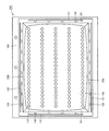
- FIG. 1 is a plan view showing a configuration of a liquid crystal display device including a backlight unit according to Embodiment 1 of the present invention.
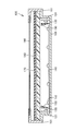
- FIG. 2 is a view as seen from the direction of arrows II-II in FIG.
- the diffusion plate 170, the plurality of optical sheets 180, the liquid crystal display panel 190, and the upper bezel 161 are not shown.
- a liquid crystal display device 100 including a backlight unit according to Embodiment 1 of the present invention is a first light source LED 110, a mounting substrate 140 on which the LED 110 is mounted, and a second light source.
- the main surface of the liquid crystal display panel 190 is a display surface that is an irradiation surface.
- the backlight unit includes an LED 110, a mounting board 140, an LED 120, a mounting board 121, an LED 130, a mounting board 131, and light guides 150 and 151.
- the rectangular lower bezel 160 has a concave shape in which the bottom of the center portion is lower than the edge portion.
- the bottom surface of the center portion of the lower bezel 160 faces the display surface of the liquid crystal display device 100.
- the mounting substrate 140 is placed on the bottom surface at the center of the lower bezel 160.
- a thin film is formed on the upper surface of the mounting substrate 140 by a printing method or the like. This thin film functions as a reflective film that reflects light.
- a plurality of LEDs 110 are arranged in a matrix on the upper surface of the mounting substrate 140. Each of the plurality of LEDs 110 irradiates light in a direction orthogonal to the upper surface of the mounting substrate 140. In other words, the plurality of LEDs 110 are positioned at a predetermined interval on the facing surface facing the display surface of the liquid crystal display device 100, and irradiate light toward the display surface of the liquid crystal display device 100.
- a plurality of LEDs 120 and 130 are arranged in four directions so as to surround the outside of the plurality of LEDs 110. Specifically, two mounting boards 121 are arranged so as to face each other in the vertical direction in FIG. A plurality of LEDs 120 are arranged at predetermined intervals on each of the opposing surfaces of the two mounting boards 121.
- the two mounting boards 131 are arranged so as to face each other in the left-right direction in FIG.
- a plurality of LEDs 130 are arranged at predetermined intervals on each of the opposing surfaces of the two mounting boards 131.
- each main surface of the two mounting boards 121 When each main surface of the two mounting boards 121 is extended, the surface is orthogonal to the display surface of the liquid crystal display device 100.
- Each of the plurality of LEDs 120 irradiates light in a direction orthogonal to the main surface of the mounting substrate 121. In other words, the plurality of LEDs 120 irradiate light in a direction along the display surface of the liquid crystal display device 100.
- the two mounting substrates 131 are orthogonal to the display surface of the liquid crystal display device 100.
- Each of the plurality of LEDs 130 irradiates light in a direction orthogonal to the main surface of the mounting substrate 131. In other words, the plurality of LEDs 130 irradiate light in a direction along the display surface of the liquid crystal display device 100.
- a light guide 150 is disposed between the LED 110 and the LED 120. As shown in FIG. 2, the light guide 150 has a triangular cross-sectional shape. Specifically, the light guide 150 has an incident surface that faces the mounting substrate 121, an emission surface that faces the display surface of the liquid crystal display device 100, and a side surface that faces the plurality of LEDs 110. The incident surface of the light guide 150 and the LED 120 are positioned at a predetermined interval. The plurality of LEDs 120 are located along the incident surface of the light guide 150.
- the light guide 150 Since the light guide 150 has the above-described structure, the light emitted from the LED 120 enters from the incident surface, propagates while repeating total reflection in the light guide 150, and is emitted from the output surface to the liquid crystal display device 100. It emits toward the end of the display surface in the vertical direction.
- a light guide 151 is disposed between the LED 110 and the LED 130. As shown in FIG. 2, the light guide 151 has a triangular cross-sectional shape. Specifically, the light guide 151 has an incident surface that faces the mounting substrate 131, an emission surface that faces the display surface of the liquid crystal display device 100, and a side surface that faces the plurality of LEDs 110. The incident surface of the light guide 151 and the LED 130 are located at a predetermined interval. The plurality of LEDs 130 are positioned along the incident surface of the light guide 151.
- the light guide 151 Since the light guide 151 has the above-described structure, the light emitted from the LED 130 enters from the incident surface, propagates while repeating total reflection in the light guide 151, and is transmitted from the output surface to the liquid crystal display device 100. It emits toward the end of the display surface in the left-right direction.
- the two light guides 150 and the two light guides 151 are arranged in a frame shape with their ends in contact with each other.
- the LEDs 120 and 130 that are the second light sources are located along the outer periphery of the light guides 150 and 151.
- Polymethyl methacrylate is used as the material of the light guide.
- a diffusion plate 170 is placed on the edge of the lower bezel 160.
- the diffusing plate 170 is positioned to face the emission surfaces of the light guides 150 and 151 and diffuses light emitted from the emission surfaces of the light guides 150 and 151.
- a plurality of optical sheets 180 are arranged above the diffusion plate 170.
- the plurality of optical sheets 180 are positioned to face the diffusion plate 170 and have at least one of a function of condensing the light transmitted through the diffusion plate 170 and a function of diffusing.
- the plurality of optical sheets 180 include, for example, a prism sheet and a diffusion sheet.
- a liquid crystal display panel 190 is disposed above the plurality of optical sheets 180.
- the liquid crystal display panel 190 includes an active matrix substrate, a color filter, a counter substrate, and liquid crystal sealed between the active matrix substrate and the counter substrate.
- a plurality of TFT (thin film transistor) elements are formed on the active matrix substrate.
- the liquid crystal display panel 190 displays an image using light that passes through the diffusion plate 170 and the plurality of optical sheets 180 and enters the liquid crystal display panel 190.
- the liquid crystal display panel 190 is supported by the upper bezel 161.
- the upper bezel 161 has a frame shape and has a window portion that allows the display area of the liquid crystal display panel 190 to be visually recognized.
- the upper bezel 161 and the lower bezel 160 are combined to form the casing of the liquid crystal display device 100.
- the light emitted from the LED 120 and the LED 130 compensates for the luminance at the edge of the display surface of the liquid crystal display device 100 where the luminance of the light emitted from the LED 110 is reduced, and the display surface of the liquid crystal display device 100 The uniformity of the brightness at is improved. As a result, the display quality of the liquid crystal display device 100 is improved.
- the plurality of LEDs 120 and 130 as the second light source are arranged around the plurality of LEDs 110 as the first light source.
- the arrangement of the second light source is not limited to this, and the irradiation of the first light source is performed. It suffices that at least one second light source and light guide are arranged so as to compensate for light of a portion having low luminance in the plane.
- the light guide may be divided so as to correspond to each LED.
- both the first light source and the second light source are configured by LEDs, but one of the first light source and the second light source is an LED or a cold cathode fluorescent lamp, and the other is another light source. May be.
- the diffusion plate 170 is provided.
- the optical sheet 180 also functions as the diffusion plate 170, the diffusion plate 170 may not be provided. In that case, the optical sheet 180 is positioned to face the emission surfaces of the light guides 150 and 151.
- the backlight unit according to Embodiment 2 of the present invention will be described. Since the backlight unit of the present embodiment is different from the backlight unit of the first embodiment only in the shape of the light guide, the description of other configurations will not be repeated.
- FIG. 3 is a plan view showing a configuration of a liquid crystal display device including a backlight unit according to Embodiment 2 of the present invention.
- the diffusion plate 170, the plurality of optical sheets 180, the liquid crystal display panel 190, and the upper bezel 161 are not shown.
- a light guide body 250 is disposed between the LED 110 and the LED 120.
- a light guide 251 is disposed between the LED 110 and the LED 130.
- the light guide 250 has a triangular cross-sectional shape. Specifically, the light guide 250 has an incident surface that faces the mounting substrate 121, an emission surface that faces the display surface of the liquid crystal display device 200, and a side surface that faces the plurality of LEDs 110. The incident surface of the light guide 250 and the LED 120 are located at a predetermined interval. The plurality of LEDs 120 are positioned along the incident surface of the light guide body 250.
- the side surface of the light guide 250 is convexly curved toward the LED 120 in a plan view.
- the light guide 251 has a triangular cross-sectional shape. Specifically, the light guide 251 has an incident surface that faces the mounting substrate 131, an emission surface that faces the display surface of the liquid crystal display device 200, and a side surface that faces the plurality of LEDs 110. The incident surface of the light guide 251 and the LED 130 are located at a predetermined interval. The plurality of LEDs 130 are positioned along the incident surface of the light guide 251.
- the side surface of the light guide 251 is curved in a convex shape toward the LED 130 in a plan view.
- the two light guides 250 and the two light guides 251 are arranged in a frame shape with their end portions in contact with each other.
- the LEDs 120 and 130 as the second light sources are located along the outer periphery of the light guides 250 and 251.
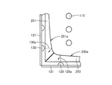
- FIG. 4 is a partial plan view showing an optical path through which light emitted from the second light source propagates in the light guide in the backlight unit according to the present embodiment.
- a part of light irradiated from LED is shown as an example.
- the light 120 a emitted from the LED 120 is reflected by the side surface 250 a of the light guide 250 and propagates toward the end of the light guide 250.
- the light 130 a irradiated from the LED 130 is reflected by the side surface 251 a of the light guide 251 and propagates toward the end of the light guide 251.
- the side surfaces 250a and 251a of the light guides 250 and 251 are curved, the light emitted from the second light source can be collected at the ends of the light guides 250 and 251. As a result, it is possible to increase the light emitted from the emission surfaces at the ends of the light guides 250 and 251.
- the light emitted from the LED 120 and the LED 130 compensates for the luminance at the four corners of the display surface of the liquid crystal display device 200 where the luminance of the light emitted from the LED 110 is reduced, so The uniformity of the brightness at is improved. As a result, the display quality of the liquid crystal display device 200 is improved.
- the heights of the light guides 250 and 251 are made constant, but the lengthwise central portions of the light guides 250 and 251 may be lowered and the ends may be raised. Even in this case, the light emitted from the second light source can be collected at the ends of the light guides 250 and 251.
- the backlight unit according to Embodiment 3 of the present invention will be described. Since the backlight unit of the present embodiment is different from the backlight unit of the first embodiment only in the configuration of the mounting substrate for the second light source, the description of other configurations will not be repeated.
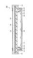
- FIG. 5 is a cross-sectional view showing a configuration of a liquid crystal display device including a backlight unit according to Embodiment 3 of the present invention.
- the mounting substrate 321 on which the LED 320 as the second light source is mounted is placed on the mounting substrate 140. Is done.
- a circuit that can be connected to a circuit provided on the mounting substrate 140 is provided on a side surface of the mounting substrate 321.
- the light guide 150 is also disposed on the mounting substrate 140. All the mounting boards on which LEDs (not shown) are mounted are mounted on the mounting board 140 and connected to the mounting board 140.
- the backlight unit can be integrally formed on the mounting substrate 140, workability when the backlight unit is assembled to the liquid crystal display device 300 can be facilitated.
- liquid crystal display device 110, 120, 130, 320 LED, 120a, 130a light, 121, 131, 140, 321 mounting substrate, 150, 151, 250, 251 light guide, 160 lower bezel, 161 Upper bezel, 170 diffuser plate, 180 optical sheet, 190 liquid crystal display panel, 250a, 251a side.
Landscapes
- Physics & Mathematics (AREA)
- Nonlinear Science (AREA)
- Mathematical Physics (AREA)
- Chemical & Material Sciences (AREA)
- Crystallography & Structural Chemistry (AREA)
- General Physics & Mathematics (AREA)
- Optics & Photonics (AREA)
- Engineering & Computer Science (AREA)
- Multimedia (AREA)
- Signal Processing (AREA)
- Planar Illumination Modules (AREA)
Abstract
液晶表示装置(100)の照射面に対向する対向面上に所定の間隔を置いて位置し、照射面に向けて光を照射する複数の第1光源(110)と、複数の第1光源(110)の外側に位置し、照射面に沿う方向に向けて光を照射する第2光源(120,130)とを備える。また、第1光源(110)と第2光源(120,130)との間に位置し、第2光源(120,130)から照射された光が入射面から入射して出射面から照射面の端部に向けて出射するように、第2光源(120,130)と所定の間隔を置いて位置する導光体(150,151)を備えている。
Description
本発明は、照明装置、それを備えた表示装置、およびそれを備えたテレビ受信装置に関する。
直下型バックライトユニットの構成を開示した先行文献として、特開2008-96492号公報(特許文献1)がある。特許文献1に記載されたLED(Light Emitting Diode)バックライトユニットにおいては、筐体の底面側に反射板が配置され、その上面側に複数のLEDがマトリックス状に配設されている。
直下型バックライトユニットでは、複数のLEDから光が照射される照射面内において、光の輝度が中心部に比べて端部で低くなる。このような輝度ムラを有する直下型バックライトユニットを表示装置に設けた場合、表示装置の表示面内の端部が暗くなり表示品質が低下する。
本発明は上記の問題点に鑑みてなされたものであって、照射面内における輝度の均一性を向上できる、照明装置、それを備えた表示装置、およびそれを備えたテレビ受信装置を提供することを目的とする。
本発明に基づく照明装置は、面発光して照射面を照らす照明装置である。バックライトユニットは、上記照射面に対向する対向面上に所定の間隔を置いて位置し、上記照射面に向けて光を照射する複数の第1光源と、複数の第1光源の外側に位置し、上記照射面に沿う方向に向けて光を照射する第2光源とを備える。また、バックライトユニットは、第1光源と第2光源との間に位置し、第2光源から照射された光が入射面から入射して出射面から上記照射面の端部に向けて出射するように、第2光源と所定の間隔を置いて位置する導光体を備えている。
本発明の一形態においては、第2光源が、導光体の入射面に沿って複数位置している。導光体の複数の第1光源と面する側の側面は、第2光源側に凸状に湾曲している。
本発明の一形態においては、導光体が、複数の第1光源の四方を囲むように位置している。第2光源が、導光体の外周に沿って位置している。
本発明の一形態においては、第1光源および第2光源の少なくとも一方がLEDである。
本発明の一形態においては、第1光源および第2光源の少なくとも一方が冷陰極蛍光ランプである。
本発明の一形態においては、導光体の出射面と対向して位置し、導光体の出射面から出射した光を拡散する拡散板と、拡散板と対向して位置し、拡散板を透過した光を集光する機能および拡散する機能の少なくともいずれかを有する光学シートとをさらに備えている。
本発明の一形態においては、導光体の出射面と対向して位置し、導光体の出射面から出射した光を集光する機能および拡散する機能の少なくともいずれかを有する光学シートとをさらに備えている。
本発明によれば、照射面内における輝度の均一性を向上できる。
以下、本発明の実施形態1に係る照明装置、それを備えた表示装置、およびそれを備えたテレビ受信装置について説明する。以下の実施形態の説明においては、図中の同一または相当部分には同一符号を付して、その説明は繰り返さない。
なお、実施形態の説明において、説明の便宜上、上、下、左、右の表現を用いるが、これらの表現は示した図に基づくものであって発明の構成を限定するものではない。また、実施形態においては、液晶表示装置のバックライトユニットに本発明を適用した場合について説明するが、本発明は、液晶表示装置以外の他の表示装置、それを備えたテレビ受信装置または照明装置単体などにも適用可能である。
(実施形態1)
図1は、本発明の実施形態1に係るバックライトユニットを含む液晶表示装置の構成を示す平面図である。図2は、図1のII-II線矢印方向から見た図である。なお、図1においては、簡単のため、拡散板170、複数の光学シート180、液晶表示パネル190および上側ベゼル161を図示していない。
図1は、本発明の実施形態1に係るバックライトユニットを含む液晶表示装置の構成を示す平面図である。図2は、図1のII-II線矢印方向から見た図である。なお、図1においては、簡単のため、拡散板170、複数の光学シート180、液晶表示パネル190および上側ベゼル161を図示していない。
図1,2に示すように、本発明の実施形態1に係るバックライトユニットを含む液晶表示装置100は、第1光源であるLED110、LED110を搭載している実装基板140、第2光源であるLED120、LED120を搭載している実装基板121、第2光源であるLED130、LED130を搭載している実装基板131、導光体150,151、下側ベゼル160、拡散板170、複数の光学シート180、液晶表示パネル190、および、上側ベゼル161を備えている。液晶表示装置100において、液晶表示パネル190の主面が照射面である表示面となる。
本実施形態に係るバックライトユニットは、LED110、実装基板140、LED120、実装基板121、LED130、実装基板131、導光体150,151を含む。
平面視において矩形状の下側ベゼル160は、縁部に対して中央部の底が低くなった凹状の形状を有している。下側ベゼル160の中央部の底面は、液晶表示装置100の表示面と対向している。下側ベゼル160の中央部の底面上に実装基板140が載置されている。
実装基板140の上面には、印刷法などによって薄膜が形成されている。この薄膜は、光を反射する反射膜として機能する。また、実装基板140の上面に、複数のLED110がマトリックス状に配置されている。複数のLED110の各々は、実装基板140の上面に直交する方向に光を照射する。言い換えると、複数のLED110は、液晶表示装置100の表示面に対向する対向面上に所定の間隔を置いて位置し、液晶表示装置100の表示面に向けて光を照射する。
複数のLED110の外側を取り囲むように四方に複数のLED120,130が配置されている。具体的には、図1中の上下方向において互いに対向するように2つの実装基板121が配置されている。2つの実装基板121の互いに対向する対向面の各々には、所定の間隔を置いて複数のLED120が配置されている。
図1中の左右方向において互いに対向するように2つの実装基板131が配置されている。2つの実装基板131の互いに対向する対向面の各々には、所定の間隔を置いて複数のLED130が配置されている。
2つの実装基板121の各々の主面を延長すると、液晶表示装置100の表示面に対して直交する。複数のLED120の各々は、実装基板121の主面に直交する方向に光を照射する。言い換えると、複数のLED120は、液晶表示装置100の表示面に沿う方向に向けて光を照射する。
2つの実装基板131の各々の主面を延長すると、液晶表示装置100の表示面に対して直交する。複数のLED130の各々は、実装基板131の主面に直交する方向に光を照射する。言い換えると、複数のLED130は、液晶表示装置100の表示面に沿う方向に向けて光を照射する。
LED110とLED120との間に導光体150が配置されている。図2に示すように、導光体150は、三角形状の横断面形状を有している。具体的には、導光体150は、実装基板121と対向する入射面と、液晶表示装置100の表示面と対向する出射面と、複数のLED110と面する側面とを有している。導光体150の入射面とLED120とは、所定の間隔を置いて位置している。複数のLED120は、導光体150の入射面に沿って位置している。
導光体150が上記の構造を有することにより、LED120から照射された光は、入射面から入射して、導光体150内で全反射を繰り返しながら伝播して、出射面から液晶表示装置100の表示面の上下方向における端部に向けて出射する。
LED110とLED130との間に導光体151が配置されている。図2に示すように、導光体151は、三角形状の横断面形状を有している。具体的には、導光体151は、実装基板131と対向する入射面と、液晶表示装置100の表示面と対向する出射面と、複数のLED110と面する側面とを有している。導光体151の入射面とLED130とは、所定の間隔を置いて位置している。複数のLED130は、導光体151の入射面に沿って位置している。
導光体151が上記の構造を有することにより、LED130から照射された光は、入射面から入射して、導光体151内で全反射を繰り返しながら伝播して、出射面から液晶表示装置100の表示面の左右方向における端部に向けて出射する。
2つの導光体150と2つの導光体151とは、互いの端部同士が接触して枠状に配置されている。第2光源であるLED120,130は、導光体150,151の外周に沿って位置している。導光体の材料としては、ポリメタクリル酸メチルを用いている。
下側ベゼル160の縁部上に拡散板170が載置されている。拡散板170は、導光体150,151の出射面と対向して位置し、導光体150,151の出射面から出射した光を拡散する。
拡散板170の上方に複数の光学シート180が配置されている。複数の光学シート180は、拡散板170と対向して位置し、拡散板170を透過した光を集光する機能および拡散する機能の少なくともいずれかを有する。複数の光学シート180は、たとえば、プリズムシートおよび拡散シートなどを含む。
複数の光学シート180の上方に液晶表示パネル190が配置されている。液晶表示パネル190は、アクティブマトリックス基板と、カラーフィルタと、対向基板と、アクティブマトリックス基板および対向基板の間に封入された液晶とを含む。アクティブマトリックス基板には、複数のTFT(thin film transistor)素子が形成されている。液晶表示パネル190は、拡散板170および複数の光学シート180を通過して液晶表示パネル190に入射する光を用いて画像を表示する。
液晶表示パネル190は、上側ベゼル161に支持されている。上側ベゼル161は、枠状の形状を有し、液晶表示パネル190の表示領域を視認可能とする窓部を有している。上側ベゼル161と下側ベゼル160とが組み合わされて、液晶表示装置100の筐体が構成されている。
上記の構成により、LED120およびLED130から照射された光が、LED110から照射された光の輝度が低くなる液晶表示装置100の表示面の端部の輝度を補って、液晶表示装置100の表示面内における輝度の均一性が向上される。その結果、液晶表示装置100の表示品質が向上する。
なお、本実施形態においては、第1光源である複数のLED110の周囲に第2光源である複数のLED120,130を配置したが、第2光源の配置はこれに限られず、第1光源の照射面内において輝度の低い部分の光を補えるように少なくとも1つの第2光源および導光体が配置されていればよい。
また、エリア点灯(2D/3D-Dimming)可能なバックライトユニットにおいては、導光体を分割して各LEDに対応するように配置してもよい。
さらに、本実施形態においては、第1光源および第2光源の両方をLEDで構成したが、第1光源および第2光源の一方がLEDまたは冷陰極蛍光ランプであり、他方が他の光源であってもよい。
本実施形態においては、拡散板170を設けたが光学シート180が拡散板170の機能を兼ねる場合には拡散板170を設けなくてもよい。その場合、光学シート180は、導光体150,151の出射面と対向して位置している。
以下、本発明の実施形態2に係るバックライトユニットについて説明する。本実施形態のバックライトユニットは、導光体の形状のみ実施形態1のバックライトユニットと異なるため、他の構成については説明を繰り返さない。
(実施形態2)
図3は、本発明の実施形態2に係るバックライトユニットを含む液晶表示装置の構成を示す平面図である。なお、図3においては、簡単のため、拡散板170、複数の光学シート180、液晶表示パネル190および上側ベゼル161を図示していない。
図3は、本発明の実施形態2に係るバックライトユニットを含む液晶表示装置の構成を示す平面図である。なお、図3においては、簡単のため、拡散板170、複数の光学シート180、液晶表示パネル190および上側ベゼル161を図示していない。
図3に示すように、本発明の実施形態2に係るバックライトユニットを含む液晶表示装置200においては、LED110とLED120との間に導光体250が配置されている。LED110とLED130との間に導光体251が配置されている。
導光体250は、三角形状の横断面形状を有している。具体的には、導光体250は、実装基板121と対向する入射面と、液晶表示装置200の表示面と対向する出射面と、複数のLED110と面する側面とを有している。導光体250の入射面とLED120とは、所定の間隔を置いて位置している。複数のLED120は、導光体250の入射面に沿って位置している。
図3に示すように、導光体250の上記側面は、平面視において、LED120側に凸状に湾曲している。
導光体251は、三角形状の横断面形状を有している。具体的には、導光体251は、実装基板131と対向する入射面と、液晶表示装置200の表示面と対向する出射面と、複数のLED110と面する側面とを有している。導光体251の入射面とLED130とは、所定の間隔を置いて位置している。複数のLED130は、導光体251の入射面に沿って位置している。
図3に示すように、導光体251の上記側面は、平面視において、LED130側に凸状に湾曲している。
2つの導光体250と2つの導光体251とは、互いの端部同士が接触して枠状に配置されている。第2光源であるLED120,130は、導光体250,251の外周に沿って位置している。
図4は、本実施形態に係るバックライトユニットにおいて第2光源から照射された光が導光体内を伝播する光路を示す一部平面図である。なお、図4においては、LEDから照射された光の一部を例示的に示している。
図4に示すように、LED120から照射された光120aは、導光体250の側面250aで反射されて導光体250の端部に向けて伝播する。同様に、LED130から照射された光130aは、導光体251の側面251aで反射されて導光体251の端部に向けて伝播する。
このように、導光体250,251の側面250a,251aが湾曲していることにより、第2光源から照射された光を導光体250,251の端部に集めることができる。その結果、導光体250,251の端部の出射面から出射する光を多くすることができる。
上記の構成により、LED120およびLED130から照射された光が、LED110から照射された光の輝度が低くなる液晶表示装置200の表示面の四隅部の輝度を補って、液晶表示装置200の表示面内における輝度の均一性が向上される。その結果、液晶表示装置200の表示品質が向上する。
本実施形態においては、導光体250,251の高さを一定にしたが、導光体250,251の長さ方向の中央部を低くして、端部を高くしてもよい。このようにした場合にも、第2光源から照射された光を導光体250,251の端部に集めることができる。
以下、本発明の実施形態3に係るバックライトユニットについて説明する。本実施形態のバックライトユニットは、第2光源の実装基板の構成のみ実施形態1のバックライトユニットと異なるため、他の構成については説明を繰り返さない。
(実施形態3)
図5は、本発明の実施形態3に係るバックライトユニットを含む液晶表示装置の構成を示す断面図である。図5に示すように、本発明の実施形態3に係るバックライトユニットを含む液晶表示装置300においては、第2光源であるLED320を搭載している実装基板321が、実装基板140上に載置される。具体的には、実装基板321の側面に、実装基板140に設けられた回路と接続可能な回路が設けられている。また、導光体150も実装基板140上に配置されている。なお、図示していないLEDを搭載している全ての実装基板は、実装基板140上に載置されて実装基板140に接続されている。
図5は、本発明の実施形態3に係るバックライトユニットを含む液晶表示装置の構成を示す断面図である。図5に示すように、本発明の実施形態3に係るバックライトユニットを含む液晶表示装置300においては、第2光源であるLED320を搭載している実装基板321が、実装基板140上に載置される。具体的には、実装基板321の側面に、実装基板140に設けられた回路と接続可能な回路が設けられている。また、導光体150も実装基板140上に配置されている。なお、図示していないLEDを搭載している全ての実装基板は、実装基板140上に載置されて実装基板140に接続されている。
上記の構成により、バックライトユニットを実装基板140に一体的に構成できるため、液晶表示装置300にバックライトユニットを組み付ける際の作業性を容易にすることができる。
今回開示された実施形態はすべての点で例示であって制限的なものではないと考えられるべきである。本発明の範囲は上記した説明ではなくて請求の範囲によって示され、請求の範囲と均等の意味および範囲内でのすべての変更が含まれることが意図される。
100,200,300 液晶表示装置、110,120,130,320 LED、120a,130a 光、121,131,140,321 実装基板、150,151,250,251 導光体、160 下側ベゼル、161 上側ベゼル、170 拡散板、180 光学シート、190 液晶表示パネル、250a,251a 側面。
Claims (9)
- 面発光して照射面を照らす照明装置であって、
前記照射面に対向する対向面上に所定の間隔を置いて位置し、前記照射面に向けて光を照射する複数の第1光源と、
前記複数の第1光源の外側に位置し、前記照射面に沿う方向に向けて光を照射する第2光源と、
前記第1光源と前記第2光源との間に位置し、前記第2光源から照射された光が入射面から入射して出射面から前記照射面の端部に向けて出射するように、前記第2光源と所定の間隔を置いて位置する導光体(150,151,250,251)と
を備えた、照明装置。 - 前記第2光源が、前記導光体の前記入射面に沿って複数位置し、
前記導光体(250,251)の前記複数の第1光源と面する側の側面は、前記第2光源側に凸状に湾曲している、請求項1に記載の照明装置。 - 前記導光体(150,151,250,251)が、前記複数の第1光源の四方を囲むように位置し、
前記第2光源が、前記導光体(150,151,250,251)の外周に沿って位置している、請求項1または2に記載の照明装置。 - 前記第1光源および前記第2光源の少なくとも一方がLEDである、請求項1から3のいずれかに記載の照明装置。
- 前記第1光源および前記第2光源の少なくとも一方が冷陰極蛍光ランプである、請求項1から3のいずれかに記載の照明装置。
- 前記導光体(150,151,250,251)の前記出射面と対向して位置し、前記導光体の前記出射面から出射した光を拡散する拡散板(170)と、
前記拡散板(170)と対向して位置し、前記拡散板(170)を透過した光を集光する機能および拡散する機能の少なくともいずれかを有する光学シート(180)と
をさらに備えた、請求項1から5のいずれかに記載の照明装置。 - 前記導光体(150,151,250,251)の前記出射面と対向して位置し、前記導光体(150,151,250,251)の前記出射面から出射した光を拡散する機能を有する光学シート(180)をさらに備えた、請求項1から5のいずれかに記載の照明装置。
- 請求項1から7のいずれかに記載の照明装置と、
前記照明装置から照射された光を用いて画像を表示する表示パネル(190)と
を備えた、表示装置。 - 請求項8に記載の表示装置(100,200,300)を備えた、テレビ受信装置。
Applications Claiming Priority (2)
| Application Number | Priority Date | Filing Date | Title |
|---|---|---|---|
| JP2011113820 | 2011-05-20 | ||
| JP2011-113820 | 2011-05-20 |
Publications (1)
| Publication Number | Publication Date |
|---|---|
| WO2012161014A1 true WO2012161014A1 (ja) | 2012-11-29 |
Family
ID=47217094
Family Applications (1)
| Application Number | Title | Priority Date | Filing Date |
|---|---|---|---|
| PCT/JP2012/062287 Ceased WO2012161014A1 (ja) | 2011-05-20 | 2012-05-14 | 照明装置、それを備えた表示装置、およびそれを備えたテレビ受信装置 |
Country Status (1)
| Country | Link |
|---|---|
| WO (1) | WO2012161014A1 (ja) |
Citations (2)
| Publication number | Priority date | Publication date | Assignee | Title |
|---|---|---|---|---|
| JP2008166296A (ja) * | 2008-03-10 | 2008-07-17 | Sharp Corp | 照明装置 |
| JP2009238566A (ja) * | 2008-03-27 | 2009-10-15 | Epson Imaging Devices Corp | 照明装置、液晶装置及び電子機器 |
-
2012
- 2012-05-14 WO PCT/JP2012/062287 patent/WO2012161014A1/ja not_active Ceased
Patent Citations (2)
| Publication number | Priority date | Publication date | Assignee | Title |
|---|---|---|---|---|
| JP2008166296A (ja) * | 2008-03-10 | 2008-07-17 | Sharp Corp | 照明装置 |
| JP2009238566A (ja) * | 2008-03-27 | 2009-10-15 | Epson Imaging Devices Corp | 照明装置、液晶装置及び電子機器 |
Similar Documents
| Publication | Publication Date | Title |
|---|---|---|
| CN101680636B (zh) | 照明装置和液晶显示装置 | |
| US8579456B2 (en) | Backlight unit | |
| CN110058452B (zh) | 照明装置和显示装置 | |
| KR100999780B1 (ko) | 광학 어셈블리, 이를 구비한 백라이트 유닛 및 디스플레이 장치 | |
| WO2011070724A1 (ja) | 照明装置及びそれを備えた液晶表示装置 | |
| WO2011093119A1 (ja) | 照明装置、表示装置、テレビ受信装置 | |
| TWI436132B (zh) | 背光單元及使用該背光單元的顯示裝置 | |
| CN202972587U (zh) | 照明装置、显示装置以及电视接收装置 | |
| WO2012032978A1 (ja) | 反射シート、照明装置および表示装置 | |
| JP5108953B2 (ja) | 照明装置、表示装置、及びテレビ受信装置 | |
| JP4607225B2 (ja) | 光源モジュール、液晶表示装置および照明装置 | |
| KR20140011104A (ko) | 백라이트 유닛 및 이를 포함하는 액정 표시 장치 | |
| JP5073834B2 (ja) | 照明装置、表示装置、及びテレビ受信装置 | |
| JP6846944B2 (ja) | 面状光源装置および表示装置 | |
| CN105683789A (zh) | 背光装置和显示装置 | |
| KR101983312B1 (ko) | 백라이트 유닛 및 이를 포함하는 액정표시장치 | |
| WO2010041499A1 (ja) | 照明装置、表示装置、及びテレビ受信装置 | |
| WO2012026164A1 (ja) | 照明装置および表示装置 | |
| WO2012063917A1 (ja) | 照明装置およびこれを備えた液晶表示装置 | |
| KR20090053631A (ko) | 백라이트 유닛, 이를 구비한 액정표시장치 및 그 제조방법 | |
| WO2012035840A1 (ja) | 照明装置およびこれを備えた液晶表示装置 | |
| KR101839335B1 (ko) | 백 라이트 유닛 및 이를 이용한 액정 표시장치 | |
| WO2012161014A1 (ja) | 照明装置、それを備えた表示装置、およびそれを備えたテレビ受信装置 | |
| KR100664373B1 (ko) | 백색 발광다이오드를 채택한 백라이트 패널 | |
| WO2012102096A1 (ja) | エッジライト型照明装置及び表示装置 |
Legal Events
| Date | Code | Title | Description |
|---|---|---|---|
| 121 | Ep: the epo has been informed by wipo that ep was designated in this application |
Ref document number: 12789150 Country of ref document: EP Kind code of ref document: A1 |
|
| NENP | Non-entry into the national phase |
Ref country code: DE |
|
| 122 | Ep: pct application non-entry in european phase |
Ref document number: 12789150 Country of ref document: EP Kind code of ref document: A1 |
|
| NENP | Non-entry into the national phase |
Ref country code: JP |