WO2012160910A1 - 圧電駆動素子及び圧電駆動装置 - Google Patents
圧電駆動素子及び圧電駆動装置 Download PDFInfo
- Publication number
- WO2012160910A1 WO2012160910A1 PCT/JP2012/060409 JP2012060409W WO2012160910A1 WO 2012160910 A1 WO2012160910 A1 WO 2012160910A1 JP 2012060409 W JP2012060409 W JP 2012060409W WO 2012160910 A1 WO2012160910 A1 WO 2012160910A1
- Authority
- WO
- WIPO (PCT)
- Prior art keywords
- piezoelectric
- ceramic
- piezoelectric ceramic
- composite
- resonance frequency
- Prior art date
- Legal status (The legal status is an assumption and is not a legal conclusion. Google has not performed a legal analysis and makes no representation as to the accuracy of the status listed.)
- Ceased
Links
Images



Classifications
-
- H—ELECTRICITY
- H10—SEMICONDUCTOR DEVICES; ELECTRIC SOLID-STATE DEVICES NOT OTHERWISE PROVIDED FOR
- H10N—ELECTRIC SOLID-STATE DEVICES NOT OTHERWISE PROVIDED FOR
- H10N30/00—Piezoelectric or electrostrictive devices
- H10N30/80—Constructional details
- H10N30/85—Piezoelectric or electrostrictive active materials
- H10N30/852—Composite materials, e.g. having 1-3 or 2-2 type connectivity
-
- H—ELECTRICITY
- H10—SEMICONDUCTOR DEVICES; ELECTRIC SOLID-STATE DEVICES NOT OTHERWISE PROVIDED FOR
- H10N—ELECTRIC SOLID-STATE DEVICES NOT OTHERWISE PROVIDED FOR
- H10N30/00—Piezoelectric or electrostrictive devices
- H10N30/01—Manufacture or treatment
- H10N30/05—Manufacture of multilayered piezoelectric or electrostrictive devices, or parts thereof, e.g. by stacking piezoelectric bodies and electrodes
- H10N30/053—Manufacture of multilayered piezoelectric or electrostrictive devices, or parts thereof, e.g. by stacking piezoelectric bodies and electrodes by integrally sintering piezoelectric or electrostrictive bodies and electrodes
-
- H—ELECTRICITY
- H10—SEMICONDUCTOR DEVICES; ELECTRIC SOLID-STATE DEVICES NOT OTHERWISE PROVIDED FOR
- H10N—ELECTRIC SOLID-STATE DEVICES NOT OTHERWISE PROVIDED FOR
- H10N30/00—Piezoelectric or electrostrictive devices
- H10N30/01—Manufacture or treatment
- H10N30/09—Forming piezoelectric or electrostrictive materials
- H10N30/092—Forming composite materials
-
- H—ELECTRICITY
- H10—SEMICONDUCTOR DEVICES; ELECTRIC SOLID-STATE DEVICES NOT OTHERWISE PROVIDED FOR
- H10N—ELECTRIC SOLID-STATE DEVICES NOT OTHERWISE PROVIDED FOR
- H10N30/00—Piezoelectric or electrostrictive devices
- H10N30/50—Piezoelectric or electrostrictive devices having a stacked or multilayer structure
Definitions
- the present invention relates to a piezoelectric driving element and a piezoelectric driving device, and more specifically to a piezoelectric driving element and a piezoelectric driving device used at and near a resonance frequency.
- a resonant actuator 200 shown in FIG. 7A has a configuration in which electrodes 204a and 204b are provided on both end faces of a piezoelectric ceramic body 202 formed in a square bar shape.
- the resonance actuator 200 is polarized in the direction of arrow a, and is driven at a resonance frequency or a frequency near the resonance frequency by applying an AC electric field to the electrodes 204a and 204b, and is longitudinal in the direction of arrow b which is the same direction as the polarization direction a. It is configured to obtain vibration.
- the conductive wires 208a and 208b connected to the AC power supply 210 and the electrodes 204a and 204b are connected via the spring terminals 206a and 206b, or the electrodes 204a and 204b are directly connected to the conductive wires 208a and 208b.
- an alternating electric field is applied to the electrodes 204a and 204b.
- FIG. 7B In the resonance actuator 250 shown in FIG. 7B, electrodes 254a and 254b provided on both end faces of a square bar-shaped piezoelectric ceramic body 252 are connected to the side surfaces of the piezoelectric ceramic body 252 by lead conductors 258a and 258b.
- a configuration is disclosed in which vibration inhibition is suppressed by pulling out in the middle and pressing the connection electrodes 256a and 256b by spring terminals 260a and 260b.
- Non-Patent Document 1 in Sadayuki Takahashi's “New Development of Piezoelectric Materials”, TIC Co., Ltd., New Ceramics VOL.11, No.8 (1988), p29-34 (Non-Patent Document 1), in power devices such as piezoelectric actuators, Since the large amplitude elastic vibration of the ceramic is used, the large amplitude characteristics of the piezoelectric ceramic are described.
- Non-Patent Document 2 drives PZT piezoelectric ceramics at resonance frequency.
- the vibration level exceeds a certain value, the resonance frequency fr and the mechanical quality factor decrease.
- a conventional PZT piezoelectric ceramic is used for a resonance actuator, it is known that the resonance frequency and the mechanical quality factor decrease as the vibration speed increases.
- AC voltage of 0.05V, 0.11V, 0.14V, 0.20V, 0.26V, 0.33V is applied to the resonance actuator of PZT-based piezoelectric ceramics, and the drive frequency is changed from above the resonance frequency.
- the resonance frequency indicating the maximum vibration speed shifted to the low frequency side as the amplitude of the AC electric field increased. And even if the frequency was lowered, the vibration speed did not return to the original value and showed hysteresis.
- the bismuth layered compound has low piezoelectric characteristics, there is a problem that when a load is applied to the resonant actuator, the mechanical quality factor is kept low and cannot be driven. Therefore, in piezoelectric ceramics with higher piezoelectric properties than bismuth layered compounds, even when the AC electric field is increased to increase the vibration speed of the piezoelectric drive element, the fluctuation of the resonance frequency is suppressed and the resonance frequency is stabilized. In addition, it is desired to be able to drive near the resonance frequency.
- a piezoelectric driving element and a piezoelectric driving device are provided.
- a piezoelectric driving element has a first piezoelectric ceramic having a soft spring characteristic in which an elastic constant decreases as the vibration speed increases, and a hard spring characteristic in which the elastic constant increases as the vibration speed increases.
- a composite ceramic comprising a composite of the second piezoelectric ceramic and an external electrode provided on a side surface of the composite ceramic so as to face the composite ceramic, wherein the external electrode has a resonance frequency. And an AC electric field in the vicinity of the resonance frequency is applied for driving.
- the composite ceramic includes a configuration in which the first piezoelectric ceramic and the second piezoelectric ceramic are mixed, or the first piezoelectric ceramic and the second piezoelectric ceramic. It has a layered structure. In another embodiment, the composite ceramic has a configuration in which the first piezoelectric ceramic and the second piezoelectric ceramic are layered in a planar shape, a roll shape, or a concentric shape. . In still another embodiment, a multilayer structure is formed by providing a plurality of internal electrodes connected to each of the opposing external electrodes inside the composite ceramic. In still another embodiment, the elastic constant of the composite ceramic is adjusted by the volume fraction of the first piezoelectric ceramic and the second piezoelectric ceramic to suppress the fluctuation of the resonance frequency with respect to the change in vibration speed. To do.
- the first piezoelectric ceramic is a lead-based piezoelectric ceramic made of PZT, BaTiO 3 , (Ba 1/2 Na 1/2 ) TiO 3 , (Ba 1/2 K 1/2). ) TiO 3 , and ⁇ (K 1 ⁇ x Na x ) 1 ⁇ y Li y ⁇ (Nb 1 ⁇ z ⁇ w Ta z Sb w ) O 3 (0 ⁇ x ⁇ 1, 0 ⁇ y ⁇ 0.2,0 ⁇ z ⁇ 0.4, 0 ⁇ w ⁇ 0.2), or a solid solution ceramic containing at least two of these, wherein the second piezoelectric ceramic is Sr 2 ⁇ x Ca x NaNb 5 O 15 (0 ⁇ x ⁇ 2), Sr 2 NaNb 5 O 15 , Ca 2 NaNb 5 O 15 , Sr 2 KNb 5 O 15 , Ba 2 LiNb 5 O 15 , Ba 2 NaNb 5 O 15 , Ba 2 KNb 5 O 15 , K 3 Li
- the piezoelectric driving element and the piezoelectric driving device that are stably driven near the resonance frequency and the resonance frequency can be obtained.
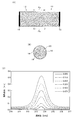
- Example 1 of this invention It is a figure which shows Example 1 of this invention, (A) is principal sectional drawing which shows the structure of a piezoelectric drive element, (B) is a partial enlarged view of the composite ceramic of said (A), (C) is an experiment example. It is a figure which shows the relationship between the vibration speed of 1 and a frequency characteristic. It is a figure which shows the relationship between the vibration speed of the piezoelectric drive element of the comparative example in the said Example 1, and a frequency characteristic, (A) shows the characteristic of the comparative example 1 using the piezoelectric ceramic which has a soft spring characteristic, B) shows the characteristics of Comparative Example 2 using a piezoelectric ceramic having hard spring characteristics.
- FIG. 1A is a main cross-sectional view showing the configuration of the piezoelectric drive element of this embodiment
- FIG. 1B is a partially enlarged view of the composite ceramic of FIG. 1A
- FIG. 2 is a diagram showing the relationship between the vibration speed and frequency characteristics of the piezoelectric drive element of the comparative example.
- A shows the characteristics of comparative example 1 using piezoelectric ceramics having soft spring characteristics.
- a piezoelectric ceramic having hard spring characteristics Shows the characteristics of Comparative Example 2 using a piezoelectric ceramic having hard spring characteristics.
- the piezoelectric driving element 10 of this embodiment includes a first piezoelectric ceramic 18 having a soft spring characteristic in which the elastic constant decreases as the vibration speed increases, and elasticity as the vibration speed increases.
- a first piezoelectric ceramic 18 having a soft spring characteristic in which the elastic constant decreases as the vibration speed increases, and elasticity as the vibration speed increases.
- the second piezoelectric ceramics 20 having a hard spring characteristic with a large constant so as to be orthogonal to the polarization direction (the direction of the arrow Fa in FIG. 1A).
- the external electrodes 14 and 16 are provided.
- the composite ceramic 12 has a form in which the first piezoelectric ceramic 18 and the second piezoelectric ceramic 20 are mixed with powder (partially enlarged view of FIG. 1B). reference). Then, by applying an AC electric field in the vicinity of the resonance frequency from the AC power source (not shown) to the composite ceramics 12 through the external electrodes 14 and 16, the piezoelectric driving element 10 is moved in the direction indicated by the arrow
- the volume fraction of the first piezoelectric ceramic 18 and the second piezoelectric ceramic 20 may be 1, but the change in elastic modulus due to the vibration speed (drive electric field) is suppressed, and the resonance frequency with respect to the vibration speed.
- the volume fraction may be set so as to suppress fluctuations in the above. It is desirable to adjust the fluctuation of the resonance frequency to be, for example, 0.05% or less.
- the first piezoelectric ceramic 18 having the soft spring characteristic for example, a lead-based piezoelectric ceramic made of PZT, BaTiO 3 , (Ba 1/2 Na 1/2 ) TiO 3 , (Ba 1/2).
- the second piezoelectric ceramic 20 of stiff spring characteristic for example, Sr 2-x Ca x NaNb 5 O 15 (0 ⁇ x ⁇ 2), Sr 2 NaNb 5 O 15, Ca 2 NaNb 5 O 15, sr 2 KNb 5 O 15, Ba 2 LiNb 5 O 15, Ba 2 NaNb 5 O 15, Ba 2 KNb 5 O 15, K 3 Li 2 Nb 5 O 15, Ba 2 Bi 1/3 Nb 5 O 15, Pb 2 It is selected from NaNb 5 O 15 , Pb 2 KNb 5 O 15 , or tungsten bronze type solid solution ceramics containing at least two of these.
- the external electrodes 14 and 16 various known electrode materials, for example, Ag are used.
- Example 1 Next, specific examples of this embodiment will be further described.
- a piezoelectric ceramic of (K 0.5 , Na 0.5 ) NbO 3 is selected
- the second piezoelectric ceramic 20 having a hard spring characteristic Sr 1.9 Ca O.S.
- a piezoelectric ceramic of 1 NaNb 5 O 15 was selected.
- Each piezoelectric ceramic powder is prepared by a solid-phase synthesis method in which K 2 CO 3 , Na 2 CO 3 , Nb 2 O 5 , SrCO 3 , and CaCO 3 are weighed in a stoichiometric composition, mixed, and calcined. did.
- Example 1 The same material as in Example 1 was used for the external electrodes provided on the end faces of the piezoelectric ceramics of Comparative Examples 1 and 2.
- the piezoelectric driving element was driven at the resonance frequency and a frequency in the vicinity thereof, and the characteristics were confirmed.
- the applied AC voltage is 0.05V, 0.14V, and 0.1V for the piezoelectric drive element made of the (K 0.5 , Na 0.5 ) NbO 3 piezoelectric ceramic of Comparative Example 1.
- the piezoelectric driving element of Comparative Example 1 has a soft spring characteristic that the resonance frequency decreases and the vibration speed of the piezoelectric driving element increases (increases the amplitude) by increasing the applied AC electric field. showed that.
- FIG. 2 (B) shows Sr 1.9 Ca 2 O.O in Comparative Example 2 .
- the applied AC voltage was 0.06V, 0.16V, 0.23V, 0.37V, 0.43V, 0.48V.
- the measurement results of the vibration speed and frequency when the frequency is raised from a frequency lower than the resonance frequency to a higher frequency are shown.
- the piezoelectric driving element of Comparative Example 2 has a hard spring characteristic that the resonance frequency increases and the vibration speed of the piezoelectric driving element increases (increases the amplitude) by increasing the applied AC electric field. showed that.
- FIG. 1 (C) shows (K 0.5 , Na 0.5 ) NbO 3 piezoelectric ceramics and Sr 1.9 Ca O.3.
- the applied AC voltage is 0.05 V, 0.15 V, 0.20 V, 0.35 V, 0.40 V, and 0.47 V, respectively.
- the measurement result of the vibration speed in the vicinity of the resonance frequency and the resonance frequency is shown.
- Example 1 it has the 1st piezoelectric ceramic 18 which has the soft spring characteristic that an elastic constant becomes small when a vibration speed increases, and the hard spring characteristic that an elastic constant becomes large when a vibration speed increases.
- External electrodes 14 and 16 are provided so as to face the composite ceramic 12 composited with the second piezoelectric ceramic 20 via the composite ceramic 12 and to be orthogonal to the polarization direction, and through the external electrodes 14 and 16.
- the piezoelectric drive element 10 was driven by applying an alternating electric field.
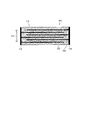
- FIG. 3 is a main cross-sectional view showing the configuration of the piezoelectric drive element of the present embodiment.
- the piezoelectric driving element 30 of this embodiment includes a plurality of internal electrodes 32 connected to the external electrode 14 and a plurality of internal electrodes 34 connected to the external electrode 16 inside the composite ceramic 12. 16 has a laminated structure of internal electrodes arranged alternately in a direction orthogonal to the direction 16.
- Example 2 Next, a specific example of this example will be further described.
- a piezoelectric ceramic of (K 0.5 , Na 0.5 ) NbO 3 is selected
- the second piezoelectric ceramic 20 having a hard spring characteristic Sr 1.9 Ca O.S. 1 NaNb 5 O 15 piezoelectric ceramics were selected, and each piezoelectric ceramic powder was prepared and mixed in the same manner as in Experimental Example 1 of Example 1 described above.
- the mixed powder was mixed with an organic solvent and an organic binder to form a slurry, which was formed into a sheet by a doctor blade method.
- the Ag—Pd internal electrode is printed and fired to produce a multilayered composite piezoelectric ceramic, processed into a prismatic shape, and then the side electrodes 14 and 16 are formed, in the same manner as in Experimental Example 1 described above.
- the piezoelectric drive element 30 was formed by performing polarization treatment.
- Embodiment 3 of the present invention will be described with reference to FIGS.
- the configuration in which the powder of the first piezoelectric ceramic 18 and the powder of the second piezoelectric ceramic 20 are mixed is employed.
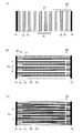
- a configuration in which the first piezoelectric ceramics 18 and the second piezoelectric ceramics 20 that are formed in a shape are alternately stacked may be employed.
- the composite ceramic 52 has a configuration in which the first piezoelectric ceramics 18 and the second piezoelectric ceramics 20 are alternately stacked in the polarization direction.
- the external electrodes 14 and 16 are formed in parallel with these ceramic layers.
- the piezoelectric drive element 50 is driven in the direction of arrow Fb.
- the piezoelectric driving element 60 in the example shown in FIG. 4B alternately stacks the first piezoelectric ceramic 18 layers and the second piezoelectric ceramic 20 layers in the direction orthogonal to the polarization direction. Along with these first and second piezoelectric ceramic layers, a plurality of internal electrodes 32 and 34 joined to the external electrodes 14 and 16 are alternately arranged in the same manner as in the second embodiment. Driven in the direction of arrow Fb.
- a piezoelectric drive element 70 shown in FIG. 4 (C) is a modification of the piezoelectric drive block 60 shown in FIG. 4 (B), and the composite ceramic 72 is composed of the first piezoelectric ceramic 18 and the second piezoelectric body.
- the internal electrodes 32 and 34 are formed between the laminated bodies of the ceramics 20.
- the piezoelectric drive element 70 is driven in the direction of arrow Fb.
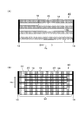
- the first piezoelectric ceramic 18 and the second piezoelectric ceramic 20 are laminated in the direction in which the electric field is applied.
- the composite ceramic 82 is different from the above-mentioned FIGS. 4 (A) to (C) in that the first piezoelectric ceramic 18 layer is arranged in the direction perpendicular to the applied electric field. And layers of the second piezoelectric ceramics 20 are alternately laminated.
- the piezoelectric driving element 80 is driven in the direction of arrow Fb.
- the piezoelectric drive element 90 shown in FIG. 5B is in a composite ceramic 92 in which the first piezoelectric ceramic 18 and the second piezoelectric ceramic 20 are laminated in the same direction as in FIG. 4A.
- the first piezoelectric ceramic 18 and the second piezoelectric ceramic 20 are stacked in the direction orthogonal to the applied electric field by forming the plurality of internal electrodes 32 and 34 so as to be orthogonal to the stacking direction of the ceramic layers. It has a configuration.
- Example 3 Next, a specific example of this example will be further described.
- a piezoelectric ceramic of (K 0.5 , Na 0.5 ) NbO 3 is selected
- the second piezoelectric ceramic 20 having a hard spring characteristic Sr 1.9 Ca O.S. 1 NaNb 5 O 15 piezoelectric ceramics were selected, and each piezoelectric ceramic powder was prepared and mixed in the same manner as in Experimental Example 1 of Example 1 described above.
- the mixed powder was mixed with an organic solvent and an organic binder to form a slurry, which was formed into a sheet by a doctor blade method.
- FIGS. 4 (A) to 4 (C) and FIG. 5 (A) are appropriately performed, and the piezoelectric drive having the laminated structure shown in FIGS. 4 (A) to 4 (C) and FIG. 5 (A) is performed. Elements 50, 60, 70, and 80 were formed.
- this invention is not limited to the Example mentioned above, A various change can be added in the range which does not deviate from the summary of this invention.
- the following are also included.
- (1) The shapes and dimensions shown in the first to third embodiments are examples, and may be appropriately changed as necessary. The same applies to the materials, and it is preferable to select the first piezoelectric ceramic 18 and the second piezoelectric ceramic 20 from the material group shown in the above embodiment. Various electrode materials may be used.
- the first piezoelectric ceramic 18 and the second piezoelectric ceramic 20 are each formed on a planar sheet and laminated, but this is also an example.
- the laminated structure includes various forms. For example, like the composite ceramic 102 of the piezoelectric drive element 100 shown in FIG.
- the sheet-like first piezoelectric ceramic 18 and the second piezoelectric ceramic 20 are stacked and formed into a spiral shape (or roll shape).
- a structure in which the external electrodes 14 and 16 are provided on the end surfaces may be employed.
- the outer shape of the composite ceramic 102 is formed in a substantially rectangular parallelepiped shape, it is convenient in terms of mounting.
- stacked in roll shape you may laminate
- the powder first piezoelectric ceramic 18 and the second piezoelectric ceramic 20 are mixed to form a composite form.
- the particle shape of the powder is indefinite, spherical, The shape can be changed as appropriate, such as a plate shape or a fiber shape.
- the number of laminations of the internal electrodes 32 and 34 shown in Examples 2 and 3 and the number of laminations of the first piezoelectric ceramic 18 and the second piezoelectric ceramic 20 shown in Example 3 are examples. The amount may be increased or decreased as appropriate to achieve the same effect.
- the method of manufacturing the piezoelectric driving element shown in the above embodiment is also an example, and may be appropriately changed so as to achieve the same effect.
- the piezoelectric drive elements of the various embodiments described above are preferably used as, for example, piezoelectric actuators, but other devices having various known drive units (for example, camera photographing lenses and overhead projectors). Applicable to piezoelectric drive devices generally used for devices with a drive unit such as projection lenses, binoculars lenses, copier lenses, etc., as well as driving lenses in optical devices, such as plotters and XY drive tables) Is possible.
- the piezoelectric drive elements of the various embodiments described above are particularly suitable for devices that require stable driving at the resonance frequency and frequencies in the vicinity thereof.
- Piezoelectric drive element 12 Composite ceramics 14, 16: External electrode 18: First piezoelectric ceramic 20: Second piezoelectric ceramic 30, 50, 60, 70, 80, 90, 100: Piezoelectric drive element 32, 34: Internal electrodes 52, 62, 72, 82, 92, 102: Composite ceramics 200: Resonant actuator 202: Piezoelectric ceramic body 204a, 204b: Electrodes 206a, 206b: Spring terminals 208a, 208b: Conductor 210: AC power supply 250: Resonant actuator 252: Piezoelectric ceramic body 254a, 254b: Electrodes 256a, 256b: Connection electrodes 258a, 258b: Lead conductors 260a, 260b: Spring terminals
Landscapes
- Engineering & Computer Science (AREA)
- Manufacturing & Machinery (AREA)
- Chemical & Material Sciences (AREA)
- Composite Materials (AREA)
- Materials Engineering (AREA)
- General Electrical Machinery Utilizing Piezoelectricity, Electrostriction Or Magnetostriction (AREA)
- Compositions Of Oxide Ceramics (AREA)
Abstract
Description
次に、本実施例の具体例について更に説明する。前記柔らかいばね特性を有する第1の圧電体セラミックス18として、(K0.5,Na0.5)NbO3の圧電体セラミックスを選定し、硬いばね特性を有する第2の圧電体セラミックス20として、Sr1.9CaO.1NaNb5O15の圧電体セラミックスを選定した。それぞれの圧電体セラミックスの粉体は、K2CO3,Na2CO3,Nb2O5,SrCO3,CaCO3を化学量論組成に秤量、混合後、仮焼する固相合成法により作製した。作製したそれぞれの圧電体セラミックスには、機械的品質係数を高めるために、Mn2Oを0.5wt%添加した。そして、これらの圧電体セラミックスの粉体を、それぞれ体積分率が同じになるように秤量、混合し、該混合物を1150℃でスパークプラズマ焼成して、大気中で900℃で熱処理し、複合セラミックスを作製した。
(1)前記実施例1~3で示した形状,寸法は一例であり、必要に応じて適宜変更してよい。材料についても同様であり、第1の圧電体セラミックス18及び第2の圧電体セラミックス20については前記実施例で示した材料群から選択することが好ましいが、内部電極や外部電極については、公知の各種の電極材料を利用してよい。
(2)前記実施例3では、第1の圧電体セラミックス18及び第2の圧電体セラミックス20を、それぞれ平面状のシートに形成して、それらを積層することとしたが、これも一例であり、積層構造には種々の形態が含まれる。例えば、図6に示す圧電駆動素子100の複合セラミックス102のように、シート状の第1の圧電体セラミックス18と第2の圧電体セラミックス20とを重ねて渦巻き状(ないしロール状)に成形したもの利用し、外部電極14,16を端面に設けた構成を採用してもよい。この場合、前記複合セラミックス102の外形が略直方体状となるように形成すると、実装面で都合がよい。また、図6の例では、ロール状に積層したが、同心円状に積層してもよい。
(4)前記実施例2及び3に示した内部電極32,34の積層数や、実施例3に示した第1の圧電体セラミックス18及び第2の圧電体セラミックス20の積層数も一例であり、同様の効果を奏するように適宜増減してよい。
(5)前記実施例で示した圧電駆動素子の製造方法も一例であり、同様の効果を奏するように適宜変更してよい。
(6)上述した様々な実施形態の圧電駆動素子は、例えば、圧電アクチュエータなどが好適な利用例であるが、他の公知の各種の駆動部を有する装置(例えば、カメラの撮影レンズやオーバーヘッドプロジェクタなどの投影レンズ,双眼鏡のレンズ,複写機のレンズなど、光学装置におけるレンズの駆動のほか、プロッタやX-Y駆動テーブルのような装置)など、駆動部を有する装置一般に用いる圧電駆動装置に適用可能である。上述した様々な実施形態の圧電駆動素子は、特に、共振周波数及びその近傍の周波数での安定した駆動が必要とされる装置に好適である。
12:複合セラミックス
14,16:外部電極
18:第1の圧電体セラミックス
20:第2の圧電体セラミックス
30,50,60,70,80,90,100:圧電駆動素子
32,34:内部電極
52,62,72,82,92,102:複合セラミックス
200:共振アクチュエータ
202:圧電セラミック素体
204a,204b:電極
206a,206b:ばね端子
208a,208b:導線
210:交流電源
250:共振アクチュエータ
252:圧電セラミック素体
254a,254b:電極
256a,256b:接続電極
258a,258b:引出導体
260a,260b:ばね端子
Claims (7)
- 振動速度が増加すると弾性定数が小さくなるばね特性を有する第1の圧電体セラミックスと、振動速度が増加すると弾性定数が大きくなるばね特性を有する第2の圧電体セラミックスとを複合した複合セラミックスと、
該複合セラミックスを介して対向するように、該複合セラミックスの側面に設けられた外部電極と、
を具備し、
前記外部電極に、共振周波数及び共振周波数近傍の交流電界を印加して駆動する圧電駆動素子。 - 前記複合セラミックスは、前記第1の圧電体セラミックスと前記第2の圧電体セラミックスとを混合した構成、又は、前記第1の圧電体セラミックスと前記第2の圧電体セラミックスとを層状に重ねた構成を有する、請求項1に記載の圧電駆動素子。
- 前記複合セラミックスが、前記第1の圧電体セラミックスと前記第2の圧電体セラミックスとを、平面状,ロール状,同心円状のいずれかの形態で層状に重ねた構成を有する、請求項2記載の圧電駆動素子。
- 前記複合セラミックスの内部に、前記対向する外部電極のそれぞれに接続する複数の内部電極を設けて積層構造化した、請求項1から請求項3のいずれかに記載の圧電駆動素子。
- 前記第1の圧電体セラミックスと前記第2の圧電体セラミックスとの体積分率によって、前記複合セラミックスの弾性定数を調整し、振動速度の変化に対する共振周波数の変動を抑制する、請求項1から請求項4のいずれかに記載の圧電駆動素子。
- 前記第1の圧電体セラミックスが、PZTからなる鉛系圧電体セラミックス、BaTiO3,(Ba1/2Na1/2)TiO3,(Ba1/2K1/2)TiO3、および{(K1-xNax)1-yLiy}(Nb1-z-wTazSbw)O3(0≦x≦1,0≦y≦0.2,0≦z≦0.4,0≦w≦0.2)、又はこれらの少なくとも2種類を含む固溶体セラミックスであり、前記第2の圧電体セラミックスが、Sr2-xCaxNaNb5O15(0≦x≦2),Sr2NaNb5O15,Ca2NaNb5O15,Sr2KNb5O15,Ba2LiNb5O15,Ba2NaNb5O15,Ba2KNb5O15,K3Li2Nb5O15,Ba2Bi1/3Nb5O15,Pb2NaNb5O15,Pb2KNb5O15,又はこれらの少なくとも2種類を含むタングステンブロンズ型の固溶体セラミックスである、請求項1から請求項5のいずれかに記載の圧電駆動素子。
- 請求項1から請求項6のいずれかに記載の圧電駆動素子を含む圧電駆動装置。
Priority Applications (2)
| Application Number | Priority Date | Filing Date | Title |
|---|---|---|---|
| US13/876,455 US9147828B2 (en) | 2011-05-25 | 2012-04-18 | Piezoelectric drive element and piezoelectric drive unit |
| CN201280002904.7A CN103119740B (zh) | 2011-05-25 | 2012-04-18 | 压电驱动元件和压电驱动装置 |
Applications Claiming Priority (2)
| Application Number | Priority Date | Filing Date | Title |
|---|---|---|---|
| JP2011117484A JP5427835B2 (ja) | 2011-05-25 | 2011-05-25 | 圧電駆動素子及び圧電駆動装置 |
| JP2011-117484 | 2011-05-25 |
Publications (1)
| Publication Number | Publication Date |
|---|---|
| WO2012160910A1 true WO2012160910A1 (ja) | 2012-11-29 |
Family
ID=47216994
Family Applications (1)
| Application Number | Title | Priority Date | Filing Date |
|---|---|---|---|
| PCT/JP2012/060409 Ceased WO2012160910A1 (ja) | 2011-05-25 | 2012-04-18 | 圧電駆動素子及び圧電駆動装置 |
Country Status (4)
| Country | Link |
|---|---|
| US (1) | US9147828B2 (ja) |
| JP (1) | JP5427835B2 (ja) |
| CN (1) | CN103119740B (ja) |
| WO (1) | WO2012160910A1 (ja) |
Families Citing this family (2)
| Publication number | Priority date | Publication date | Assignee | Title |
|---|---|---|---|---|
| US9614463B2 (en) * | 2014-02-10 | 2017-04-04 | Tdk Corporation | Piezoelectric device, piezoelectric actuator, hard disk drive, and inkjet printer apparatus |
| CN115643783B (zh) * | 2022-11-07 | 2023-07-25 | 中南大学 | 多层定向多孔压电复合材料及制备和压电能量收集器 |
Citations (3)
| Publication number | Priority date | Publication date | Assignee | Title |
|---|---|---|---|---|
| WO2007083475A1 (ja) * | 2006-01-17 | 2007-07-26 | Murata Manufacturing Co., Ltd. | 共振アクチュエータ |
| WO2008090758A1 (ja) * | 2007-01-24 | 2008-07-31 | Murata Manufacturing Co., Ltd. | 共振アクチュエータ |
| JP2010062174A (ja) * | 2008-09-01 | 2010-03-18 | Honda Motor Co Ltd | 圧電セラミック材料及びアクチュエータ |
Family Cites Families (10)
| Publication number | Priority date | Publication date | Assignee | Title |
|---|---|---|---|---|
| JP4432280B2 (ja) * | 2001-05-23 | 2010-03-17 | Tdk株式会社 | 圧電磁器 |
| JP4001362B2 (ja) * | 2002-01-31 | 2007-10-31 | Tdk株式会社 | 圧電磁器およびその製造方法 |
| JP4734823B2 (ja) * | 2003-06-11 | 2011-07-27 | 富士通株式会社 | 膜多層構造体及びこれを用いるアクチュエータ素子、容量素子、フィルタ素子 |
| DE102004002204A1 (de) * | 2004-01-15 | 2005-08-11 | Epcos Ag | Keramikmaterial |
| US7264744B2 (en) * | 2004-03-26 | 2007-09-04 | Tdk Corporation | Piezoelectric ceramic and piezoelectric device |
| JP4873327B2 (ja) * | 2005-06-03 | 2012-02-08 | 株式会社村田製作所 | 圧電素子 |
| JP4973931B2 (ja) | 2007-03-27 | 2012-07-11 | Tdk株式会社 | 圧電磁器組成物 |
| JP2009058378A (ja) * | 2007-08-31 | 2009-03-19 | Murata Mfg Co Ltd | 磁気センサ |
| JP2010222194A (ja) * | 2009-03-24 | 2010-10-07 | Denso Corp | 結晶配向セラミックス及び積層型圧電素子の製造方法 |
| KR101248797B1 (ko) * | 2010-09-30 | 2013-04-03 | 티디케이가부시기가이샤 | 압전 자기 및 이를 구비하는 압전 소자, 및 이러한 압전 소자를 구비하는 압전 디바이스 |
-
2011
- 2011-05-25 JP JP2011117484A patent/JP5427835B2/ja active Active
-
2012
- 2012-04-18 CN CN201280002904.7A patent/CN103119740B/zh active Active
- 2012-04-18 US US13/876,455 patent/US9147828B2/en active Active
- 2012-04-18 WO PCT/JP2012/060409 patent/WO2012160910A1/ja not_active Ceased
Patent Citations (3)
| Publication number | Priority date | Publication date | Assignee | Title |
|---|---|---|---|---|
| WO2007083475A1 (ja) * | 2006-01-17 | 2007-07-26 | Murata Manufacturing Co., Ltd. | 共振アクチュエータ |
| WO2008090758A1 (ja) * | 2007-01-24 | 2008-07-31 | Murata Manufacturing Co., Ltd. | 共振アクチュエータ |
| JP2010062174A (ja) * | 2008-09-01 | 2010-03-18 | Honda Motor Co Ltd | 圧電セラミック材料及びアクチュエータ |
Also Published As
| Publication number | Publication date |
|---|---|
| US20130207512A1 (en) | 2013-08-15 |
| CN103119740B (zh) | 2015-04-01 |
| JP2012248584A (ja) | 2012-12-13 |
| US9147828B2 (en) | 2015-09-29 |
| CN103119740A (zh) | 2013-05-22 |
| JP5427835B2 (ja) | 2014-02-26 |
Similar Documents
| Publication | Publication Date | Title |
|---|---|---|
| JP5361635B2 (ja) | 振動体 | |
| CN102473525B (zh) | 电容装置和谐振电路 | |
| JP5021452B2 (ja) | 圧電/電歪磁器組成物および圧電/電歪素子 | |
| KR100379203B1 (ko) | 압전 세라믹 조성물, 압전 공진기, 압전 변압기, 압전 액츄에이터 및 압전 적층 소결체의 제조방법 | |
| WO2012105187A1 (ja) | 静電容量変化型発電素子 | |
| KR20120077160A (ko) | 압전 액츄에이터용 세라믹 조성물, 그 제조방법 및 이를 이용하여 제조된 압전 액츄에이터 | |
| JP5427835B2 (ja) | 圧電駆動素子及び圧電駆動装置 | |
| JP2017157830A (ja) | 圧電磁器板および板状基体ならびに電子部品 | |
| WO2024070626A1 (ja) | 無鉛圧電組成物、及び圧電素子 | |
| KR100198162B1 (ko) | 압전 트랜스포머 | |
| WO2019172064A1 (ja) | 圧電アクチュエータ、及び、圧電アクチュエータの駆動方法 | |
| US10381544B2 (en) | System and fabrication method of piezoelectric stack that reduces driving voltage and clamping effect | |
| CN1284752A (zh) | 压电元件 | |
| JP2007013096A (ja) | 圧電アクチュエータおよびその駆動方法、並びに印刷ヘッド | |
| JPWO2013088927A1 (ja) | 圧電配向セラミックスおよび圧電アクチュエータ | |
| JP5482609B2 (ja) | 圧電磁器及びこれを備える圧電素子、並びにかかる圧電素子を備える圧電デバイス | |
| JP2025047156A (ja) | 圧電素子 | |
| WO2025191914A1 (ja) | 積層圧電セラミック素子及び装置 | |
| JP6321562B2 (ja) | 圧電磁器組成物、圧電素子および圧電振動装置 | |
| KR20250139807A (ko) | 적층 압전 세라믹 부품, 및 그것을 구비하는 장치 | |
| JP5935187B2 (ja) | 圧電セラミックスおよびこれを用いた圧電アクチュエータ | |
| WO2025047499A1 (ja) | 圧電素子 | |
| JPS63268279A (ja) | 圧電バイモルフ素子 | |
| JPH0349271A (ja) | 積層圧電セラミックス素子の製造方法 | |
| JP2020202338A (ja) | 圧電セラミックス |
Legal Events
| Date | Code | Title | Description |
|---|---|---|---|
| WWE | Wipo information: entry into national phase |
Ref document number: 201280002904.7 Country of ref document: CN |
|
| 121 | Ep: the epo has been informed by wipo that ep was designated in this application |
Ref document number: 12789144 Country of ref document: EP Kind code of ref document: A1 |
|
| WWE | Wipo information: entry into national phase |
Ref document number: 13876455 Country of ref document: US |
|
| NENP | Non-entry into the national phase |
Ref country code: DE |
|
| 122 | Ep: pct application non-entry in european phase |
Ref document number: 12789144 Country of ref document: EP Kind code of ref document: A1 |