WO2012160624A1 - 絶縁膜形成方法 - Google Patents
絶縁膜形成方法 Download PDFInfo
- Publication number
- WO2012160624A1 WO2012160624A1 PCT/JP2011/061656 JP2011061656W WO2012160624A1 WO 2012160624 A1 WO2012160624 A1 WO 2012160624A1 JP 2011061656 W JP2011061656 W JP 2011061656W WO 2012160624 A1 WO2012160624 A1 WO 2012160624A1
- Authority
- WO
- WIPO (PCT)
- Prior art keywords
- substrate
- insulating film
- heating
- ultraviolet irradiation
- forming method
- Prior art date
- Legal status (The legal status is an assumption and is not a legal conclusion. Google has not performed a legal analysis and makes no representation as to the accuracy of the status listed.)
- Ceased
Links
Images


Classifications
-
- H—ELECTRICITY
- H10—SEMICONDUCTOR DEVICES; ELECTRIC SOLID-STATE DEVICES NOT OTHERWISE PROVIDED FOR
- H10P—GENERIC PROCESSES OR APPARATUS FOR THE MANUFACTURE OR TREATMENT OF DEVICES COVERED BY CLASS H10
- H10P14/00—Formation of materials, e.g. in the shape of layers or pillars
- H10P14/60—Formation of materials, e.g. in the shape of layers or pillars of insulating materials
- H10P14/66—Formation of materials, e.g. in the shape of layers or pillars of insulating materials characterised by the type of materials
- H10P14/668—Formation of materials, e.g. in the shape of layers or pillars of insulating materials characterised by the type of materials the materials being characterised by the deposition precursor materials
- H10P14/6681—Formation of materials, e.g. in the shape of layers or pillars of insulating materials characterised by the type of materials the materials being characterised by the deposition precursor materials the precursor containing a compound comprising Si
- H10P14/6687—Formation of materials, e.g. in the shape of layers or pillars of insulating materials characterised by the type of materials the materials being characterised by the deposition precursor materials the precursor containing a compound comprising Si the compound comprising silicon and nitrogen
- H10P14/6689—Formation of materials, e.g. in the shape of layers or pillars of insulating materials characterised by the type of materials the materials being characterised by the deposition precursor materials the precursor containing a compound comprising Si the compound comprising silicon and nitrogen the compound being a silazane
-
- H—ELECTRICITY
- H10—SEMICONDUCTOR DEVICES; ELECTRIC SOLID-STATE DEVICES NOT OTHERWISE PROVIDED FOR
- H10P—GENERIC PROCESSES OR APPARATUS FOR THE MANUFACTURE OR TREATMENT OF DEVICES COVERED BY CLASS H10
- H10P14/00—Formation of materials, e.g. in the shape of layers or pillars
- H10P14/60—Formation of materials, e.g. in the shape of layers or pillars of insulating materials
- H10P14/63—Formation of materials, e.g. in the shape of layers or pillars of insulating materials characterised by the formation processes
- H10P14/6326—Deposition processes
- H10P14/6342—Liquid deposition, e.g. spin-coating, sol-gel techniques or spray coating
-
- H—ELECTRICITY
- H10—SEMICONDUCTOR DEVICES; ELECTRIC SOLID-STATE DEVICES NOT OTHERWISE PROVIDED FOR
- H10P—GENERIC PROCESSES OR APPARATUS FOR THE MANUFACTURE OR TREATMENT OF DEVICES COVERED BY CLASS H10
- H10P14/00—Formation of materials, e.g. in the shape of layers or pillars
- H10P14/60—Formation of materials, e.g. in the shape of layers or pillars of insulating materials
- H10P14/65—Formation of materials, e.g. in the shape of layers or pillars of insulating materials characterised by treatments performed before or after the formation of the materials
- H10P14/6516—Formation of materials, e.g. in the shape of layers or pillars of insulating materials characterised by treatments performed before or after the formation of the materials of treatments performed after formation of the materials
- H10P14/6536—Formation of materials, e.g. in the shape of layers or pillars of insulating materials characterised by treatments performed before or after the formation of the materials of treatments performed after formation of the materials by exposure to radiation, e.g. visible light
- H10P14/6538—Formation of materials, e.g. in the shape of layers or pillars of insulating materials characterised by treatments performed before or after the formation of the materials of treatments performed after formation of the materials by exposure to radiation, e.g. visible light by exposure to UV light
Definitions
- the present invention relates to an insulating film forming method for forming an insulating film on a substrate in a semiconductor device.
- a polymer insulating film such as polyvinylphenol is well known, but there are problems such as insufficient insulating properties and durability.
- SiO 2 used as a gate insulating film in a silicon transistor is known to be very stable and highly reliable.
- a semiconductor device capable of forming an insulating film on a substrate with a low insulating temperature and good insulating characteristics during heat treatment. It is an object of the present invention to provide a method for forming an insulating film.
- An insulating film forming method for a semiconductor device is a coating step of applying a catalyst-containing insulating material solution to a surface of a substrate; a heating step of performing a heat treatment on the substrate after the coating step; After the heating step, the substrate is further subjected to a heat treatment and an ultraviolet irradiation step of irradiating the surface of the substrate with ultraviolet rays to form an insulating film on the substrate.
- the substrate is subjected to heat treatment by heat treatment, and then irradiated with ultraviolet rays.
- the substrate is further heat-treated, and the substrate is irradiated with ultraviolet rays to form an insulating film on the substrate, so that the temperature of the heat treatment in each of the heating step and the ultraviolet ray irradiation step can be made lower than before.
- the insulating characteristics of an insulating film formed to a thickness of 100 nm or more can be improved.
- FIG. 1 shows an insulating film forming method of the present invention.
- the insulating film forming method of FIG. 1 is a method of forming a SiO 2 film.
- the insulating film forming method includes (a) a coating process, (b) a drying process, (c) a heating process, and (d) an ultraviolet irradiation process.
- the substrate 11 is placed on the turntable 12.
- the substrate 11 is made of a glass substrate or a plastic substrate (including a flexible substrate). The substrate 11 is rotated in a direction indicated by an arrow A in FIG.
- a Pd-based catalyst-containing polysilazane solution 13 (catalyst) is formed by spin coating.
- the containing insulating material solution) is applied to the surface of the substrate 11.
- the polysilazane solution 13 is dropped from a syringe 14 located above the rotating substrate 11, and thereby applied to the surface of the substrate 11.
- the reason for using the polysilazane solution 13 is that the conversion reactivity is high and the temperature of the heat treatment can be lowered.
- the hot plate 16 contacts the back surface of the substrate 11 and heats the substrate 11 containing the polysilazane solution 13 in the atmosphere.
- the treatment conditions in this drying step are drying by heating at a temperature of 50 ° C. for 10 minutes. This is executed by controlling the hot plate 16 under these conditions.
- the solvent of the polysilazane solution 13 is removed and a dry film is formed.
- bubbles can be prevented from being generated in the insulating film.
- the dry film 17 is heated by the hot plate 22 in the presence of oxygen in the irradiation chamber 21. Further, the ultraviolet ray 23 a is emitted from the ultraviolet irradiation unit 23 to the dry film 17.
- the treatment condition of this step is ultraviolet irradiation for 2 hours in a heating state at a temperature of 150 ° C.
- the above-described (a) coating step, (b) drying step, (c) heating step, and (d) ultraviolet irradiation step are performed, so The polysilazane solution 13 can be converted into a SiO 2 insulating film. Since the maximum heating temperature of each of the (b) drying step, (c) heating step, and (d) ultraviolet irradiation step is 150 ° C., a plastic substrate can be used as the substrate 11. In addition, since the oxygen content in the formed insulating film is about 40% as will be described later, good insulating characteristics can be obtained.
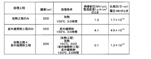
- FIG. 2 shows an actual measurement example of the withstand voltage and the specific resistance as the insulating characteristics of the insulating film in each case where the insulating film forming method is only the heating process, only the ultraviolet irradiation process, and heating process + ultraviolet irradiation process. .
- the film thickness is 200 nm and the heating temperature in each step is 150 ° C.
- the total processing time is 2 hours 30 minutes, but in the case of only the heating process of 3 hours or the same 3 hours of ultraviolet irradiation process Compared with the case of only the above, the withstand voltage and the specific resistance are 6.1 MV / cm and 1.3 ⁇ 10 15 ⁇ ⁇ cm, respectively, and good results are obtained.
- FIG. 3A shows the result of analyzing the insulating film formed only by the ultraviolet irradiation process by X-ray photoelectron spectroscopy (XPS), and FIG. 3B shows the XPS formed by the heating process + ultraviolet irradiation process.
- XPS X-ray photoelectron spectroscopy
- FIG. 3B shows the XPS formed by the heating process + ultraviolet irradiation process.
- the result of analysis is shown.
- 3 (a) and 3 (b) the oxygen (O) content in the insulating film formed only by the ultraviolet irradiation process is about 20%, and the inside of the insulating film formed by the heating process + ultraviolet irradiation process is about 20%. It can be seen that the oxygen (O) content is about 40%.
- the insulating film formed in the heating step + ultraviolet irradiation step of the insulating film forming method of the present invention has more oxygen (O) incorporated in the insulating film than the insulating film only in the ultraviolet irradiation step, A dense film can be formed. Therefore, when the insulating film using the insulating film forming method of the present invention is formed to have a film thickness of 100 nm or more, for example, the insulating characteristics are better as compared with the insulating film formed only by the ultraviolet irradiation process.
- the substrate 11 is directly heated from the back surface thereof by the hot plate 16 as a heating element. Therefore, the substrate is not disposed in the closed space by using the heating chamber. A sufficient amount of heat can be added.
- the drying process and the heating process are distinguished in the above-described embodiments, the drying process may be included in the heating process.
- the processing conditions of each process are examples, and the insulating film forming method of the present invention is not limited to this.
- the solution is not limited to the polysilazane described above, and other solutions such as siloxane can be used.
- the method of directly forming the insulating film on the substrate is shown.
- the insulating film is gated on the substrate so as to cover the gate electrode.
- the present invention can be applied to form an insulating film.
- an insulating film can be formed at a low temperature, and a dense film having good insulating properties can be formed. Therefore, it can be applied as a barrier film (moisture-proof film) for a flexible substrate. .
Landscapes
- Formation Of Insulating Films (AREA)
Abstract
触媒含有絶縁材溶液を基板の表面に塗布する塗布工程と、塗布工程後、基板に対して加熱処理を施す加熱工程と、加熱工程後、基板に対して更に加熱処理を施すと共に紫外線を基板の表面に照射して基板上に絶縁膜を形成する紫外線照射工程と、を含む絶縁膜形成方法。
Description
本発明は、半導体装置において基板上に絶縁膜を形成する絶縁膜形成方法に関する。
近年、トランジスタの製造において、大面積でかつ、低コスト化の観点から、塗布法でトランジスタを作る研究が盛んに行われており、特に塗布法で作製された有機トランジスタが報告されている。
塗布法で作製されているゲート絶縁膜としては、ポリビニルフェノールといったポリマー絶縁膜が良く知られているが、絶縁特性や耐久性が十分でないなどの課題がある。
一方、シリコンのトランジスタでゲート絶縁膜として用いられている、SiO2は非常に安定であり、信頼性が高いことが知られている。
このようなことから、SiO2を塗布法で成膜しようとする試みがなされている。例としては、ポリシラザンやポリシロキサンを加熱する方法が知られている。また、ポリシラザンを酸素存在下で、UV(紫外線)を照射し、SiO2に転化する方法も報告されている。
しかしながら、ポリシラザンやポリシロキサンを加熱してSiO2に転化する方法では、400~500℃の高温で処理しなければならず、また、低温化の手段として、触媒を添加したものを用いても、300℃程度の加熱が必要であり、有機トランジスタの特徴を最大限に生かすことができるプラスチック基板への応用が困難である。
一方、酸素存在下における紫外線照射については、膜厚が50nm程度の薄膜であればSiO2への完全転化は可能であるが、100nm以上の膜厚になると難しい。トランジスタのゲート絶縁膜に使用するためには、電極のカバレッジを考慮すると、150~200nm程度の膜厚は必要である。例として特許文献1では紫外線照射によるSiO2への光転化は200℃程度で行われるが、実際には表面から20nm程度しか、SiO2に転化されておらず、膜が厚くなるに従って膜中の酸素含有量が少なく(180nmで26.3at%)、そのため膜厚が厚くなるに従って絶縁特性、特に絶縁耐圧に低下していくという問題があった。
そこで、本発明が解決しようとする課題は、上記の欠点が一例として挙げられ、加熱処理時の低温化を図りかつ良好な絶縁特性を有する絶縁膜を基板上に形成することができる半導体装置の絶縁膜形成方法を提供することが本発明の目的である。
請求項1に係る発明の半導体装置の絶縁膜形成方法は、触媒含有絶縁材溶液を基板の表面に塗布する塗布工程と、前記塗布工程後、前記基板に対して加熱処理を施す加熱工程と、前記加熱工程後、前記基板に対して更に加熱処理を施すと共に紫外線を前記基板の表面に照射して前記基板上に絶縁膜を形成する紫外線照射工程と、を含むことを特徴としている。
請求項1に係る発明の絶縁膜形成方法によれば、塗布工程にて触媒含有絶縁材溶液を基板に対して塗布した後、加熱処理にて基板に対して加熱処理を施し、その後、紫外線照射工程にて基板に対して更に加熱処理を施すと共に紫外線を基板に照射して基板上に絶縁膜を形成するので、加熱工程及び紫外線照射工程各々の加熱処理の温度を従来より低くすることができ、また、例えば、100nm以上の膜厚に形成された絶縁膜の絶縁特性を向上させることができる。
以下、本発明の実施例を図面を参照しつつ詳細に説明する。
図1は本発明の絶縁膜形成方法を示している。図1の絶縁膜形成方法はSiO2膜を形成する方法である。絶縁膜形成方法は図1(a)~(d)に示すように(a)塗布工程、(b)乾燥工程、(c)加熱工程、及び(d)紫外線照射工程を有する。
(a)塗布工程
先ず、基板11が回転台12上に配置される。基板11はガラス基板又はプラスチック基板(フレキシブル基板を含む)からなる。基板11は回転台12が図示しない回転駆動手段により回転駆動されることにより例えば、図1(a)に符号Aで示す矢印方向に回転され、スピンコート法によりPd系触媒入りポリシラザン溶液13(触媒含有絶縁材溶液)がその基板11の表面に塗布される。ポリシラザン溶液13は回転する基板11の上方に位置するシリンジ14から滴下され、それにより基板11の表面に塗布される。ポリシラザン溶液13を用いた理由は転化反応性が高く、加熱処理の温度を低下させることができるためである。
(b)乾燥工程
塗布工程の終了後、表面にポリシラザン溶液13が塗布された基板11は加熱源(発熱体)のホットプレート16上に載置される。ホットプレート16は基板11の裏面に接触してポリシラザン溶液13を含む基板11を大気中で加熱する。この乾燥工程における処理条件は温度50℃で10分間の加熱による乾燥である。この条件でホットプレート16を制御することにより実行される。この乾燥工程によりポリシラザン溶液13の溶媒が取り除かれて乾燥膜が形成される。このように乾燥工程を含むことにより絶縁膜中に気泡が発生することを防止することができる。
(c)加熱工程
乾燥工程後のポリシラザン溶液13の乾燥膜17が基板11と共に更に大気中でホットプレート16上において加熱処理される。加熱工程における処理条件は温度150℃にて30分間の加熱である。この加熱条件でホットプレート16を制御することにより実行される。
(d)紫外線照射工程
加熱工程後の乾燥膜17への紫外線照射は照射室21内で実行される。照射室21においてはホットプレート22が備えられ、そのホットプレート22上に乾燥膜17を有する基板11が載置される。乾燥膜17の上方には光源としてエキシマランプを用いた紫外線照射部23が設けられている。紫外線照射部23は照射室21の外部に配置された制御部24によって制御される。また、照射室21に酸素を供給する酸素供給部25が備えられている。
(a)塗布工程
先ず、基板11が回転台12上に配置される。基板11はガラス基板又はプラスチック基板(フレキシブル基板を含む)からなる。基板11は回転台12が図示しない回転駆動手段により回転駆動されることにより例えば、図1(a)に符号Aで示す矢印方向に回転され、スピンコート法によりPd系触媒入りポリシラザン溶液13(触媒含有絶縁材溶液)がその基板11の表面に塗布される。ポリシラザン溶液13は回転する基板11の上方に位置するシリンジ14から滴下され、それにより基板11の表面に塗布される。ポリシラザン溶液13を用いた理由は転化反応性が高く、加熱処理の温度を低下させることができるためである。
(b)乾燥工程
塗布工程の終了後、表面にポリシラザン溶液13が塗布された基板11は加熱源(発熱体)のホットプレート16上に載置される。ホットプレート16は基板11の裏面に接触してポリシラザン溶液13を含む基板11を大気中で加熱する。この乾燥工程における処理条件は温度50℃で10分間の加熱による乾燥である。この条件でホットプレート16を制御することにより実行される。この乾燥工程によりポリシラザン溶液13の溶媒が取り除かれて乾燥膜が形成される。このように乾燥工程を含むことにより絶縁膜中に気泡が発生することを防止することができる。
(c)加熱工程
乾燥工程後のポリシラザン溶液13の乾燥膜17が基板11と共に更に大気中でホットプレート16上において加熱処理される。加熱工程における処理条件は温度150℃にて30分間の加熱である。この加熱条件でホットプレート16を制御することにより実行される。
(d)紫外線照射工程
加熱工程後の乾燥膜17への紫外線照射は照射室21内で実行される。照射室21においてはホットプレート22が備えられ、そのホットプレート22上に乾燥膜17を有する基板11が載置される。乾燥膜17の上方には光源としてエキシマランプを用いた紫外線照射部23が設けられている。紫外線照射部23は照射室21の外部に配置された制御部24によって制御される。また、照射室21に酸素を供給する酸素供給部25が備えられている。
乾燥膜17は照射室21内において酸素存在下でホットプレート22によって加熱処理される。また、紫外線照射部23から紫外線23aが乾燥膜17に照射される。この工程の処理条件は温度150℃で加熱の状態で2時間の紫外線照射である。
このように、本発明の絶縁膜形成方法においては、上記の(a)塗布工程、(b)乾燥工程、(c)加熱工程、及び(d)紫外線照射工程を実行することにより、基板11上のポリシラザン溶液13をSiO2の絶縁膜に転化することができる。(b)乾燥工程、(c)加熱工程、及び(d)紫外線照射工程各々の最高加熱温度は150℃であるので、基板11としてプラスチック基板を用いることが可能となる。また、形成された絶縁膜中の酸素含有量が後述するように40%程度となるので、良好な絶縁特性を得ることができる。
図2は、絶縁膜形成方法が加熱工程のみの場合、紫外線照射工程のみの場合、加熱工程+紫外線照射工程の場合各々における絶縁膜の絶縁特性として絶縁耐圧及び比抵抗の実測例を示している。なお、膜厚は200nmで各工程での加熱温度は150℃である。この絶縁特性から分かるように、加熱工程+紫外線照射工程の場合には、工程合計の処理時間は2時間30分でありながら、3時間の加熱工程のみの場合、或いは同じ3時間の紫外線照射工程のみの場合と比較して、絶縁耐圧及び比抵抗が各々6.1MV/cm及び1.3×1015Ω・cmとなっており、良好な結果が得られている。
図3(a)は紫外線照射工程のみで形成された絶縁膜をX線光電子分光分析法(XPS)で分析した結果を示し、図3(b)は加熱工程+紫外線照射工程で形成されたXPSで分析した結果を示している。この図3(a),(b)から紫外線照射工程のみで形成された絶縁膜内部の酸素(O)含有率は20%程度であり、加熱工程+紫外線照射工程で形成された絶縁膜内部の酸素(O)含有率は40%程度であることが分かる。すなわち、本発明の絶縁膜形成方法の加熱工程+紫外線照射工程で形成された絶縁膜は紫外線照射工程のみの絶縁膜と比較して、絶縁膜中に酸素(O)が多く取り込まれており、緻密な膜ができる。よって、本発明の絶縁膜形成方法を用いた絶縁膜は、例えば、100nm以上の膜厚に形成する場合に、紫外線照射工程のみで形成された絶縁膜と比較して絶縁特性が良好となる。
上記の加熱工程及び乾燥工程においては、発熱体としてのホットプレート16により基板11がその裏面から直接加熱されるので、加熱チャンバーを使用して基板を閉塞空間に配置しなくても基板に対して十分な熱量を付加することができる。また、上記した実施例においては乾燥工程と加熱工程とを区別しているが、乾燥工程は加熱工程に含まれても良い。
なお、上記した実施例においては、各工程の処理条件は一例であり、本発明の絶縁膜形成方法はこれに限定されない。また、本発明では溶液としては上記したポリシラザンに限らず、シロキサン等の他の溶液を用いることができる。
また、上記した実施例では基板上に絶縁膜を直接形成する方法を示したが、フレキシブル基板等の基板上にゲート電極を形成した後、そのゲート電極を覆うように基板上に絶縁膜をゲート絶縁膜として形成するために本発明を適用することができる。更に、上記したように、低温で絶縁膜を形成することができ、かつ絶縁特性が良い緻密な膜を形成することができるので、フレキシブル基板用のバリア膜(防湿膜)としても応用可能である。
Claims (6)
- 触媒含有絶縁材溶液を基板の表面に塗布する塗布工程と、
前記塗布工程後、前記基板に対して加熱処理を施す加熱工程と、
前記加熱工程後、前記基板に対して更に加熱処理を施すと共に紫外線を前記基板の表面に照射して前記基板上に絶縁膜を形成する紫外線照射工程と、を含むことを特徴とする半導体装置の絶縁膜形成方法。 - 前記加熱工程の前に、前記加熱工程の加熱温度より低い温度で、前記基板に対して加熱処理する乾燥工程を更に含むことを特徴とする請求項1記載の絶縁膜形成方法。
- 前記絶縁材溶液は、ポリシラザンであることを特徴とする請求項1又は2記載の絶縁膜形成方法。
- 前記加熱工程の加熱時間は、前記紫外線照射工程の照射時間より短いことを特徴とする請求項1又は2記載の絶縁膜形成方法。
- 前記加熱工程及び前記乾燥工程は前記基板の裏面から加熱することを特徴とする請求項2記載の絶縁膜形成方法。
- 前記加熱工程及び前記乾燥工程は前記基板の裏面に発熱体を接触せしめる工程を含むことを特徴とする請求項5記載の絶縁膜形成方法。
Priority Applications (1)
| Application Number | Priority Date | Filing Date | Title |
|---|---|---|---|
| PCT/JP2011/061656 WO2012160624A1 (ja) | 2011-05-20 | 2011-05-20 | 絶縁膜形成方法 |
Applications Claiming Priority (1)
| Application Number | Priority Date | Filing Date | Title |
|---|---|---|---|
| PCT/JP2011/061656 WO2012160624A1 (ja) | 2011-05-20 | 2011-05-20 | 絶縁膜形成方法 |
Publications (1)
| Publication Number | Publication Date |
|---|---|
| WO2012160624A1 true WO2012160624A1 (ja) | 2012-11-29 |
Family
ID=47216730
Family Applications (1)
| Application Number | Title | Priority Date | Filing Date |
|---|---|---|---|
| PCT/JP2011/061656 Ceased WO2012160624A1 (ja) | 2011-05-20 | 2011-05-20 | 絶縁膜形成方法 |
Country Status (1)
| Country | Link |
|---|---|
| WO (1) | WO2012160624A1 (ja) |
Cited By (1)
| Publication number | Priority date | Publication date | Assignee | Title |
|---|---|---|---|---|
| CN112521647A (zh) * | 2020-12-23 | 2021-03-19 | 天津大学 | 基于光催化氧化表面接枝的聚丙烯薄膜绝缘特性提升方法 |
Citations (4)
| Publication number | Priority date | Publication date | Assignee | Title |
|---|---|---|---|---|
| JP2002072504A (ja) * | 2000-09-05 | 2002-03-12 | Clariant (Japan) Kk | 感光性ポリシラザン塗膜の焼成方法 |
| JP2002222691A (ja) * | 2000-07-24 | 2002-08-09 | Tdk Corp | 発光素子 |
| JP2011009619A (ja) * | 2009-06-29 | 2011-01-13 | Konica Minolta Holdings Inc | 薄膜トランジスタの製造方法及び薄膜トランジスタ |
| WO2011007543A1 (ja) * | 2009-07-17 | 2011-01-20 | 三井化学株式会社 | 積層体およびその製造方法 |
-
2011
- 2011-05-20 WO PCT/JP2011/061656 patent/WO2012160624A1/ja not_active Ceased
Patent Citations (4)
| Publication number | Priority date | Publication date | Assignee | Title |
|---|---|---|---|---|
| JP2002222691A (ja) * | 2000-07-24 | 2002-08-09 | Tdk Corp | 発光素子 |
| JP2002072504A (ja) * | 2000-09-05 | 2002-03-12 | Clariant (Japan) Kk | 感光性ポリシラザン塗膜の焼成方法 |
| JP2011009619A (ja) * | 2009-06-29 | 2011-01-13 | Konica Minolta Holdings Inc | 薄膜トランジスタの製造方法及び薄膜トランジスタ |
| WO2011007543A1 (ja) * | 2009-07-17 | 2011-01-20 | 三井化学株式会社 | 積層体およびその製造方法 |
Cited By (1)
| Publication number | Priority date | Publication date | Assignee | Title |
|---|---|---|---|---|
| CN112521647A (zh) * | 2020-12-23 | 2021-03-19 | 天津大学 | 基于光催化氧化表面接枝的聚丙烯薄膜绝缘特性提升方法 |
Similar Documents
| Publication | Publication Date | Title |
|---|---|---|
| Branquinho et al. | Aqueous combustion synthesis of aluminum oxide thin films and application as gate dielectric in GZTO solution-based TFTs | |
| Liu et al. | Enabling gate dielectric design for all solution-processed, high-performance, flexible organic thin-film transistors | |
| Tetzner et al. | Photonic curing of sol–gel derived HfO2 dielectrics for organic field-effect transistors | |
| Lin et al. | Deep ultraviolet laser direct write for patterning sol-gel InGaZnO semiconducting micro/nanowires and improving field-effect mobility | |
| US8557642B2 (en) | Method for providing lateral thermal processing of thin films on low-temperature substrates | |
| CN103066004B (zh) | 一种表面处理方法 | |
| JP2009545883A5 (ja) | ||
| CN103733319B (zh) | 晶体管的制造方法及晶体管 | |
| Han et al. | Optical and electrical analysis of annealing temperature of high-molecular weight hole transport layer for quantum-dot light-emitting diodes | |
| CN109256475A (zh) | 一种基于紫外热退火工艺的钙钛矿发光二极管及制备方法 | |
| Park et al. | Facile Polydimethylsiloxane Treatment of Indium Gallium Zinc Oxide Phototransistor for Visible Light‐Based Multilevel Photomemory | |
| WO2012160624A1 (ja) | 絶縁膜形成方法 | |
| Hashimoto et al. | Subsurface investigation of the surface modification of polydimethylsiloxane by 172‐nm vacuum ultraviolet irradiation using ToF‐SIMS and VUV spectrometry | |
| US7695998B2 (en) | Methods for making and using high-mobility inorganic semiconductive films | |
| US10128126B2 (en) | Method of doping 2-dimensional semiconductor | |
| Choi et al. | Flexible phototransistors integrated with chiral liquid crystal encapsulating film for improving color selectivity and stability | |
| Lin et al. | Electrical and surface properties of SiO2 films modified by ultraviolet irradiation and used as gate dielectrics for pentacene thin-film transistor applications | |
| Lee et al. | Molecular Engineering of Coordination Ligand for Multifunctional Sol–Gel Oxides | |
| CN103834188A (zh) | 光交联聚合物-有机硅氧烷混合胶柔性衬底及用于制备有机电子器件 | |
| WO2013176247A1 (ja) | トランジスタの製造方法およびトランジスタ | |
| Ambrosio et al. | Organic–inorganic hybrid thin films based in HfO2 nanoparticles as dielectric for flexible electronics | |
| KR102177459B1 (ko) | 폴리디메틸실록산을 이용한 비휘발성 멀티레벨 광 메모리 및 그 제조방법 | |
| JP5487522B2 (ja) | 酸化膜改質方法及び酸化膜改質装置 | |
| Abed et al. | Impacts of Device Geometry and Layout on Temperature Profile during Large‐Area Photonic Curing | |
| JPS62166529A (ja) | 薄膜の形成方法 |
Legal Events
| Date | Code | Title | Description |
|---|---|---|---|
| 121 | Ep: the epo has been informed by wipo that ep was designated in this application |
Ref document number: 11866225 Country of ref document: EP Kind code of ref document: A1 |
|
| NENP | Non-entry into the national phase |
Ref country code: DE |
|
| 122 | Ep: pct application non-entry in european phase |
Ref document number: 11866225 Country of ref document: EP Kind code of ref document: A1 |
|
| NENP | Non-entry into the national phase |
Ref country code: JP |