WO2012160616A1 - 表示装置 - Google Patents
表示装置 Download PDFInfo
- Publication number
- WO2012160616A1 WO2012160616A1 PCT/JP2011/006278 JP2011006278W WO2012160616A1 WO 2012160616 A1 WO2012160616 A1 WO 2012160616A1 JP 2011006278 W JP2011006278 W JP 2011006278W WO 2012160616 A1 WO2012160616 A1 WO 2012160616A1
- Authority
- WO
- WIPO (PCT)
- Prior art keywords
- common
- electrodes
- segment
- driver
- display panel
- Prior art date
- Legal status (The legal status is an assumption and is not a legal conclusion. Google has not performed a legal analysis and makes no representation as to the accuracy of the status listed.)
- Ceased
Links
Images

Classifications
-
- G—PHYSICS
- G02—OPTICS
- G02F—OPTICAL DEVICES OR ARRANGEMENTS FOR THE CONTROL OF LIGHT BY MODIFICATION OF THE OPTICAL PROPERTIES OF THE MEDIA OF THE ELEMENTS INVOLVED THEREIN; NON-LINEAR OPTICS; FREQUENCY-CHANGING OF LIGHT; OPTICAL LOGIC ELEMENTS; OPTICAL ANALOGUE/DIGITAL CONVERTERS
- G02F1/00—Devices or arrangements for the control of the intensity, colour, phase, polarisation or direction of light arriving from an independent light source, e.g. switching, gating or modulating; Non-linear optics
- G02F1/01—Devices or arrangements for the control of the intensity, colour, phase, polarisation or direction of light arriving from an independent light source, e.g. switching, gating or modulating; Non-linear optics for the control of the intensity, phase, polarisation or colour
- G02F1/13—Devices or arrangements for the control of the intensity, colour, phase, polarisation or direction of light arriving from an independent light source, e.g. switching, gating or modulating; Non-linear optics for the control of the intensity, phase, polarisation or colour based on liquid crystals, e.g. single liquid crystal display cells
- G02F1/133—Constructional arrangements; Operation of liquid crystal cells; Circuit arrangements
- G02F1/13306—Circuit arrangements or driving methods for the control of single liquid crystal cells
-
- G—PHYSICS
- G09—EDUCATION; CRYPTOGRAPHY; DISPLAY; ADVERTISING; SEALS
- G09G—ARRANGEMENTS OR CIRCUITS FOR CONTROL OF INDICATING DEVICES USING STATIC MEANS TO PRESENT VARIABLE INFORMATION
- G09G3/00—Control arrangements or circuits, of interest only in connection with visual indicators other than cathode-ray tubes
- G09G3/20—Control arrangements or circuits, of interest only in connection with visual indicators other than cathode-ray tubes for presentation of an assembly of a number of characters, e.g. a page, by composing the assembly by combination of individual elements arranged in a matrix no fixed position being assigned to or needed to be assigned to the individual characters or partial characters
- G09G3/34—Control arrangements or circuits, of interest only in connection with visual indicators other than cathode-ray tubes for presentation of an assembly of a number of characters, e.g. a page, by composing the assembly by combination of individual elements arranged in a matrix no fixed position being assigned to or needed to be assigned to the individual characters or partial characters by control of light from an independent source
- G09G3/36—Control arrangements or circuits, of interest only in connection with visual indicators other than cathode-ray tubes for presentation of an assembly of a number of characters, e.g. a page, by composing the assembly by combination of individual elements arranged in a matrix no fixed position being assigned to or needed to be assigned to the individual characters or partial characters by control of light from an independent source using liquid crystals
- G09G3/3611—Control of matrices with row and column drivers
- G09G3/3622—Control of matrices with row and column drivers using a passive matrix
- G09G3/3644—Control of matrices with row and column drivers using a passive matrix with the matrix divided into sections
-
- G—PHYSICS
- G09—EDUCATION; CRYPTOGRAPHY; DISPLAY; ADVERTISING; SEALS
- G09G—ARRANGEMENTS OR CIRCUITS FOR CONTROL OF INDICATING DEVICES USING STATIC MEANS TO PRESENT VARIABLE INFORMATION
- G09G3/00—Control arrangements or circuits, of interest only in connection with visual indicators other than cathode-ray tubes
- G09G3/04—Control arrangements or circuits, of interest only in connection with visual indicators other than cathode-ray tubes for presentation of a single character by selection from a plurality of characters, or by composing the character by combination of individual elements, e.g. segments using a combination of such display devices for composing words, rows or the like, in a frame with fixed character positions
-
- G—PHYSICS
- G09—EDUCATION; CRYPTOGRAPHY; DISPLAY; ADVERTISING; SEALS
- G09G—ARRANGEMENTS OR CIRCUITS FOR CONTROL OF INDICATING DEVICES USING STATIC MEANS TO PRESENT VARIABLE INFORMATION
- G09G3/00—Control arrangements or circuits, of interest only in connection with visual indicators other than cathode-ray tubes
- G09G3/20—Control arrangements or circuits, of interest only in connection with visual indicators other than cathode-ray tubes for presentation of an assembly of a number of characters, e.g. a page, by composing the assembly by combination of individual elements arranged in a matrix no fixed position being assigned to or needed to be assigned to the individual characters or partial characters
- G09G3/34—Control arrangements or circuits, of interest only in connection with visual indicators other than cathode-ray tubes for presentation of an assembly of a number of characters, e.g. a page, by composing the assembly by combination of individual elements arranged in a matrix no fixed position being assigned to or needed to be assigned to the individual characters or partial characters by control of light from an independent source
- G09G3/36—Control arrangements or circuits, of interest only in connection with visual indicators other than cathode-ray tubes for presentation of an assembly of a number of characters, e.g. a page, by composing the assembly by combination of individual elements arranged in a matrix no fixed position being assigned to or needed to be assigned to the individual characters or partial characters by control of light from an independent source using liquid crystals
- G09G3/3611—Control of matrices with row and column drivers
- G09G3/3674—Details of drivers for scan electrodes
- G09G3/3681—Details of drivers for scan electrodes suitable for passive matrices only
-
- G—PHYSICS
- G09—EDUCATION; CRYPTOGRAPHY; DISPLAY; ADVERTISING; SEALS
- G09G—ARRANGEMENTS OR CIRCUITS FOR CONTROL OF INDICATING DEVICES USING STATIC MEANS TO PRESENT VARIABLE INFORMATION
- G09G2310/00—Command of the display device
- G09G2310/02—Addressing, scanning or driving the display screen or processing steps related thereto
- G09G2310/0202—Addressing of scan or signal lines
- G09G2310/0205—Simultaneous scanning of several lines in flat panels
- G09G2310/021—Double addressing, i.e. scanning two or more lines, e.g. lines 2 and 3; 4 and 5, at a time in a first field, followed by scanning two or more lines in another combination, e.g. lines 1 and 2; 3 and 4, in a second field
-
- G—PHYSICS
- G09—EDUCATION; CRYPTOGRAPHY; DISPLAY; ADVERTISING; SEALS
- G09G—ARRANGEMENTS OR CIRCUITS FOR CONTROL OF INDICATING DEVICES USING STATIC MEANS TO PRESENT VARIABLE INFORMATION
- G09G2320/00—Control of display operating conditions
- G09G2320/02—Improving the quality of display appearance
- G09G2320/0238—Improving the black level
Definitions
- the present invention relates to a display device realized by a liquid crystal display device or the like.
- FIG. 2 is a front view showing an example of such a display device 1.
- the display panel 2 of the display device 1 can display 13 digits (characters).
- one of the 13 digits (characters) is framed and indicated by a reference symbol S1.
- 5 ⁇ 7 dot pixels (segments) 3 arranged in a matrix are used for display of one digit (character).
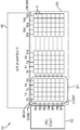
- FIG. 3 is a schematic wiring diagram of a display device 10 provided with a typical prior art drive circuit on a display panel 20 similar to the display panel 2 shown in FIG.
- the display panel 20 is formed in a longitudinal shape including a long side and a short side.
- the drive circuit includes a segment driver 40 disposed along the long side and a common driver 50 disposed along the short side.
- the display panel 20 displays the 13 digits (characters), and the pixel (segment) 3 of 5 ⁇ 7 dots is used to display 1 digit (characters), so that 65 segment electrodes SEG 1 to SEG 65 are used. , And seven common electrodes COM1 to COM7.
- the segment driver 40 controls the segment electrodes SEG1 to SEG65 from the terminals T1 to T65
- the common driver 50 individually controls the common electrodes COM1 to COM7 from the terminals P1 to P7.
- the display panel 20 is not a static drive display panel in which each pixel is driven individually, but has the segment electrodes SEG1 to SEG65 and the common electrodes COM1 to COM7, and the pixels at the intersections of these electrodes
- the display panel is a dynamic drive display panel in which a large number of pixels can be driven with a relatively small number of terminals by applying a drive voltage to each other and performing gray scale display.
- the display panel 20 is a simple display device that displays numbers, alphabets, and the like instead of an image etc. in the category of the display panel of the dynamic drive system, and elements and controls for storing charge in each pixel 3 It is a liquid crystal display panel of the simple (passive) matrix system which does not have the switch element for this.
- Patent Document 1 discloses a general liquid crystal panel drive system in a simple matrix liquid crystal display panel.
- the said drive system is an inversion drive system which prevents degradation of a liquid crystal panel by inverting the drive signal of a drive circuit with a fixed period.
- each pixel 3 performs different display.
- seven common electrodes COM1 to COM7 are sequentially selected, and each pixel 3 (segment) is driven at 1/7 duty. Therefore, in each pixel, the applied voltage decreases with the passage of time in the non-selection period.
- each pixel is always driven and there is no voltage drop.
- the display device of the dynamic drive system can drive many pixels with a relatively small number of terminals, the time for applying a voltage to each pixel 3 (segment) is shortened. For this reason, the above-described voltage drop tends to make the display contrast (brightness ratio between the ON segment and the OFF segment) and the viewing angle worse and the appearance (display quality) worse. Also, such a tendency becomes stronger as driving is performed at high duty and the number of terminals is reduced.
- An object of the present invention is to provide a display device that can improve display quality in a display device using a dynamic drive display panel.
- a display device includes one or a plurality of segment electrodes, a plurality of common electrodes, and a pixel arranged at the intersection of these electrodes, and a drive voltage is applied to the pixel to display And a first and a second segment driver for driving the segment electrode, and a first and a second common driver for driving the common electrode, wherein the common electrode is at least a first group and a second group.
- the common driver and the segment driver are provided corresponding to the first and second groups, respectively, and at least a part of a drive period of the first common driver and a drive period of the second common driver are provided. It is characterized by overlapping.
- FIG. 1 is a schematic wiring diagram of a display device provided with a typical prior art drive circuit.
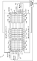
- FIG. 1 is a schematic wiring diagram of a display device 11 according to an embodiment of the present invention.
- the display device 11 includes a display panel 21 and its drive circuit.
- the drive circuit includes a driver group including a first segment driver 41, a second segment driver 42, a first common driver 51, and a second common driver 52, and a display control circuit 60 for controlling the driver group.
- the display panel 20 is formed in a longitudinal shape including a long side and a short side.
- the first segment driver 41 is disposed along one long side of the display panel 20, and the second segment driver 42 is disposed along the other long side.
- the first common driver 51 is disposed along one short side of the display panel 20, and the second common driver 42 is disposed along the other short side.
- the display panel 21 can display 13 digits (characters).
- a portion which is framed and indicated by reference numeral S1 is one segment for display of one digit (character). Therefore, the display panel 21 has 13 segments.
- the pixels 3 are disposed at intersections of segment electrodes SEG1 to SEG65 and common electrodes COM1 to COM7.
- a drive voltage is applied to the pixels 3 arranged at the intersections, and by performing display of gradation, dynamic drive can drive many pixels 3 with a relatively small number of terminals. It is a display panel of the method.
- the display panel 21 is a simple display device that displays numbers, alphabets, and the like instead of an image or the like in the display panel category of the dynamic drive system. Therefore, the display panel 21 is a liquid crystal display panel of a simple (passive) matrix type which does not have an element for storing charge and a switch element for control in each pixel 3.
- the seven common electrodes COM1 to COM7 are divided into two groups of four common electrodes COM1 to COM4 and three common electrodes COM5 to COM7.
- the former group is driven by the first common driver 51
- the latter group is driven by the second common driver 52.
- the common electrodes COM1 to COM4 are alternatively driven by the terminals P1-1 to P1-4 of the first common driver 51
- the common electrodes COM5 to COM7 are terminals of the second common driver 52 It is alternatively driven by P2-3.
- the 65 segment electrodes SEG1 to SEG65 are divided into two, upper and lower, with the boundary between the common electrodes COM4 and COM5 as a boundary.
- the upper segment electrodes SEG1 to SEG65 are driven by the first segment driver 41, and the lower ones are driven by the second segment driver 42.
- the common electrodes COM1 to COM4 of the segment electrodes SEG1 to SEG65 are simultaneously (simultaneously) driven by the terminals T1-1 to T1-65 of the first segment driver 41, and the common electrodes COM5 of the segment electrodes SEG1 to SEG65
- the terminals COM1 to COM7 are simultaneously (simultaneously) driven by the terminals T2-1 to T2-65 of the second segment driver 42.
- the first and second common drivers 51 and 52 perform driving at 1 ⁇ 4 duty of the unit drive cycle T.
- the common electrodes COM1 to COM3 and the common electrodes COM5 to COM7 are sequentially driven with a time shift of T / 4 from the start timing of the unit drive cycle T.
- only the common electrode COM4 is driven alone during the last T / 4 of the unit drive cycle T. That is, the common electrodes COM1 and COM5 are first driven at the start timing of the period T, the common electrodes COM2 and COM6 are driven after T / 4 elapses from the start timing, and the common electrodes COM3 and COM7 are driven after T / 4 elapses. After that, the common electrode COM4 is driven after T / 4.
- the display control circuit 60 generates a control signal corresponding to an image to be displayed on the display panel 21 and supplies the control signal to the first and second segment drivers 41 and 42 and the first and second common drivers 51 and 52.
- the control signals are a timing control signal for the above-mentioned simultaneous drive by the first and second segment drivers 41 and 42, and the above-mentioned 1/4 Duty by the first and second common drivers 51 and 52. And timing control signals for driving.
- the first and second common drivers 51 and 52 separately drive the plurality of common electrodes COM1 to COM7, and at least a part of the common electrodes (in the embodiment, the common electrodes COM1 to COM3 and the common electrodes COM5 to COM7)
- the duty can be raised by making it possible to drive simultaneously (in parallel).
- the viewing angle of the display panel 21 is widened, and the appearance (display quality) can be improved.
- the display panel 21 according to the present embodiment achieves a display quality as high as that of an LCD displaying a small amount of information formed of "symbol segments" while having an information amount of "5 ⁇ 7 dot segments". be able to.
- the common electrodes are driven at 1/7 duty.
- the driving can be performed at 1/4 Duty by the execution of the above-described simultaneous driving.
- the charging time for the pixel 3 can be extended from 1/7 of the unit driving cycle T to 1/4 of the period, that is, 75%.
- the display panel 21 is a simple simple (passive) matrix liquid crystal display panel as in the present embodiment
- the voltage applied to each pixel 3 decreases with the passage of time, so that the charging period can be extended. This is particularly effective for improving the display quality of the panel 21.
- the segment drivers can also be divided into two. Therefore, as in the present embodiment, the segment driver is divided into two of the first and second segment drivers 41 and 42, and these are arranged on the two opposing sides (long side in the above example) of the display panel 21. be able to. In the above example, the first and second common drivers 51 and 52 are disposed on the opposing short sides of the display panel 21 in the longitudinal shape, but may be disposed on the same short side. .
- the common electrodes COM1 to COM7 are driven at an equal 1 ⁇ 4 duty.
- the charging time may be further extended by driving at 1/3 duty.
- the common electrodes COM1 to COM7 are divided into two groups of four common electrodes COM1 to COM4 and three common electrodes COM5 to COM7.
- the common electrodes may be divided into three, two, two, or three or more groups.
- the case where seven common electrodes COM1 to COM7 are provided is illustrated.
- the number of common electrodes may be other than seven.
- the display panel 21 has a plurality of segments serving as display units, and a drive voltage is applied to one of the segments by m segment electrodes and n common electrodes.
- the n common electrodes are driven by the first common driver 51 and are driven by the second common driver 52 and the first group of n / 2 common electrodes and n / 2 or (n / 2).
- the display control circuit 60 drives the first common driver 51 to drive the first group of common electrodes, and the second common driver 52 drives the second group of common electrodes. It is desirable to make the timing of starting the same. As a result, the driving times of the common drivers 51 and 52 can be overlapped as much as possible, and there is an advantage that the charging time to the pixels 3 can be extended as much as possible.
- a display device includes one or a plurality of segment electrodes, a plurality of common electrodes, and a pixel arranged at the intersection of these electrodes, and a drive voltage is applied to the pixel to display And a first and a second segment driver for driving the segment electrode, and a first and a second common driver for driving the common electrode, wherein the common electrode is at least a first group and a second group.
- the common driver and the segment driver are provided corresponding to the first and second groups, respectively, and at least a part of a drive period of the first common driver and a drive period of the second common driver are provided. It is characterized by overlapping.
- the drive method can be improved.
- one or a plurality of signal wirings that is, column selection lines are driven simultaneously (simultaneously) by selection by the segment driver, and any common wiring is selected by selection by the common driver. That is, the row selection line is alternatively driven.
- the first and second groups of one or more common electrodes are combined, and the first and second common drivers and the first and second segments are provided correspondingly. Then, at least a part of both periods is overlapped in the driving periods of the first and second common drivers. That is, at least a part of the common electrodes can be driven simultaneously (in parallel) by driving the plurality of common electrodes by dividing the first and second common drivers.
- each common electrode has a period of T / N, that is, 1/1. It becomes possible to drive with N Duty.
- N Duty the time for applying a voltage to each pixel becomes longer, the contrast (brightness ratio between the ON segment and the OFF segment) can be improved, and the viewing angle becomes wider.
- the appearance can be improved.
- the display panel is preferably a liquid crystal display panel of a simple matrix.
- the common electrode is divided into only the first and second groups. According to this configuration, only two segment drivers are required, and it is not necessary to provide a plurality of segment electrodes in one pixel.
- the display panel has a plurality of segments serving as a display unit, one of the segments is composed of 5 ⁇ 7 dot pixels, and the common electrode is a first group of four common electrodes. Preferably, it is divided into a second group consisting of three common electrodes.
- the first and second common drivers drive each common electrode with equal 1/4 duty, and the common electrode of the first group and the common electrode of the second group are the same. Driving is started at a timing, and on the common electrode side of the second group, the driving period of one common electrode is blanked. Further, in the display device of the present invention, each common electrode is equal to one. It is desirable that driving is performed at 1/4 duty and that a driving period for one of the three groups of common electrodes is blanked.
- the three groups are driven at 1 ⁇ 3 duty, and the four groups are not driven at 1 ⁇ 4 duty, but both groups are driven at the same 1 ⁇ 4 duty. Therefore, since the duty is even, it is possible to eliminate the uneven brightness.
Landscapes
- Engineering & Computer Science (AREA)
- Physics & Mathematics (AREA)
- General Physics & Mathematics (AREA)
- Theoretical Computer Science (AREA)
- Computer Hardware Design (AREA)
- Crystallography & Structural Chemistry (AREA)
- Chemical & Material Sciences (AREA)
- Nonlinear Science (AREA)
- Mathematical Physics (AREA)
- Optics & Photonics (AREA)
- Control Of Indicators Other Than Cathode Ray Tubes (AREA)
- Liquid Crystal (AREA)
- Liquid Crystal Display Device Control (AREA)
Abstract
表示装置(11)は、1または複数のセグメント電極(SEG1~SEG65)と、複数のコモン電極(COM1~COM7)と、これらの電極の交点に配置された画素(3)とを有し、前記画素(3)に駆動電圧が印加され、表示を行う表示パネル(21)と、前記セグメント電極(SEG1~SEG65)を駆動する第1及び第2セグメントドライバ(41,42)と、前記コモン電極(COM1~COM7)を駆動する第1及び第2コモンドライバ(51,52)とを備える。前記コモン電極(COM1~COM7)は少なくとも第1及び第2グループに分割される。前記各コモンドライバ(51,52)およびセグメントドライバ(41,42)は、前記第1及び第2グループに対応してそれぞれ設けられる。前記第1コモンドライバ(51)の駆動期間と前記第2コモンドライバ(52)の駆動期間との少なくとも一部が重複している。
Description
本発明は、液晶表示装置などで実現される表示装置に関する。
従来から、ラジオの周波数表示や音楽の曲名表示などで、数字や英文字などを表示する簡単な表示装置が用いられている。図2は、このような表示装置1の一例を示す正面図である。この表示装置1の表示パネル2は、13桁(文字)の表示が可能である。図2では、13桁(文字)のうちの1桁(文字)分に枠掛けをし、参照符号S1で示している。この表示パネル2では、1桁(文字)分の表示に、マトリクス配列された5×7dotの画素(セグメント)3が用いられている。
図3は、図2に示す表示パネル2と同様な表示パネル20に、典型的な従来技術の駆動回路を具備した表示装置10の模式的な配線図である。前記13桁(文字)の表示のために、表示パネル20は、長辺と短辺とを備える長手形状に形成されている。前記駆動回路は、その長辺に沿って配置されたセグメントドライバ40と、短辺に沿って配置されたコモンドライバ50とを含む。表示パネル20は、前記13桁(文字)の表示を行い、1桁(文字)分の表示に5×7dotの画素(セグメント)3が使用されることから、65本のセグメント電極SEG1~SEG65と、7本のコモン電極COM1~COM7とを有する。セグメントドライバ40は、端子T1~T65から各セグメント電極SEG1~SEG65を、コモンドライバ50は、端子P1~P7から各コモン電極COM1~COM7を、それぞれ個別に制御する。
このように、表示パネル20は、各画素が個別に駆動されるスタティック駆動方式の表示パネルではなく、前記セグメント電極SEG1~SEG65とコモン電極COM1~COM7とを有し、それらの電極の交点における画素に駆動電圧が印加され、濃淡の表示を行うことで、多くの画素を比較的少ない端子数で駆動することができるダイナミック駆動方式の表示パネルである。また、表示パネル20は、そのダイナミック駆動方式の表示パネルのカテゴリの中でも、画像などではなく、数字や英文字などを表示する簡単な表示装置であり、各画素3において電荷を蓄積する要素や制御用のスイッチ素子を持たない単純(パッシブ)マトリクス方式の液晶表示パネルである。
特許文献1には、単純マトリクス方式の液晶表示パネルにおける一般的な液晶パネルの駆動方式が開示されている。当該駆動方式は、駆動回路の駆動信号を一定周期で反転させることで液晶パネルの劣化を防止する反転駆動方式である。
上記のダイナミック駆動方式の表示装置は、複数の画素3に共通のセグメント電極SEG1~SEG65およびコモン電極COM1~COM7を使用するが、各画素3(セグメント)はそれぞれ別の表示を行う。上述の5×7dotの例では、7本のコモン電極COM1~COM7が順次選択され、各画素3(セグメント)は1/7Dutyで駆動されることとなる。したがって、各画素では、非選択期間において、印加電圧が時間経過に伴い低下してゆく。一方、各画素に個別に端子を設けて各画素が個別に駆動されるスタティック駆動方式の表示パネルでは、各画素は常時駆動され、電圧低下は無い。
ダイナミック駆動方式の表示装置は、多くの画素を比較的少ない端子数で駆動することができるものの、各画素3(セグメント)に電圧を加える時間が短くなる。このため、上述の電圧低下によって、表示のコントラスト(ONしているセグメントとOFFしているセグメントとの輝度比)や、視野角が悪くなり、見映え(表示品位)が悪くなる傾向がある。また、そのような傾向は、高Dutyで駆動し、端子数を削減する程強くなる。
本発明の目的は、ダイナミック駆動方式の表示パネルを用いる表示装置において、表示品位を向上することができる表示装置を提供することにある。
本発明の一局面に係る表示装置は、1または複数のセグメント電極と、複数のコモン電極と、これらの電極の交点に配置された画素とを有し、前記画素に駆動電圧が印加され、表示を行う表示パネルと、前記セグメント電極を駆動する第1及び第2セグメントドライバと、前記コモン電極を駆動する第1及び第2コモンドライバと、を備え、前記コモン電極は少なくとも第1及び第2グループに分割され、前記各コモンドライバおよびセグメントドライバは前記第1及び第2グループに対応してそれぞれ設けられ、前記第1コモンドライバの駆動期間と前記第2コモンドライバの駆動期間との少なくとも一部が重複していることを特徴とする。
本発明の目的、特徴及び利点は、以下の詳細な説明と添付図面とによって、より明白となる。
図1は、本発明の実施形態に係る表示装置11の模式的な配線図である。表示装置11は、表示パネル21と、その駆動回路とを含む。該駆動回路は、第1セグメントドライバ41、第2セグメントドライバ42、第1コモンドライバ51及び第2コモンドライバ52からなるドライバ群と、このドライバ群を制御する表示制御回路60とを備える。表示パネル20は、長辺と短辺とを備える長手形状に形成されている。第1セグメントドライバ41は、表示パネル20の一方の長辺に沿って、第2セグメントドライバ42は他方の長辺に沿って配置されている。また、第1コモンドライバ51は、表示パネル20の一方の短辺に沿って、第2コモンドライバ42は他方の短辺に沿って配置されている。
表示パネル21は、13桁(文字)の表示が可能である。図1において枠掛けして参照符号S1で示す部分が、1桁(文字)分の表示のための1個のセグメントである。従って表示パネル21は、13個のセグメントを有している。1桁(文字)分の表示には、マトリクス配列された5×7dotの画素(セグメント)3が用いられる。したがって、この表示パネル21は、前述の表示パネル20と同様に、65本のセグメント電極SEG1~SEG65と、7本のコモン電極COM1~COM7とを有する。
前記画素3は、セグメント電極SEG1~SEG65とコモン電極COM1~COM7との各交点に配置されている。本実施形態の表示パネル21は、前記交点に配置された画素3に駆動電圧が印加され、濃淡の表示を行うことで、多くの画素3を比較的少ない端子数で駆動することができるダイナミック駆動方式の表示パネルである。また、表示パネル21は、ダイナミック駆動方式の表示パネルのカテゴリの中でも、画像などではなく、数字や英文字などを表示する簡単な表示装置である。従って、この表示パネル21は、各画素3において、電荷を蓄積する要素や制御用のスイッチ素子を持たない単純(パッシブ)マトリクス方式の液晶表示パネルである。
本実施形態においては、前記7本のコモン電極COM1~COM7が、4本のコモン電極COM1~COM4と、3本のコモン電極COM5~COM7との2つのグループに区分されている。前者のグループは、第1コモンドライバ51によって駆動され、後者のグループは第2コモンドライバ52によって駆動される。詳しくは、コモン電極COM1~COM4は、第1コモンドライバ51の端子P1-1~P1-4によって択一的に駆動され、コモン電極COM5~COM7は、第2コモンドライバ52の端子P2-1~P2-3によって択一的に駆動される。
これに対応して、前記65本のセグメント電極SEG1~SEG65は、コモン電極COM4とCOM5との間を境界として、上方と下方との2つに分断されている。上方のセグメント電極SEG1~SEG65は、第1セグメントドライバ41よって駆動され、下方のものは第2セグメントドライバ42によって駆動される。詳しくは、セグメント電極SEG1~SEG65のコモン電極COM1~COM4の側は、第1セグメントドライバ41の端子T1-1~T1-65によって一斉(同時)に駆動され、セグメント電極SEG1~SEG65のコモン電極COM5~COM7の側は、第2セグメントドライバ42の端子T2-1~T2-65によって一斉(同時)に駆動される。
第1、第2コモンドライバ51,52は、単位駆動周期Tの1/4Dutyでの駆動を行う。コモン電極COM1~COM3とコモン電極COM5~COM7とは、前記単位駆動周期Tの開始タイミングから、T/4の時間ずつずれて、順次駆動されてゆく。一方、コモン電極COM4だけが、前記単位駆動周期Tの最後のT/4の期間に、単独で駆動される。つまり、周期Tの開始タイミングにおいて先ずコモン電極COM1、COM5が駆動され、前記開始タイミングからT/4経過後にコモン電極COM2、COM6が駆動され、さらにT/4経過後にコモン電極COM3、COM7が駆動され、それから更にT/4経過後にコモン電極COM4が駆動される。
表示制御回路60は、表示パネル21において表示させる画像に対応した制御信号を生成し、第1、第2セグメントドライバ41,42及び第1、第2コモンドライバ51,52に前記制御信号を与える。具体的には前記制御信号は、第1、第2セグメントドライバ41,42による上述の一斉駆動のためのタイミング制御信号と、第1、第2コモンドライバ51,52による上述の1/4Dutyでの駆動のためのタイミング制御信号とを含む。
複数のコモン電極COM1~COM7を、第1及び第2コモンドライバ51,52が手分けして駆動し、少なくとも一部のコモン電極(本実施形態においてはコモン電極COM1~COM3とコモン電極COM5~COM7)を同時(並列)に駆動可能とすることで、Dutyを上げることができる。これによって、各画素3に電圧を加える時間を長くすることができ、コントラスト(ONしているセグメントとOFFしているセグメントとの輝度比)を向上させることができる。また、表示パネル21の視野角が広くなり、見映え(表示品位)を良くすることができる。たとえば、「5×7dotセグメント」の情報量を有しながら、「シンボルセグメント」で形成されている少量情報を表示しているLCD並みの高い表示品位を、本実施形態の表示パネル21では実現することができる。
具体的に上述の例のように、「5×7dotセグメント」の場合、コモン電極は7本必要となるので、従来技術によれば当該コモン電極は1/7Dutyで駆動されることとなる。しかしながら、7本のコモン電極COM1~COM7を、4本と3本との2つのグループに分けた場合、上述の同時駆動の実行によって1/4Dutyで駆動を行うことができる。これによって、画素3への充電時間を、前記単位駆動周期Tの1/7の期間から1/4の期間へ、すなわち75%も長くすることができる。本実施形態のように表示パネル21が、簡単な単純(パッシブ)マトリクスの液晶表示パネルの場合、各画素3の印加電圧は時間経過に伴い低下してゆくので、充電期間を長くできることは、表示パネル21の表示品位の向上のためには特に効果的である。
また、コモン電極COM1~COM7を2つのグループに分けた場合、セグメントドライバも2つに分けることができる。従って、本実施形態のように、セグメントドライバを第1、第2セグメントドライバ41,42の2つに分け、これらを表示パネル21の対向する2辺(上述の例では長辺)にそれぞれ配置することができる。なお、第1、第2コモンドライバ51,52は、上述の例では、長手形状の表示パネル21の対向する短辺にそれぞれ配置される例を示したが、同じ短辺に配置されてもよい。
上記実施形態では、前記各コモン電極COM1~COM7は、均等な1/4Dutyで駆動されている例を示した。これに代えて、3本のグループのコモン電極COM5~COM7側では、1/3Dutyで駆動されて、より充電時間を長くするようにしてもよい。しかしながら、表示パネル21の輝度ムラを無くすという観点からは、総てのコモン電極COM1~COM7においてDutyを均一にすることが好ましい。すなわち、Dutyを、上記実施形態のように2つのグループのうちの小さい方のDuty(1/4Duty)に合わせ、Dutyを大きくすることが可能なコモン電極COM5~COM7側では、1本のコモン電極分の駆動期間をブランクとして、全てのコモン電極COM1~COM7が均等なDutyで駆動されるようにすることが望ましい。
また、上記実施形態では、7本のコモン電極COM1~COM7が、4本のコモン電極COM1~COM4と、3本のコモン電極COM5~COM7との2つのグループに区分されている例を示した。しかし、コモン電極は、3本、2本、2本など、3つ以上のグループに区分されていてもよい。しかしながら、3つ又はそれ以上のグループに区分すると、長手形状の表示パネル21において、少なくとも一方の長辺側に複数のセグメントドライバを設ける必要が生じる。すなわち、短辺方向端部側に位置する画素(端子P1-1又は端子P2-3の行の画素)では、1つの画素に複数のセグメント電極が形成されることになる。この場合、本実施形態の単純(パッシブ)マトリクスの液晶表示パネルでは、クロストークが生じる可能性がある。このため、分割グループ数は、2が好適である。
さらに、上記実施形態では、7本のコモン電極COM1~COM7を備える場合を例示した。コモン電極は7本以外であっても良い。例えば、表示パネル21が、表示単位となるセグメントを複数有し、1つの前記セグメントはm本のセグメント電極とn本のコモン電極とによって駆動電圧が印加される場合を想定する。この場合、前記n個のコモン電極は、第1コモンドライバ51で駆動されn/2本のコモン電極からなる第1グループと、第2コモンドライバ52で駆動されn/2本又は(n/2-1)本のコモン電極からなる第2グループと、に分割することが望ましい。このようにコモン電極をグループに分割すれば、第1、第2コモンドライバ51、52の負担を略均等にすることができるので、制御バランスを良好にすることができる。
この場合、表示制御回路60が、第1コモンドライバ51が前記第1グループのコモン電極に対して駆動を開始するタイミングと、第2コモンドライバ52が前記第2グループのコモン電極に対して駆動を開始するタイミングとを同一にすることが望ましい。これにより、各コモンドライバ51、52の駆動時間を最大限に重複させることができ、画素3への充電時間を可及的に長くすることができる利点がある。
なお、上述した具体的実施形態には以下の構成を有する発明が主に含まれている。
本発明の一局面に係る表示装置は、1または複数のセグメント電極と、複数のコモン電極と、これらの電極の交点に配置された画素とを有し、前記画素に駆動電圧が印加され、表示を行う表示パネルと、前記セグメント電極を駆動する第1及び第2セグメントドライバと、前記コモン電極を駆動する第1及び第2コモンドライバと、を備え、前記コモン電極は少なくとも第1及び第2グループに分割され、前記各コモンドライバおよびセグメントドライバは前記第1及び第2グループに対応してそれぞれ設けられ、前記第1コモンドライバの駆動期間と前記第2コモンドライバの駆動期間との少なくとも一部が重複していることを特徴とする。
上記の構成によれば、ダイナミック駆動方式の表示パネルを用いる表示装置において、駆動方式を改善することができる。本発明の表示装置では、セグメントドライバが選択を行うことで、一斉(同時)に1または複数の信号配線、すなわち列選択線が駆動され、コモンドライバが選択を行うことで、任意の共通配線、すなわち行選択線が択一的に駆動される。ここで、前記コモン電極を1本または複数本纏めてなる第1及び第2グループとし、これに対応して第1及び第2コモンドライバと第1及び第2セグメントとを設けている。そして、第1及び第2コモンドライバの駆動期間において、少なくとも両期間の一部を重複させる。すなわち、複数のコモン電極を第1及び第2コモンドライバが手分けして駆動することで、少なくとも一部のコモン電極を同時(並列)に駆動可能とする。
したがって、たとえば単位駆動周期Tにおいて、最大のコモン電極を抱えるグループのコモンドライバが駆動するコモン電極の数をNとするとき、そのグループでは、各コモン電極は、T/Nの期間、すなわち1/NのDutyで駆動できるようになる。こうして、Dutyを上げることにより、各画素に電圧を加える時間が長くなり、コントラスト(ONしているセグメントとOFFしているセグメントとの輝度比)を向上することができるとともに、視野角が広くなり、見映え(表示品位)を良くすることができる。
上記表示装置において、前記表示パネルは、単純マトリクスの液晶表示パネルであることが望ましい。
簡単な単純(パッシブ)マトリクスの液晶表示パネルの場合、各画素の印加電圧は時間経過に伴い低下してゆく。このため、本発明が特に効果的である。
上記表示装置において、前記コモン電極は、第1及び第2グループにのみ分割されていることが望ましい。この構成によれば、セグメントドライバも2つで済み、1つの画素に複数のセグメント電極を設置しなくて済む。
上記表示装置において、前記表示パネルは、表示単位となるセグメントを複数有し、1つの前記セグメントは5×7dotの画素で構成され、前記コモン電極は、4本のコモン電極からなる第1グループと、3本のコモン電極からなる第2グループとに分割されていることが望ましい。
「5×7dotセグメント」の場合、コモン電極は7本必要となるので、通常は1/7Dutyでの駆動となってしまう。しかし、前記7本のコモン電極を2つのグループに分けて、第1コモンドライバは4本、第2コモンドライバは3本のコモン電極を駆動するので、1/4Dutyで駆動を行うことができる。これによって、画素への充電時間を、前記単位駆動周期Tの1/7の期間から1/4の期間へ、すなわち75%も長くすることができる。また、セグメントドライバも2つで済み、表示パネルの対向する2辺にそれぞれ設けることができる。
上記表示装置において、前記第1及び第2コモンドライバは、各コモン電極を均等な1/4Dutyで駆動するものであって、前記第1グループのコモン電極と前記第2グループのコモン電極とは同じタイミングで駆動が開始され、前記第2グループのコモン電極側では、1本のコモン電極分の駆動期間がブランクとされることまた、本発明の表示装置では、前記各コモン電極は、均等な1/4Dutyで駆動され、3本のグループのコモン電極側では、1本分の駆動期間がブランクとされることが望ましい。
上記の構成によれば、3本のグループが1/3Dutyで駆動され、4本のグループが1/4Dutyで駆動されるのではなく、両方のグループが同じ1/4Dutyで駆動される。したがって、Dutyが均等となるので、輝度ムラを無くすことができる。
Claims (7)
- 1または複数のセグメント電極と、複数のコモン電極と、これらの電極の交点に配置された画素とを有し、前記画素に駆動電圧が印加され、表示を行う表示パネルと、
前記セグメント電極を駆動する第1及び第2セグメントドライバと、
前記コモン電極を駆動する第1及び第2コモンドライバと、を備え、
前記コモン電極は少なくとも第1及び第2グループに分割され、
前記各コモンドライバおよびセグメントドライバは前記第1及び第2グループに対応してそれぞれ設けられ、
前記第1コモンドライバの駆動期間と前記第2コモンドライバの駆動期間との少なくとも一部が重複している、ことを特徴とする表示装置。 - 前記表示パネルは、単純マトリクスの液晶表示パネルであることを特徴とする請求項1記載の表示装置。
- 前記コモン電極は、第1及び第2グループにのみ分割されていることを特徴とする請求項2記載の表示装置。
- 前記表示パネルは、表示単位となるセグメントを複数有し、1つの前記セグメントは5×7dotの画素で構成され、
前記コモン電極は、4本のコモン電極からなる第1グループと、3本のコモン電極からなる第2グループとに分割されていることを特徴とする請求項2記載の表示装置。 - 前記第1及び第2コモンドライバは、各コモン電極を均等な1/4Dutyで駆動するものであって、前記第1グループのコモン電極と前記第2グループのコモン電極とは同じタイミングで駆動が開始され、
前記第2グループのコモン電極側では、1本のコモン電極分の駆動期間がブランクとされることを特徴とする請求項4記載の表示装置。 - 前記表示パネルは、表示単位となるセグメントを複数有し、1つの前記セグメントはm本のセグメント電極とn本のコモン電極とによって駆動電圧が印加され、
前記n個のコモン電極は、前記第1コモンドライバで駆動されn/2本のコモン電極からなる第1グループと、前記第2コモンドライバで駆動されn/2本又は(n/2-1)本のコモン電極からなる第2グループと、に分割されていることを特徴とする請求項2記載の表示装置。 - 前記第1コモンドライバが前記第1グループのコモン電極に対して駆動を開始するタイミングと、前記第2コモンドライバが前記第2グループのコモン電極に対して駆動を開始するタイミングとが実質的に同じである請求項6記載の表示装置。
Priority Applications (2)
| Application Number | Priority Date | Filing Date | Title |
|---|---|---|---|
| CN201180071094.6A CN103548075A (zh) | 2011-05-25 | 2011-11-09 | 显示装置 |
| US14/114,828 US20140063389A1 (en) | 2011-05-25 | 2011-11-09 | Display device |
Applications Claiming Priority (2)
| Application Number | Priority Date | Filing Date | Title |
|---|---|---|---|
| JP2011-117202 | 2011-05-25 | ||
| JP2011117202A JP2012247500A (ja) | 2011-05-25 | 2011-05-25 | 表示装置 |
Publications (1)
| Publication Number | Publication Date |
|---|---|
| WO2012160616A1 true WO2012160616A1 (ja) | 2012-11-29 |
Family
ID=47216723
Family Applications (1)
| Application Number | Title | Priority Date | Filing Date |
|---|---|---|---|
| PCT/JP2011/006278 Ceased WO2012160616A1 (ja) | 2011-05-25 | 2011-11-09 | 表示装置 |
Country Status (4)
| Country | Link |
|---|---|
| US (1) | US20140063389A1 (ja) |
| JP (1) | JP2012247500A (ja) |
| CN (1) | CN103548075A (ja) |
| WO (1) | WO2012160616A1 (ja) |
Families Citing this family (2)
| Publication number | Priority date | Publication date | Assignee | Title |
|---|---|---|---|---|
| CN103413538B (zh) * | 2013-08-27 | 2016-01-06 | 信利半导体有限公司 | 笔段式液晶显示器驱动电路及驱动方法 |
| TWI537904B (zh) * | 2014-12-18 | 2016-06-11 | 達意科技股份有限公司 | 顯示面板及其驅動方法 |
Citations (3)
| Publication number | Priority date | Publication date | Assignee | Title |
|---|---|---|---|---|
| JPS4934296A (ja) * | 1972-07-28 | 1974-03-29 | ||
| JPH0572996A (ja) * | 1991-09-13 | 1993-03-26 | Sharp Corp | 液晶表示体 |
| JP2002196727A (ja) * | 2000-12-27 | 2002-07-12 | Kyocera Corp | 液晶表示装置の駆動方法 |
Family Cites Families (17)
| Publication number | Priority date | Publication date | Assignee | Title |
|---|---|---|---|---|
| JPS6020074Y2 (ja) * | 1977-12-01 | 1985-06-15 | セイコーインスツルメンツ株式会社 | デイジタル表示式電子時計 |
| JPS5526592U (ja) * | 1978-08-11 | 1980-02-20 | ||
| JPS5577790A (en) * | 1978-12-08 | 1980-06-11 | Seiko Instr & Electronics | Multiplex liquid crystal display unit |
| JPS5859490A (ja) * | 1981-10-06 | 1983-04-08 | 株式会社東芝 | 表示制御装置 |
| JPS58184192A (ja) * | 1982-04-21 | 1983-10-27 | 株式会社精工舎 | ドツトマトリクス表示装置 |
| JPS59176985A (ja) * | 1983-03-26 | 1984-10-06 | Citizen Watch Co Ltd | 液晶テレビ受信装置 |
| JPS604991A (ja) * | 1983-06-23 | 1985-01-11 | 日本電気株式会社 | 螢光表示パネルおよびその駆動方法 |
| JPS62145291A (ja) * | 1985-12-20 | 1987-06-29 | カシオ計算機株式会社 | 液晶パネルの駆動方式 |
| JPS63185124U (ja) * | 1987-05-20 | 1988-11-29 | ||
| US5392058A (en) * | 1991-05-15 | 1995-02-21 | Sharp Kabushiki Kaisha | Display-integrated type tablet device |
| JP3253481B2 (ja) * | 1995-03-28 | 2002-02-04 | シャープ株式会社 | メモリインターフェイス回路 |
| JPH1138382A (ja) * | 1997-07-15 | 1999-02-12 | Alps Electric Co Ltd | 液晶表示装置 |
| JP2001249644A (ja) * | 2000-03-03 | 2001-09-14 | Kyocera Corp | 液晶表示装置 |
| JP2001356744A (ja) * | 2000-06-16 | 2001-12-26 | Sharp Corp | 液晶表示装置および携帯用電子機器 |
| JP2004077567A (ja) * | 2002-08-09 | 2004-03-11 | Semiconductor Energy Lab Co Ltd | 表示装置及びその駆動方法 |
| CN2632717Y (zh) * | 2003-07-09 | 2004-08-11 | 深圳市创欧科技有限公司 | 液晶显示装置 |
| JP2006039457A (ja) * | 2004-07-30 | 2006-02-09 | Oki Electric Ind Co Ltd | 表示パネルのスキャン方法及び表示装置 |
-
2011
- 2011-05-25 JP JP2011117202A patent/JP2012247500A/ja not_active Abandoned
- 2011-11-09 WO PCT/JP2011/006278 patent/WO2012160616A1/ja not_active Ceased
- 2011-11-09 CN CN201180071094.6A patent/CN103548075A/zh active Pending
- 2011-11-09 US US14/114,828 patent/US20140063389A1/en not_active Abandoned
Patent Citations (3)
| Publication number | Priority date | Publication date | Assignee | Title |
|---|---|---|---|---|
| JPS4934296A (ja) * | 1972-07-28 | 1974-03-29 | ||
| JPH0572996A (ja) * | 1991-09-13 | 1993-03-26 | Sharp Corp | 液晶表示体 |
| JP2002196727A (ja) * | 2000-12-27 | 2002-07-12 | Kyocera Corp | 液晶表示装置の駆動方法 |
Also Published As
| Publication number | Publication date |
|---|---|
| CN103548075A (zh) | 2014-01-29 |
| US20140063389A1 (en) | 2014-03-06 |
| JP2012247500A (ja) | 2012-12-13 |
Similar Documents
| Publication | Publication Date | Title |
|---|---|---|
| JP4880577B2 (ja) | 液晶ディスプレイ及びその表示方法 | |
| JP4551712B2 (ja) | ゲート線駆動回路 | |
| JP4953227B2 (ja) | ゲート駆動部を有する表示装置 | |
| EP2199850B1 (en) | Liquid crystal display with pixel pairs using a common gate line | |
| KR101385225B1 (ko) | 액정표시장치 및 그 구동방법 | |
| JP4419369B2 (ja) | 液晶表示装置及びその駆動方法 | |
| US8624812B2 (en) | Liquid crystal display | |
| CN101458904B (zh) | 显示装置 | |
| US9711098B2 (en) | Display apparatus with dummy pixel row and method of driving the display apparatus | |
| KR102237125B1 (ko) | 표시 장치 및 이의 구동 방법 | |
| CN1920932B (zh) | 显示装置及其驱动方法 | |
| KR20080099908A (ko) | 액정 표시 장치 및 그 구동 방법 | |
| US10347206B2 (en) | Drive circuit for display device and display device | |
| KR20090084665A (ko) | 멀티 도메인 디스플레이 디바이스 | |
| CN102419488A (zh) | 液晶显示装置及其驱动方法 | |
| US20100123702A1 (en) | Liquid crystal display and method of driving the same | |
| WO2013054724A1 (ja) | 表示装置およびその駆動方法 | |
| KR101857064B1 (ko) | 액정표시장치 | |
| KR20160096776A (ko) | 표시 장치 및 이의 구동방법 | |
| US8797244B2 (en) | Display device and method of driving the same | |
| KR101272177B1 (ko) | 액정표시장치의 회전 구동방법 | |
| WO2012160616A1 (ja) | 表示装置 | |
| CN101266745B (zh) | 一种显示装置及其驱动方法 | |
| US8982027B2 (en) | LCD drive circuit and driving method for scanning at least two adjacent scan lines simultaneously | |
| KR20060001331A (ko) | 액정표시장치의 구동방법 |
Legal Events
| Date | Code | Title | Description |
|---|---|---|---|
| 121 | Ep: the epo has been informed by wipo that ep was designated in this application |
Ref document number: 11866052 Country of ref document: EP Kind code of ref document: A1 |
|
| WWE | Wipo information: entry into national phase |
Ref document number: 14114828 Country of ref document: US |
|
| NENP | Non-entry into the national phase |
Ref country code: DE |
|
| 122 | Ep: pct application non-entry in european phase |
Ref document number: 11866052 Country of ref document: EP Kind code of ref document: A1 |