WO2012157722A1 - 液晶表示装置 - Google Patents
液晶表示装置 Download PDFInfo
- Publication number
- WO2012157722A1 WO2012157722A1 PCT/JP2012/062707 JP2012062707W WO2012157722A1 WO 2012157722 A1 WO2012157722 A1 WO 2012157722A1 JP 2012062707 W JP2012062707 W JP 2012062707W WO 2012157722 A1 WO2012157722 A1 WO 2012157722A1
- Authority
- WO
- WIPO (PCT)
- Prior art keywords
- signal
- liquid crystal
- control board
- synchronization
- circuit
- Prior art date
- Legal status (The legal status is an assumption and is not a legal conclusion. Google has not performed a legal analysis and makes no representation as to the accuracy of the status listed.)
- Ceased
Links
Images






Classifications
-
- G—PHYSICS
- G09—EDUCATION; CRYPTOGRAPHY; DISPLAY; ADVERTISING; SEALS
- G09G—ARRANGEMENTS OR CIRCUITS FOR CONTROL OF INDICATING DEVICES USING STATIC MEANS TO PRESENT VARIABLE INFORMATION
- G09G3/00—Control arrangements or circuits, of interest only in connection with visual indicators other than cathode-ray tubes
- G09G3/20—Control arrangements or circuits, of interest only in connection with visual indicators other than cathode-ray tubes for presentation of an assembly of a number of characters, e.g. a page, by composing the assembly by combination of individual elements arranged in a matrix no fixed position being assigned to or needed to be assigned to the individual characters or partial characters
- G09G3/2007—Display of intermediate tones
- G09G3/2074—Display of intermediate tones using sub-pixels
-
- G—PHYSICS
- G09—EDUCATION; CRYPTOGRAPHY; DISPLAY; ADVERTISING; SEALS
- G09G—ARRANGEMENTS OR CIRCUITS FOR CONTROL OF INDICATING DEVICES USING STATIC MEANS TO PRESENT VARIABLE INFORMATION
- G09G3/00—Control arrangements or circuits, of interest only in connection with visual indicators other than cathode-ray tubes
- G09G3/20—Control arrangements or circuits, of interest only in connection with visual indicators other than cathode-ray tubes for presentation of an assembly of a number of characters, e.g. a page, by composing the assembly by combination of individual elements arranged in a matrix no fixed position being assigned to or needed to be assigned to the individual characters or partial characters
- G09G3/34—Control arrangements or circuits, of interest only in connection with visual indicators other than cathode-ray tubes for presentation of an assembly of a number of characters, e.g. a page, by composing the assembly by combination of individual elements arranged in a matrix no fixed position being assigned to or needed to be assigned to the individual characters or partial characters by control of light from an independent source
- G09G3/36—Control arrangements or circuits, of interest only in connection with visual indicators other than cathode-ray tubes for presentation of an assembly of a number of characters, e.g. a page, by composing the assembly by combination of individual elements arranged in a matrix no fixed position being assigned to or needed to be assigned to the individual characters or partial characters by control of light from an independent source using liquid crystals
-
- G—PHYSICS
- G09—EDUCATION; CRYPTOGRAPHY; DISPLAY; ADVERTISING; SEALS
- G09G—ARRANGEMENTS OR CIRCUITS FOR CONTROL OF INDICATING DEVICES USING STATIC MEANS TO PRESENT VARIABLE INFORMATION
- G09G3/00—Control arrangements or circuits, of interest only in connection with visual indicators other than cathode-ray tubes
- G09G3/20—Control arrangements or circuits, of interest only in connection with visual indicators other than cathode-ray tubes for presentation of an assembly of a number of characters, e.g. a page, by composing the assembly by combination of individual elements arranged in a matrix no fixed position being assigned to or needed to be assigned to the individual characters or partial characters
- G09G3/34—Control arrangements or circuits, of interest only in connection with visual indicators other than cathode-ray tubes for presentation of an assembly of a number of characters, e.g. a page, by composing the assembly by combination of individual elements arranged in a matrix no fixed position being assigned to or needed to be assigned to the individual characters or partial characters by control of light from an independent source
- G09G3/36—Control arrangements or circuits, of interest only in connection with visual indicators other than cathode-ray tubes for presentation of an assembly of a number of characters, e.g. a page, by composing the assembly by combination of individual elements arranged in a matrix no fixed position being assigned to or needed to be assigned to the individual characters or partial characters by control of light from an independent source using liquid crystals
- G09G3/3611—Control of matrices with row and column drivers
- G09G3/3648—Control of matrices with row and column drivers using an active matrix
- G09G3/3655—Details of drivers for counter electrodes, e.g. common electrodes for pixel capacitors or supplementary storage capacitors
-
- G—PHYSICS
- G09—EDUCATION; CRYPTOGRAPHY; DISPLAY; ADVERTISING; SEALS
- G09G—ARRANGEMENTS OR CIRCUITS FOR CONTROL OF INDICATING DEVICES USING STATIC MEANS TO PRESENT VARIABLE INFORMATION
- G09G3/00—Control arrangements or circuits, of interest only in connection with visual indicators other than cathode-ray tubes
- G09G3/20—Control arrangements or circuits, of interest only in connection with visual indicators other than cathode-ray tubes for presentation of an assembly of a number of characters, e.g. a page, by composing the assembly by combination of individual elements arranged in a matrix no fixed position being assigned to or needed to be assigned to the individual characters or partial characters
- G09G3/34—Control arrangements or circuits, of interest only in connection with visual indicators other than cathode-ray tubes for presentation of an assembly of a number of characters, e.g. a page, by composing the assembly by combination of individual elements arranged in a matrix no fixed position being assigned to or needed to be assigned to the individual characters or partial characters by control of light from an independent source
- G09G3/36—Control arrangements or circuits, of interest only in connection with visual indicators other than cathode-ray tubes for presentation of an assembly of a number of characters, e.g. a page, by composing the assembly by combination of individual elements arranged in a matrix no fixed position being assigned to or needed to be assigned to the individual characters or partial characters by control of light from an independent source using liquid crystals
- G09G3/3611—Control of matrices with row and column drivers
- G09G3/3648—Control of matrices with row and column drivers using an active matrix
- G09G3/3659—Control of matrices with row and column drivers using an active matrix the addressing of the pixel involving the control of two or more scan electrodes or two or more data electrodes, e.g. pixel voltage dependant on signal of two data electrodes
-
- G—PHYSICS
- G09—EDUCATION; CRYPTOGRAPHY; DISPLAY; ADVERTISING; SEALS
- G09G—ARRANGEMENTS OR CIRCUITS FOR CONTROL OF INDICATING DEVICES USING STATIC MEANS TO PRESENT VARIABLE INFORMATION
- G09G3/00—Control arrangements or circuits, of interest only in connection with visual indicators other than cathode-ray tubes
- G09G3/20—Control arrangements or circuits, of interest only in connection with visual indicators other than cathode-ray tubes for presentation of an assembly of a number of characters, e.g. a page, by composing the assembly by combination of individual elements arranged in a matrix no fixed position being assigned to or needed to be assigned to the individual characters or partial characters
- G09G3/34—Control arrangements or circuits, of interest only in connection with visual indicators other than cathode-ray tubes for presentation of an assembly of a number of characters, e.g. a page, by composing the assembly by combination of individual elements arranged in a matrix no fixed position being assigned to or needed to be assigned to the individual characters or partial characters by control of light from an independent source
- G09G3/36—Control arrangements or circuits, of interest only in connection with visual indicators other than cathode-ray tubes for presentation of an assembly of a number of characters, e.g. a page, by composing the assembly by combination of individual elements arranged in a matrix no fixed position being assigned to or needed to be assigned to the individual characters or partial characters by control of light from an independent source using liquid crystals
- G09G3/3611—Control of matrices with row and column drivers
- G09G3/3648—Control of matrices with row and column drivers using an active matrix
- G09G3/3666—Control of matrices with row and column drivers using an active matrix with the matrix divided into sections
-
- G—PHYSICS
- G09—EDUCATION; CRYPTOGRAPHY; DISPLAY; ADVERTISING; SEALS
- G09G—ARRANGEMENTS OR CIRCUITS FOR CONTROL OF INDICATING DEVICES USING STATIC MEANS TO PRESENT VARIABLE INFORMATION
- G09G2300/00—Aspects of the constitution of display devices
- G09G2300/02—Composition of display devices
- G09G2300/026—Video wall, i.e. juxtaposition of a plurality of screens to create a display screen of bigger dimensions
-
- G—PHYSICS
- G09—EDUCATION; CRYPTOGRAPHY; DISPLAY; ADVERTISING; SEALS
- G09G—ARRANGEMENTS OR CIRCUITS FOR CONTROL OF INDICATING DEVICES USING STATIC MEANS TO PRESENT VARIABLE INFORMATION
- G09G2300/00—Aspects of the constitution of display devices
- G09G2300/08—Active matrix structure, i.e. with use of active elements, inclusive of non-linear two terminal elements, in the pixels together with light emitting or modulating elements
- G09G2300/0809—Several active elements per pixel in active matrix panels
-
- G—PHYSICS
- G09—EDUCATION; CRYPTOGRAPHY; DISPLAY; ADVERTISING; SEALS
- G09G—ARRANGEMENTS OR CIRCUITS FOR CONTROL OF INDICATING DEVICES USING STATIC MEANS TO PRESENT VARIABLE INFORMATION
- G09G2300/00—Aspects of the constitution of display devices
- G09G2300/08—Active matrix structure, i.e. with use of active elements, inclusive of non-linear two terminal elements, in the pixels together with light emitting or modulating elements
- G09G2300/0876—Supplementary capacities in pixels having special driving circuits and electrodes instead of being connected to common electrode or ground; Use of additional capacitively coupled compensation electrodes
-
- G—PHYSICS
- G09—EDUCATION; CRYPTOGRAPHY; DISPLAY; ADVERTISING; SEALS
- G09G—ARRANGEMENTS OR CIRCUITS FOR CONTROL OF INDICATING DEVICES USING STATIC MEANS TO PRESENT VARIABLE INFORMATION
- G09G2320/00—Control of display operating conditions
- G09G2320/06—Adjustment of display parameters
- G09G2320/0626—Adjustment of display parameters for control of overall brightness
- G09G2320/0646—Modulation of illumination source brightness and image signal correlated to each other
-
- G—PHYSICS
- G09—EDUCATION; CRYPTOGRAPHY; DISPLAY; ADVERTISING; SEALS
- G09G—ARRANGEMENTS OR CIRCUITS FOR CONTROL OF INDICATING DEVICES USING STATIC MEANS TO PRESENT VARIABLE INFORMATION
- G09G2330/00—Aspects of power supply; Aspects of display protection and defect management
- G09G2330/02—Details of power systems and of start or stop of display operation
- G09G2330/021—Power management, e.g. power saving
-
- G—PHYSICS
- G09—EDUCATION; CRYPTOGRAPHY; DISPLAY; ADVERTISING; SEALS
- G09G—ARRANGEMENTS OR CIRCUITS FOR CONTROL OF INDICATING DEVICES USING STATIC MEANS TO PRESENT VARIABLE INFORMATION
- G09G2360/00—Aspects of the architecture of display systems
- G09G2360/06—Use of more than one graphics processor to process data before displaying to one or more screens
-
- G—PHYSICS
- G09—EDUCATION; CRYPTOGRAPHY; DISPLAY; ADVERTISING; SEALS
- G09G—ARRANGEMENTS OR CIRCUITS FOR CONTROL OF INDICATING DEVICES USING STATIC MEANS TO PRESENT VARIABLE INFORMATION
- G09G3/00—Control arrangements or circuits, of interest only in connection with visual indicators other than cathode-ray tubes
- G09G3/20—Control arrangements or circuits, of interest only in connection with visual indicators other than cathode-ray tubes for presentation of an assembly of a number of characters, e.g. a page, by composing the assembly by combination of individual elements arranged in a matrix no fixed position being assigned to or needed to be assigned to the individual characters or partial characters
- G09G3/34—Control arrangements or circuits, of interest only in connection with visual indicators other than cathode-ray tubes for presentation of an assembly of a number of characters, e.g. a page, by composing the assembly by combination of individual elements arranged in a matrix no fixed position being assigned to or needed to be assigned to the individual characters or partial characters by control of light from an independent source
- G09G3/3406—Control of illumination source
- G09G3/342—Control of illumination source using several illumination sources separately controlled corresponding to different display panel areas, e.g. along one dimension such as lines
- G09G3/3426—Control of illumination source using several illumination sources separately controlled corresponding to different display panel areas, e.g. along one dimension such as lines the different display panel areas being distributed in two dimensions, e.g. matrix
-
- G—PHYSICS
- G09—EDUCATION; CRYPTOGRAPHY; DISPLAY; ADVERTISING; SEALS
- G09G—ARRANGEMENTS OR CIRCUITS FOR CONTROL OF INDICATING DEVICES USING STATIC MEANS TO PRESENT VARIABLE INFORMATION
- G09G3/00—Control arrangements or circuits, of interest only in connection with visual indicators other than cathode-ray tubes
- G09G3/20—Control arrangements or circuits, of interest only in connection with visual indicators other than cathode-ray tubes for presentation of an assembly of a number of characters, e.g. a page, by composing the assembly by combination of individual elements arranged in a matrix no fixed position being assigned to or needed to be assigned to the individual characters or partial characters
- G09G3/34—Control arrangements or circuits, of interest only in connection with visual indicators other than cathode-ray tubes for presentation of an assembly of a number of characters, e.g. a page, by composing the assembly by combination of individual elements arranged in a matrix no fixed position being assigned to or needed to be assigned to the individual characters or partial characters by control of light from an independent source
- G09G3/36—Control arrangements or circuits, of interest only in connection with visual indicators other than cathode-ray tubes for presentation of an assembly of a number of characters, e.g. a page, by composing the assembly by combination of individual elements arranged in a matrix no fixed position being assigned to or needed to be assigned to the individual characters or partial characters by control of light from an independent source using liquid crystals
- G09G3/3611—Control of matrices with row and column drivers
- G09G3/3614—Control of polarity reversal in general
Definitions
- the present invention relates to a technique for providing a plurality of controllers in one display device.
- Patent Document 1 discloses a technique in which a plurality of controllers are provided in one display device, and each is operated in synchronization (in parallel).
- the power required by each controller is increasing due to the high definition and high-speed driving of the liquid crystal display device. For example, at the start-up after the power is turned on, the synchronization between controllers is disturbed due to variations in the power state of each controller. There was a problem that a malfunction occurred.
- One of the objects of the present invention is to suppress the synchronization failure of a plurality of controllers provided in one display device.
- the present liquid crystal display device includes one liquid crystal panel and first to n-th control boards (n is an integer of 2 or more) for controlling the liquid crystal panel.
- n is an integer of 2 or more
- the first control board becomes operable
- the nth control board receives the preparation completion signal from the previous control board and determines that it is in an operable state, the nth control board is ready for the first control board. Send a signal.
- the first control board (master) can recognize that the other control board (slave) is ready, and a plurality of units provided in one liquid crystal display device. Of synchronization between the control boards can be suppressed.
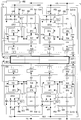
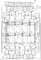
- FIG. 1 is a schematic diagram illustrating a configuration of a liquid crystal display device according to Example 1.
- FIG. It is a schematic diagram which shows the connection state of a some display control board
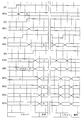
- FIG. 3 is a circuit diagram illustrating a configuration example of a part of FIG. 2. 3 is a timing chart illustrating the operation of each display control board in the first embodiment.
- 6 is a schematic diagram illustrating a configuration of a liquid crystal display device according to Embodiment 2.
- FIG. 10 is a timing chart showing the operation of each display control board in Example 2.
- 6 is a schematic diagram illustrating a configuration of a liquid crystal display device according to Example 3.
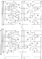
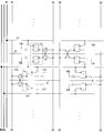
- FIG. It is a circuit diagram which shows a part of liquid crystal panel of FIG. It is a circuit diagram which shows the center part of the liquid crystal panel of FIG.
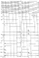
- FIG. 10 is a timing chart illustrating a method for driving the liquid crystal panel of FIGS. 8 and 9.
- FIG. 11 is a circuit diagram showing a distribution of pixel polarities (part of FIG. 8) by the driving method of FIG.
- FIG. 11 is a circuit diagram showing a distribution of pixel polarities (portion of FIG. 9) by the driving method of FIG.
- FIG. 11 is a circuit diagram showing a distribution of light and dark areas (portion of FIG. 8) by the driving method of FIG.
- FIG. 11 is a circuit diagram showing a distribution of light and dark areas (portion of FIG. 9) by the driving method of FIG.
- the liquid crystal display device LCD has a video standard (for example, horizontal 7680 pixels ⁇ vertical 4320 pixels) having a pixel number (8K4K) that is 16 times the number of full HD pixels (horizontal 1920 pixels ⁇ vertical 1080 pixels).
- a video standard for example, horizontal 7680 pixels ⁇ vertical 4320 pixels
- a pixel mapping circuit PMC for example, four display control boards (timing controller boards) DC1 to DC4, a liquid crystal panel LCP, and four gate drivers GD1 to GD4, two source drivers SD1 to SD2, four CS drivers CD1 to CD4, three power supply devices (not shown) connected to different commercial power sources, power supply controller (not shown), backlight BL, back A write driver BLD and a backlight controller BLC are provided.
- the four display control boards (so-called timing controller boards) DC1 to DC4 perform display control of one liquid crystal panel LCP (particularly, a large high-definition liquid crystal panel).
- the video signal input to the input processing circuit IPC may be a video signal (for example, Super Hi-Vision) having a block scan format of 8K4K pixels, or a video signal having a number of 8K4K pixels of a multi-display format. Also good. Of course, it may be a video signal having the number of 4K2K pixels or a video signal having the number of 2K1K pixels (the number of full HD pixels).
- the block scan format is a method in which one frame (entire image having 8K4K pixels) is divided into 16 coarse (full HD pixel) whole images (so-called thinned images) and transmitted.
- each of the 16 video signals Qa1 to Qa16 input to the input processing circuit IPC is a rough overall image (the number of full HD pixels).
- the multi-display format is a system in which one frame (entire image having the number of 8K4K pixels) is divided into 16 without changing the fineness of the frame, and divided into 16 partial images for transmission.
- each of the 16 video signals Qa1 to Qa16 input to the input processing circuit IPC is a fine partial image (the number of full HD pixels).
- the input processing circuit IPC performs video data synchronization processing, ⁇ correction processing, color temperature correction processing, color gamut conversion processing, and the like, and outputs video signals Qb1 to Qb16 to the pixel mapping circuit PMC.
- the display control board DC1 includes two video processing circuits EP1 and EP2 and two timing controllers TC1 and TC2, and the display control board DC2 includes two video processing circuits EP3 and EP4 and two timing controllers TC3 and TC4.
- the display control board DC3 includes two video processing circuits EP5 and EP6 and two timing controllers TC5 and TC6, and the display control board DC4 includes two video processing circuits EP7 and EP8 and two timing controllers TC7 and TC8. Is provided.
- the pixel mapping circuit PMC generates two video signals (2K2K pixel number) corresponding to the left half AR1 of the local area 1 (upper left region when the liquid crystal panel LCP is divided into four parts in the upper, lower, left and right directions). Divided into signals Qc1 and Qc2) and output to the video processing circuit EP1 of the display control board DC1, and two video signals (2K2K pixels) corresponding to the right half AR2 of the local area 1 (the number of full HD pixels) The video signal Qc3, Qc4) is divided and output to the video processing circuit EP2 of the display control board DC1, and the video corresponding to the left half AR3 of the local area 2 (the upper right area when the liquid crystal panel LCP is divided into four parts vertically and horizontally) The signal (number of 2K2K pixels) is divided into two (video signals Qc5 and Qc6 having the number of full HD pixels) and output to the video processing circuit EP3 of the display control board DC2.
- the video signal (2K2K pixel number) corresponding to the right half AR4 of the local area 2 is divided into two (video signals Qc7 and Qc8 having the number of full HD pixels) and supplied to the video processing circuit EP4 of the display control board DC2. And outputs two video signals (2K2K pixel number) corresponding to the left half AR5 of the local area 3 (lower left region when the liquid crystal panel LCP is divided into four parts vertically and horizontally) (the video signal Qc9 ⁇ Qc10) and output to the video processing circuit EP5 of the display control board DC3, and two video signals (2K2K pixel number) corresponding to the right half AR6 of the local area 3 (the video signal Qc11.
- the video signal (number of 2K2K pixels) corresponding to the left half AR7 is divided into two (video signals Qc13 and Qc14 having the number of full HD pixels) and output to the video processing circuit EP7 of the display control board DC4.
- the video signal corresponding to the right half AR8 (2K2K pixel count) is divided into two (video signals Qc15 and Qc16 having the full HD pixel count) and output to the video processing circuit EP8 of the display control board DC4.
- the pixel mapping circuit PMC outputs a synchronization signal SYS (vertical synchronization signal, horizontal synchronization signal, clock signal, data enable signal, polarity inversion signal, etc.) to the timing controller TC1 of the display control board DC1, and receives this timing.
- the controller TC1 transmits this synchronization signal SYS to the inter-substrate shared line SSL connected to the display control substrates DC1 to DC4.
- the timing controller TC1 receives the synchronization signal SYS received from the pixel mapping circuit PMC and cooperates with the video processing circuit EP1 to perform video processing such as gradation conversion processing and frame rate conversion (FRC) processing on the video signals Qc1 and Qc2.
- the source control signal SC1 is output to the source driver substrate (not shown) corresponding to AR1
- the gate control signal GC1 is output to the gate driver substrate (not shown) of the gate driver GD1
- the CS driver CD1 is output.
- the CS control signal CC1 is output.
- the timing controller TC2 receives the synchronization signal SYS transmitted from the timing controller TC1 via the inter-substrate shared line SSL, cooperates with the video processing circuit EP2, performs the video processing on the video signals Qc3 and Qc4, and then performs AR2
- a source control signal SC2 is output to a source driver board (not shown) corresponding to
- the timing controller TC3 receives the synchronization signal SYS transmitted from the timing controller TC1 via the inter-substrate shared line SSL, cooperates with the video processing circuit EP3, performs the video processing on the video signals Qc5 and Qc6, and then performs AR3.
- a source control signal SC3 is output to a source driver board (not shown) corresponding to
- the timing controller TC4 receives the synchronization signal SYS transmitted from the timing controller TC1 via the inter-substrate shared line SSL, cooperates with the video processing circuit EP4, performs the video processing on the video signals Qc7 and Qc8, and then performs AR4.
- the source control signal SC4 is output to the source driver board (not shown) corresponding to the above, the gate control signal GC2 is output to the gate driver board (not shown) of the gate driver GD2, and the CS control signal CC2 is sent to the CS driver CD2. Output.
- the timing controller TC5 receives the synchronization signal SYS transmitted from the timing controller TC1 via the inter-substrate shared line SSL, cooperates with the video processing circuit EP5, performs the video processing on the video signals Qc9 and Qc10, and then performs AR5.
- the source control signal SC5 is output to the source driver board (not shown) corresponding to the above, the gate control signal GC3 is output to the gate driver board (not shown) of the gate driver GD3, and the CS control signal CC3 is sent to the CS driver CD3. Output.
- the timing controller TC6 receives the synchronization signal SYS transmitted from the timing controller TC1 via the inter-substrate shared line SSL, cooperates with the video processing circuit EP6, performs the video processing on the video signals Qc11 and Qc12, and then performs AR6.
- a source control signal SC6 is output to a source driver board (not shown) corresponding to
- the timing controller TC7 receives the synchronization signal SYS transmitted from the timing controller TC1 via the inter-substrate shared line SSL, cooperates with the video processing circuit EP7, performs the video processing on the video signals Qc13 and Qc14, and then performs AR7.
- a source control signal SC7 is output to a source driver board (not shown) corresponding to
- the timing controller TC8 receives the synchronization signal SYS transmitted from the timing controller TC1 via the inter-substrate shared line SSL, cooperates with the video processing circuit EP8, performs the video processing on the video signals Qc15 and Qc16, and then performs AR8.
- the source control signal SC8 is output to the source driver board (not shown) corresponding to the above, the gate control signal GC4 is output to the gate driver board (not shown) of the gate driver GD4, and the CS control signal CC4 is sent to the CS driver CD4. Output.
- the source control signals SC1 to SC8 include a data signal, a data enable signal (DE signal), a source start pulse, and a source clock.
- the gate control signals GC1 to GC4 include an initial signal, a gate start pulse, and a gate. A clock is included.
- the gradation conversion processing corresponds to a combination of high-speed display processing (QS processing), panel vertical division driving (described in detail below), and 1 V inversion driving of data signal lines (described in detail below).
- QS processing high-speed display processing
- panel vertical division driving panel vertical division driving
- 1 V inversion driving of data signal lines described in detail below.
- the tone correction processing according to the pixel position may be included.
- each video processing circuit obtains a motion vector using any one of the 16 video signals Qa1 to Qa16 (the entire image with a rough HD, which is the number of full HD pixels), and video A partial image (the number of full HD pixels) for interpolation may be generated using a corresponding one of the signals Qc1 to Qc16 (a fine partial image having the number of full HD pixels).
- the DE signal (for 1920 lines) extends one clock (for one line) and reaches 1921 lines. Therefore, when the width of the DE signal is monitored and it becomes 1921 lines, it is possible to perform error correction processing for starting up the DE signal with a delay of one clock. That is, the above-mentioned effective signal is supplied to the display control board DC1 to which a data signal (for example, video signals Qc1 to Qc4) and a valid signal (DE) indicating a valid period of the data signal are input via an input interface (for example, HDMI).
- a data signal for example, video signals Qc1 to Qc4
- DE valid signal
- a detection unit that detects at least one of the content of the data signal obtained based on the signal and the active period of the effective signal, and a correction unit that corrects the phase shift of the effective signal according to the detection result of the detection unit. Provide. By doing this, it is possible to eliminate the problem of the data signal (particularly the problem that is likely to occur when using HDMI) due to the phase shift of the effective signal.
- the display control boards DC1 to DC4 synchronize their operations by exchanging or sharing various signals between the boards.
- the display control board DC1 which is the master, sends an RDY (ready) signal to the slave display control board DC2, and the display control board DC2 that receives the slave sends the RDY signal to the slave as soon as the preparation is completed.
- the display control board DC3 that has received and received the RDY signal is sent to the slave display control board DC4 as soon as preparation is completed, and the display control board DC4 that has received this is ready. Then, the RDY signal is returned to the display control board DC1.
- the display control board DC1 transmits an operation start (SRST) signal simultaneously to the display control boards DC2 to DC4 via the inter-substrate shared line SSL.
- the timing controller TC1 of the display control board DC1 receives the synchronization signal SYS received from the pixel mapping circuit PMC via the inter-substrate shared line SSL, and the timing controllers TC2 to TC8. Send to all. More details are as follows.
- the display control board DC1 includes a local power supply circuit PC1, a video connector CN1 to which video signals Qc1 to Qc4 are input, a synchronization connector cn1, a synchronization circuit SYC1, timing controllers TC1 and TC2, and a video processing circuit EP1. ⁇ Equipped with EP2.
- the local power supply circuit PC1 is connected to the synchronization circuit SYC1, the timing controllers TC1 and TC2, and the video processing circuits EP1 and EP2 (not shown).
- the synchronization circuit SYC1 is connected to the synchronization connector cn1 and the timing controllers TC1 and TC2.
- the timing controller TC1 is connected to the video processing circuit EP1 and the timing controller TC2, and the timing controller TC2 is connected to the video processing circuit EP2 and the timing controller TC1.
- the display control board DC2 includes a local power supply circuit PC2, a video connector CN2 to which video signals Qc5 to Qc8 are input, a synchronization connector cn2, a synchronization circuit SYC2, timing controllers TC3 and TC4, and video processing circuits EP3 and EP4.
- the local power supply circuit PC2 is connected to the synchronization circuit SYC2, the timing controllers TC3 and TC4, and the video processing circuits EP3 and EP4 (not shown).
- the synchronization circuit SYC2 is connected to the synchronization connector cn2 and the timing controllers TC3 and TC4.
- the timing controller TC3 is connected to the video processing circuit EP3 and the timing controller TC4, and the timing controller TC4 is connected to the video processing circuit EP4 and the timing controller TC3.
- the display control board DC3 includes a local power supply circuit PC3, a video connector CN3 to which video signals Qc9 to Qc12 are input, a synchronization connector cn3, a synchronization circuit SYC3, timing controllers TC5 and TC6, and video processing circuits EP5 and EP6.
- the local power supply circuit PC3 is connected to the synchronization circuit SYC3, the timing controllers TC5 and TC6, and the video processing circuits EP5 and EP6 (not shown).
- the synchronization circuit SYC3 is connected to the synchronization connector cn3 and the timing controllers TC5 and TC6.
- the timing controller TC5 is connected to the video processing circuit EP5 and the timing controller TC6, and the timing controller TC6 is connected to the video processing circuit EP6 and the timing controller TC5.
- the display control board DC4 includes a local power supply circuit PC4, a video connector CN4 to which video signals Qc13 to Qc16 are input, a synchronization connector cn4, a synchronization circuit SYC4, timing controllers TC7 and TC8, and video processing circuits EP7 and EP8.
- the local power supply circuit PC4 is connected to the synchronization circuit SYC4, the timing controllers TC7 and TC8, and the video processing circuits EP7 and EP8 (not shown).
- the synchronization circuit SYC4 is connected to the synchronization connector cn4 and the timing controllers TC7 and TC8.
- the timing controller TC7 is connected to the video processing circuit EP7 and the timing controller TC8, and the timing controller TC8 is connected to the video processing circuit EP8 and the timing controller TC7.
- the display control board DC1 operates as a master, and the display control boards DC2 to DC4 operate as slaves.
- the video connectors CN1 to CN4 are respectively connected to the synchronization shared line SSL1, and the synchronization connectors cn1 to cn4 are connected to the reset shared line SSL2.
- the preparation signal RDYa is made active (preparation completion signal) and transmitted to the synchronization circuit SYC2 via the synchronization connectors cn1 and cn2.
- the synchronization circuit SYC2 activates the preparation signal RDYb (preparation completion signal) The data is transmitted to the synchronization circuit SYC4 via cn2 and cn4.
- the synchronization circuit SYC4 When the preparation signal RDYb from the synchronization circuit SYC2 is active and the power supply voltage signal from the local power supply circuit PC4 is equal to or higher than the threshold level, the synchronization circuit SYC4 activates the preparation signal RDYc (preparation completion signal) The data is transmitted to the synchronization circuit SYC3 via cn4 and cn3.
- the preparation signal RDYc from the synchronization circuit SYC4 is active and the power supply voltage signal from the local power supply circuit PC3 is equal to or higher than the threshold level
- the synchronization circuit SYC3 sets the preparation signal RDYd to be active (preparation completion signal).
- the data is transmitted to the synchronization circuit SYC1 via cn3 and cn1.
- the synchronization circuit SYC1 deactivates the reset signal SRST (reset release signal), transmits the reset signal SRST to the reset shared line SSL2 via the synchronization connector cn1, and the timing controller TC2 Send to.
- the reset release signal is simultaneously transmitted to the synchronization circuits SYC2 to SYC4 via the reset shared line SSL2 and the synchronization connectors cn2 to cn4.
- the synchronization circuit SYC2 Upon receiving the reset release signal, the synchronization circuit SYC2 activates the reset release signal RSTb to the timing controllers TC3 and TC4, thereby completing the operation preparation of the timing controllers TC3 and TC4.
- the synchronization circuit SYC4 that has received the reset release signal activates the reset release signal RSTc to the timing controllers TC7 and TC8, thereby completing the operation preparation of the timing controllers TC7 and TC8.
- the synchronization circuit SYC3 that has received the reset release signal activates the reset release signal RSTd to the timing controllers TC5 and TC6, thereby completing the operation preparation of the timing controllers TC5 and TC6.
- the synchronization signal SYS (vertical synchronization signal, horizontal synchronization signal, clock signal, data enable signal, polarity inversion signal, etc.) input to the timing controller TC1 is sent from the timing controller TC1 to the video connector CN1, the synchronization shared line SSL1, and the like.
- the video data is transmitted to the timing controllers TC2 to TC8 via the video connectors CN2 to CN4, whereby the synchronization operation of the timing controllers TC1 to TC8 is started.
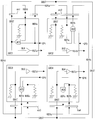
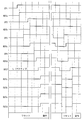
- FIG. 3 is a circuit diagram showing a specific example of FIG. 1, and FIG. 4 is a timing chart showing the operation of the configuration of FIG.
- the synchronization circuit SYC1 includes an AND circuit AC1 and a buffer circuit BU1
- the synchronization circuit SYC2 includes an AND circuit AC2 and a buffer circuit BU2
- the synchronization circuit SYC3 includes an AND circuit AC3 and a buffer circuit.
- the synchronization circuit SYC4 includes an AND circuit AC4 and a buffer circuit BU4.
- the preparation signal RDYa becomes active “H” (preparation completion signal), and the AND of the synchronization circuit SYC2 via the synchronization connectors cn1 and cn2. It is transmitted to the circuit AC2.
- the AND circuit AC2 receives the preparation signal RDYa and the power supply voltage signal CP2 from the local power supply circuit PC2, and when both become active “H”, the preparation signal RDYb becomes active “H” (preparation completion signal). Are transmitted to the AND circuit AC4 of the synchronous circuit SYC4 via the synchronous connectors cn2 and cn4.
- the AND circuit AC4 receives the preparation signal RDYb and the power supply voltage signal CP4 from the local power supply circuit PC4, and when both become active “H”, the preparation signal RDYc becomes active “H” (preparation completion signal). Are transmitted to the AND circuit AC3 of the synchronization circuit SYC3 via the synchronization connectors cn4 and cn3.
- the AND circuit AC3 is supplied with the preparation signal RDYc and the power supply voltage signal CP3 from the local power supply circuit PC3. When both become active “H”, the preparation signal RDYd becomes active “H” (preparation completion signal). Are transmitted to the AND circuit AC1 of the synchronization circuit SYC1 via the synchronization connectors cn3 and cn1.
- the AND circuit AC1 receives the preparation signal RDYd and the power supply voltage signal CP1 from the local power supply circuit PC1.
- the preparation signal RDYd becomes active “H”
- the reset signal SRST is inactive “H” (reset release) Signal).
- the reset release signal is transmitted to the buffer circuit BU1, and simultaneously transmitted to the buffer circuits BU2 to BU4 via the connector cn1, the reset shared line SSL2, and the connectors cn2 to cn4, and the reset release signal from the buffer circuits BU1 to BU4.
- RSTa to RSTd are active “H”.
- the buffer circuits BU1 to BU4 perform impedance conversion.
- the synchronous operation can be started after all the operation preparations of the display control boards DC1 to DC4 are completed, and the video failure at the time of turning on the power or returning from the fail safe can be avoided. it can.
- timing controllers are used, but four or two may be used according to the division form of the display unit. Further, various signals included in the synchronization signal SYS may be determined as necessary.
- the local power supply circuits PC1 to PC4 may be activated at the same time (turned on) or sequentially activated.
- the fail-safe signal transmitted from the display control board on which the abnormality has occurred is transmitted to all the other control boards. It is transmitted to the display control board (cyclic transmission or simultaneous transmission via a shared line), and all the control display boards are instantaneously in a self-running state (black display) mode. Thereby, the video failure is avoided.
- Each of the display control boards DC1 to DC4 individually generates various drive power supplies, and the lines to which the same kind (same potential / same phase) of drive power is supplied are connected between the display control boards via the current limiting circuit. Connected with. In this way, it is possible to prevent the overcurrent from flowing to various drivers and the display control board due to a difference in the rise timing between the boards while adjusting the same type of drive power supply.
- the liquid crystal panel LCP includes an active matrix substrate, a liquid crystal layer (not shown), and a counter substrate (not shown).
- the active matrix substrate includes a plurality of pixel electrodes (not shown) and a plurality of TFTs (thin film transistors, FIG. Scanning signal lines Ga to Gd extending in the row direction (the direction along the long side of the panel), a plurality of data signal lines Sa to Sd extending in the column direction, and a storage capacitor wiring (CS wiring extending in the row direction).
- CSa to CSd and CS trunk wires Ma to Mh extending in the column direction are provided, and a common electrode (not shown), a color filter, and a black matrix (not shown) are provided on the counter substrate. .
- the gate driver GD1 includes a plurality of gate driver chips I provided along one of the two short sides of the upper half of the liquid crystal panel LCP and arranged in the column direction.
- the vertical driver GD2 includes a plurality of gate driver chips I provided along the other of the two short sides of the upper half of the liquid crystal panel LCP and arranged in the column direction.
- the gate driver GD3 includes a plurality of gate driver chips I provided along one of the two short sides of the lower half of the liquid crystal panel LCP and arranged in the column direction.
- the vertical driver GD4 is provided along the other of the two short sides of the lower half of the liquid crystal panel LCP, and includes a plurality of gate driver chips I arranged in the column direction.
- the scanning signal lines provided in the upper half of the panel are driven by the gate drivers GD1 and GD2, and the scanning signal lines provided in the lower half of the panel are driven by the gate drivers GD3 and GD4. That is, one scanning signal line is connected to two gate drivers arranged on both sides thereof, and a scanning (pulse) signal having the same phase is supplied from the two gate drivers to the one scanning signal line. By so doing, it is possible to suppress variations in signal dullness (the degree of signal dullness varies depending on the position in the row direction) caused by CR (time constant) of the scanning signal line.
- the source driver SD1 is provided along one long side of the upper half of the liquid crystal panel LCP, and 48 source driver chips J arranged in the row direction (the number of output terminals of one source driver chip is 960), 4 source driver boards (not shown) are included (12 source driver chips J are mounted on one source driver board).
- the source driver SD2 is provided along one long side of the lower half of the liquid crystal panel LCP, and 48 source driver chips J arranged in the row direction (the number of output terminals of one source driver chip is 960). And four source driver boards (not shown) (12 source driver chips J are mounted on one source driver board).
- Each data signal line provided in the upper half of the panel is driven by the source driver SD1, and each data signal line provided in the lower half of the panel is driven by the source driver SD2.
- the data signal line Sa is driven by the source driver SD1
- the data signal line Sc is driven by the source driver SD2.
- the source driver chip J cannot be arranged along the long side of the panel due to the space, it is arranged on the short side of the panel with sufficient space (the source driver chip J and the gate driver chip I are arranged side by side). Can be arranged).
- a relay line that connects the data signal line and the source terminal on the short side of the panel is provided on the counter substrate side, or other than the source layer of the active matrix substrate (the source / drain electrode formation layer of the TFT) It can also be provided in a lower layer (gate layer) of the gate insulating film or a layer between the source layer and the ITO layer (pixel electrode formation layer).
- the liquid crystal panel LCP is provided with two data signal lines corresponding to the upper half (first area, upstream side of the panel) of one pixel column, and the lower half (second area, panel of the panel).
- a so-called upper and lower divided double source structure four data signal lines are provided per pixel column, and four scanning signal lines are selected simultaneously, provided with two data signal lines corresponding to the downstream side) 4x speed drive is possible.
- the liquid crystal panel LCP is a so-called multi-pixel method in which at least two pixel electrodes are provided in one pixel, and the viewing angle characteristics can be enhanced by a bright region and a dark region formed in one pixel. ing.
- the scanning signal lines Ga and Gb and the storage capacitor lines CSa and CSb are provided in the upper half (upstream side) of the panel, and the lower half (downstream side) of the panel.
- the upper half (upstream side) of one pixel column PL1 includes two pixels Pa and Pb adjacent in the column direction.
- the lower half (downstream side) includes two pixels Pc and Pd adjacent in the column direction, and data signal lines Sa and Sb are provided corresponding to the upper half (upstream side) of the pixel column PL1, and the pixel column Data signal lines Sc and Sd are provided corresponding to the lower half (downstream side) of PL1.
- the TFT 12A connected to the pixel electrode 17A and the TFT 12a connected to the pixel electrode 17a are connected to the data signal line Sa and the scanning signal line Ga, respectively.
- 17A forms the storage capacitor line CSn and the storage capacitor CA
- the pixel electrode 17a forms the storage capacitor line CSa and the storage capacitor Ca
- the pixel electrode 17B out of the two pixel electrodes 17B and 17b included in the pixel Pb.
- the TFT 12B to be connected and the TFT 12b to be connected to the pixel electrode 17b are connected to the data signal line Sb and the scanning signal line Gb, the pixel electrode 17B forms the storage capacitor line CSa and the storage capacitor CB, and the pixel electrode 17b has the storage capacitor.
- a wiring CSb and a storage capacitor Cb are formed, and two pixel electrodes included in the pixel Pc are further formed.
- 7C and 17c, the TFT 12C connected to the pixel electrode 17C and the TFT 12c connected to the pixel electrode 17c are respectively connected to the data signal line Sc and the scanning signal line Gc, and the pixel electrode 17C includes the storage capacitor line CSm and the storage capacitor CC.
- the pixel electrode 17c forms the storage capacitor line CSc and the storage capacitor Cc, and the TFT 12D connected to the pixel electrode 17D and the TFT 12d connected to the pixel electrode 17d out of the two pixel electrodes 17D and 17d included in the pixel Pd.
- Each is connected to the data signal line Sd and the scanning signal line Gd, the pixel electrode 17D forms a storage capacitor line CSc and a storage capacitor CD, and the pixel electrode 17d forms a storage capacitor line CSd and a storage capacitor Cd.
- Four scanning signal lines Ga to Gd are simultaneously selected.
- the data signal lines Sa and Sc are arranged in the column direction at the left end, and the data signal lines Sb and Sd are arranged in the column direction at the right end, and the pixel column PL2 adjacent to the pixel column PL1.
- the data signal lines SA and SC are arranged at the left end in the column direction, and the data signal lines SB and SD are arranged at the right end in the column direction.
- the two pixel electrodes included in the pixel adjacent to the pixel electrode Pa are connected to the data signal line SB via separate TFTs, and the two pixels included in the pixel adjacent to the pixel electrode Pb.
- the electrodes are connected to the data signal line SA via separate TFTs, and the two pixel electrodes included in the pixel adjacent to the pixel electrode Pc are connected to the data signal line SD via separate TFTs, and the pixel electrode Pd And two pixel electrodes included in adjacent pixels are connected to the data signal line SC via separate TFTs.
- the configuration near the boundary between the upper half (first region) and the lower half (second region) is as shown in FIG. That is, of the two pixel electrodes 17X and 17x included in the pixel Px located at the bottom of the first region, the TFT 12X connected to the pixel electrode 17X and the TFT 12x connected to the pixel electrode 17x are respectively connected to the data signal line Sb and the scanning signal line.
- the pixel electrode 17X forms a storage capacitor with a storage capacitor line CSi
- the pixel electrode 17x forms a storage capacitor line with a storage capacitor line CSm
- the pixel Pc is located at the top of the second region. Yes.
- the CS trunk line Ma (first trunk line) and the CS trunk line Mb are provided close to one of the two short sides of the upper half of the active matrix substrate, and are in different phases by the CS driver CD1. Driven.
- the CS trunk wiring Mc (third trunk wiring) and the CS trunk wiring Md are provided close to the other of the two short sides of the upper half of the active matrix substrate so that the CS driver CD2 has different phases. Driven by.
- the CS trunk wiring Me / CS trunk wiring Mf (second trunk wiring) is provided in proximity to one of the two short sides of the lower half of the active matrix substrate, and each has a different phase by the CS driver CD3. Driven.
- the CS trunk wiring Mg / CS trunk wiring Mh (fourth trunk wiring) is provided close to the other of the two short sides of the lower half of the active matrix substrate, and the CS driver CD4 is in a different phase. Driven by.
- One storage capacitor line is connected to two CS trunk lines arranged on both sides thereof, and a modulation (pulse) signal having the same phase is transmitted from the two CS trunk lines to the one storage capacitor line. Is supplied.
- the storage capacitor line CSa is connected to the CS trunk lines Ma and Mc
- the storage capacitor line CSb is connected to the CS trunk lines Mb and Md
- the storage capacitor line CSc is connected to the CS trunk lines Me and Mg
- the storage capacitor line CSd is connected to CS trunk lines Mf and Mh. Therefore, for example, when the potentials of the CS trunk lines Ma and Mb are controlled to be in opposite phases, the potentials of the storage capacitor lines CSa and CSb are also reversed in phase, and in the pixel Pb, the pixel electrode of the two pixel electrodes 17B and 17b.
- the polarity of the data signal supplied to one data signal line is inverted every one vertical scanning period (1V), and two data signal lines provided corresponding to one pixel column in the same vertical scanning period.
- the polarity of the data signal supplied to one and the other is opposite.
- each data signal line is inverted by 1V (that is, the polarity inversion period is lengthened and power consumption is reduced), and the polarity distribution of the pixels in the screen is inverted by dots (thus turning off the TFT). Flicker caused by the pull-in voltage generated at the same time can be suppressed).
- the driving method of the part shown in FIGS. 8 and 9 of the liquid crystal panel is shown in the timing chart of FIG. 10 and the schematic diagrams of FIGS.
- a positive data signal potential is supplied to the data signal lines Sa, SA, Sc, and SC during one vertical scanning period, and the data signal lines Sb, SB, Sd, and SD are During one vertical scanning period, a negative data signal potential is supplied.
- Simultaneous scanning of the scanning signal lines Ga to Gd starts at time t0, and simultaneous scanning of the scanning signal lines Ga to Gd ends at time t1 1H (vertical scanning period) after t0.
- a positive data signal potential is written to the pixel electrodes 17A and 17a
- a negative data signal potential is written to the pixel electrodes 17B and 17b
- a positive data signal potential is written to the pixel electrodes 17C and 17c.
- a negative data signal potential is written to the pixel electrodes 17D and 17d.
- the potential of the storage capacitor line CSn is shifted to the L (Low) side by the modulation signal sent from the CS trunk line Mb.
- the effective potential until the scan is lower than the written data signal potential (+) (becomes a dark region).
- the potential of the storage capacitor line CSa is shifted to the H (High) side by the modulation signal sent from the CS drivers CD1 and CD2 via the CS trunk lines Ma and Mc, and accordingly, the pixel electrode 17a And the effective potential until the next scanning rises higher than the written data signal potential (+) (becomes a bright region).
- the potential of the pixel electrode 17B rises (because the potential of the storage capacitor line CSa shifts to the H side), and the effective potential until the next scan is higher than the written data signal potential ( ⁇ ). It rises (becomes a dark area).
- the potential of the storage capacitor line CSm is shifted to the L (Low) side by the modulation signal sent from the CS trunk line Mm, and accordingly, the potential of the pixel electrode 17C drops down to the next scan. Is lower than the written data signal potential (+) (becomes a dark region).
- the potential of the storage capacitor line CSc is shifted to the H (High) side by a modulation signal sent from the CS drivers CD3 and CD4 via the CS trunk lines Me and Mg, and accordingly, the pixel electrode 17c And the effective potential until the next scanning rises higher than the written data signal potential (+) (becomes a bright region).
- the potential of the storage capacitor line CSb is shifted to the L side by the modulation signal sent from the CS drivers CD1 and CD2 via the CS trunk lines Mb and Md, and accordingly, the potential of the pixel electrode 17b is The effective potential until the next scan is lowered (becomes a bright region) than the written data signal potential ( ⁇ ).
- the scanning signal line Ga is the nth line counting from the upper long side of the panel and the scanning signal line Gb is the n + 1th line (FIGS. 8 to 14).
- the scanning signal line Gc is the n + 2160th line from the upper long side and the scanning signal line Gb is the (n + 2161) th line from the upper long side, and the scanning signal provided in the upper half of the panel. If the data signal of the nth frame of the Nth frame is written to the line Ga, the scanning signal line Gc provided in the lower half of the panel has the (n + 2160) th line of the (N ⁇ 1) th frame as the previous frame. Data signal is written. By doing so, the feeling of display deviation at the top and bottom of the panel is suppressed.
- the backlight controller BLC receives the video signal QBL output from the pixel mapping circuit PMC, outputs a backlight control signal to the backlight driver BD, and the backlight BL is driven by the backlight driver BD.
- the backlight BL is divided into a plurality of parts, and the brightness is individually adjusted according to the video signal QBL (active backlight).
- the power supply controller monitors the supply power level of the commercial power supply connected to each of the three power supply circuits, and if for some reason one or more commercial power supplies have an abnormality (decreased supply power level) ,
- One or a plurality of normal commercial power sources for power lines to the backlight BL for example, three systems for R, B, and G
- power lines to the display control boards DC1 to DC4 for example, one system
- the abnormality occurrence signal is output to the backlight controller BLC.
- the backlight controller BLC receives this abnormality occurrence signal, the backlight controller BLC outputs a control signal that lowers the upper limit of the brightness of the backlight BL to the backlight driver BD.
- the power supply controller When the power supply controller eliminates the need for three power supply circuits and a configuration in which only one power supply circuit connected to a commercial power supply is provided is possible, the power supply controller 1
- the supply power level of one commercial power supply is monitored, and if an abnormality occurs in this commercial power supply (decrease in the supply power level) for some reason, an abnormality occurrence signal is output to the backlight controller BLC (this abnormality occurrence signal is
- the received backlight controller BLC can output a control signal that lowers the upper limit of the luminance of the backlight BL to the backlight driver BD).
- TTL level signals and CMOS level signals are used as the preparation signals RDYa to RDYd, the reset signal SRST, and the synchronization signal SYS, but the present invention is not limited to this.
- a differential (system) signal such as LVDS can be used as at least one of the preparation signals RDYa to RDYd, the reset signal SRST, and the synchronization signal SYS.
- differential signals in FIG. 5, the differential signal path is indicated by a thick line
- the display control boards DC1 to DC4 are provided with conversion circuits LCC that convert the differential signals into single-end signals.
- Example 3 When it is necessary to synchronize the backlight of the liquid crystal display device with the driving of the liquid crystal panel (for example, in the case of 3D support or active backlight), the backlight control substrates BCS1 and BCS2 are added to the liquid crystal display device of FIG. Can be provided as shown in FIG.
- the backlight control board BCS1 is provided with the synchronization circuit SYC5, the power supply circuit PC5, the backlight control circuit BC1 to which the video signals Qc1 to Qc8 are input, the backlight driver BD1, and the backlight B1, and the backlight control board BCS2 ,
- the preparation signal RDYa is made active (preparation completion signal) and transmitted to the synchronization circuit SYC2 via the synchronization connectors cn1 and cn2.
- the synchronization circuit SYC2 activates the preparation signal RDYb (preparation completion signal) The data is transmitted to the synchronization circuit SYC4 via cn2 and cn4.
- the synchronization circuit SYC4 When the preparation signal RDYb from the synchronization circuit SYC2 is active and the power supply voltage signal from the local power supply circuit PC4 is equal to or higher than the threshold level, the synchronization circuit SYC4 activates the preparation signal RDYc (preparation completion signal) The data is transmitted to the synchronization circuit SYC3 via cn4 and cn3.
- the synchronization circuit SYC3 sets the preparation signal RDYd to be active (preparation completion signal). The data is transmitted to the synchronization circuit SYC6 via cn3.
- the synchronization circuit SYC6 sets the preparation signal RDYe active (preparation completion signal). Send to SYC5. If the preparation signal RDYe from the synchronization circuit SYC6 is active and the power supply voltage signal from the local power supply circuit PC5 is equal to or higher than the threshold level, the synchronization circuit SYC5 activates the preparation signal RDYf (preparation completion signal), and the synchronization connector To the synchronization circuit SYC1.
- the synchronization circuit SYC1 deactivates the reset signal SRST (reset release signal), transmits the reset signal SRST to the reset shared line SSL2 via the synchronization connector cn1, and the timing controller TC2 Send to.
- the reset release signal is simultaneously transmitted to the synchronization circuits SYC2 to SYC6 via the reset common line SSL2 and the synchronization connectors cn2 to cn4.
- the synchronization circuit SYC2 Upon receiving the reset release signal, the synchronization circuit SYC2 activates the reset release signal RSTb to the timing controllers TC3 and TC4, thereby completing the operation preparation of the timing controllers TC3 and TC4.
- the synchronization circuit SYC4 that has received the reset release signal activates the reset release signal RSTc to the timing controllers TC7 and TC8, thereby completing the operation preparation of the timing controllers TC7 and TC8.
- the synchronization circuit SYC3 that has received the reset release signal activates the reset release signal RSTd to the timing controllers TC5 and TC6, thereby completing the operation preparation of the timing controllers TC5 and TC6.
- the synchronization circuit SYC6 that has received the reset release signal activates the reset release signal RSTe to the backlight control circuit BC2, thereby completing the operation preparation of the backlight control circuit BC2. Also, the synchronization circuit SYC5 that has received the reset release signal activates the reset release signal RSTf to the backlight control circuit BC1, thereby completing the preparation for operation of the backlight control circuit BC1.
- the present invention uses four display control boards, but five or more display control boards can be applied.
- the present liquid crystal display device includes one liquid crystal panel and the first to nth control boards (n is an integer of 2 or more) for controlling the liquid crystal panel, and the first control board is operable.
- n is an integer of 2 or more
- the first control board is operable.
- a preparation completion signal is transmitted to the second control board which is the next stage, and the nth control board receives the preparation completion signal from the previous stage control board and determines that it is in an operable state. Send a ready signal to the control board.
- the first control board (master) can recognize that the other control board (slave) is ready, and a plurality of units provided in one liquid crystal display device. Of synchronization between the control boards can be suppressed.
- the present liquid crystal display device may be configured such that the liquid crystal panel includes first to nth regions that are controlled by the first to nth control substrates.
- a timing controller may be provided on each of the first to nth control boards, and each timing controller may be operated in synchronization based on a synchronization signal.
- the first control board may be configured to receive a preparation completion signal from the nth control board and transmit a reset release signal to all other control boards.
- the first control board may be configured to transmit the synchronization signal to all other control boards after transmitting the reset release signal.
- a power supply circuit may be provided on each of the first to nth control boards.
- the preparation completion signal may be a differential signal.
- the synchronization signal may be a differential signal.
- the reset release signal may be a differential signal.
- a control circuit other than the first control board is provided with a synchronization circuit that generates a preparation completion signal of its own stage based on the preparation completion signal from the previous control board and the supply voltage of the power supply circuit. It can also be set as the structure which is.
- the present invention is not limited to the above-described embodiments, and those obtained by appropriately modifying the above-described embodiments based on common general technical knowledge and those obtained by combining them are also included in the embodiments of the present invention.
- the present invention can be applied to a liquid crystal television and a liquid crystal display.
- LCD Liquid crystal display device LCP Liquid crystal panel TC1 to TC8 Timing controller DC1 to DC4 Display control board SYC1 to SYC4 Synchronization circuit PC1 to PC4 Local power supply circuit CN1 to CN4 Video connector cn1 to cn4 Synchronization connector RDYa to RDYf Preparation signal SRST Reset signal SYS RSTa to RSTf Reset release signal SSL Inter-substrate shared line SSL1 Synchronization shared line SSL2 Reset shared line Pa to Pd Pixel Ga to Gd Scanning signal line 17a / 17A Pixel electrode 17b / 17B Pixel electrode 12a / 12A transistor 12b / 12B transistor Sa To Sd data signal line SA to SD data signal line AR1 to AR4 (local areas 1 and 2) first area AR5 to AR8 (local areas 3 and 4) second area
Landscapes
- Engineering & Computer Science (AREA)
- Physics & Mathematics (AREA)
- Computer Hardware Design (AREA)
- General Physics & Mathematics (AREA)
- Theoretical Computer Science (AREA)
- Chemical & Material Sciences (AREA)
- Crystallography & Structural Chemistry (AREA)
- Power Engineering (AREA)
- Control Of Indicators Other Than Cathode Ray Tubes (AREA)
Abstract
本液晶表示装置は、1つの液晶パネルと、上記液晶パネルの制御を行う第1~第n制御基板(nは2以上の整数)とを備え、第1制御基板は、動作可能状態になると次段である第2制御基板に準備完了信号を送信し、第n制御基板は、前段の制御基板からの準備完了信号を受けて自身が動作可能状態にあると判断すると、上記第1制御基板に準備完了信号を送信する。これにより、1つの液晶表示装置内に設けられた複数の制御基板間の同期不良を抑制することができる。
Description
本発明は、1つの表示装置内に複数のコントローラを設ける技術に関する。
特許文献1には、1つの表示装置内に複数のコントローラを設け、それぞれを互いに同期して(並列して)動作させる技術が開示されている。
液晶表示装置の高精細化および高速駆動化によって各コントローラで要求される電力も増大しており、例えば、電源投入後の立ち上がり時に、各コントローラの電源状態のばらつきによってコントローラ間の同期が乱れ、表示に不具合が生じるという問題があった。
本発明の目的の1つは、1つの表示装置内に設けられた複数のコントローラの同期不良を抑制することにある。
本液晶表示装置は、1つの液晶パネルと、上記液晶パネルの制御を行う第1~第n制御基板(nは2以上の整数)を備え、第1制御基板は、動作可能状態になると次段である第2制御基板に準備完了信号を送信し、第n制御基板は、前段の制御基板からの準備完了信号を受けて自身が動作可能状態にあると判断すると上記第1制御基板に準備完了信号を送信する。
上記液晶表示装置によれば、第1制御基板(マスター)は、他の制御基板(スレーブ)が準備完了になっていることを認識することができ、1つの液晶表示装置内に設けられた複数の制御基板間の同期不良を抑制することができる。
上記構成によれば、1つの液晶表示装置内に設けられた複数の制御基板間の同期不良を抑制することができる。
〔実施例1〕
本実施の形態にかかる液晶表示装置LCDは、フルHD画素数(横1920画素×縦1080画素)の16倍の画素数(8K4K)を有する映像規格(例えば、横7680画素×縦4320画素のスーパーハイビジョン)に対応するものであり、図2に示すように、入力処理回路IPC、ピクセルマッピング回路PMC、4つの表示制御基板(タイミングコントローラ基板)DC1~DC4、液晶パネルLCP、4つのゲートドライバGD1~GD4、2つのソースドライバSD1~SD2、4つのCSドライバCD1~CD4、それぞれが異なる商用電源に接続される3つの電源装置(図示せず)、電源コントローラ(図示せず)、バックライトBL、バックライトドライバBLD、およびバックライトコントローラBLCを備える。ここで、4つの表示制御基板(いわゆるタイミングコントローラ基板)DC1~DC4は、1枚の液晶パネルLCP(特に、大型高精細の液晶パネル)の表示制御を行うものである。
本実施の形態にかかる液晶表示装置LCDは、フルHD画素数(横1920画素×縦1080画素)の16倍の画素数(8K4K)を有する映像規格(例えば、横7680画素×縦4320画素のスーパーハイビジョン)に対応するものであり、図2に示すように、入力処理回路IPC、ピクセルマッピング回路PMC、4つの表示制御基板(タイミングコントローラ基板)DC1~DC4、液晶パネルLCP、4つのゲートドライバGD1~GD4、2つのソースドライバSD1~SD2、4つのCSドライバCD1~CD4、それぞれが異なる商用電源に接続される3つの電源装置(図示せず)、電源コントローラ(図示せず)、バックライトBL、バックライトドライバBLD、およびバックライトコントローラBLCを備える。ここで、4つの表示制御基板(いわゆるタイミングコントローラ基板)DC1~DC4は、1枚の液晶パネルLCP(特に、大型高精細の液晶パネル)の表示制御を行うものである。
入力処理回路IPCに入力される映像信号は、ブロックスキャンフォーマットの8K4K画素数を有する映像信号(例えば、スーパーハイビジョン)であってもよいし、マルチディスプレイフォーマットの8K4K画素数を有する映像信号であってもよい。もちろん、4K2K画素数を有する映像信号であってもよいし、2K1K画素数(フルHD画素数)を有する映像信号であってもよい。
ブロックスキャンフォーマットは、1フレーム(8K4K画素数を有する全体画像)をキメの粗い(フルHD画素数の)16枚の全体画像(いわゆる間引き画像)に分割して送信する方式である。この場合、入力処理回路IPCに入力される16本の映像信号Qa1~Qa16それぞれが、キメの粗い全体画像(フルHD画素数)となっている。
マルチディスプレイフォーマットは、1フレーム(8K4K画素数を有する全体画像)をキメの細かさを変えることなく16分割し、16枚の部分画像に分割して送信する方式である。この場合、入力処理回路IPCに入力される16本の映像信号Qa1~Qa16それぞれが、キメの細かい部分画像(フルHD画素数)となっている。
入力処理回路IPCでは、映像データの同期処理、γ補正処理、色温度補正処理、および色域変換処理等を行い、映像信号Qb1~Qb16をピクセルマッピング回路PMCに出力する。
ここで、表示制御基板DC1は、2つの映像処理回路EP1・EP2および2つのタイミングコントローラTC1・TC2を備え、表示制御基板DC2は、2つの映像処理回路EP3・EP4および2つのタイミングコントローラTC3・TC4を備え、表示制御基板DC3は、2つの映像処理回路EP5・EP6および2つのタイミングコントローラTC5・TC6を備え、表示制御基板DC4は、2つの映像処理回路EP7・EP8および2つのタイミングコントローラTC7・TC8を備える。
ピクセルマッピング回路PMCは、ローカルエリア1(液晶パネルLCPを上下左右に4分割したときの左上領域)の左半分AR1に対応する映像信号(2K2K画素数)を、2本(フルHD画素数の映像信号Qc1・Qc2)に分割して表示制御基板DC1の映像処理回路EP1に出力し、上記ローカルエリア1の右半分AR2に対応する映像信号(2K2K画素数)を、2本(フルHD画素数の映像信号Qc3・Qc4)に分割して表示制御基板DC1の映像処理回路EP2に出力し、ローカルエリア2(液晶パネルLCPを上下左右に4分割したときの右上領域)の左半分AR3に対応する映像信号(2K2K画素数)を、2本(フルHD画素数の映像信号Qc5・Qc6)に分割して表示制御基板DC2の映像処理回路EP3に出力し、上記ローカルエリア2の右半分AR4に対応する映像信号(2K2K画素数)を、2本(フルHD画素数の映像信号Qc7・Qc8)に分割して表示制御基板DC2の映像処理回路EP4に出力し、ローカルエリア3(液晶パネルLCPを上下左右に4分割したときの左下領域)の左半分AR5に対応する映像信号(2K2K画素数)を、2本(フルHD画素数の映像信号Qc9・Qc10)に分割して表示制御基板DC3の映像処理回路EP5に出力し、ローカルエリア3の右半分AR6に対応する映像信号(2K2K画素数)を、2本(フルHD画素数の映像信号Qc11・Qc12)に分割して表示制御基板DC3の映像処理回路EP6に出力し、ローカルエリア4(液晶パネルLCPを上下左右に4分割したときの右下領域)の左半分AR7に対応する映像信号(2K2K画素数)を、2本(フルHD画素数の映像信号Qc13・Qc14)に分割して表示制御基板DC4の映像処理回路EP7に出力し、上記ローカルエリア4の右半分AR8に対応する映像信号(2K2K画素数)を、2本(フルHD画素数の映像信号Qc15・Qc16)に分割して表示制御基板DC4の映像処理回路EP8に出力する。
さらに、ピクセルマッピング回路PMCは、表示制御基板DC1のタイミングコントローラTC1に同期信号SYS(垂直同期信号、水平同期信号、クロック信号、データイネーブル信号、極性反転信号等)を出力し、これを受けたタイミングコントローラTC1は、この同期信号SYSを、表示制御基板DC1~DC4に接続された基板間共有線SSLに送信する。
タイミングコントローラTC1は、ピクセルマッピング回路PMCから受けた同期信号SYSを受けて映像処理回路EP1と協働し、映像信号Qc1・Qc2に階調変換処理およびフレームレート変換(FRC)処理等の映像処理を行った後に、AR1に対応するソースドライバ基板(図示せず)にソース制御信号SC1を出力し、ゲートドライバGD1のゲートドライバ基板(図示せず)にゲート制御信号GC1を出力し、CSドライバCD1にCS制御信号CC1を出力する。
タイミングコントローラTC2は、タイミングコントローラTC1から基板間共有線SSLを介して送信された同期信号SYSを受けて映像処理回路EP2と協働し、映像信号Qc3・Qc4に上記映像処理を行った後に、AR2に対応するソースドライバ基板(図示せず)にソース制御信号SC2を出力する。
タイミングコントローラTC3は、タイミングコントローラTC1から基板間共有線SSLを介して送信された同期信号SYSを受けて映像処理回路EP3と協働し、映像信号Qc5・Qc6に上記映像処理を行った後に、AR3に対応するソースドライバ基板(図示せず)にソース制御信号SC3を出力する。
タイミングコントローラTC4は、タイミングコントローラTC1から基板間共有線SSLを介して送信された同期信号SYSを受けて映像処理回路EP4と協働し、映像信号Qc7・Qc8に上記映像処理を行った後に、AR4に対応するソースドライバ基板(図示せず)にソース制御信号SC4を出力し、ゲートドライバGD2のゲートドライバ基板(図示せず)にゲート制御信号GC2を出力し、CSドライバCD2にCS制御信号CC2を出力する。
タイミングコントローラTC5は、タイミングコントローラTC1から基板間共有線SSLを介して送信された同期信号SYSを受けて映像処理回路EP5と協働し、映像信号Qc9・Qc10に上記映像処理を行った後に、AR5に対応するソースドライバ基板(図示せず)にソース制御信号SC5を出力し、ゲートドライバGD3のゲートドライバ基板(図示せず)にゲート制御信号GC3を出力し、CSドライバCD3にCS制御信号CC3を出力する。
タイミングコントローラTC6は、タイミングコントローラTC1から基板間共有線SSLを介して送信された同期信号SYSを受けて映像処理回路EP6と協働し、映像信号Qc11・Qc12に上記映像処理を行った後に、AR6に対応するソースドライバ基板(図示せず)にソース制御信号SC6を出力する。
タイミングコントローラTC7は、タイミングコントローラTC1から基板間共有線SSLを介して送信された同期信号SYSを受けて映像処理回路EP7と協働し、映像信号Qc13・Qc14に上記映像処理を行った後に、AR7に対応するソースドライバ基板(図示せず)にソース制御信号SC7を出力する。
タイミングコントローラTC8は、タイミングコントローラTC1から基板間共有線SSLを介して送信された同期信号SYSを受けて映像処理回路EP8と協働し、映像信号Qc15・Qc16に上記映像処理を行った後に、AR8に対応するソースドライバ基板(図示せず)にソース制御信号SC8を出力し、ゲートドライバGD4のゲートドライバ基板(図示せず)にゲート制御信号GC4を出力し、CSドライバCD4にCS制御信号CC4を出力する。
なお、ソース制御信号SC1~SC8には、データ信号、データイネーブル信号(DE信号)、ソーススタートパルス、およびソースクロックが含まれ、ゲート制御信号GC1~GC4には、イニシャル信号、ゲートスタートパルスおよびゲートクロックが含まれる。
ここで、上記階調変換処理には、高速表示処理(QS処理)やパネル上下分割駆動(以下に詳述)とデータ信号線の1V反転駆動(以下に詳述)との組み合わせに対応するための、画素位置(列方向の位置)に応じた階調補正処理が含まれていてもよい。
また、上記FRC処理では、各映像処理回路で、16本の映像信号Qa1~Qa16のいずれか1つ(フルHD画素数である、キメの粗い全体画像)を用いて動きベクトルを求めるとともに、映像信号Qc1~Qc16のうち対応する1つ(フルHD画素数である、キメの細かい部分画像)を用いて内挿用の部分画像(フルHD画素数)を生成してもよい。
また、映像信号Qc1~Qc16の入力に、12ビット転送のHDMI(高精細マルチメディアインターフェース)を用いると、DE信号(1920ライン分)が1クロック(1ライン分)前に伸びて1921ライン分となるエラーが生じうるため、DE信号の幅を監視して、1921ライン分となった場合には、1クロック遅らせてDE信号を立ち上げるエラー補正処理を行うことも可能である。すなわち、入力インターフェース(例えば、HDMI)を介してデータ信号(例えば、映像信号Qc1~Qc4)と該データ信号の有効期間を示す有効信号(DE)とが入力される表示制御基板DC1に、上記有効信号に基づいて得られるデータ信号の内容および上記有効信号のアクティブ期間の少なくとも1つを検出する検出部と、該検出部の検出結果に応じて上記有効信号の位相ずれを補正する補正部とを設ける。こうすれば、有効信号の位相ずれに起因するデータ信号の不具合(特にHDMIを用いたときに生じ易い不具合)を解消することができる。
表示制御基板DC1~DC4は、基板間で各種信号をやり取りあるいは共有することで、互いの動作を同期させている。具体的には、マスターである表示制御基板DC1が、RDY(準備完了)信号をスレーブの表示制御基板DC2に送り、これを受けた表示制御基板DC2は、準備が完了し次第、RDY信号をスレーブの表示制御基板DC3に送り、これを受けた表示制御基板DC3は、準備が完了し次第、RDY信号をスレーブの表示制御基板DC4に送り、これを受けた表示制御基板DC4は、準備が完了し次第、RDY信号を表示制御基板DC1に返送する。表示制御基板DC1は、RDY信号が返送されたのを受けて、動作開始(SRST)信号を、基板間共有線SSLを介して表示制御基板DC2~DC4に一斉送信する。動作開始(SRST)信号が送信された後には、表示制御基板DC1のタイミングコントローラTC1が、ピクセルマッピング回路PMCから受けた上記同期信号SYSを、基板間共有線SSLを介して、タイミングコントローラTC2~TC8に一斉送信する。より詳細には以下のとおりである。
図1に示すように、表示制御基板DC1は、ローカル電源回路PC1、映像信号Qc1~Qc4が入力される映像コネクタCN1、同期コネクタcn1、同期回路SYC1、タイミングコントローラTC1・TC2、および映像処理回路EP1・EP2を備える。ローカル電源回路PC1は、同期回路SYC1、タイミングコントローラTC1・TC2、および映像処理回路EP1・EP2に接続され(図示せず)、同期回路SYC1は、同期コネクタcn1およびタイミングコントローラTC1・TC2に接続され、タイミングコントローラTC1は、映像処理回路EP1およびタイミングコントローラTC2に接続され、タイミングコントローラTC2は、映像処理回路EP2およびタイミングコントローラTC1に接続されている。
また、表示制御基板DC2は、ローカル電源回路PC2、映像信号Qc5~Qc8が入力される映像コネクタCN2、同期コネクタcn2、同期回路SYC2、タイミングコントローラTC3・TC4、および映像処理回路EP3・EP4を備える。ローカル電源回路PC2は、同期回路SYC2、タイミングコントローラTC3・TC4、および映像処理回路EP3・EP4に接続され(図示せず)、同期回路SYC2は、同期コネクタcn2およびタイミングコントローラTC3・TC4に接続され、タイミングコントローラTC3は、映像処理回路EP3およびタイミングコントローラTC4に接続され、タイミングコントローラTC4は、映像処理回路EP4およびタイミングコントローラTC3に接続されている。
また、表示制御基板DC3は、ローカル電源回路PC3、映像信号Qc9~Qc12が入力される映像コネクタCN3、同期コネクタcn3、同期回路SYC3、タイミングコントローラTC5・TC6、および映像処理回路EP5・EP6を備える。ローカル電源回路PC3は、同期回路SYC3、タイミングコントローラTC5・TC6、および映像処理回路EP5・EP6に接続され(図示せず)、同期回路SYC3は、同期コネクタcn3およびタイミングコントローラTC5・TC6に接続され、タイミングコントローラTC5は、映像処理回路EP5およびタイミングコントローラTC6に接続され、タイミングコントローラTC6は、映像処理回路EP6およびタイミングコントローラTC5に接続されている。
また、表示制御基板DC4は、ローカル電源回路PC4、映像信号Qc13~Qc16が入力される映像コネクタCN4、同期コネクタcn4、同期回路SYC4、タイミングコントローラTC7・TC8、および映像処理回路EP7・EP8を備える。ローカル電源回路PC4は、同期回路SYC4、タイミングコントローラTC7・TC8、および映像処理回路EP7・EP8(図示せず)に接続され、同期回路SYC4は、同期コネクタcn4およびタイミングコントローラTC7・TC8に接続され、タイミングコントローラTC7は、映像処理回路EP7およびタイミングコントローラTC8に接続され、タイミングコントローラTC8は、映像処理回路EP8およびタイミングコントローラTC7に接続されている。
なお、表示制御基板DC1はマスターとして動作し、表示制御基板DC2~DC4はスレーブとして動作する。
映像コネクタCN1~CN4はそれぞれ同期用共有線SSL1に接続され、同期コネクタcn1~cn4はリセット用共有線SSL2に接続されている。
同期回路SYC1では、ローカル電源回路PC1からの電源電圧信号が閾値レベル以上になると、準備信号RDYaをアクティブ(準備完了信号)とし、同期コネクタcn1・cn2を介して同期回路SYC2に送信する。同期回路SYC2は、同期回路SYC1からの準備信号RDYaがアクティブであり、かつローカル電源回路PC2からの電源電圧信号が閾値レベル以上であれば、準備信号RDYbをアクティブ(準備完了信号)とし、同期コネクタcn2・cn4を介して同期回路SYC4に送信する。同期回路SYC4は、同期回路SYC2からの準備信号RDYbがアクティブであり、かつローカル電源回路PC4からの電源電圧信号が閾値レベル以上であれば、準備信号RDYcをアクティブ(準備完了信号)とし、同期コネクタcn4・cn3を介して同期回路SYC3に送信する。同期回路SYC3は、同期回路SYC4からの準備信号RDYcがアクティブであり、かつローカル電源回路PC3からの電源電圧信号が閾値レベル以上であれば、準備信号RDYdをアクティブ(準備完了信号)とし、同期コネクタcn3・cn1を介して同期回路SYC1に送信する。
同期回路SYC1は、同期回路SYC3からの準備信号RDYdがアクティブになると、リセット信号SRSTを非アクティブ(リセット解除信号)にし、同期コネクタcn1を介してリセット用共有線SSL2に送信するとともに、タイミングコントローラTC2に送信する。リセット解除信号は、リセット用共有線SSL2および同期コネクタcn2~cn4を介して同期回路SYC2~SYC4に一斉送信される。
リセット解除信号を受けた同期回路SYC2は、タイミングコントローラTC3・TC4へのリセット解除信号RSTbをアクティブにし、これによってタイミングコントローラTC3・TC4の動作準備が完了する。また、リセット解除信号を受けた同期回路SYC4は、タイミングコントローラTC7・TC8へのリセット解除信号RSTcをアクティブにし、これによってタイミングコントローラTC7・TC8の動作準備が完了する。また、リセット解除信号を受けた同期回路SYC3は、タイミングコントローラTC5・TC6へのリセット解除信号RSTdをアクティブにし、これによってタイミングコントローラTC5・TC6の動作準備が完了する。
そして、タイミングコントローラTC1に入力された同期信号SYS(垂直同期信号、水平同期信号、クロック信号、データイネーブル信号、極性反転信号等)が、タイミングコントローラTC1から、映像コネクタCN1、同期用共有線SSL1および映像コネクタCN2~CN4を介してタイミングコントローラTC2~TC8に送信され、これによってタイミングコントローラTC1~TC8の同期動作が開始される。
図3は、図1の一具体例を示す回路図であり、図4は、図3の構成の動作を示すタイミングチャートである。図3・4に示すように、同期回路SYC1は、アンド回路AC1およびバッファ回路BU1を備え、同期回路SYC2は、アンド回路AC2およびバッファ回路BU2を備え、同期回路SYC3は、アンド回路AC3およびバッファ回路BU3を備え、同期回路SYC4は、アンド回路AC4およびバッファ回路BU4を備える。
まず、ローカル電源回路PC1からの電源電圧信号CP1が閾値レベル以上「H」になると、準備信号RDYaがアクティブ「H」(準備完了信号)となり、同期コネクタcn1・cn2を介して同期回路SYC2のアンド回路AC2に送信される。アンド回路AC2には、準備信号RDYaとローカル電源回路PC2からの電源電圧信号CP2とが入力されており、両者がアクティブ「H」になると、準備信号RDYbがアクティブ「H」(準備完了信号)となり、同期コネクタcn2・cn4を介して同期回路SYC4のアンド回路AC4に送信される。アンド回路AC4には、準備信号RDYbとローカル電源回路PC4からの電源電圧信号CP4とが入力されており、両者がアクティブ「H」になると、準備信号RDYcがアクティブ「H」(準備完了信号)となり、同期コネクタcn4・cn3を介して同期回路SYC3のアンド回路AC3に送信される。アンド回路AC3には、準備信号RDYcとローカル電源回路PC3からの電源電圧信号CP3とが入力されており、両者がアクティブ「H」になると、準備信号RDYdがアクティブ「H」(準備完了信号)となり、同期コネクタcn3・cn1を介して同期回路SYC1のアンド回路AC1に送信される。アンド回路AC1には、準備信号RDYdとローカル電源回路PC1からの電源電圧信号CP1とが入力されており、準備信号RDYdがアクティブ「H」になると、リセット信号SRSTが非アクティブ「H」(リセット解除信号)となる。リセット解除信号は、バッファ回路BU1に送信されるとともに、コネクタcn1、リセット用共有線SSL2、およびコネクタcn2~cn4を経てバッファ回路BU2~BU4に一斉送信され、バッファ回路BU1~BU4からのリセット解除信号RSTa~RSTdはアクティブ「H」となる。なお、バッファ回路BU1~BU4はインピーダンス変換を行うものである。
上記構成によれば、表示制御基板DC1~DC4すべての動作準備が完了してからこれらの同期動作を開始することができ、電源投入時やフェイルセーフからの復帰時の映像破綻を回避することができる。
図1では、8枚のタイミングコントローラを用いているが、表示部の分割形態に合わせて、4枚でも、2枚でもよい。また、同期信号SYSに含まれる各種の信号も必要に応じて決定すればよい。ローカル電源回路PC1~PC4は、同時に立ち上げても(電源投入しても)よいし、順次立ち上げても構わない。
図3では、準備信号RDYa~RDYdおよびリセット信号SRSTが抵抗によってプルダウン処理されているため、前段の表示制御基板に電源が投入されていない場合や、接続ラインが外れていた場合でも、入力状態が不安定になり難い。なお、図4では、準備信号RDYa~RDYdを正論理、リセット信号SRSTを負論理としているために、図3でプルダウン処理しているが、準備信号を負論理、リセット信号を正論理とする場合には、プルアップ処理を行えばよい。
また、表示制御基板DC1~DC4が動作中にいずれかの表示制御基板に表示制御の異常が発生した場合には、異常が発生した表示制御基板から送信されたフェイルセーフ信号が、他のすべての表示制御基板に伝達(巡回送信あるいは共有線を介して同時送信)され、全ての制御表示基板は瞬時に自走状態(黒表示)モードとなる。これにより、映像破綻が回避される。
また、表示制御基板DC1~DC4それぞれにおいて、各種駆動電源が個別に生成されており、同種(同電位・同位相)の駆動電源が供給されるラインは、電流制限回路を介して表示制御基板間で接続されている。こうすれば、同種の駆動電源の調整を図りつつ、基板間の立ち上がりタイミングのずれ等に起因して各種ドライバや表示制御基板に過電流が流れることを防止することができる。
液晶パネルLCPは、アクティブマトリクス基板、液晶層(図示せず)および対向基板(図示せず)を備え、アクティブマトリクス基板には、複数の画素電極(図示せず)、複数のTFT(薄膜トランジスタ、図示せず)、行方向(パネルの長辺に沿う方向)に延伸する走査信号線Ga~Gd、列方向に延伸する複数のデータ信号線Sa~Sd、行方向に延伸する保持容量配線(CS配線)CSa~CSd、および列方向に延伸するCS幹配線Ma~Mhが設けられ、対向基板には、共通電極(図示せず)、カラーフィルタ、およびブラックマトリクス(図示せず)が設けられている。
また、ゲートドライバGD1は、液晶パネルLCPの上半分が有する2つの短辺の一方に沿って設けられ、列方向に並ぶ複数のゲートドライバチップIを含む。垂直ドライバGD2は、液晶パネルLCPの上半分が有する上記2つの短辺の他方に沿って設けられ、列方向に並ぶ複数のゲートドライバチップIを含む。また、ゲートドライバGD3は、液晶パネルLCPの下半分が有する2つの短辺の一方に沿って設けられ、列方向に並ぶ複数のゲートドライバチップIを含む。垂直ドライバGD4は、液晶パネルLCPの下半分が有する上記2つの短辺の他方に沿って設けられ、列方向に並ぶ複数のゲートドライバチップIを含む。そして、パネル上半分に設けられた各走査信号線はゲートドライバGD1・GD2によって駆動され、パネル下半分に設けられた各走査信号線はゲートドライバGD3・GD4によって駆動される。すなわち、1本の走査信号線がその両側に配置された2つのゲートドライバに接続され、これら2つのゲートドライバからこの1つの走査信号線に同一位相の走査(パルス)信号が供給される。こうすれば、走査信号線のCR(時定数)に起因する信号鈍りのばらつき(行方向の位置によって信号鈍りの度合いが変わること)を抑制することができる。
ソースドライバSD1は、液晶パネルLCPの上半分が有する1つの長辺に沿って設けられ、行方向に並ぶ48個のソースドライバチップJ(1つのソースドライバチップの出力端子数は960個)と、図示しない4つのソースドライバ基板を含む(1つのソースドライバ基板には12個のソースドライバチップJが装着される)。一方、ソースドライバSD2は、液晶パネルLCPの下半分が有する1つの長辺に沿って設けられ、行方向に並ぶ48個のソースドライバチップJ(1つのソースドライバチップの出力端子数は960個)と、図示しない4つのソースドライバ基板を含む(1つのソースドライバ基板には12個のソースドライバチップJが装着される)。そして、パネル上半分に設けられた各データ信号線はソースドライバSD1によって駆動され、パネル下半分に設けられた各データ信号線はソースドライバSD2によって駆動される。例えば、データ信号線SaはソースドライバSD1によって駆動され、データ信号線ScはソースドライバSD2によって駆動される。なお、スペースの関係でソースドライバチップJをパネル長辺に沿って並べることができない場合は、スペースの余裕のあるパネル短辺側に並べる(ソースドライバチップJとゲートドライバチップIとを列方に並べる)こともできる。この場合、データ信号線とパネル短辺側のソース端子とを接続する中継ラインを、対向基板側に設けたり、アクティブマトリクス基板のソース層(TFTのソース・ドレイン電極の形成層)以外、すなわち、ゲート絶縁膜の下層(ゲート層)やソース層とITO層(画素電極形成層)との間の層に設けたりすることもできる。
液晶パネルLCPは、1つの画素列の上半分(第1領域、パネルの上流側)に対応して2本のデータ信号線が設けられるとともに、この画素列の下半分(第2領域、パネルの下流側)に対応して2本のデータ信号線が設けられた、いわゆる上下分割ダブルソース構造(1画素列あたり4本のデータ信号線が設けられ、同時に4本の走査信号線を選択することが可能な構造)を有し、4倍速駆動が可能である。さらに、液晶パネルLCPは、1つの画素に少なくとも2つの画素電極を備えたいわゆるマルチ画素方式であり、1画素内に形成された明領域と暗領域とによって視野角特性を高めることが可能となっている。
例えば、図2および図8~図9に示すように、パネルの上半分(上流側)に走査信号線Ga・Gbおよび保持容量配線CSa・CSbが設けられるとともに、パネルの下半分(下流側)に走査信号線Gc・Gdおよび保持容量配線CSc・CSdが設けられ、1つの画素列PL1の上半分(上流側)に列方向に隣り合う2つの画素Pa・Pbが含まれるとともに、画素列PL1の下半分(下流側)に列方向に隣り合う2つの画素Pc・Pdが含まれ、画素列PL1の上半分(上流側)に対応してデータ信号線Sa・Sbが設けられるとともに、画素列PL1の下半分(下流側)に対応してデータ信号線Sc・Sdが設けられている。
そして、画素Paに含まれる2つの画素電極17A・17aのうち画素電極17Aに接続するTFT12Aおよび画素電極17aに接続するTFT12aそれぞれが、データ信号線Saと走査信号線Gaとに接続され、画素電極17Aが保持容量配線CSnと保持容量CAを形成し、画素電極17aが保持容量配線CSaと保持容量Caを形成し、さらに、画素Pbに含まれる2つの画素電極17B・17bのうち画素電極17Bに接続するTFT12Bおよび画素電極17bに接続するTFT12bそれぞれが、データ信号線Sbと走査信号線Gbとに接続され、画素電極17Bが保持容量配線CSaと保持容量CBを形成し、画素電極17bが保持容量配線CSbと保持容量Cbを形成し、さらに、画素Pcに含まれる2つの画素電極17C・17cのうち画素電極17Cに接続するTFT12Cおよび画素電極17cに接続するTFT12cそれぞれが、データ信号線Scと走査信号線Gcとに接続され、画素電極17Cが保持容量配線CSmと保持容量CCを形成し、画素電極17cが保持容量配線CScと保持容量Ccを形成し、さらに、画素Pdに含まれる2つの画素電極17D・17dのうち画素電極17Dに接続するTFT12Dおよび画素電極17dに接続するTFT12dそれぞれが、データ信号線Sdと走査信号線Gdとに接続され、画素電極17Dが保持容量配線CScと保持容量CDを形成し、画素電極17dが保持容量配線CSdと保持容量Cdを形成しており、4本の走査信号線Ga~Gdは同時に選択される。
なお、画素列PL1では、左端にデータ信号線Sa・Scが列方向に並べて配されるとともに、右端にデータ信号線Sb・Sdが列方向に並べて配され、画素列PL1と隣り合う画素列PL2では、左端にデータ信号線SA・SCが列方向に並べて配されるとともに、右端にデータ信号線SB・SDが列方向に並べて配されている。
そして、画素列PL2では、画素電極Paと隣り合う画素に含まれる2つの画素電極は、別々のTFTを介してデータ信号線SBに接続され、画素電極Pbと隣り合う画素に含まれる2つの画素電極は、別々のTFTを介してデータ信号線SAに接続され、画素電極Pcと隣り合う画素に含まれる2つの画素電極は、別々のTFTを介してデータ信号線SDに接続され、画素電極Pdと隣り合う画素に含まれる2つの画素電極は、別々のTFTを介してデータ信号線SCに接続されている。
上半分(第1領域)と下半分(第2領域)の境界近傍の構成は、図9のとおりである。すなわち、第1領域のボトムに位置する画素Pxに含まれる2つの画素電極17X・17xのうち画素電極17Xに接続するTFT12Xおよび画素電極17xに接続するTFT12xそれぞれが、データ信号線Sbと走査信号線Gmとに接続され、画素電極17Xが保持容量配線CSiと保持容量を形成し、画素電極17xが保持容量配線CSmと保持容量を形成し、第2領域のトップに、上記画素Pcが位置している。
なお、パネル上半分に設けられたデータ信号線の数は、少なくとも7680(画素)×3(原色)×2(ダブルソース)=46080本であり、パネル上半分に設けられた走査信号線の数は、少なくとも2160本であり、パネル上半分に設けられた保持容量配線の数は、少なくとも2160本であり、パネル下半分に設けられたデータ信号線の数は、少なくとも46080本であり、パネル下半分に設けられた走査信号線の数は、少なくとも2160本であり、パネル下半分に設けられた保持容量配線の数は、少なくとも2160本である。
CS幹配線Ma(第1幹配線)およびCS幹配線Mbは、アクティブマトリクス基板の上半分が有する2つの短辺の一方に近接して設けられ、CSドライバCD1によってそれぞれが別位相となるように駆動される。CS幹配線Mc(第3幹配線)およびCS幹配線Mdは、アクティブマトリクス基板の上半分が有する上記2つの短辺の他方に近接して設けられ、CSドライバCD2によってそれぞれが別位相となるように駆動される。CS幹配線Me・CS幹配線Mf(第2幹配線)は、アクティブマトリクス基板の下半分が有する2つの短辺の一方に近接して設けられ、CSドライバCD3によってそれぞれが別位相となるように駆動される。CS幹配線Mg・CS幹配線Mh(第4幹配線)は、アクティブマトリクス基板の下半分が有する上記2つの短辺の他方に近接して設けられ、それぞれが別位相となるようにCSドライバCD4によって駆動される。そして、1本の保持容量配線は、その両側に配置された2本のCS幹配線に接続され、これら2本のCS幹配線からこの1本の保持容量配線に同一位相の変調(パルス)信号が供給される。こうすれば、保持容量配線のCR(時定数)に起因する信号鈍りのばらつき(行方向の位置によって信号鈍りの度合いが変わること)を抑制することができる。
例えば、保持容量配線CSaはCS幹配線Ma・Mcに接続され、保持容量配線CSbはCS幹配線Mb・Mdに接続され、保持容量配線CScはCS幹配線Me・Mgに接続され、保持容量配線CSdはCS幹配線Mf・Mhに接続されている。したがって、例えば、CS幹配線Ma・Mbの電位を逆位相となるように制御すると、保持容量配線CSa・CSbの電位も逆位相となり、画素Pbでは、2つの画素電極17B・17bのうち画素電極17Bが保持容量配線CSaと容量を形成し、画素電極17bが保持容量配線CSbと容量を形成していることから、画素電極17B・17bに同一の信号電位を書き込んだ後に、例えば、画素電極17Bの実効電位をセンター電位に近づく方向にシフトさせる一方、画素電極17bの実効電位をセンター電位から離れる方向にシフトさせる(これにより、1画素内に、画素電極17Bに対応する暗領域と画素電極17bに対応する明領域とを形成する)ことができる。
なお、1つのデータ信号線の供給されるデータ信号の極性は1垂直走査期間(1V)ごとに反転し、同一垂直走査期間では、1画素列に対応しても設けられる2つのデータ信号線の一方と他方とに供給されるデータ信号の極性が逆極性となっている。こうすれば、各データ信号線を1V反転としながら(すなわち、極性反転周期を長くして消費電力を低減しながら)、画面内の画素の極性分布をドット反転とする(これにより、TFTがOFFしたときに生じる引き込み電圧に起因するフリッカを抑制する)ことができる。
液晶パネルの図8・9に示す部分の駆動方法を、図10のタイミングチャートおよび図11~図14の模式図に示す。なお、図10に示すように、データ信号線Sa・SA・Sc・SCには、1垂直走査期間中、プラスのデータ信号電位を供給し、データ信号線Sb・SB・Sd・SDには、1垂直走査期間中、マイナスのデータ信号電位を供給する。
時刻t0で走査信号線Ga~Gdの同時走査が始まり、t0から1H(垂直走査期間)後の時刻t1で走査信号線Ga~Gdの同時走査が終了する。これにより、画素電極17A・17aにはプラスのデータ信号電位が書き込まれ、画素電極17B・17bにはマイナスのデータ信号電位が書き込まれ、画素電極17C・17cにはプラスのデータ信号電位が書き込まれ、画素電極17D・17dにはマイナスのデータ信号電位が書き込まれる。
t1から1H後のt2では、CS幹配線Mbから送られる変調信号によって、保持容量配線CSnの電位がL(Low)側にシフトし、これに伴って、画素電極17Aの電位は突き下がり、次の走査までの実効電位は、書き込まれたデータ信号電位(+)よりも低下する(暗領域となる)。また、t2では、CSドライバCD1・CD2からCS幹配線Ma・Mcを介して送られる変調信号によって、保持容量配線CSaの電位がH(High)側にシフトし、これに伴って、画素電極17aの電位は突き上がり、次の走査までの実効電位は、書き込まれたデータ信号電位(+)よりも上昇する(明領域となる)。また、t2では、(保持容量配線CSaの電位がH側にシフトするため)、画素電極17Bの電位は突き上がり、次の走査までの実効電位は、書き込まれたデータ信号電位(-)よりも上昇する(暗領域となる)。
さらに、t2では、CS幹配線Mmから送られる変調信号によって、保持容量配線CSmの電位がL(Low)側にシフトし、これに伴って、画素電極17Cの電位は突き下がり、次の走査までの実効電位は、書き込まれたデータ信号電位(+)よりも低下する(暗領域となる)。また、t2では、CSドライバCD3・CD4からCS幹配線Me・Mgを介して送られる変調信号によって、保持容量配線CScの電位がH(High)側にシフトし、これに伴って、画素電極17cの電位は突き上がり、次の走査までの実効電位は、書き込まれたデータ信号電位(+)よりも上昇する(明領域となる)。
さらに、t2では、CSドライバCD1・CD2からCS幹配線Mb・Mdを介して送られる変調信号によって、保持容量配線CSbの電位がL側にシフトし、これに伴って、画素電極17bの電位は突き下がり、次の走査までの実効電位は、書き込まれたデータ信号電位(-)よりも低下する(明領域となる)。
そして、第1領域のボトムに位置する画素Pxの走査が時刻t3で終了すると、画素電極17X・17xにはマイナスのデータ信号電位が書き込まれる。さらに、t3では、CS幹配線Mmから送られる変調信号によって、保持容量配線CSmの電位がL(Low)側にシフトするため、画素電極17xの電位は突き下がり、次の走査までの実効電位は、書き込まれたデータ信号電位(-)よりも低下する(明領域となる)。
なお、同時に選択される4本の走査信号線Ga~Gdについて、走査信号線Gaがパネルの上側長辺から数えてnライン目で走査信号線Gbがn+1ライン目とすると(図8~図14ではn=0として説明している)、走査信号線Gcは、この上側長辺から数えてn+2160ライン目で走査信号線Gbがn+2161ライン目となっており、パネル上半分に設けられた走査信号線Gaに第Nフレームのnライン目のデータ信号が書き込まれるとすると、パネル下半分に設けられた走査信号線Gcには、1つ前のフレームである第N-1フレームのn+2160ライン目のデータ信号が書き込まれる。こうすることで、パネル上下での表示ずれ感が抑制される。
バックライトコントローラBLCは、ピクセルマッピング回路PMCから出力された映像信号QBLを受けてバックライト制御信号をバックライトドライバBDに出力し、バックライトドライバBDによってバックライトBLが駆動される。なお、バックライトBLは、複数に分割され、それぞれが、映像信号QBLに応じて個別に輝度調整される(アクティブバックライト)。
電源コントローラは、3つの電源回路それぞれに接続される商用電源の供給電力レベルを監視しており、何らかの理由で1つまたは複数の商用電源に異常(供給電力レベルの低下)が生じた場合には、バックライトBLへの電源ライン(例えば、R・B・G用の3系統)と表示制御基板DC1~DC4への電源ライン(例えば、1系統)とを1つまたは複数の正常な商用電源に繋ぎかえるとともに、バックライトコントローラBLCに異常発生信号を出力する。この異常発生信号を受けたバックライトコントローラBLCは、バックライトBLの輝度の上限を下げるような制御信号をバックライトドライバBDに出力する。これにより、予期せぬ商用電源の異常に起因する表示制御基板DC1~DC4の破損等を回避することができる。
なお、液晶表示装置の省電力化等によって3つの電源回路が必要でなくなり、商用電源に接続される電源回路が1つのみ設けられる構成が可能となった場合には、電源コントローラは、この1つの商用電源の供給電力レベルを監視し、何らかの理由でこの商用電源に異常(供給電力レベルの低下)が生じた場合には、バックライトコントローラBLCに異常発生信号を出力する(この異常発生信号を受けたバックライトコントローラBLCは、バックライトBLの輝度の上限を下げるような制御信号をバックライトドライバBDに出力する)ようにすることも可能である。
〔実施例2〕
図1・3・4では、準備信号RDYa~RDYd、リセット信号SRST、および同期信号SYSにTTLレベル信号やCMOSレベル信号(シングルエンド信号)を用いているがこれに限定されない。例えば、準備信号RDYa~RDYd、リセット信号SRST、および同期信号SYSの少なくとも1つに、LVDS等の差動(系)信号を用いることもできる。例えば、図5のように、準備信号RDYa~RDYd、リセット信号SRST、および同期信号SYSすべてに差動信号(図中では、差動信号経路を太線としている)を用いてもよい。なお、タイミングコントローラTC~TC8や映像処理回路EP1~EP8にはシングルエンド信号が入力されるため、表示制御基板DC1~DC4に、差動信号をシングルエンド信号に変換する変換回路LCC設けている。
図1・3・4では、準備信号RDYa~RDYd、リセット信号SRST、および同期信号SYSにTTLレベル信号やCMOSレベル信号(シングルエンド信号)を用いているがこれに限定されない。例えば、準備信号RDYa~RDYd、リセット信号SRST、および同期信号SYSの少なくとも1つに、LVDS等の差動(系)信号を用いることもできる。例えば、図5のように、準備信号RDYa~RDYd、リセット信号SRST、および同期信号SYSすべてに差動信号(図中では、差動信号経路を太線としている)を用いてもよい。なお、タイミングコントローラTC~TC8や映像処理回路EP1~EP8にはシングルエンド信号が入力されるため、表示制御基板DC1~DC4に、差動信号をシングルエンド信号に変換する変換回路LCC設けている。
こうすれば、表示制御基板間が長くなったり、リセット用共有線SSL2や同期用共有線SSL1が長くなったりしてもノイズの影響を受けにくくすることができる。また、準備信号RDYa~RDYd、リセット信号SRST、および同期信号SYSの伝送線が重なっても、相互干渉を抑制することができる。
〔実施例3〕
液晶表示装置のバックライトを液晶パネルの駆動と同期させる必要がある場合(例えば、3D対応の場合やアクティブバックライトとする場合)には、図5の液晶表示装置にバックライト制御基板BCS1・BCS2を設け、図7のように構成することもできる。すなわち、バックライト制御基板BCS1に、同期回路SYC5、電源回路PC5、映像信号Qc1~Qc8が入力されるバックライト制御回路BC1、バックライトドライバBD1、およびバックライトB1を設け、バックライト制御基板BCS2に、同期回路SYC6、電源回路PC6、映像信号Qc9~Qc16が入力されるバックライト制御回路BC2、バックライトドライバBD2、およびバックライトB2を設ける。
液晶表示装置のバックライトを液晶パネルの駆動と同期させる必要がある場合(例えば、3D対応の場合やアクティブバックライトとする場合)には、図5の液晶表示装置にバックライト制御基板BCS1・BCS2を設け、図7のように構成することもできる。すなわち、バックライト制御基板BCS1に、同期回路SYC5、電源回路PC5、映像信号Qc1~Qc8が入力されるバックライト制御回路BC1、バックライトドライバBD1、およびバックライトB1を設け、バックライト制御基板BCS2に、同期回路SYC6、電源回路PC6、映像信号Qc9~Qc16が入力されるバックライト制御回路BC2、バックライトドライバBD2、およびバックライトB2を設ける。
同期回路SYC1では、ローカル電源回路PC1からの電源電圧信号が閾値レベル以上になると、準備信号RDYaをアクティブ(準備完了信号)とし、同期コネクタcn1・cn2を介して同期回路SYC2に送信する。同期回路SYC2は、同期回路SYC1からの準備信号RDYaがアクティブであり、かつローカル電源回路PC2からの電源電圧信号が閾値レベル以上であれば、準備信号RDYbをアクティブ(準備完了信号)とし、同期コネクタcn2・cn4を介して同期回路SYC4に送信する。同期回路SYC4は、同期回路SYC2からの準備信号RDYbがアクティブであり、かつローカル電源回路PC4からの電源電圧信号が閾値レベル以上であれば、準備信号RDYcをアクティブ(準備完了信号)とし、同期コネクタcn4・cn3を介して同期回路SYC3に送信する。同期回路SYC3は、同期回路SYC4からの準備信号RDYcがアクティブであり、かつローカル電源回路PC3からの電源電圧信号が閾値レベル以上であれば、準備信号RDYdをアクティブ(準備完了信号)とし、同期コネクタcn3を介して同期回路SYC6に送信する。同期回路SYC6は、同期回路SYC3からの準備信号RDYdがアクティブであり、かつローカル電源回路PC6からの電源電圧信号が閾値レベル以上であれば、準備信号RDYeをアクティブ(準備完了信号)とし、同期回路SYC5に送信する。同期回路SYC5は、同期回路SYC6からの準備信号RDYeがアクティブであり、かつローカル電源回路PC5からの電源電圧信号が閾値レベル以上であれば、準備信号RDYfをアクティブ(準備完了信号)とし、同期コネクタを介して同期回路SYC1に送信する。
同期回路SYC1は、同期回路SYC5からの準備信号RDYfがアクティブになると、リセット信号SRSTを非アクティブ(リセット解除信号)にし、同期コネクタcn1を介してリセット用共有線SSL2に送信するとともに、タイミングコントローラTC2に送信する。リセット解除信号は、リセット用共有線SSL2および同期コネクタcn2~cn4を介して同期回路SYC2~SYC6に一斉送信される。
リセット解除信号を受けた同期回路SYC2は、タイミングコントローラTC3・TC4へのリセット解除信号RSTbをアクティブにし、これによってタイミングコントローラTC3・TC4の動作準備が完了する。また、リセット解除信号を受けた同期回路SYC4は、タイミングコントローラTC7・TC8へのリセット解除信号RSTcをアクティブにし、これによってタイミングコントローラTC7・TC8の動作準備が完了する。また、リセット解除信号を受けた同期回路SYC3は、タイミングコントローラTC5・TC6へのリセット解除信号RSTdをアクティブにし、これによってタイミングコントローラTC5・TC6の動作準備が完了する。また、リセット解除信号を受けた同期回路SYC6は、バックライト制御回路BC2へのリセット解除信号RSTeをアクティブにし、これによってバックライト制御回路BC2の動作準備が完了する。また、リセット解除信号を受けた同期回路SYC5は、バックライト制御回路BC1へのリセット解除信号RSTfをアクティブにし、これによってバックライト制御回路BC1の動作準備が完了する。
本発明は説明の便宜上、表示制御基板を4つとしているが、表示制御基板は5つ以上も適応できる。
以上のように、本液晶表示装置は、1つの液晶パネルと、上記液晶パネルの制御を行う第1~第n制御基板(nは2以上の整数)を備え、第1制御基板は、動作可能状態になると次段である第2制御基板に準備完了信号を送信し、第n制御基板は、前段の制御基板からの準備完了信号を受けて自身が動作可能状態にあると判断すると上記第1制御基板に準備完了信号を送信する。
上記液晶表示装置によれば、第1制御基板(マスター)は、他の制御基板(スレーブ)が準備完了になっていることを認識することができ、1つの液晶表示装置内に設けられた複数の制御基板間の同期不良を抑制することができる。
本液晶表示装置では、上記液晶パネルに、第1~第n制御基板それぞれによって表示制御される第1~第n領域が含まれている構成とすることもできる。
本液晶表示装置では、第1~第n制御基板それぞれにタイミングコントローラが設けられ、各タイミングコントローラが同期信号に基づいて同期して動作する構成とすることもできる。
本液晶表示装置では、上記第1制御基板は、第n制御基板からの準備完了信号を受けて他の制御基板全てにリセット解除信号を送信する構成とすることもできる。
本液晶表示装置では、第1制御基板は、リセット解除信号を送信した後に他の制御基板全てに上記同期信号を送信する構成とすることもできる。
本液晶表示装置では、第1~第n制御基板それぞれに電源回路が設けられている構成とすることもできる。
本液晶表示装置では、上記準備完了信号は差動信号である構成とすることもできる。
本液晶表示装置では、上記同期信号は差動信号である構成とすることもできる。
本液晶表示装置では、上記リセット解除信号は差動信号である構成とすることもできる。
本液晶表示装置では、第1制御基板以外の制御基板に、前段の制御基板からの準備完了信号と電源回路の供給電圧とに基づいて自段の準備完了信号を生成する同期回路が設けられている構成とすることもできる。
本発明は上記の実施の形態に限定されるものではなく、上記実施の形態を技術常識に基づいて適宜変更したものやそれらを組み合わせて得られるものも本発明の実施の形態に含まれる。
本発明は、液晶テレビや液晶ディスプレイに適用できる。
LCD 液晶表示装置
LCP 液晶パネル
TC1~TC8 タイミングコントローラ
DC1~DC4 表示制御基板
SYC1~SYC4 同期回路
PC1~PC4 ローカル電源回路
CN1~CN4 映像コネクタ
cn1~cn4 同期コネクタ
RDYa~RDYf 準備信号
SRST リセット信号
SYS 同期信号
RSTa~RSTf リセット解除信号
SSL 基板間共有線
SSL1 同期用共有線
SSL2 リセット用共有線
Pa~Pd 画素
Ga~Gd 走査信号線
17a・17A 画素電極
17b・17B 画素電極
12a・12A トランジスタ
12b・12B トランジスタ
Sa~Sd データ信号線
SA~SD データ信号線
AR1~AR4(ローカルエリア1・2) 第1領域
AR5~AR8(ローカルエリア3・4) 第2領域
LCP 液晶パネル
TC1~TC8 タイミングコントローラ
DC1~DC4 表示制御基板
SYC1~SYC4 同期回路
PC1~PC4 ローカル電源回路
CN1~CN4 映像コネクタ
cn1~cn4 同期コネクタ
RDYa~RDYf 準備信号
SRST リセット信号
SYS 同期信号
RSTa~RSTf リセット解除信号
SSL 基板間共有線
SSL1 同期用共有線
SSL2 リセット用共有線
Pa~Pd 画素
Ga~Gd 走査信号線
17a・17A 画素電極
17b・17B 画素電極
12a・12A トランジスタ
12b・12B トランジスタ
Sa~Sd データ信号線
SA~SD データ信号線
AR1~AR4(ローカルエリア1・2) 第1領域
AR5~AR8(ローカルエリア3・4) 第2領域
Claims (10)
- 1つの液晶パネルと、上記液晶パネルの制御を行う第1~第n制御基板(nは2以上の整数)とを備え、
第1制御基板は、動作可能状態になると次段である第2制御基板に準備完了信号を送信し、
第n制御基板は、前段の制御基板からの準備完了信号を受けて自身が動作可能状態にあると判断すると上記第1制御基板に準備完了信号を送信する液晶表示装置。 - 上記液晶パネルに、第1~第n制御基板それぞれによって表示制御される第1~第n領域が含まれている請求項1記載の液晶表示装置。
- 第1~第n制御基板それぞれにタイミングコントローラが設けられ、各タイミングコントローラが同期信号に基づいて同期して動作する請求項1記載の液晶表示装置。
- 上記第1制御基板は、第n制御基板からの準備完了信号を受けて他の制御基板全てにリセット解除信号を送信する請求項3記載の液晶表示装置。
- 第1制御基板は、リセット解除信号を送信した後に他の制御基板全てに上記同期信号を送信する請求項4記載の液晶表示装置。
- 第1~第n制御基板それぞれに電源回路が設けられる請求項1記載の液晶表示装置。
- 上記準備完了信号は差動信号である請求項1記載の液晶表示装置。
- 上記同期信号は差動信号である請求項3記載の液晶表示装置。
- 上記リセット解除信号は差動信号である請求項4記載の液晶表示装置。
- 第1制御基板以外の制御基板に、前段の制御基板からの準備完了信号と電源回路の供給電圧とに基づいて自段の準備完了信号を生成する同期回路が設けられている請求項6記載の液晶表示装置。
Priority Applications (1)
| Application Number | Priority Date | Filing Date | Title |
|---|---|---|---|
| US14/117,902 US9633611B2 (en) | 2011-05-18 | 2012-05-17 | Readiness signaling between master and slave controllers of a liquid crystal display |
Applications Claiming Priority (2)
| Application Number | Priority Date | Filing Date | Title |
|---|---|---|---|
| JP2011-111905 | 2011-05-18 | ||
| JP2011111905 | 2011-05-18 |
Publications (1)
| Publication Number | Publication Date |
|---|---|
| WO2012157722A1 true WO2012157722A1 (ja) | 2012-11-22 |
Family
ID=47177039
Family Applications (1)
| Application Number | Title | Priority Date | Filing Date |
|---|---|---|---|
| PCT/JP2012/062707 Ceased WO2012157722A1 (ja) | 2011-05-18 | 2012-05-17 | 液晶表示装置 |
Country Status (2)
| Country | Link |
|---|---|
| US (1) | US9633611B2 (ja) |
| WO (1) | WO2012157722A1 (ja) |
Cited By (1)
| Publication number | Priority date | Publication date | Assignee | Title |
|---|---|---|---|---|
| JP2016133608A (ja) * | 2015-01-19 | 2016-07-25 | キヤノン株式会社 | 表示装置、表示システム及び表示方法 |
Families Citing this family (5)
| Publication number | Priority date | Publication date | Assignee | Title |
|---|---|---|---|---|
| KR102219480B1 (ko) * | 2014-08-06 | 2021-02-25 | 삼성디스플레이 주식회사 | 공통전압 왜곡 검출 회로, 이를 갖는 액정표시장치 및 이의 구동 방법 |
| KR102431149B1 (ko) * | 2015-10-05 | 2022-08-11 | 티씨엘 차이나 스타 옵토일렉트로닉스 테크놀로지 컴퍼니 리미티드 | 표시 장치 및 표시 장치의 구동 방법 |
| KR102797397B1 (ko) * | 2019-12-31 | 2025-04-21 | 삼성디스플레이 주식회사 | 표시 장치 |
| CN114625330A (zh) * | 2020-12-11 | 2022-06-14 | 慧荣科技股份有限公司 | 多屏幕显示控制装置 |
| CN114625329A (zh) | 2020-12-11 | 2022-06-14 | 慧荣科技股份有限公司 | 多屏幕显示控制装置 |
Citations (4)
| Publication number | Priority date | Publication date | Assignee | Title |
|---|---|---|---|---|
| JPH1115451A (ja) * | 1997-06-20 | 1999-01-22 | Nec Ic Microcomput Syst Ltd | 液晶駆動回路及びその制御方法 |
| WO2002030079A1 (en) * | 2000-10-05 | 2002-04-11 | Matsushita Electric Industrial Co., Ltd. | Ring network and data transmitter |
| JP2006276144A (ja) * | 2005-03-28 | 2006-10-12 | Iiyama Corp | 表示装置 |
| JP2009186502A (ja) * | 2008-02-01 | 2009-08-20 | Sharp Corp | 差動信号の伝送方式 |
Family Cites Families (8)
| Publication number | Priority date | Publication date | Assignee | Title |
|---|---|---|---|---|
| JP3535868B2 (ja) | 2000-10-05 | 2004-06-07 | 松下電器産業株式会社 | 判定レベル設定方法、およびデータ受信装置 |
| DE60138208D1 (de) | 2000-10-05 | 2009-05-14 | Panasonic Corp | Digitaler datensender |
| ATE426983T1 (de) | 2000-10-05 | 2009-04-15 | Panasonic Corp | Digitaler datensender |
| US6791551B2 (en) * | 2000-11-27 | 2004-09-14 | Silicon Graphics, Inc. | Synchronization of vertical retrace for multiple participating graphics computers |
| KR101642849B1 (ko) * | 2009-06-02 | 2016-07-27 | 삼성디스플레이 주식회사 | 구동 장치의 동기화 방법 및 이를 수행하기 위한 표시 장치 |
| KR101682116B1 (ko) * | 2010-03-30 | 2016-12-02 | 삼성전자주식회사 | 디스플레이 컨트롤러와 상기 디스플레이 컨트롤러를 포함하는 디스플레이 시스템 |
| KR101689301B1 (ko) * | 2010-04-13 | 2016-12-26 | 삼성디스플레이 주식회사 | 액정 표시 장치 |
| KR20110124039A (ko) * | 2010-05-10 | 2011-11-16 | 삼성전자주식회사 | 표시 패널을 구동하기 위한 데이터 드라이버 및 이를 구비하는 디스플레이 장치 |
-
2012
- 2012-05-17 WO PCT/JP2012/062707 patent/WO2012157722A1/ja not_active Ceased
- 2012-05-17 US US14/117,902 patent/US9633611B2/en active Active
Patent Citations (4)
| Publication number | Priority date | Publication date | Assignee | Title |
|---|---|---|---|---|
| JPH1115451A (ja) * | 1997-06-20 | 1999-01-22 | Nec Ic Microcomput Syst Ltd | 液晶駆動回路及びその制御方法 |
| WO2002030079A1 (en) * | 2000-10-05 | 2002-04-11 | Matsushita Electric Industrial Co., Ltd. | Ring network and data transmitter |
| JP2006276144A (ja) * | 2005-03-28 | 2006-10-12 | Iiyama Corp | 表示装置 |
| JP2009186502A (ja) * | 2008-02-01 | 2009-08-20 | Sharp Corp | 差動信号の伝送方式 |
Cited By (2)
| Publication number | Priority date | Publication date | Assignee | Title |
|---|---|---|---|---|
| JP2016133608A (ja) * | 2015-01-19 | 2016-07-25 | キヤノン株式会社 | 表示装置、表示システム及び表示方法 |
| US10148922B2 (en) | 2015-01-19 | 2018-12-04 | Canon Kabushiki Kaisha | Display system |
Also Published As
| Publication number | Publication date |
|---|---|
| US20140085174A1 (en) | 2014-03-27 |
| US9633611B2 (en) | 2017-04-25 |
Similar Documents
| Publication | Publication Date | Title |
|---|---|---|
| US11172161B2 (en) | Display device capable of changing frame rate and operating method thereof | |
| US20140085279A1 (en) | Liquid crystal display device, method of driving liquid crystal display device, and television receiver | |
| WO2012157725A1 (ja) | 液晶表示装置 | |
| CN102789767B (zh) | 栅极驱动器和包括该栅极驱动器的液晶显示器 | |
| WO2012157722A1 (ja) | 液晶表示装置 | |
| EP3086313A1 (en) | Liquid crystal display | |
| CN202473180U (zh) | 一种驱动电路和显示装置 | |
| JP6219526B2 (ja) | 液晶パネル及びその駆動方法、液晶ディスプレイ | |
| CN104808862A (zh) | 阵列基板、触控显示面板和阵列基板的驱动方法 | |
| JP2010256420A (ja) | 液晶表示装置および液晶表示装置の駆動方法 | |
| KR20090120256A (ko) | 표시 장치와 클락 임베딩 방법 | |
| JP2007052396A (ja) | 駆動回路、表示装置及び表示装置の駆動方法 | |
| JP2012128376A (ja) | 表示装置 | |
| US9214120B2 (en) | Display device | |
| KR20170039335A (ko) | 디스플레이 장치, 그의 디스플레이 방법 및 디스플레이 시스템 | |
| CN104464670B (zh) | 液晶显示面板的驱动结构、液晶显示面板及其驱动方法 | |
| WO2012157724A1 (ja) | アレイ基板、表示装置、液晶パネルおよび液晶表示装置 | |
| US9354459B2 (en) | Liquid crystal display device | |
| JP2010256921A (ja) | 表示装置およびその駆動方法、並びに電子機器 | |
| WO2012157728A1 (ja) | 表示装置 | |
| WO2012157649A1 (ja) | 表示装置 | |
| JP2018036542A (ja) | 電気光学装置、電子機器、及び電気光学装置の制御方法 | |
| JP2008015464A (ja) | 液晶表示装置及びその駆動方法 | |
| JP6354355B2 (ja) | 電気光学装置、電子機器、及び電気光学装置の制御方法 | |
| WO2012161188A1 (ja) | 映像信号処理装置、液晶表示装置 |
Legal Events
| Date | Code | Title | Description |
|---|---|---|---|
| 121 | Ep: the epo has been informed by wipo that ep was designated in this application |
Ref document number: 12785745 Country of ref document: EP Kind code of ref document: A1 |
|
| WWE | Wipo information: entry into national phase |
Ref document number: 14117902 Country of ref document: US |
|
| NENP | Non-entry into the national phase |
Ref country code: DE |
|
| 122 | Ep: pct application non-entry in european phase |
Ref document number: 12785745 Country of ref document: EP Kind code of ref document: A1 |
|
| NENP | Non-entry into the national phase |
Ref country code: JP |