WO2012157629A1 - Substrat d'ébauche de masque, ébauche de masque, ébauche de masque réfléchissant, masque de transfert, masque réfléchissant et procédé de fabrication associé - Google Patents
Substrat d'ébauche de masque, ébauche de masque, ébauche de masque réfléchissant, masque de transfert, masque réfléchissant et procédé de fabrication associé Download PDFInfo
- Publication number
- WO2012157629A1 WO2012157629A1 PCT/JP2012/062373 JP2012062373W WO2012157629A1 WO 2012157629 A1 WO2012157629 A1 WO 2012157629A1 JP 2012062373 W JP2012062373 W JP 2012062373W WO 2012157629 A1 WO2012157629 A1 WO 2012157629A1
- Authority
- WO
- WIPO (PCT)
- Prior art keywords
- substrate
- mask blank
- main surface
- mask
- mark
- Prior art date
Links
- 239000000758 substrate Substances 0.000 title claims abstract description 435
- 238000012546 transfer Methods 0.000 title claims abstract description 73
- 238000000034 method Methods 0.000 title claims abstract description 63
- 238000005498 polishing Methods 0.000 claims description 119
- 239000010408 film Substances 0.000 claims description 116
- 238000004519 manufacturing process Methods 0.000 claims description 64
- 239000010409 thin film Substances 0.000 claims description 39
- 239000006096 absorbing agent Substances 0.000 claims description 30
- 239000007788 liquid Substances 0.000 claims description 19
- 239000006061 abrasive grain Substances 0.000 claims description 17
- 230000002093 peripheral effect Effects 0.000 claims description 9
- 230000000694 effects Effects 0.000 abstract description 13
- 230000002411 adverse Effects 0.000 abstract description 8
- 238000000227 grinding Methods 0.000 abstract description 8
- 238000007517 polishing process Methods 0.000 description 39
- 238000012545 processing Methods 0.000 description 36
- 239000000463 material Substances 0.000 description 35
- 238000009826 distribution Methods 0.000 description 24
- 230000000052 comparative effect Effects 0.000 description 18
- 238000004140 cleaning Methods 0.000 description 16
- 239000011521 glass Substances 0.000 description 15
- 230000010363 phase shift Effects 0.000 description 13
- VYPSYNLAJGMNEJ-UHFFFAOYSA-N Silicium dioxide Chemical compound O=[Si]=O VYPSYNLAJGMNEJ-UHFFFAOYSA-N 0.000 description 12
- 238000005259 measurement Methods 0.000 description 12
- 230000003287 optical effect Effects 0.000 description 11
- 230000003746 surface roughness Effects 0.000 description 11
- 239000008119 colloidal silica Substances 0.000 description 10
- 239000010410 layer Substances 0.000 description 10
- 229910052751 metal Inorganic materials 0.000 description 10
- 239000002184 metal Substances 0.000 description 10
- 150000001875 compounds Chemical class 0.000 description 9
- 238000001312 dry etching Methods 0.000 description 9
- 239000004065 semiconductor Substances 0.000 description 9
- 229910052723 transition metal Inorganic materials 0.000 description 9
- 150000003624 transition metals Chemical class 0.000 description 9
- 229910052799 carbon Inorganic materials 0.000 description 8
- 229910052710 silicon Inorganic materials 0.000 description 8
- XUIMIQQOPSSXEZ-UHFFFAOYSA-N Silicon Chemical compound [Si] XUIMIQQOPSSXEZ-UHFFFAOYSA-N 0.000 description 7
- 239000010703 silicon Substances 0.000 description 7
- 230000001681 protective effect Effects 0.000 description 6
- 238000011161 development Methods 0.000 description 5
- 238000005530 etching Methods 0.000 description 5
- 238000004544 sputter deposition Methods 0.000 description 5
- 229910021350 transition metal silicide Inorganic materials 0.000 description 5
- KRHYYFGTRYWZRS-UHFFFAOYSA-N Fluorane Chemical compound F KRHYYFGTRYWZRS-UHFFFAOYSA-N 0.000 description 4
- 229910000420 cerium oxide Inorganic materials 0.000 description 4
- 239000010432 diamond Substances 0.000 description 4
- 229910003460 diamond Inorganic materials 0.000 description 4
- 238000001659 ion-beam spectroscopy Methods 0.000 description 4
- BMMGVYCKOGBVEV-UHFFFAOYSA-N oxo(oxoceriooxy)cerium Chemical compound [Ce]=O.O=[Ce]=O BMMGVYCKOGBVEV-UHFFFAOYSA-N 0.000 description 4
- 229910052715 tantalum Inorganic materials 0.000 description 4
- 229910004298 SiO 2 Inorganic materials 0.000 description 3
- 229910010413 TiO 2 Inorganic materials 0.000 description 3
- 230000005540 biological transmission Effects 0.000 description 3
- 229910052796 boron Inorganic materials 0.000 description 3
- 238000001459 lithography Methods 0.000 description 3
- 239000002245 particle Substances 0.000 description 3
- 238000002834 transmittance Methods 0.000 description 3
- XLYOFNOQVPJJNP-UHFFFAOYSA-N water Substances O XLYOFNOQVPJJNP-UHFFFAOYSA-N 0.000 description 3
- 229910052726 zirconium Inorganic materials 0.000 description 3
- 238000010521 absorption reaction Methods 0.000 description 2
- 229910045601 alloy Inorganic materials 0.000 description 2
- 239000000956 alloy Substances 0.000 description 2
- 230000015572 biosynthetic process Effects 0.000 description 2
- 238000005520 cutting process Methods 0.000 description 2
- 230000007423 decrease Effects 0.000 description 2
- 230000006866 deterioration Effects 0.000 description 2
- 238000010894 electron beam technology Methods 0.000 description 2
- 239000003623 enhancer Substances 0.000 description 2
- 229910052735 hafnium Inorganic materials 0.000 description 2
- 229910052750 molybdenum Inorganic materials 0.000 description 2
- 229910052758 niobium Inorganic materials 0.000 description 2
- 238000002360 preparation method Methods 0.000 description 2
- 238000001552 radio frequency sputter deposition Methods 0.000 description 2
- 238000007665 sagging Methods 0.000 description 2
- RMAQACBXLXPBSY-UHFFFAOYSA-N silicic acid Chemical compound O[Si](O)(O)O RMAQACBXLXPBSY-UHFFFAOYSA-N 0.000 description 2
- 235000012239 silicon dioxide Nutrition 0.000 description 2
- 239000000243 solution Substances 0.000 description 2
- 238000004528 spin coating Methods 0.000 description 2
- 229910052719 titanium Inorganic materials 0.000 description 2
- 229910052721 tungsten Inorganic materials 0.000 description 2
- JOYRKODLDBILNP-UHFFFAOYSA-N Ethyl urethane Chemical compound CCOC(N)=O JOYRKODLDBILNP-UHFFFAOYSA-N 0.000 description 1
- 238000010306 acid treatment Methods 0.000 description 1
- 239000005407 aluminoborosilicate glass Substances 0.000 description 1
- 239000005354 aluminosilicate glass Substances 0.000 description 1
- 239000005388 borosilicate glass Substances 0.000 description 1
- 229910052804 chromium Inorganic materials 0.000 description 1
- 239000004020 conductor Substances 0.000 description 1
- 230000007547 defect Effects 0.000 description 1
- 238000005516 engineering process Methods 0.000 description 1
- 229910052737 gold Inorganic materials 0.000 description 1
- 230000003301 hydrolyzing effect Effects 0.000 description 1
- 229910052742 iron Inorganic materials 0.000 description 1
- 229910052746 lanthanum Inorganic materials 0.000 description 1
- 239000011553 magnetic fluid Substances 0.000 description 1
- 230000000873 masking effect Effects 0.000 description 1
- 150000002739 metals Chemical class 0.000 description 1
- 238000012986 modification Methods 0.000 description 1
- 230000004048 modification Effects 0.000 description 1
- 230000007935 neutral effect Effects 0.000 description 1
- 229910052759 nickel Inorganic materials 0.000 description 1
- 150000003961 organosilicon compounds Chemical class 0.000 description 1
- 229910052762 osmium Inorganic materials 0.000 description 1
- 229910052763 palladium Inorganic materials 0.000 description 1
- 229910052697 platinum Inorganic materials 0.000 description 1
- 229910052702 rhenium Inorganic materials 0.000 description 1
- 229910052703 rhodium Inorganic materials 0.000 description 1
- 229910052707 ruthenium Inorganic materials 0.000 description 1
- 229910052709 silver Inorganic materials 0.000 description 1
- 239000002356 single layer Substances 0.000 description 1
- 239000005361 soda-lime glass Substances 0.000 description 1
- 229910052720 vanadium Inorganic materials 0.000 description 1
- 229910000500 β-quartz Inorganic materials 0.000 description 1
Images


Classifications
-
- G—PHYSICS
- G03—PHOTOGRAPHY; CINEMATOGRAPHY; ANALOGOUS TECHNIQUES USING WAVES OTHER THAN OPTICAL WAVES; ELECTROGRAPHY; HOLOGRAPHY
- G03F—PHOTOMECHANICAL PRODUCTION OF TEXTURED OR PATTERNED SURFACES, e.g. FOR PRINTING, FOR PROCESSING OF SEMICONDUCTOR DEVICES; MATERIALS THEREFOR; ORIGINALS THEREFOR; APPARATUS SPECIALLY ADAPTED THEREFOR
- G03F1/00—Originals for photomechanical production of textured or patterned surfaces, e.g., masks, photo-masks, reticles; Mask blanks or pellicles therefor; Containers specially adapted therefor; Preparation thereof
- G03F1/22—Masks or mask blanks for imaging by radiation of 100nm or shorter wavelength, e.g. X-ray masks, extreme ultraviolet [EUV] masks; Preparation thereof
- G03F1/24—Reflection masks; Preparation thereof
-
- G—PHYSICS
- G03—PHOTOGRAPHY; CINEMATOGRAPHY; ANALOGOUS TECHNIQUES USING WAVES OTHER THAN OPTICAL WAVES; ELECTROGRAPHY; HOLOGRAPHY
- G03F—PHOTOMECHANICAL PRODUCTION OF TEXTURED OR PATTERNED SURFACES, e.g. FOR PRINTING, FOR PROCESSING OF SEMICONDUCTOR DEVICES; MATERIALS THEREFOR; ORIGINALS THEREFOR; APPARATUS SPECIALLY ADAPTED THEREFOR
- G03F1/00—Originals for photomechanical production of textured or patterned surfaces, e.g., masks, photo-masks, reticles; Mask blanks or pellicles therefor; Containers specially adapted therefor; Preparation thereof
- G03F1/38—Masks having auxiliary features, e.g. special coatings or marks for alignment or testing; Preparation thereof
-
- B—PERFORMING OPERATIONS; TRANSPORTING
- B32—LAYERED PRODUCTS
- B32B—LAYERED PRODUCTS, i.e. PRODUCTS BUILT-UP OF STRATA OF FLAT OR NON-FLAT, e.g. CELLULAR OR HONEYCOMB, FORM
- B32B3/00—Layered products comprising a layer with external or internal discontinuities or unevennesses, or a layer of non-planar form; Layered products having particular features of form
- B32B3/02—Layered products comprising a layer with external or internal discontinuities or unevennesses, or a layer of non-planar form; Layered products having particular features of form characterised by features of form at particular places, e.g. in edge regions
-
- G—PHYSICS
- G03—PHOTOGRAPHY; CINEMATOGRAPHY; ANALOGOUS TECHNIQUES USING WAVES OTHER THAN OPTICAL WAVES; ELECTROGRAPHY; HOLOGRAPHY
- G03F—PHOTOMECHANICAL PRODUCTION OF TEXTURED OR PATTERNED SURFACES, e.g. FOR PRINTING, FOR PROCESSING OF SEMICONDUCTOR DEVICES; MATERIALS THEREFOR; ORIGINALS THEREFOR; APPARATUS SPECIALLY ADAPTED THEREFOR
- G03F1/00—Originals for photomechanical production of textured or patterned surfaces, e.g., masks, photo-masks, reticles; Mask blanks or pellicles therefor; Containers specially adapted therefor; Preparation thereof
- G03F1/22—Masks or mask blanks for imaging by radiation of 100nm or shorter wavelength, e.g. X-ray masks, extreme ultraviolet [EUV] masks; Preparation thereof
-
- G—PHYSICS
- G03—PHOTOGRAPHY; CINEMATOGRAPHY; ANALOGOUS TECHNIQUES USING WAVES OTHER THAN OPTICAL WAVES; ELECTROGRAPHY; HOLOGRAPHY
- G03F—PHOTOMECHANICAL PRODUCTION OF TEXTURED OR PATTERNED SURFACES, e.g. FOR PRINTING, FOR PROCESSING OF SEMICONDUCTOR DEVICES; MATERIALS THEREFOR; ORIGINALS THEREFOR; APPARATUS SPECIALLY ADAPTED THEREFOR
- G03F1/00—Originals for photomechanical production of textured or patterned surfaces, e.g., masks, photo-masks, reticles; Mask blanks or pellicles therefor; Containers specially adapted therefor; Preparation thereof
- G03F1/38—Masks having auxiliary features, e.g. special coatings or marks for alignment or testing; Preparation thereof
- G03F1/42—Alignment or registration features, e.g. alignment marks on the mask substrates
-
- G—PHYSICS
- G03—PHOTOGRAPHY; CINEMATOGRAPHY; ANALOGOUS TECHNIQUES USING WAVES OTHER THAN OPTICAL WAVES; ELECTROGRAPHY; HOLOGRAPHY
- G03F—PHOTOMECHANICAL PRODUCTION OF TEXTURED OR PATTERNED SURFACES, e.g. FOR PRINTING, FOR PROCESSING OF SEMICONDUCTOR DEVICES; MATERIALS THEREFOR; ORIGINALS THEREFOR; APPARATUS SPECIALLY ADAPTED THEREFOR
- G03F1/00—Originals for photomechanical production of textured or patterned surfaces, e.g., masks, photo-masks, reticles; Mask blanks or pellicles therefor; Containers specially adapted therefor; Preparation thereof
- G03F1/60—Substrates
-
- H—ELECTRICITY
- H01—ELECTRIC ELEMENTS
- H01L—SEMICONDUCTOR DEVICES NOT COVERED BY CLASS H10
- H01L21/00—Processes or apparatus adapted for the manufacture or treatment of semiconductor or solid state devices or of parts thereof
- H01L21/02—Manufacture or treatment of semiconductor devices or of parts thereof
- H01L21/027—Making masks on semiconductor bodies for further photolithographic processing not provided for in group H01L21/18 or H01L21/34
-
- Y—GENERAL TAGGING OF NEW TECHNOLOGICAL DEVELOPMENTS; GENERAL TAGGING OF CROSS-SECTIONAL TECHNOLOGIES SPANNING OVER SEVERAL SECTIONS OF THE IPC; TECHNICAL SUBJECTS COVERED BY FORMER USPC CROSS-REFERENCE ART COLLECTIONS [XRACs] AND DIGESTS
- Y10—TECHNICAL SUBJECTS COVERED BY FORMER USPC
- Y10T—TECHNICAL SUBJECTS COVERED BY FORMER US CLASSIFICATION
- Y10T428/00—Stock material or miscellaneous articles
- Y10T428/24—Structurally defined web or sheet [e.g., overall dimension, etc.]
- Y10T428/24479—Structurally defined web or sheet [e.g., overall dimension, etc.] including variation in thickness
- Y10T428/24488—Differential nonuniformity at margin
Definitions
- the present invention relates to a mask blank substrate, a mask blank, a reflective mask blank, a transfer mask, a reflective mask, and a manufacturing method thereof.
- Patent Document 1 discloses a method for manufacturing a mask blank glass substrate (also referred to as a mask blank substrate) having a polishing step of polishing the surface of a mask blank glass substrate using a polishing liquid containing polishing abrasive grains. It is disclosed. This technique is characterized in that the abrasive grains contain colloidal silica abrasive grains produced by hydrolyzing an organosilicon compound, and the polishing liquid contains colloidal silica abrasive grains and is neutral. Yes.
- Patent Document 2 discloses a concavo-convex shape measuring step for measuring the concavo-convex shape on the glass substrate surface for mask blank and a convexity of a convex portion existing on the glass substrate surface based on the measurement result obtained in the concavo-convex shape measuring step.
- a flatness control step for controlling the flatness of the glass substrate surface to a predetermined reference value or less by performing local processing on the convex portion under processing conditions according to the convexity, and a flatness control step
- a polishing step of polishing the surface of the glass substrate on which local processing has been performed and a technique of a method for manufacturing a glass substrate for a mask blank is disclosed.
- This technique is a method in which acid treatment is performed on a glass substrate surface that has been subjected to local processing after the flatness control step and before the polishing step.
- the technique of said patent document 2 has an uneven
- This preparation process includes at least a rough polishing process for rough polishing both surfaces of the mask blank substrate and a precision polishing process for precisely polishing both surfaces of the rough mask mask substrate. Is called.
- a polishing liquid containing cerium oxide having relatively large abrasive grains is used in the rough polishing process, and a polishing liquid containing colloidal silica having relatively small abrasive grains is used in the precision polishing process.
- the main surface has an oblique cross-sectional shape at the corner (also referred to as a corner) of the rectangular mask blank substrate.
- Substrate marks that are cut off also called notch marks
- Patent Document 3 discloses a mask blank transparent substrate that requires a predetermined optical characteristic, and is formed by cutting a predetermined corner portion into an oblique cross-section, and the shape is determined according to the optical characteristic.
- a technique for a transparent substrate for a mask blank characterized by having a substrate mark is disclosed.
- Patent Document 4 discloses a substantially rectangular photomask substrate, and at the corner portion of the rectangle, three surfaces of the main surface and the two end surfaces forming the corner portion are cut into an oblique cross section. There has been disclosed a photomask substrate technology characterized by having at least one notch mark and the notch mark having an asymmetric shape with respect to a diagonal line including the corner portion of the photomask substrate.
- Patent Documents 1 to 4 are techniques related to the present invention, they do not suggest any problems related to the substrate mark and how to solve the problems.
- the present invention has been proposed in order to solve the above-described problems.
- a mask capable of eliminating the adverse effect on the flatness due to the substrate mark having an oblique cross section and improving the flatness. It is an object of the present invention to provide a blank substrate, a mask blank, a reflective mask blank, a transfer mask, a reflective mask, and a method for manufacturing them.
- the mask blank substrate of the present invention is formed between two main surfaces, four side surfaces, an R surface formed between adjacent side surfaces, and the main surface and the side surfaces.
- the distance from the boundary with the main surface or the chamfered surface to the boundary between the substrate mark and the R surface is less than 1.5 mm. More preferably, the substrate mark has a configuration in which an inclination angle with respect to the main surface is larger than 45 degrees and smaller than 90 degrees.
- the mask blank substrate of the present invention is a thin plate having two main surfaces, four side surfaces, an R surface formed between adjacent side surfaces, and a chamfered surface formed between the main surface and the side surfaces.
- the substrate mark is formed on a main surface side opposite to a main surface side on which a thin film having a transfer pattern is formed.
- the mask blank of this invention has the structure characterized by providing the thin film for forming a transfer pattern on the main surface of the said board
- the reflective mask blank of the present invention comprises a multilayer reflective film and an absorber film that is a thin film for forming a transfer pattern on the main surface of the mask blank substrate. is doing.
- the transfer mask of the present invention has a configuration in which a transfer pattern is formed on the thin film of the mask blank.
- the reflective mask of the present invention has a configuration characterized in that a transfer pattern is formed on the absorber film of the reflective mask blank.
- a substrate mark forming step of forming a substrate mark having an oblique cross section over the main surface or chamfered surface and the R surface, and both main surfaces of the substrate are polished and polished.
- a polishing step of polishing using a polishing liquid containing grains, and the substrate mark has a distance from the boundary between the substrate mark and the main surface or the chamfered surface to the boundary between the substrate mark and the R surface.
- the manufacturing method of the mask blank substrate formed to be less than 1.5 mm is obtained. More preferably, the substrate mark is formed so that an inclination angle with respect to the main surface is larger than 45 degrees and smaller than 90 degrees.
- a thin plate-like substrate having two main surfaces, four side surfaces, an R surface formed between adjacent side surfaces, and a chamfered surface formed between the main surface and the side surfaces.
- a substrate mark forming step for forming a substrate mark having an oblique cross section on the chamfered surface and the R surface, and both main surfaces of the substrate are polished using a polishing liquid containing abrasive grains.
- a polishing step wherein the substrate mark has a boundary between the substrate mark and the main surface or chamfered surface on a boundary between the main surface and the chamfered surface or a boundary between the main surface and the chamfered surface.
- a method for manufacturing a mask blank substrate which is located on the outer peripheral side and has an inclination angle with respect to the main surface larger than 45 degrees and smaller than 90 degrees, is obtained.
- the substrate mark is formed on the main surface side opposite to the main surface side on which the thin film having the transfer pattern is formed.
- the manufacturing method of the mask blank of this invention is provided with the thin film for forming a transfer pattern on the main surface of the said board
- the method for producing a reflective mask blank of the present invention comprises a multilayer reflective film and an absorber film that is a thin film for forming a transfer pattern on the main surface of the mask blank substrate. Is the method.
- the manufacturing method of the transfer mask of this invention is a method characterized by forming a thin film pattern in the thin film of the mask blank obtained by the said mask blank manufacturing method.
- the reflective mask manufacturing method of the present invention is characterized in that a transfer pattern is formed on the absorber film of the mask blank.
- the mask blank substrate, the mask blank, the reflective mask blank, the transfer mask, the reflective mask, and the manufacturing method thereof according to the present invention in the polishing process, there is an adverse effect on the flatness due to the substrate mark having an oblique section. It can be eliminated and the flatness can be improved.
- FIG. 1A and 1B are schematic views for explaining a substrate mark of a mask blank substrate according to a first embodiment of the present invention.
- FIG. 1A is a plan view
- FIG. (C) shows a BB cross-sectional view
- 2A and 2B are schematic views for explaining a substrate mark of a mask blank substrate according to a second embodiment of the present invention.
- FIG. 2A is a plan view
- FIG. (C) shows a DD cross-sectional view.
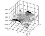
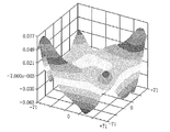
- FIG. 3 shows the result of measuring the surface shape of the main surface of the mask blank substrate according to Example 1 of the present invention.
- FIG. 4 is a schematic enlarged cross-sectional view of the main part of the mask blank substrate according to Example 1 of the present invention.
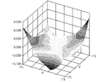
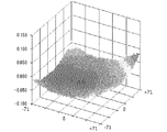
- FIG. 5 shows the result of measuring the surface shape of the main surface of the mask blank substrate according to Comparative Example 1 of the present invention.
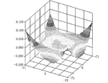
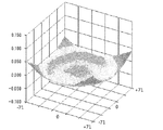
- FIG. 6 shows the result of measuring the surface shape of the main surface of the mask blank substrate according to Comparative Example 2 of the present invention.
- FIG. 7 shows the result of measuring the surface shape of the main surface of the mask blank substrate according to Comparative Example 3 of the present invention.
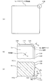
- FIG. 8 is a schematic view for explaining a substrate mark of a mask blank substrate related to the present invention, (a) shows a plan view, (b) shows an enlarged view of E part, (C) shows an FF cross-sectional view.
- FIG. 9 is a schematic view of a main part of a mask blank substrate for explaining the problem of the present invention.
- FIG. 9A is an enlarged cross-sectional view when an ultra-precision polishing process is started, and FIG. Shows an enlarged cross-sectional view after finishing the ultra-precision polishing process.
- FIG. 10 shows the result of measuring the surface shape of the main surface of the mask blank substrate according to Example 2 of the present invention.
- FIG. 11 shows the result of measuring the surface shape of the main surface of the mask blank substrate according to Example 3 of the present invention.
- FIG. 8 is a schematic view for explaining a substrate mark of a mask blank substrate related to the present invention, (a) shows a plan view, (b) shows an enlarged view of E part, (C) shows an FF cross-sectional view.
- a mask blank substrate 101 shown in FIG. 8 is an example of a mask blank substrate having a rectangular shape on a plane. Here, the rectangular shape includes not only a rectangular shape but also a square shape.
- an R surface 102 is formed at a corner formed by two adjacent side surfaces 110, and between the main surfaces 111 and 112 and the side surface 110 (including the R surface 102).
- a chamfered surface 103 is formed.
- a substrate mark 104 is formed at a corner portion on the back side main surface 112 (a main surface opposite to the main surface on which a thin film for forming a transfer pattern is formed).
- the material of the mask blank substrate 101 is not particularly limited as long as it is used as a mask blank.
- synthetic quartz glass, borosilicate glass, aluminosilicate glass, aluminoborosilicate glass, soda lime glass In addition to the alkali-free glass, low thermal expansion glass such as SiO 2 —TiO 2 glass is also used for the substrate used for the reflective mask in particular.
- a mask blank substrate 101 having a side length of about 152 mm (6 inches) and a thickness of about 6.35 mm (0.25 inches) is widely used.
- the shape and thickness of the mask blank substrate 101 are not particularly limited.
- the R surfaces 102 are curved surfaces formed at the four corners of the mask blank substrate 101, and the radius of curvature is usually 2.5 ⁇ 0.5 mm.
- an annular chamfered surface 103 is formed between each of the peripheral surfaces of the main surfaces 111 and 112 and the side surface 110 (including the R surface 102).
- the chamfered surface 103 is an inclined surface (also referred to as a C surface) inclined by about 45 °, and usually has a chamfering width of 0.4 to 0.6 mm.
- the mask blank substrate 101 has the substrate mark 104 formed on the main surface 112 on the back side, but is not limited thereto.
- the substrate mark 104 is formed at the upper right corner in FIG. 8, and includes a main surface 112, an R surface 102, a side surface 110 following the R surface 102, and the main surface 112 and the side surface 110 (including the R surface 102).
- An oblique cross section (one oblique cross section) formed on the chamfered surface 103 therebetween is formed.
- the substrate mark 104 includes a linear boundary 141 intersecting with the main surface 112 (that is, a boundary 141 between the substrate mark 104 and the main surface 112) and a linear boundary intersecting with the R surface 102 (that is, the substrate mark). 104 and the R surface 102).
- a distance W 0 from the boundary 141 between the substrate mark 104 and the main surface 112 to the boundary between the substrate mark 104 and the R surface 102 (this distance W 0 is a distance on a virtual plane including the vicinity of the central portion of the main surface 112.
- the maximum value of the distance from an arbitrary point on the boundary 141 to the boundary between the substrate mark 104 and the R plane 102 in the direction orthogonal to the line of the boundary 141 is approximately).
- the maximum height H 0 in the side surface direction to the boundary between the substrate mark 104 and the R surface 102 with reference to a virtual plane including the vicinity of the central portion of the main surface 112 is about 1 mm in this example,
- the inclination angle ⁇ 0 of the substrate mark 104 with respect to the main surface 112 is about 25 °.
- a substrate mark 104 is formed at one corner.
- the substrate mark 104 is formed at a plurality of corners according to the material, and the material is identified based on the number and position of the formed substrate mark 104.
- the substrate mark 104 is usually formed by a grinding process using a diamond grindstone or the like, and is further subjected to a mirror finish so that dirt is not attached in a cleaning process or the like.
- FIG. 9 is a schematic view of the main part of the mask blank substrate, in which (a) shows an enlarged cross-sectional view of the main surfaces 111 and 112 when the ultraprecision polishing process is started, and (b) The expanded sectional view after complete
- polishing process is shown.
- the mask blank substrate 101 is sandwiched between a pair of opposing polishing pads 21 provided in a double-side polishing apparatus.
- a polishing liquid (not shown) containing colloidal silica is supplied to the polishing pad 21, and a predetermined pressure is applied in the vertical direction.
- the polishing pad 21 is usually an ultra-soft polisher (suede type).
- the mask blank substrate 101 sandwiched between the polishing pads 21 revolves and rotates while being held by a carrier (not shown), and the main surfaces 111 and 112 are simultaneously polished.
- the main surface 112 presses the lower polishing pad 21, so that the main surface 112 is outside the boundary 141 and below the substrate mark 104 that is not pressed by the substrate 101 of the polishing pad 21.
- the convex part 211 which consists of the polishing pad 21 shown in FIG.
- the boundary 141 where the stress is concentrated comes into contact with the convex portion 211, and the boundary 141 tries to get over the convex portion 211. Presumed to be polished. For this reason, the vicinity of the boundary 141 of the main surface 112 is in a state of being excessively polished as compared with other regions of the main surface 112.
- the mask blank substrate 101 polished for a predetermined time has a large edge sagging portion 106 in the vicinity of the R surface 102 of the main surface 112 on which the substrate mark 104 is formed. End up.
- the raised portion 105 is formed conversely.
- the region where the edge sag portion 106 and the raised portion 105 were formed substantially corresponded, and h 01 ⁇ h 02 .
- FIG. 1A and 1B are schematic views for explaining a substrate mark of a mask blank substrate according to a first embodiment of the present invention.
- FIG. 1A is a plan view
- FIG. (C) shows a BB cross-sectional view.
- a mask blank substrate 1 of the present embodiment has a configuration in which a substrate mark 4 having an oblique cross section is formed.
- the mask blank substrate 1 is different from the mask blank substrate 101 described above in that a substrate mark 4 having a different cross-sectional shape and size is formed instead of the substrate mark 104.
- the other configuration of the present embodiment is almost the same as that of the mask blank substrate 101. Therefore, in FIG. 1, the same components as those in FIG. 8 are denoted by the same reference numerals, and detailed description thereof is omitted.
- the substrate mark 4 is formed at the upper right corner in substantially the same manner as the substrate mark 104.
- the substrate mark 4 includes a linear boundary 41 intersecting with the main surface 112 (that is, a boundary 41 between the substrate mark 4 and the main surface 112) and a linear boundary intersecting with the R surface 102 (that is, the substrate mark). 4 and the R surface 102).
- this distance W 1 is a distance on a virtual plane including the vicinity of the central portion of the main surface 112.
- the maximum value of the distance from an arbitrary point on the boundary 41 to the boundary between the substrate mark 4 and the R plane 102 in the direction orthogonal to the line of the boundary 41 is less than 1.5 mm. It is.
- the distance W 1 is preferably 1.4mm or less.
- the maximum value H 1 of the height in the side surface direction up to the boundary between the substrate mark 4 and the R surface 102 with reference to the virtual plane including the vicinity of the central portion of the main surface 112 is not particularly limited.
- H 1 is preferably set to 1.2 mm or more, and more preferably 1.5 mm or more.
- the maximum height H 1 of the substrate marks 4 in the case of the mask blank substrate with a thickness of 6.35 mm it is desirable to exceed 18% of the thickness, it is more desirable that 24% or more.
- the surface shape of the substrate mark 4 is preferably a shape (axisymmetric shape) having high symmetry with respect to a diagonal line B passing through the R surface 102 of the substrate.
- both the main surfaces 111 and 112 are required to have a high level of surface roughness. For this reason, it is necessary to perform a polishing process on the main surface of the substrate after the grinding process.
- the edge sag advances from the boundary 41 toward the center of the main surface, and the edge sag portion 106 is formed after the polishing process ( (See FIG. 9B). If the distance W 1 is set to 1.5 mm or more, the edge sag portion 106 formed after the polishing process proceeds too far toward the center of the main surface 112.
- the raised portion 105 is formed on the main surface 111 so as to correspond to the edge sag portion 106, an adverse effect on the flatness of the main surface 111 is increased.
- the distance W 1 is less than 1.5 mm, the advance of the edge sag portion 106 toward the center side of the main surface 112 and further the progress of the ridge 105 toward the center side of the main surface 111 are minimized.
- the flatness of the main surface 111 after the polishing process can be set to a predetermined value or less.
- the mask blank substrate of the present invention includes any of a light transmissive transfer mask used in light transmissive lithography and a mask blank serving as an original plate, a reflective mask used in reflective lithography and a reflective mask blank serving as an original plate. It is also applicable to.
- a substrate used for a reflective mask is required to have a very high level of flatness and surface roughness of the main surface. For example, the flatness in a corner area of 132 mm ⁇ 132 mm with respect to the center of the main surface (a position on the main surface 111 that is moved inward by 10 mm from the position of the side surface 110 and a region closer to the center than that position) It is necessary to be 0.05 ⁇ m or less. Further, the surface roughness of the main surface needs to be not more than 0.15 nm in terms of the root-mean-square roughness Rq in a 10 ⁇ m ⁇ 10 ⁇ m square area.
- the substrate after the polishing step often cannot satisfy the required high flatness.
- a substrate satisfying the above-mentioned flatness is manufactured by measuring the main surface shape of the substrate after the polishing step and locally processing the convex portion of the main surface.
- the longer the time for performing the local processing the greater the degree of deterioration of the surface roughness of the main surface that is improved by the polishing process.
- it is important to define the shape of the substrate mark so that the flatness of the substrate after the polishing step can satisfy the above numerical values, or even if not, the flatness of the substrate is closer to the standard.
- a reflective mask is provided with a conductive film made of a conductive material on a main surface 112 opposite to a main surface 111 on which a multilayer reflective film is formed.
- the entire surface of the conductive film is fixed by electrostatic chucking on a flat chuck stage.
- the main surface 112 is also required to have a high flatness equal to or higher than the predetermined value, and it is important to define the shape of the substrate mark that suppresses the progress toward the center of the edge sag portion of the main surface 112. is there.
- the inclination angle ⁇ 1 of the substrate mark 4 with respect to the main surface 112 is preferably greater than 45 ° and less than 90 °. More preferably, the inclination angle theta 1 of the may be less than 60 ° or 90 °.
- the distance W 1 of the may be less than 1.0 mm.
- the progress of the edge sag portion 106 toward the center of the main surface 112 and further the progress of the raised portion 105 toward the center of the main surface 111 can be further minimized, and the main surfaces 111 and 112 can be minimized.
- the time required for local processing can be reduced even if the range in which the flatness of the film can be made below the predetermined value is expanded (for example, a 142 mm ⁇ 142 mm in-corner region with the center of the main surface as a reference). Can do.
- the boundary 41 of the substrate mark 4 is preferably substantially orthogonal to the diagonal line B passing through the R surface 102 of the substrate. By configuring in this way, the distribution of the edge sag portion 106 of the main surface 112 after the polishing process can tend to have higher line symmetry with respect to the diagonal B.
- the mask blank substrate 1 on which the substrate mark 4a and the substrate mark 4b are formed can further improve the flatness.
- Each dimension, such as a substrate mark 4 is not limited to the above dimensions, distance W 1 as long as they satisfy the condition that it is less than 1.5 mm, is set to an appropriate size.
- the distance W 1 of the substrate mark 4 in this first embodiment regardless of the length of one side of the substrate forming the substrate mark 4 (one side is greater than 6 inches, e.g. A substrate having a rectangular main surface having a length of 8 inches or more, a substrate having a rectangular main surface having a side smaller than 6 inches, for example, a length of 5 inches or less)
- the center side region a region closer to the center than the position
- the method for manufacturing a mask blank substrate according to the present embodiment includes a substrate mark forming step for forming a substrate mark 4 having an oblique section on the mask blank substrate 1 and both surfaces of the mask blank substrate 1 including abrasive grains.
- the method includes a polishing step of polishing using a polishing liquid.
- the substrate mark forming process First, the substrate mark forming process, the mask blank substrate 1, the distance W 1 of the to less than 1.5 mm, the substrate mark 4 is formed (see FIG. 1).
- the substrate mark 4 is usually formed by grinding using a diamond grindstone or the like, and is further subjected to mirror finishing so that dirt is not attached in a cleaning process or the like.
- the polishing step the mask blank substrate 1 on which the substrate mark 4 is formed is subjected to polishing using a double-side polishing apparatus (for example, the double-side polishing apparatus described in Patent Document 1).
- the polishing process usually includes rough polishing process and precision polishing process using a polishing liquid containing cerium oxide, and super-precision polishing process using a polishing liquid containing colloidal silica. Processing is applied.
- the above double-side polishing apparatus is not illustrated, it is a planetary gear system, and is engaged with the sun gear, the internal gear arranged concentrically on the outer side, the sun gear and the internal gear, and the sun gear and the internal gear.
- a carrier that revolves and rotates according to the rotation of the gear, an upper surface plate and a lower surface plate that can hold the mask blank substrate 1 held by the carrier, to which a polishing pad is attached, and an upper surface plate and a lower surface plate,
- a polishing liquid supply section for supplying a polishing liquid is provided between the two.
- a mask blank substrate 1 held by a carrier is sandwiched between an upper surface plate and a lower surface plate, and a polishing liquid is supplied between the polishing pad of the upper and lower surface plates and the mask blank substrate 1.
- the carrier revolves and rotates in accordance with the rotation of the sun gear and the internal gear, and simultaneously polishes both the main surfaces 111 and 112 of the mask blank substrate 1.
- the mask blank substrate 1 that has been subjected to polishing processing (particularly, ultra-precision polishing processing) is formed with the raised portion 105 and the edge sag portion 106 as described above because the substrate mark 4 is formed under the above conditions. It is possible to effectively eliminate such adverse effects (see FIG. 9) and achieve high flatness.
- the polishing process of this embodiment (this process corresponds to a preparation process in Patent Document 2). After that, there are cases where an uneven shape measuring step and a flatness control step are performed. Even in such a case, the polishing process of the present embodiment capable of realizing high flatness is effective, and reduces the work load (load for performing local polishing) in the flatness control process. And productivity can be improved.
- the polishing process is performed using a planetary gear type double-side polishing apparatus, but the polishing apparatus is not limited to this. For example, another type of double-side polishing apparatus or single-side polishing is performed. You may use the single-side polish apparatus which performs.
- the adverse effect on the flatness due to the substrate mark 4 having an oblique cross section is eliminated in the polishing process. Flatness can be improved.
- FIG. 2A and 2B are schematic views for explaining a substrate mark of a mask blank substrate according to a second embodiment of the present invention.
- FIG. 2A is a plan view
- FIG. (C) shows a DD cross-sectional view.
- the mask blank substrate 1 c of this embodiment is different from the mask blank substrate 1 described above in that a substrate mark 4 c is formed instead of the substrate mark 4.
- the other configuration of the present embodiment is almost the same as that of the mask blank substrate 1. Therefore, in FIG. 2, the same components as those in FIG. 1 are denoted by the same reference numerals, and detailed description thereof is omitted.
- the substrate mark 4c is also formed at the upper right corner in the same manner as the substrate mark 4 in the case of FIG. 2, but the chamfered surface 103 between the main surface 112 and the side surface 110 (including the R surface 102), and the R surface 102 is an oblique cross section (one oblique cross section) formed over the area 102.
- the substrate mark 4c includes a curved boundary 41c that intersects the chamfered surface 103 (that is, a boundary 41c between the substrate mark 4c and the chamfered surface 103), and a linear boundary that intersects the R surface 102 (that is, the substrate mark). 4c and the R surface 102), and the boundary 41c is formed so as to be located on the outer peripheral side with respect to the boundary between the main surface 112 and the chamfered surface 103.
- this distance W 2 is a virtual plane including the vicinity of the central portion of the main surface 112. This is the maximum value of the distance from any point on the boundary 41c to the boundary between the substrate mark 4c and the R plane 102 in the direction perpendicular to the line (tangent) of the boundary 41c. Is about 0.3 mm.
- the maximum height H 2 in the side surface direction up to the boundary between the substrate mark 4c and the R surface 102 with reference to a virtual plane including the vicinity of the central portion of the main surface 112 is about 1.1 mm, and the main surface inclination angle theta 2 of the substrate marks 4c for 112 is about 75 °. Accordingly, the substrate mark 4c satisfies the conditions such inclination angle theta 2 is greater than 90 ° than 45 °. That is, the maximum H 2 of the substrate mark 4c according to this embodiment is 17% or more of the thickness (6.35 mm).
- the substrate mark 4c is formed so as to be located on the boundary between the main surface 112 and the chamfered surface 103 or on the outer peripheral side with respect to the boundary between the main surface 112 and the chamfered surface 103.
- the difference from the other corners where the substrate mark 4c is not formed is substantially eliminated. be able to.
- the difference between the corner portions of the main surface 112 related to the edge sag portion 106 can be eliminated, the difference between the corner portions related to the raised portion 105 generated on the opposite main surface 111 is also substantially eliminated. Can do.
- both the main surfaces 111 and 112 after the polishing step can be set to a predetermined value or more by the above effect. Since the difference between the corners related to the raised portion 105 of the main surface 111 and the difference between the corners related to the edge sag portion 106 of the main surface 112 are substantially eliminated, both the main surfaces 111 and 112 are linear. A surface shape having high symmetry and point symmetry can be obtained.
- the substrate mark 4c has the effects as described above, by setting the conditions as shown in the second embodiment, regardless of the length of one side of the substrate on which the substrate mark 4c is formed (one side is 6 inches).
- a substrate having a rectangular main surface with a length of 8 inches or more, or a rectangular main surface with a side length of less than 6 inches, for example, 5 inches or less In the main surface 111 of the substrate, a position moved to the center side of the main surface 111 by 10 mm from the position of the side surface 110 viewed from the main surface 111 side, and a region closer to the center than the position (hereinafter referred to as the center)
- the flatness can be set to a predetermined value or more.
- the flatness of a predetermined value or more can be achieved on the main surface 112 on the opposite side.
- both the main surfaces 111 and 112 can have a surface shape with high line symmetry and point symmetry.
- the processing time is required even when the local processing is performed on the convex portions of the main surfaces 111 and 112. Can be greatly shortened. Furthermore, it is possible to suppress deterioration of the surface roughness of the main surfaces 111 and 112 due to local processing.
- the substrate mark 4 can be a surface extending in the thickness direction, and the visibility is improved. be able to. More preferably, the inclination angle theta 2 of the may be less than 60 ° or 90 °.
- the manufacturing method of the mask blank substrate 1c differs from the manufacturing method of the above-described embodiment in that a substrate mark 4c having a different inclination angle is formed instead of the substrate mark 4.
- the manufacturing method of the present embodiment is substantially the same as the manufacturing method of the above-described embodiment, and the flatness of the mask blank substrate 1c can be further improved.
- the mask blank substrate 1c and the manufacturing method thereof according to the present embodiment substantially the same effects as those of the above-described embodiment can be obtained, and the adverse effect on the flatness caused by the substrate mark 4c can be almost certainly eliminated. In addition, it is possible to realize a further excellent high flatness of the mask blank substrate 1c.
- the mask blank of this embodiment is configured to include a thin film for forming a transfer pattern on the main surface 111 of the mask blank substrate 1, 1c of each of the first and second embodiments described above.
- This mask blank can achieve excellent high flatness by using the mask blank substrates 1 and 1c.
- a thin film formed on a light transmissive mask blank is a thin film that causes an optical change with respect to exposure light (light emitted from an exposure light source) used when transferring to a transfer target.
- a light shielding film For example, a light shielding film , A halftone phase shift film, and a light semi-transmissive film.
- the light-shielding film has an optical density (for example, optical density of 3.0 or more, 2.5 or more, etc.) of a predetermined value or higher with respect to exposure light, and has a function of shielding exposure light.
- a mask blank using a light-shielding film as a thin film for forming a transfer pattern is mainly used when a binary transfer mask or an engraved Levenson mask is manufactured.
- the light shielding film is not limited to a single layer structure, and includes a structure in which a light shielding layer mainly having a light shielding function and an antireflection layer mainly having a function of reducing the reflectance with respect to exposure light are laminated.
- Examples of materials applicable to the light shielding film include a material containing Cr, a material containing a transition metal and silicon, and a material containing Ta.
- the material containing Cr include Cr metal or a Cr compound containing one or more elements selected from N, C, O, F, and H in Cr.
- the material containing transition metal and silicon include transition metal silicide composed of transition metal and silicon, or transition metal silicide compound containing one or more elements selected from C, N, O, and B in addition to transition metal silicide. can give.
- the transition metal is preferably a metal or alloy selected from Mo, Ta, Hf, Zr, Cr, Ti, V, Ni, Fe, Nb, W, Ru, Rh, Pd, and Ag.
- the material containing Ta include Ta metal and Ta compounds containing one or more elements selected from B, C, N, and O in Ta.
- the halftone phase shift film is a film that transmits the exposure light with a predetermined transmittance and generates a predetermined phase difference with respect to the exposure light transmitted through the light transmitting portion where the film is not formed. It has a function of causing a phase shift effect between the exposure light transmitted through the film and the exposure light transmitted through the light transmission portion.
- a mask blank using a halftone phase shift film as a thin film for forming a transfer pattern is mainly used for producing a halftone phase shift mask.
- Examples of the material applicable to the halftone phase shift film include a material containing a transition metal and silicon.
- Examples of the material containing a transition metal and silicon include a transition metal silicide compound containing one or more elements selected from C, N, O, and B in addition to a transition metal silicide composed of a transition metal and silicon.
- the transition metal is the same as that of the light shielding film.
- the light semi-transmissive film transmits the exposure light with a predetermined transmittance, but has a phase difference that does not substantially cause a phase shift effect between the exposure light transmitted through the film and the exposure light transmitted through the light transmission part. It is a film that does not cause phase difference.
- a mask blank using a light semi-transmissive film as a thin film for forming a transfer pattern is mainly used when an enhancer type phase shift mask is manufactured.
- a material applicable to the light semi-transmissive film a material containing a transition metal and silicon is preferable like the halftone phase shift film.
- the light transmissive mask blank has g-line (wavelength: 436 nm), i-line (wavelength: 365 nm), KrF (wavelength: 246 nm), ArF (wavelength: 193 nm), F2 (wavelength: 157 nm) as an exposure light source. Is used. Further, the light shielding film, the halftone phase shift film, and the light semi-transmissive film can be formed by a sputtering method such as DC sputtering, RF sputtering, or ion beam sputtering.
- a sputtering method such as DC sputtering, RF sputtering, or ion beam sputtering.
- the manufacturing method of the mask blank of this embodiment is enumerated above on the mask blank substrates 1 and 1c obtained by the manufacturing method of the mask blank substrate of the first and second embodiments described above.
- This is a method for forming a thin film to be a transferred pattern.
- excellent high flatness can be realized by using the mask blank substrates 1 and 1c.
- a mask blank having excellent high flatness can be provided.
- the reflective mask blank of this embodiment includes a multilayer reflective film that reflects exposure light at a high reflectance on the main surface 111 of the mask blank substrate 1, 1c of each of the first and second embodiments described above.
- the multilayer reflection film has a function of absorbing exposure light and includes at least an absorber film that is a thin film for forming a transfer pattern.
- the reflective mask blank of this embodiment includes a configuration in which a protective film and a buffer film are provided between the multilayer reflective film and the absorber film.
- the reflective mask blank of this embodiment also includes a configuration in which a conductive film having conductivity is provided on the main surface 112 opposite to the main surface 111 on which a multilayer reflective film or the like is formed.
- the multilayer reflective film has one cycle of a stack of a low refractive index layer made of a material having a low refractive index with respect to exposure light and a high refractive index layer made of a material with a high refractive index, and this is a plurality of cycles (at least 20 cycles or more, (Preferably 40 cycles or more).
- EUV Extreme Ultra Violet
- a Si layer is preferable for the low refractive index layer
- Mo is preferable for the high refractive index layer.
- the absorber film is a thin film for forming a transfer pattern and is required to have high absorption performance with respect to exposure light.
- a material containing Ta is suitable as a material for forming the absorber film.
- Ta metal, Ta and B, Hf, Zr, Nb, Pt, W, Au, Re, Os, and Ta compound consisting of one or more elements selected from Si, Ta metal and Ta compound examples thereof include materials containing one or more elements selected from N, O, and C.
- the protective film protects the multilayer reflective film during dry etching when a transfer pattern is formed on the absorber film, and the multilayer from the cleaning process performed on the reflective mask during and after the reflective mask manufacturing process. It mainly has a role of protecting the reflective film.
- the material applicable to the protective film include a material containing Ru and a material containing Si.
- the materials containing Ru, Ru metal, an alloy with one or more metals selected from Ru, Nb, Zr, Mo, Ti, and La are preferable.
- the buffer film is made of a material resistant to the etching gas used when dry-etching the absorber film, but after the transfer pattern is formed on the absorber film, dry etching using the absorber pattern as a mask Is patterned.
- the material for forming the buffer film is not resistant to the etching gas used when dry-etching the buffer film itself. It is required not to do damage.
- the buffer film is preferably a material containing Cr. Specifically, Cr metal or a Cr compound containing one or more elements selected from N, C, O, F, and H in Cr can be used.
- the conductive film is a film required when electrostatically chucking the produced reflective mask on the mask stage of the exposure apparatus when electrostatically chucking the substrate on the rotary stage when forming the multilayer reflective film. In terms of its role, conductivity is required. Suitable materials for this conductive film include materials containing Cr and materials containing Ta. Specifically, the material containing Cr includes Cr metal or Cr compound containing one or more elements selected from N, C, O, F, and H in Cr. In addition, the Ta-containing material includes Ta metal or Ta compound containing one or more elements selected from B, C, N, and O in Ta.
- the multilayer reflective film, absorber film, protective film, buffer film, and conductive film can be formed by a sputtering method such as DC sputtering, RF sputtering, or ion beam sputtering.
- the mask blank substrate is not required to have a high transmittance for exposure light. .
- the substrate is required to be formed of a material having a low thermal expansion coefficient.
- the substrate made of a material having a low thermal expansion coefficient include amorphous glass such as SiO 2 —TiO 2 glass and quartz glass, and crystallized glass on which ⁇ -quartz solid solution is precipitated.
- the reflective mask blank manufacturing method of the present embodiment exposes the mask blank substrates 1, 1c obtained by the mask blank substrate manufacturing methods of the first and second embodiments described above.
- This is a method of forming at least a multilayer reflective film that reflects light with a high reflectance and an absorber film that has a function of absorbing exposure light on the multilayer reflective film and is a thin film for forming a transfer pattern.
- excellent high flatness can be realized by using the mask blank substrates 1 and 1c.
- a mask blank having excellent high flatness can be provided.
- the transfer mask of this embodiment has a configuration in which a transfer pattern is formed on the above-described mask blank thin film. This transfer mask can realize excellent high flatness by using the above-described mask blank.
- the transfer mask manufacturing method of the present embodiment is a method of forming a transfer pattern on the thin film of the mask blank obtained by the mask blank manufacturing method of the above-described embodiment. That is, the transfer mask manufacturing method usually includes a step of preparing a mask blank obtained by the above-described mask blank manufacturing method, and a resist film is formed on the thin film by a spin coating method or the like. A pattern forming process of forming a desired resist pattern by exposing and drawing the transfer pattern and developing, and a thin film pattern forming process of forming a transfer pattern on the thin film by masking the resist pattern and etching the thin film Have.
- the transfer mask manufacturing method excellent high flatness can be realized by using the mask blank substrates 1 and 1c.
- the transfer mask of this embodiment is applied to the binary transfer mask, the digging Levenson phase shift mask, the halftone phase shift mask, the enhancer phase shift mask, and the like.
- the reflective mask of this embodiment has a configuration in which a transfer pattern is formed on the absorber film of the reflective mask blank described above. This reflective mask can realize excellent high flatness by using the above-described reflective mask blank.
- the reflective mask manufacturing method of the present embodiment is a method for forming a transfer pattern on the absorber film of the reflective mask blank obtained by the reflective mask blank manufacturing method of the above-described embodiment. That is, the reflective mask manufacturing method usually includes a step of preparing the reflective mask blank obtained by the above-described reflective mask blank manufacturing method, and a resist film is formed on the absorber film by a spin coat method or the like. Then, a transfer pattern is exposed and drawn on the resist film, and a pattern forming process for forming a desired resist pattern through development processing and the like, and the resist pattern is masked, and the absorber film is removed by etching to form an absorber film. And an absorber pattern forming step for forming a transfer pattern.
- a substrate made of TiO 2 —SiO 2 having a low thermal expansion coefficient, having a substantially square planar shape, a length of about 152 mm (6 inches) on one side, and a thickness of 6.35 mm (0.25 inches) 1c was prepared.
- the R surface 102, the chamfered surface 103, and the substrate mark 4c were formed on the substrate 1c (see FIG. 2).
- the R surface 102 is a curved surface formed at the four corners of the substrate 1c and has a radius of curvature of 2.5 mm.
- the chamfered surface 103 is formed on the periphery of the main surface 111 and the main surface 112, and has a chamfer width of 0.5 mm.
- the substrate 1c has the main surface 111 on the side on which the multilayer reflective film and the absorber film are formed, and the main surface 112 on the side on which the conductive film is formed.
- the substrate mark 4c is formed in the upper right corner and the lower left corner in FIG. 2, and is an oblique cross section obtained by cutting off the R surface 102 and the chamfered surface 103 between the main surface 112 and the side surface 110 (including the R surface 102). (One oblique section).
- the substrate mark 4 c has a curved boundary 41 c that intersects the chamfered surface 103, and is formed so as to be positioned on the outer peripheral side from the boundary between the main surface 112 and the chamfered surface 103.
- this distance W 2 is a distance on a virtual plane including the vicinity of the central portion of the main surface 112.
- the maximum height H 2 in the side surface direction up to the boundary between the substrate mark 4c and the R surface 102 with reference to the virtual plane including the vicinity of the central portion of the main surface 112 is about 1.5 mm, and the main surface the inclination angle theta 2 of the substrate marks 4c for 112 was about 75 °. That is, the maximum value of H 2 height of the substrate mark 4c shown is not less than 23% of the thickness (6.35 mm).
- the substrate mark 4c was formed by grinding using a diamond grindstone or the like, and finished with a mirror finish. Subsequently, the substrate 1c was ground by a double-sided lapping device.
- the substrate 1c on which the substrate mark 4c was formed was subjected to polishing (rough polishing, precision polishing, and ultra-precision polishing) using the above-described double-side polishing apparatus.
- polishing rough polishing, precision polishing, and ultra-precision polishing
- the processing load and polishing time were adjusted as appropriate.
- Polishing liquid Cerium oxide (average particle size 2 to 3 ⁇ m) + water Polishing pad: Hard polisher (urethane pad)
- the substrate 1c was immersed in the cleaning tank (ultrasonic application) in order to remove the abrasive grains adhering to the substrate 1c, and cleaning was performed.
- Polishing liquid Colloidal silica (average particle size 30 to 200 nm) + water Polishing pad: Super soft polisher (suede type)
- the substrate 1c was immersed in a cleaning tank containing a cleaning solution containing hydrofluoric acid and silicic acid (ultrasonic application) to perform cleaning.
- the surface shape (flatness) of the main surface 111 of the cleaned substrate 1c was measured with an optical interference type flatness measuring device (UltraFLAT200M manufactured by Corning TROPEL).
- the measured surface shape distribution of the main surface 111 is shown in FIG.
- the surface shape distribution in FIG. 3 is a 142 mm ⁇ 142 mm in-corner region based on the center of the main surface 111 of the substrate (the same applies to each comparative example hereinafter).
- the flatness in the 132 mm ⁇ 132 mm square region with respect to the center of the main surface 111 of the substrate 1c was about 0.065 ⁇ m, which was a good result. Further, in the surface shape distribution of the main surface 111 in FIG.
- the shapes in the vicinity of the R surface 102 at the four corners of the substrate 1 c are all slightly convex (the raised portions 5 are generated).
- the variation in height of the convex shape between the corners was very small (see FIG. 4).
- the surface shape distribution on the main surface 112 side was measured in the same manner, the shape of the four corners of the substrate 1c in the vicinity of the R surface 102 had some fringed portions 6 between the four corners.
- the variation in the height level of the edge portion 6 was very small.
- the flatness in a 132 mm ⁇ 132 mm in-corner region with respect to the center of the main surface 112 was also good as with the main surface 111.
- both the main surfaces 111 and 112 have a flatness in a corner area of 132 mm ⁇ 132 mm with respect to the center of the main surface 111 (main surface 112) as EUV light.
- the flatness in the 132 mm ⁇ 132 mm in-corner region required for a mask blank substrate for producing a reflective mask blank using exposure light as the exposure light is not satisfied. Therefore, a local processing step was performed in order to satisfy the desired flatness. Specifically, first, based on the data of the surface shape distribution of the main surfaces 111 and 112 measured previously, the position of the convex portion to be locally processed and the required processing amount were calculated in order to satisfy the desired flatness. .
- the substrate 1c was set and information on the position of the convex portion and the required processing amount was input to an MRF processing apparatus that performs local processing using a magnetic fluid, and local processing was performed on the main surfaces 111 and 112.
- the time required for processing can be greatly reduced as compared with the case of a substrate having a conventional substrate mark shape.
- polishing including colloidal silica abrasive grains is used, and the surface roughness is recovered by a double-side polishing apparatus (Rq is 0.15 nm or less). Polishing was performed for a short time. The time required for recovering the surface roughness could be shortened as compared with the case of the substrate having the conventional substrate mark shape. Finally, a predetermined cleaning process or the like was performed to obtain a mask blank substrate 1c that can be used for manufacturing a reflective mask blank.
- a CrN film having a thickness of 30 nm was formed as a conductive film on the main surface 112 of the obtained mask blank substrate 1c by a sputtering method.
- the conductive film was not formed in the outer peripheral region (at least the chamfered surface 103) of the main surface 112.
- the mask blank substrate 1c on which the conductive film was formed was electrostatically chucked on the rotary stage of the ion beam sputtering apparatus, and a Si / Mo multilayer reflective film was formed by ion beam sputtering.
- a protective film made of RuNb was formed to a thickness of 2.5 nm on the Si film of the multilayer reflective film. Further, an absorber film having a laminated structure of a lower layer made of TaN and an upper layer made of TaO was formed on the protective film to obtain a reflective mask blank.
- a resist film for electron beam exposure was formed on the absorber film of the obtained reflective mask blank by spin coating.
- the resist film was subjected to electron beam drawing and development treatment to form a resist pattern having a transfer pattern.
- dry etching with CF 4 gas was performed to form a transfer pattern on the absorber film.
- dry etching with Cl 2 gas was performed using the resist pattern and the upper transfer pattern as a mask to form a transfer pattern in the lower layer of the absorber film.
- the resist pattern was peeled off and a predetermined cleaning process was performed to obtain a reflective mask.
- the obtained reflective mask was fixed to a mask stage of an exposure apparatus with an electrostatic chuck, and exposure transfer using EUV light as exposure light was performed on the resist film on the semiconductor wafer.
- a predetermined development process or the like was performed on the resist film after exposure and transfer, and using this resist film as a mask, dry etching was performed on the thin film on the semiconductor wafer to form a circuit pattern.
- the circuit pattern formed on the semiconductor wafer was observed with a TEM, it was confirmed that the circuit pattern was formed with high accuracy. This result is largely due to the high flatness of the reflective mask substrate 1c used.
- Comparative Example 1 is different from Example 1 in that the substrate mark 104 described above is formed instead of forming the substrate mark 4.
- the processing conditions such as the polishing process of the comparative example are almost the same as those in the first embodiment. Therefore, the detailed description of the same contents as in the first embodiment is omitted.
- the substrate marks 104 are formed at the upper right corner and the lower left corner in FIG. 8, and are the main surface 112, the R surface 102, the two side surfaces 110 following the R surface 102, the main surface 112 and the side surfaces 110 (R surface).
- the oblique section (one oblique section) was cut off from the chamfered surface 103 between the two.
- the substrate mark 104 has a line-shaped boundary 141 intersecting the main surface 112, and the substrate mark 104 is perpendicular to the diagonal line passing through the R plane 102 when viewed from above. Formed. Further, a distance W 0 from the boundary 141 between the substrate mark 104 and the main surface 112 to the boundary between the substrate mark 104 and the R surface 102 (this distance W 0 is a distance on a virtual plane including the vicinity of the central portion of the main surface 112. The maximum value of the distance from an arbitrary point on the boundary 141 to the boundary between the substrate mark 104 and the R surface 102 in the direction orthogonal to the line of the boundary 141) is about 3.0 mm. It was.
- the main surface The inclination angle ⁇ 0 of the substrate mark 104 with respect to 112 was set to about 22 °. That is, the maximum value H 0 of the height is less than 19% with respect to the thickness of the substrate.
- the substrate mark 104 was formed by a grinding process using a diamond grindstone or the like, and finished with a mirror finish. Subsequently, the substrate 101 was ground by a double-sided lapping apparatus.
- the substrate 101 on which the substrate mark 104 is formed is polished using the double-side polishing apparatus (rough polishing processing, precision polishing processing, and ultra-precision polishing processing) as in the first embodiment. ). Subsequently, in order to remove the abrasive grains adhering to the substrate 101 after the ultra-precision polishing step, the glass substrate is immersed in a cleaning tank containing a cleaning solution containing hydrofluoric acid and silicic acid (ultrasonic application) to perform cleaning. went.
- the surface shape (flatness) of the cleaned substrate 101 was measured with an optical interference type flatness measuring device (UltraFLAT200M manufactured by Corning TROPEL).
- the measured surface shape distribution of the main surface 111 is shown in FIG.
- the flatness in a 132 mm ⁇ 132 mm square area with respect to the center of the main surface 111 of the substrate 101 was about 0.168 ⁇ m, which was a rather bad result.
- the shape in the vicinity of the two corners of the R surface 102 where the substrate mark 104 of the substrate 101 is formed is the vicinity of the two corners of the R surface 102 where the substrate mark is not formed.
- the shape is larger and higher (the raised portion 105 is generated).
- the variation in height of the convex shape between the four corners is very large.
- the surface shape distribution on the main surface 112 side was also measured in the same manner.
- the shape near the R surface 102 at the two corners where the substrate mark 104 is formed is compared with the shape near the R surface 102 at the other two corners.
- There was a large margin and the variation in the height level of the marginal portion 106 between the four corners was very large.
- the flatness in a 132 mm ⁇ 132 mm in-corner region with respect to the center of the main surface 112 was not as good as that of the main surface 111.
- the comparative example 2 has the substrate mark 104 formed on all four corners in FIG. 8 and the boundary 141 between the substrate mark 104 and the main surface 112.
- the only difference is that the value H 0 is about 1.1 mm and the inclination angle ⁇ 0 of the substrate mark 104 with respect to the main surface 112 is about 25 °. That is, the maximum value H 0 of the height of the substrate mark 104 in Comparative Example 2 is 17% or more of the thickness of the substrate.
- the surface shape (flatness) of the cleaned substrate 101 was measured with an optical interference type flatness measuring apparatus (UltraFLAT200M manufactured by Corning TROPEL).
- the measured surface shape distribution of the main surface 111 is shown in FIG.
- the flatness in a 132 mm ⁇ 132 mm square area with respect to the center of the main surface 111 of the substrate 101 was about 0.116 ⁇ m.
- the shapes near the R surface 102 at the four corners of the substrate 101 are all convex (the raised portions 105 are generated).
- the height variation of the convex shape was very small.
- the surface shape distribution on the main surface 112 side was also measured in the same manner. However, the shapes near the R surface 102 at the four corners of the substrate 1c all had the fringe portion 106, but the edge between the four corners. The variation in the height level of the drooping portion 106 was very small. However, both the main surfaces 111 and 112 had better flatness in the corner area of 132 mm ⁇ 132 mm than that of Comparative Example 1, but were not as good as those of Example 1.
- the comparative example 3 differs from the comparative example 2 in that the substrate marks 104 are formed only at the upper right corner and the lower left corner in FIG.
- the surface shape (flatness) of the cleaned substrate 101 was measured with an optical interference type flatness measuring device (UltraFLAT200M manufactured by Corning TROPEL).
- the measured surface shape distribution of the main surface 111 is shown in FIG.
- the flatness in a 132 mm ⁇ 132 mm square area with respect to the center of the main surface 111 of the substrate 101 was about 0.111 ⁇ m.
- the shape in the vicinity of the two corners of the R surface 102 where the substrate mark 104 of the substrate 101 is formed is the vicinity of the two corners of the R surface 102 where the substrate mark is not formed.
- the shape is larger and higher (the raised portion 105 is generated).
- the surface shape distribution on the main surface 112 side was also measured in the same manner.
- the shape near the R surface 102 at the two corners where the substrate mark 104 is formed is compared with the shape near the R surface 102 at the other two corners.
- the main surfaces 111 and 112 had better flatness in the 132 mm ⁇ 132 mm in-corner region than Comparative Example 1, the results were not as good as those of Example 1.
- the distance W 1 from the boundary 41 between the substrate mark 4 and the main surface 112 to the boundary between the substrate mark 4 and the R surface 102 is about 0.9 mm, and the main surface 112
- the maximum value H 1 of the height in the side surface direction up to the boundary between the substrate mark 4 and the R surface 102 with reference to the virtual plane including the vicinity of the central portion of the substrate mark 4 is about 2.0 mm, and the substrate mark 4 with respect to the main surface 112 different angle of inclination theta 1, only in that the approximately 66 °. That is, the maximum value H 1 of the height of the substrate mark 4 is 31% or more.
- the surface shape (flatness) of the cleaned substrate 1 was measured with an optical interference type flatness measuring device (UltraFLAT200M manufactured by Corning TROPEL).
- the measured surface shape distribution of the main surface 111 is shown in FIG.
- the flatness in a 132 mm ⁇ 132 mm square area with respect to the center of the main surface 111 of the substrate 1 was about 0.075 ⁇ m.
- the shapes in the vicinity of the R surface 102 at the four corners of the substrate 1 are somewhat convex, but the height of the convex shape is between the four corners. The variation was very small.
- the surface shape distribution on the main surface 112 side was also measured in the same manner. However, the shapes near the R surface 102 at the four corners of the substrate 1 were somewhat edged, but the edge between the four corners The variation in the height level of the nose was very small. Further, the flatness in a 132 mm ⁇ 132 mm in-corner region with respect to the center of the main surface 112 was also good as with the main surface 111.
- both the main surfaces 111 and 112 have a flatness in a corner area of 132 mm ⁇ 132 mm with respect to the center of the main surface 111 (main surface 112) as EUV light.
- the flatness in the 132 mm ⁇ 132 mm in-corner region required for a mask blank substrate for producing a reflective mask blank using exposure light as the exposure light is not satisfied. Therefore, in order to satisfy the desired flatness, a local processing step was performed in the same procedure as in Example 1. The time required for the local processing can be greatly shortened as compared with the case of the substrate having the conventional substrate mark shape.
- the reflective mask blank of Example 2 was obtained by the same procedure as in Example 1 using the obtained mask blank substrate 1. Furthermore, using the obtained reflective mask blank, a reflective mask of Example 2 was obtained by the same procedure as in Example 1.
- the obtained reflective mask of Example 2 was fixed to the mask stage of the exposure apparatus with an electrostatic chuck, and exposure transfer using EUV light as exposure light was performed on the resist film on the semiconductor wafer.
- a predetermined development process or the like was performed on the resist film after exposure and transfer, and using this resist film as a mask, dry etching was performed on the thin film on the semiconductor wafer to form a circuit pattern.
- the circuit pattern formed on the semiconductor wafer was observed with a TEM, it was confirmed that the circuit pattern was formed with high accuracy. This result is largely due to the high flatness of the substrate 1 of the reflective mask used.
- the distance W 1 from the boundary 41 between the substrate mark 4 and the main surface 112 to the boundary between the substrate mark 4 and the R surface 102 is about 1.4 mm, compared to the first embodiment.
- the maximum value H 1 of the height in the side surface direction up to the boundary between the substrate mark 4 and the R surface 102 with respect to the virtual plane including the vicinity of the center of the substrate mark 4 is about 1.5 mm, and the substrate mark 4 with respect to the main surface 112 different angle of inclination theta 1, only in that the approximately 47 °.
- the maximum value H 1 height of the substrate mark 4 according to Example 3 is 23% or more.
- the surface shape (flatness) of the cleaned substrate 1 was measured with an optical interference type flatness measuring device (UltraFLAT200M manufactured by Corning TROPEL).
- the measured surface shape distribution of the main surface 111 is shown in FIG.
- the flatness in a 132 mm ⁇ 132 mm square area with respect to the center of the main surface 111 of the substrate 1 was about 0.080 ⁇ m.
- the shapes in the vicinity of the R surface 102 at the four corners of the substrate 1 are somewhat convex, but the height of the convex shape is between the four corners. The variation was very small.
- the surface shape distribution on the main surface 112 side was also measured in the same manner. However, the shapes near the R surface 102 at the four corners of the substrate 1 were somewhat edged, but the edge between the four corners The variation in the height level of the nose was very small. Further, the flatness in a 132 mm ⁇ 132 mm in-corner region with respect to the center of the main surface 112 was also good as with the main surface 111.
- both the main surfaces 111 and 112 have a flatness in a corner area of 132 mm ⁇ 132 mm with respect to the center of the main surface 111 (main surface 112) as EUV light.
- the flatness in the 132 mm ⁇ 132 mm in-corner region required for a mask blank substrate for producing a reflective mask blank using exposure light as the exposure light is not satisfied. Therefore, in order to satisfy the desired flatness, a local processing step was performed in the same procedure as in Example 1. The time required for the local processing can be greatly shortened as compared with the case of the substrate having the conventional substrate mark shape.
- the reflective mask blank of Example 3 was obtained by the same procedure as in Example 1 using the obtained mask blank substrate 1. Further, using the obtained reflective mask blank, a reflective mask of Example 3 was obtained by the same procedure as in Example 1.
- the obtained reflective mask of Example 3 was fixed to the mask stage of the exposure apparatus with an electrostatic chuck, and exposure transfer using EUV light as exposure light was performed on the resist film on the semiconductor wafer. A predetermined development process or the like was performed on the resist film after exposure and transfer, and using this resist film as a mask, dry etching was performed on the thin film on the semiconductor wafer to form a circuit pattern.
- the circuit pattern formed on the semiconductor wafer was observed with a TEM, it was confirmed that the circuit pattern was formed with high accuracy. This result is largely due to the high flatness of the substrate 1 of the reflective mask used.
- the mask blank substrate, the mask blank, the reflective mask blank, the transfer mask, the reflective mask, and the manufacturing method of the mask blank according to the present invention have been described with reference to the preferred embodiments.
- the mask blank according to the present invention has been described.
- Substrate, mask blank, reflective mask blank, transfer mask, reflective mask, and manufacturing method thereof are not limited to the above-described embodiment, and various modifications can be made within the scope of the present invention. It goes without saying that it is possible.
- the mask blank substrates 1 and 1c are formed with the substrate marks 4 and 4c having one oblique section at one corner, but the present invention is not limited to this.
- a substrate mark having two or more oblique sections may be formed at one corner, and may be used in combination with a film mark or the like. Thereby, identification ability can be improved. Furthermore, in the above-described embodiments and examples, a square mask blank substrate having a side length of 152 mm and a thickness of 6.35 mm has been described, but the present invention is not limited to this, and the rectangular mask blank substrate is also not limited thereto. The same applies.
Landscapes
- Physics & Mathematics (AREA)
- General Physics & Mathematics (AREA)
- Engineering & Computer Science (AREA)
- Condensed Matter Physics & Semiconductors (AREA)
- Manufacturing & Machinery (AREA)
- Computer Hardware Design (AREA)
- Microelectronics & Electronic Packaging (AREA)
- Power Engineering (AREA)
- Preparing Plates And Mask In Photomechanical Process (AREA)
- Exposure And Positioning Against Photoresist Photosensitive Materials (AREA)
- Exposure Of Semiconductors, Excluding Electron Or Ion Beam Exposure (AREA)
- Surface Treatment Of Glass (AREA)
Abstract
Priority Applications (2)
| Application Number | Priority Date | Filing Date | Title |
|---|---|---|---|
| KR1020137031095A KR101874504B1 (ko) | 2011-05-19 | 2012-05-15 | 마스크 블랭크용 기판, 마스크 블랭크, 반사형 마스크 블랭크, 전사 마스크, 및 반사형 마스크, 그리고 그들의 제조방법 |
| US14/118,479 US9400421B2 (en) | 2011-05-19 | 2012-05-15 | Mask blank substrate, mask blank, reflective mask blank, transfer mask, reflective mask, and methods of manufacturing the same |
Applications Claiming Priority (2)
| Application Number | Priority Date | Filing Date | Title |
|---|---|---|---|
| JP2011-112185 | 2011-05-19 | ||
| JP2011112185 | 2011-05-19 |
Publications (1)
| Publication Number | Publication Date |
|---|---|
| WO2012157629A1 true WO2012157629A1 (fr) | 2012-11-22 |
Family
ID=47176946
Family Applications (1)
| Application Number | Title | Priority Date | Filing Date |
|---|---|---|---|
| PCT/JP2012/062373 WO2012157629A1 (fr) | 2011-05-19 | 2012-05-15 | Substrat d'ébauche de masque, ébauche de masque, ébauche de masque réfléchissant, masque de transfert, masque réfléchissant et procédé de fabrication associé |
Country Status (5)
| Country | Link |
|---|---|
| US (1) | US9400421B2 (fr) |
| JP (2) | JP5951352B2 (fr) |
| KR (1) | KR101874504B1 (fr) |
| TW (2) | TWI610124B (fr) |
| WO (1) | WO2012157629A1 (fr) |
Families Citing this family (8)
| Publication number | Priority date | Publication date | Assignee | Title |
|---|---|---|---|---|
| JP6055732B2 (ja) * | 2013-07-26 | 2016-12-27 | Hoya株式会社 | マスクブランク用基板、マスクブランク、およびそれらの製造方法、並びにインプリントモールドの製造方法 |
| EP3043375B1 (fr) * | 2013-09-06 | 2023-10-11 | Toppan Photomask Co., Ltd. | Photomasque réfléchissant et son procédé de production |
| JP6384303B2 (ja) * | 2014-12-10 | 2018-09-05 | Agc株式会社 | ガラス基板の研磨方法 |
| JP2017040900A (ja) * | 2015-08-18 | 2017-02-23 | 旭硝子株式会社 | マスクブランク用の基板の製造方法、マスクブランク用の基板、マスクブランク、およびフォトマスク |
| TWI680347B (zh) * | 2015-12-29 | 2019-12-21 | 日商Hoya股份有限公司 | 光罩基板、光罩基底、光罩、光罩基板之製造方法、光罩之製造方法、及顯示裝置之製造方法 |
| WO2018020994A1 (fr) * | 2016-07-27 | 2018-02-01 | Hoya株式会社 | Procédé de fabrication de substrat d'ébauche de masque, procédé de fabrication d'ébauche de masque, procédé de fabrication de masque de transfert, procédé de fabrication de dispositif à semi-conducteur, substrat d'ébauche de masque, ébauche de masque et masque de transfert |
| DE102017213406A1 (de) * | 2017-08-02 | 2019-02-07 | Carl Zeiss Smt Gmbh | Reflektives optisches Element für die EUV-Lithographie und Verfahren zur Anpassung einer Geometrie einer Komponente |
| DE102019100839A1 (de) * | 2019-01-14 | 2020-07-16 | Advanced Mask Technology Center Gmbh & Co. Kg | Fotomaskenanordnung mit reflektierender fotomaske und verfahren zum herstellen einer reflektierenden fotomaske |
Citations (3)
| Publication number | Priority date | Publication date | Assignee | Title |
|---|---|---|---|---|
| JP2000356849A (ja) * | 1999-06-15 | 2000-12-26 | Mito Asahi Fine Glass Co Ltd | フォトマスク用基板 |
| JP2005221705A (ja) * | 2004-02-05 | 2005-08-18 | Semiconductor Leading Edge Technologies Inc | フォトマスク用石英基板判別装置 |
| JP2006078991A (ja) * | 2004-09-13 | 2006-03-23 | Hoya Corp | マスクブランク用透明基板及びマスクブランク |
Family Cites Families (14)
| Publication number | Priority date | Publication date | Assignee | Title |
|---|---|---|---|---|
| JPS5217815A (en) * | 1975-07-30 | 1977-02-10 | Fuji Photo Film Co Ltd | Substrate and material using the same |
| JPS61124942A (ja) * | 1984-11-22 | 1986-06-12 | Asahi Glass Co Ltd | フオトマスクブランク及びその製造方法 |
| JP2002131884A (ja) * | 2000-10-30 | 2002-05-09 | Hitachi Ltd | フォトマスクの製造方法、フォトマスクおよび半導体集積回路装置の製造方法 |
| JP3806702B2 (ja) * | 2002-04-11 | 2006-08-09 | Hoya株式会社 | 反射型マスクブランクス及び反射型マスク及びそれらの製造方法並びに半導体の製造方法 |
| JP3966840B2 (ja) | 2002-08-19 | 2007-08-29 | Hoya株式会社 | マスクブランクス用ガラス基板の製造方法、マスクブランクスの製造方法、転写マスクの製造方法、及び半導体装置の製造方法、並びにマスクブランクス用ガラス基板、マスクブランクス、転写マスク |
| KR101004525B1 (ko) | 2002-08-19 | 2010-12-31 | 호야 가부시키가이샤 | 마스크 블랭크용 글래스 기판 제조 방법, 마스크 블랭크제조방법, 전사 마스크 제조 방법, 반도체 디바이스제조방법, 마스크 블랭크용 글래스 기판, 마스크 블랭크,및 전사 마스크 |
| CN100545748C (zh) * | 2003-03-20 | 2009-09-30 | Hoya株式会社 | 中间掩模用基板及其制造方法和光刻掩模板及其制造方法 |
| US7323276B2 (en) | 2003-03-26 | 2008-01-29 | Hoya Corporation | Substrate for photomask, photomask blank and photomask |
| JP4426883B2 (ja) | 2003-03-27 | 2010-03-03 | Hoya株式会社 | Euvマスクブランクス用ガラス基板の製造方法、euv反射型マスクブランクスの製造方法、euv反射型マスクの製造方法及び半導体装置の製造方法 |
| US7691279B2 (en) | 2003-03-27 | 2010-04-06 | Hoya Corporation | Method of producing a glass substrate for a mask blank and method of producing a mask blank |
| JP2007057638A (ja) | 2005-08-23 | 2007-03-08 | Shin Etsu Chem Co Ltd | 面取り大型基板及びその製造方法 |
| JP2007114451A (ja) * | 2005-10-20 | 2007-05-10 | Hoya Corp | マスクブランクス、および転写マスクの製造方法 |
| JP4776038B2 (ja) * | 2008-06-18 | 2011-09-21 | Hoya株式会社 | マスクブランク用ガラス基板の製造方法、マスクブランクの製造方法およびマスクの製造方法 |
| JP4536804B2 (ja) | 2008-06-27 | 2010-09-01 | Hoya株式会社 | フォトマスクの製造方法 |
-
2012
- 2012-05-15 WO PCT/JP2012/062373 patent/WO2012157629A1/fr active Application Filing
- 2012-05-15 KR KR1020137031095A patent/KR101874504B1/ko active IP Right Grant
- 2012-05-15 US US14/118,479 patent/US9400421B2/en active Active
- 2012-05-16 JP JP2012112104A patent/JP5951352B2/ja active Active
- 2012-05-18 TW TW105125888A patent/TWI610124B/zh active
- 2012-05-18 TW TW101117691A patent/TWI551939B/zh active
-
2016
- 2016-06-07 JP JP2016113463A patent/JP6216835B2/ja active Active
Patent Citations (3)
| Publication number | Priority date | Publication date | Assignee | Title |
|---|---|---|---|---|
| JP2000356849A (ja) * | 1999-06-15 | 2000-12-26 | Mito Asahi Fine Glass Co Ltd | フォトマスク用基板 |
| JP2005221705A (ja) * | 2004-02-05 | 2005-08-18 | Semiconductor Leading Edge Technologies Inc | フォトマスク用石英基板判別装置 |
| JP2006078991A (ja) * | 2004-09-13 | 2006-03-23 | Hoya Corp | マスクブランク用透明基板及びマスクブランク |
Also Published As
| Publication number | Publication date |
|---|---|
| JP5951352B2 (ja) | 2016-07-13 |
| TWI551939B (zh) | 2016-10-01 |
| JP2012256038A (ja) | 2012-12-27 |
| TW201310163A (zh) | 2013-03-01 |
| KR20140027314A (ko) | 2014-03-06 |
| US20140234755A1 (en) | 2014-08-21 |
| TW201642017A (zh) | 2016-12-01 |
| JP2016177317A (ja) | 2016-10-06 |
| KR101874504B1 (ko) | 2018-07-04 |
| US9400421B2 (en) | 2016-07-26 |
| JP6216835B2 (ja) | 2017-10-18 |
| TWI610124B (zh) | 2018-01-01 |
Similar Documents
| Publication | Publication Date | Title |
|---|---|---|
| JP6216835B2 (ja) | マスクブランク用基板、マスクブランク、反射型マスクブランク、転写マスク、及び反射型マスク、並びにそれらの製造方法 | |
| JP5222660B2 (ja) | マスクブランク用基板の製造方法、マスクブランクの製造方法、フォトマスクの製造方法及び半導体デバイスの製造方法 | |
| US9897909B2 (en) | Mask blank substrate, substrate with multilayer reflection film, transmissive mask blank, reflective mask blank, transmissive mask, reflective mask, and semiconductor device fabrication method | |
| JP5073835B2 (ja) | マスクブランク用基板 | |
| TWI522727B (zh) | 光罩基底用基板套件之製造方法、光罩基底套件之製造方法、光罩套件之製造方法及半導體裝置之製造方法 | |
| JP4314462B2 (ja) | フォトマスクブランク用基板の製造方法 | |
| KR100591602B1 (ko) | 포토마스크 블랭크용 기판, 포토마스크 블랭크 및포토마스크 | |
| WO2020196555A1 (fr) | Substrat pour ébauche de masque, substrat doté d'un film conducteur, substrat doté d'un film réfléchissant multicouche, ébauche de masque réfléchissant, masque réfléchissant et procédé de fabrication d'un dispositif à semi-conducteur | |
| JP7253373B2 (ja) | マスクブランク用基板、多層反射膜付き基板、反射型マスクブランク、反射型マスク、透過型マスクブランク、透過型マスク、及び半導体装置の製造方法 | |
| JP2017040900A (ja) | マスクブランク用の基板の製造方法、マスクブランク用の基板、マスクブランク、およびフォトマスク | |
| JP2005043835A (ja) | フォトマスクブランク用基板、フォトマスクブランク及びフォトマスク | |
| JP3329594B2 (ja) | フォトマスク用サファイヤ基板の製造方法 | |
| JP5323966B2 (ja) | マスクブランク用基板、マスクブランク、フォトマスク及び半導体デバイスの製造方法 | |
| JP5658331B2 (ja) | マスクブランク用基板セットの製造方法、マスクブランクセットの製造方法、フォトマスクセットの製造方法、及び半導体デバイスの製造方法 |
Legal Events
| Date | Code | Title | Description |
|---|---|---|---|
| 121 | Ep: the epo has been informed by wipo that ep was designated in this application |
Ref document number: 12784915 Country of ref document: EP Kind code of ref document: A1 |
|
| NENP | Non-entry into the national phase |
Ref country code: DE |
|
| ENP | Entry into the national phase |
Ref document number: 20137031095 Country of ref document: KR Kind code of ref document: A |
|
| WWE | Wipo information: entry into national phase |
Ref document number: 14118479 Country of ref document: US |
|
| 122 | Ep: pct application non-entry in european phase |
Ref document number: 12784915 Country of ref document: EP Kind code of ref document: A1 |