WO2012157410A1 - レーザ処理装置 - Google Patents
レーザ処理装置 Download PDFInfo
- Publication number
- WO2012157410A1 WO2012157410A1 PCT/JP2012/060941 JP2012060941W WO2012157410A1 WO 2012157410 A1 WO2012157410 A1 WO 2012157410A1 JP 2012060941 W JP2012060941 W JP 2012060941W WO 2012157410 A1 WO2012157410 A1 WO 2012157410A1
- Authority
- WO
- WIPO (PCT)
- Prior art keywords
- region
- substrate
- laser light
- laser
- pitch
- Prior art date
- Legal status (The legal status is an assumption and is not a legal conclusion. Google has not performed a legal analysis and makes no representation as to the accuracy of the status listed.)
- Ceased
Links
Images






Classifications
-
- H—ELECTRICITY
- H10—SEMICONDUCTOR DEVICES; ELECTRIC SOLID-STATE DEVICES NOT OTHERWISE PROVIDED FOR
- H10P—GENERIC PROCESSES OR APPARATUS FOR THE MANUFACTURE OR TREATMENT OF DEVICES COVERED BY CLASS H10
- H10P14/00—Formation of materials, e.g. in the shape of layers or pillars
- H10P14/20—Formation of materials, e.g. in the shape of layers or pillars of semiconductor materials
- H10P14/34—Deposited materials, e.g. layers
- H10P14/3402—Deposited materials, e.g. layers characterised by the chemical composition
- H10P14/3404—Deposited materials, e.g. layers characterised by the chemical composition being Group IVA materials
- H10P14/3411—Silicon, silicon germanium or germanium
-
- B—PERFORMING OPERATIONS; TRANSPORTING
- B23—MACHINE TOOLS; METAL-WORKING NOT OTHERWISE PROVIDED FOR
- B23K—SOLDERING OR UNSOLDERING; WELDING; CLADDING OR PLATING BY SOLDERING OR WELDING; CUTTING BY APPLYING HEAT LOCALLY, e.g. FLAME CUTTING; WORKING BY LASER BEAM
- B23K26/00—Working by laser beam, e.g. welding, cutting or boring
- B23K26/02—Positioning or observing the workpiece, e.g. with respect to the point of impact; Aligning, aiming or focusing the laser beam
- B23K26/06—Shaping the laser beam, e.g. by masks or multi-focusing
- B23K26/067—Dividing the beam into multiple beams, e.g. multi-focusing
- B23K26/0676—Dividing the beam into multiple beams, e.g. multi-focusing into dependently operating sub-beams, e.g. an array of spots with fixed spatial relationship or for performing simultaneously identical operations
-
- B—PERFORMING OPERATIONS; TRANSPORTING
- B23—MACHINE TOOLS; METAL-WORKING NOT OTHERWISE PROVIDED FOR
- B23K—SOLDERING OR UNSOLDERING; WELDING; CLADDING OR PLATING BY SOLDERING OR WELDING; CUTTING BY APPLYING HEAT LOCALLY, e.g. FLAME CUTTING; WORKING BY LASER BEAM
- B23K26/00—Working by laser beam, e.g. welding, cutting or boring
- B23K26/02—Positioning or observing the workpiece, e.g. with respect to the point of impact; Aligning, aiming or focusing the laser beam
- B23K26/06—Shaping the laser beam, e.g. by masks or multi-focusing
- B23K26/073—Shaping the laser spot
- B23K26/0732—Shaping the laser spot into a rectangular shape
-
- H—ELECTRICITY
- H10—SEMICONDUCTOR DEVICES; ELECTRIC SOLID-STATE DEVICES NOT OTHERWISE PROVIDED FOR
- H10P—GENERIC PROCESSES OR APPARATUS FOR THE MANUFACTURE OR TREATMENT OF DEVICES COVERED BY CLASS H10
- H10P14/00—Formation of materials, e.g. in the shape of layers or pillars
- H10P14/20—Formation of materials, e.g. in the shape of layers or pillars of semiconductor materials
- H10P14/38—Formation of materials, e.g. in the shape of layers or pillars of semiconductor materials characterised by treatments done after the formation of the materials
- H10P14/3802—Crystallisation or recrystallisation of non-monocrystalline semiconductor materials, e.g. regrowth
- H10P14/3808—Crystallisation or recrystallisation of non-monocrystalline semiconductor materials, e.g. regrowth using laser beams
- H10P14/381—Beam shaping, e.g. using a mask
-
- H—ELECTRICITY
- H10—SEMICONDUCTOR DEVICES; ELECTRIC SOLID-STATE DEVICES NOT OTHERWISE PROVIDED FOR
- H10P—GENERIC PROCESSES OR APPARATUS FOR THE MANUFACTURE OR TREATMENT OF DEVICES COVERED BY CLASS H10
- H10P14/00—Formation of materials, e.g. in the shape of layers or pillars
- H10P14/20—Formation of materials, e.g. in the shape of layers or pillars of semiconductor materials
- H10P14/38—Formation of materials, e.g. in the shape of layers or pillars of semiconductor materials characterised by treatments done after the formation of the materials
- H10P14/3802—Crystallisation or recrystallisation of non-monocrystalline semiconductor materials, e.g. regrowth
- H10P14/382—Scanning of a beam
Definitions
- the present invention is used for crystallizing a-Si into polycrystalline silicon (hereinafter referred to as polysilicon) by irradiating an amorphous silicon film (hereinafter referred to as a-Si film) with laser light and annealing.
- polysilicon polycrystalline silicon
- a-Si film amorphous silicon film
- the present invention relates to a laser processing apparatus using a plurality of cylindrical lenses.
- a gate electrode is formed of a metal layer such as Cr or Al on an insulating substrate, and then, for example, a SiN film is formed as a gate insulating film on the substrate including the gate electrode.
- a hydrogenated amorphous silicon (hereinafter referred to as “a-Si: H”) film is formed on the entire surface, and this a-Si: H film is patterned into an island shape in a predetermined region on the gate electrode.
- a-Si: H hydrogenated amorphous silicon
- this amorphous silicon transistor uses an a-Si: H film for the channel region, there is a drawback that the charge mobility in the channel region is small. Therefore, an amorphous silicon transistor can be used as a pixel transistor in a pixel portion of a liquid crystal display device, for example.
- an amorphous silicon transistor can be used as a pixel transistor in a pixel portion of a liquid crystal display device, for example.
- the charge mobility in the channel region is high. It is too small and difficult to use.
- a polycrystalline silicon film is formed directly on a substrate, it is formed by LPCVD (Low Pressure Chemical Vapor Deposition), which is a high temperature process of about 1500 ° C.
- LPCVD Low Pressure Chemical Vapor Deposition
- a polycrystalline silicon film cannot be formed directly on a glass substrate (softening point is 400 to 500 ° C.).
- the channel region on the glass substrate can be formed of a polysilicon film that has high charge mobility and can speed up the transistor operation (Patent Document 1).
- the pulse laser beam is shaped by one cylindrical lens so that the irradiation area on the substrate becomes a band-shaped beam, and the laser optical system or the substrate is relatively irradiated.
- the a-Si: H film is crystallized into a polysilicon film by moving in the width direction of the region and scanning the entire region on the substrate with a laser beam.
- the above-described conventional laser processing technique has a narrow beam length of, for example, 750 mm and a beam width of, for example, 350 ⁇ m in the irradiation region on the substrate, and scans the laser beam in the width direction. Since laser processing is performed by scanning the entire area, there are problems that the processing time is long and the tact time is long.
- the present invention has been made in view of such problems, and is capable of speeding up laser processing such as annealing processing for modifying an a-Si film into a polysilicon film and capable of shortening tact time.
- An object is to provide an apparatus.
- a laser processing apparatus includes a laser light source that emits pulsed laser light, and a plurality of cylindrical lenses that shape the pulsed laser light from the laser light source so that an irradiation region on the substrate has a plurality of bands.
- a control device that controls the substrate and the cylindrical lens to move relative to each other in the width direction and the longitudinal direction of the irradiation region, and the cylindrical lens is fixed in a direction perpendicular to the longitudinal direction.
- the control device irradiates a pulse laser beam in the first region on the substrate so that the band-shaped irradiation region has a first pitch in the width direction;
- the laser light source emits light so that the band-shaped irradiation region emits pulsed laser light at a second pitch smaller than the first pitch in the width direction. And controlling the relative movement of the substrate and the cylindrical lens.
- This laser processing apparatus is particularly effective for an annealing process for modifying an a-Si film into a polysilicon film. In addition, it is particularly effective when applied to manufacturing a plurality of panels of a liquid crystal display device from a single glass substrate.
- the substrate is a glass substrate for manufacturing one or a plurality of liquid crystal display panels
- the first region is a pixel region
- the second region forms a driving circuit.
- the control apparatus irradiates the pulse laser light so that the irradiation area of the pulse laser light coincides with the pixel pitch of the pixel area.
- control is performed so that the pulse laser light is irradiated at a pitch equal to or less than the width so that the irradiation regions of the pulse laser light are connected to each other in the width direction.
- a plurality of alignment marks are formed on the substrate at a pixel pitch G, and a camera for imaging the alignment marks is provided, and the control device performs a pulse each time the camera detects the alignment marks on the substrate. It can also be controlled to irradiate laser light.
- the control device when used for manufacturing a panel of a liquid crystal display device, since the pixels are arranged at a predetermined pixel pitch, by setting the first pitch of the irradiation region to be the same as the pixel pitch, In the pixel region (first region), the control device can irradiate the band-shaped pulsed laser light at the same pitch as the pixel pitch.
- the control device can perform a modification process to polysilicon by laser processing at a position where a pixel in the pixel area is to be formed, and since the area between them is not laser-processed, the entire process is highly efficient. , Tact time can be shortened.
- the laser processing region is formed in the first region by irradiating the pulsed laser light with a pitch smaller than the pixel pitch.
- the area wider than the region it is possible to increase the optionality of the formation position of the drive circuit and widen the selection range of the formation position of the drive circuit.
- the second region by setting the second pitch to be the same as the width of the pulsed laser beam, the irradiated region of the pulsed laser beam can be connected in the width direction. Can be laser treated (polysiliconized).
- the laser processing is not performed on the entire area of the substrate because the laser beam is thinned out so as not to irradiate the laser beam on the portion where the laser processing is unnecessary.
- the laser processing can be performed, and the tact time of the processing can be shortened.
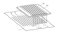
- FIG. 1 is a perspective view showing a laser processing apparatus according to a first embodiment of the present invention. It is a figure which shows the annealing aspect of a 1st area
- FIG. 10 is a diagram showing a step subsequent to that in FIG. 9.
- FIG. 11 is a diagram showing a step subsequent to FIG. 10. It is a graph which shows the effect of this invention.
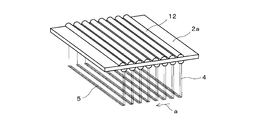
- two cylindrical lens arrays 2a and 2b are arranged in parallel above a substrate 1 to be laser-processed.
- each of the cylindrical lens arrays 2a and 2b for example, eight cylindrical lenses 12 are formed in parallel with each other at a predetermined lens pitch.
- Pulse laser light is controlled and output from a suitable pulse laser light source (not shown) by a suitable control device.
- the pulsed laser light emitted from the laser light source is shaped into a flat plate-like laser beam by the two cylindrical lens arrays 2a and 2b and irradiated onto the substrate.
- the irradiation region 5 of each beam 4 of the laser light has a band shape and is parallel to each other.
- the irradiation region 5 of the laser beam 4 has a width of 250 ⁇ m and a length of 50 mm.
- the pitch at the irradiation position of the laser beam 4 is the same as the pixel pitch, for example, 750 ⁇ m.
- the pitch of the laser beams 4 may be 2 or an integer multiple of the pixel pitch.
- the pitch of the laser beam 4 is made the same as the arrangement pitch (lens pitch) of the cylindrical lenses 12 of the cylindrical lens arrays 2a and 2b by adjusting the optical characteristics of the cylindrical lens arrays 2a and 2b and other optical systems. Can do.
- the cylindrical lens arrays 2a and 2b are prepared in advance so that the lens pitch of the cylindrical lenses corresponds to the pixel pitch of the liquid crystal display panel, and the panel to be processed from these cylindrical lens arrays 2a and 2b.
- the cylindrical lens arrays 2a and 2b By selecting the cylindrical lens arrays 2a and 2b to be used according to the pixel pitch, it is possible to easily configure the optical system.
- the substrate to be laser-processed has an a-Si film formed on a glass substrate.
- the a-Si film is irradiated with laser light, melted once, and then solidified to form a polycrystal. It can be modified into a silicon film.
- the glass substrate has a width of 1 m or 2 m, for example.
- pixel transistors and driving circuit transistors are formed by photolithography on all these panels, and then the panels are cut and separated. Thus, a plurality of display panels are manufactured at the same time.
- the laser light source is, for example, a Nd: YAG laser light having a wavelength of 1064 nm and a third harmonic of 355 nm and a frequency of, for example, 200 Hz.
- the pulsed laser light emitted from the laser light source is incident on the cylindrical lens arrays 2 a and 2 b shown in FIG. 1 and is shaped into a flat beam 4 by the cylindrical lens 12. Thereby, the surface of the substrate 1 is irradiated with the laser beam 4 having the irradiation region 5 in a band shape.
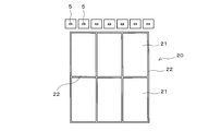
- FIG. 9 shows a 6-sheet glass substrate on which 6 liquid crystal display panels are formed on the glass substrate 20.
- Each display panel includes a pixel region 21 in which pixels as first regions are formed, and a peripheral region 22 in which drive circuits as second regions are formed.
- a gate electrode made of a metal film such as Al is patterned on a glass substrate by sputtering.
- a gate insulating film made of a SiN film is formed on the entire surface by low temperature plasma CVD at 250 to 300 ° C. using silane and H 2 gas as source gases.
- an a-Si: H film is formed on the gate insulating film by, eg, plasma CVD.
- This a-Si: H film is formed by using a mixed gas of silane and H 2 gas as a source gas.
- the region on the gate electrode of the a-Si: H film is a channel formation planned region, the channel formation scheduled region is annealed by irradiating with laser light, and the channel formation planned region is polycrystallized to form a polysilicon channel region. Form.
- FIG. 2 shows the laser irradiation mode of the pixel region
- FIGS. 3 to 8 show the laser irradiation mode of the peripheral region.
- the control device irradiates the laser beam when the substrate 1 is moved by the pixel pitch G.
- the control device irradiates the laser beam when the substrate 1 is moved by the pixel pitch G.
- the substrate 1 may be irradiated with a pulsed laser beam 4 each time it is detected.
- the substrate 1 is irradiated with eight laser beams 4 at intervals of the pixel pitch G in one shot. Each time the substrate 1 is relatively moved by the pixel pitch G, a pulse laser beam is shot.
- the laser shot is received 8 times at the position where the laser beam irradiation is performed on the substrate, and the a-Si film on the substrate is subjected to the laser treatment 8 times.
- a-Si is modified into polysilicon in the irradiated region 5 subjected to this laser treatment.
- the width of the irradiation region 5 of the pulse laser beam is 250 ⁇ m
- the length is 50 mm
- the pixel pitch G is 750 ⁇ m
- the size of one pixel transistor is 30 ⁇ m square.
- 5 is an area that sufficiently covers all the pixel transistors arranged in a line in a 50 mm long area.
- the amorphous silicon in all pixel transistor formation regions can be modified to polysilicon.
- the pixel pitch is 750 ⁇ m, the region of 500 ⁇ m is not irradiated with laser light. For this reason, the laser processing can be made efficient and quick, and the tact time can be shortened.
- the substrate 1 is relatively moved in the width direction by the width of the irradiation region 5, and then one shot of the laser beam 4 is irradiated. Thereby, the three-shot laser irradiation region 5 is formed continuously.
- the substrate 1 is relatively moved by the width of the irradiation region 5 in this width direction, and then one shot of the laser beam 4 is irradiated. As a result, four-shot laser irradiation regions 5 are formed continuously.
- the substrate 1 is relatively moved in the width direction by the width of the irradiation region 5, and then one shot of the laser beam 4 is irradiated. As a result, a 5-shot laser irradiation region 5 is formed continuously.
- the substrate 1 is relatively moved by the width of the irradiation region 5 in the width direction, and thereafter the operation of irradiating one shot of the laser beam 4 is repeated, whereby the peripheral circuit is
- the laser irradiation area 5 is connected in all areas 22, and the entire area 22 is subjected to laser processing.
- the first region for example, a pixel region
- the laser processing can be speeded up by thinning out the laser processing
- the region requiring the laser processing such as the pixel transistor formation scheduled region
- the second region for example, the peripheral region
- the formation region does not have periodicity and may be formed at an arbitrary position like the driving transistor
- the entire region is subjected to laser processing.
- the glass substrate 20 includes a pixel region 21 in which pixels are formed and a peripheral region 22 in which driver circuits and the like are formed in the formation regions of the display panels (six in the illustrated example).
- an optical system including the cylindrical lens array 2 a is positioned in accordance with the peripheral region 22, and the irradiation region 5 of the laser beam 4 is positioned on the peripheral region 22. That is, the cylindrical lens array 2 a is installed so that the longitudinal direction of the irradiation region 5 of the laser beam 4 straddles the width direction of the peripheral region 22.
- the substrate 1 is moved in the width direction of the irradiation region 5 relative to the cylindrical lens array 2a, and laser shot is performed by the steps shown in FIGS.
- the entire peripheral region 22 is laser-treated as shown in FIG.
- the laser processing region shown in FIG. 10 is a band-like region having a width of 50 mm (the length of the irradiation region 5), and a part of the pixel region 21 is also laser-processed beyond the peripheral region 22.
- the laser processing in the steps shown in FIGS. 3 to 8 is finally shifted in a direction (arrow c direction) orthogonal to the laser scanning direction as shown in FIG. That is, at the end of the step shown in FIG. 10, the cylindrical lens array 12a is shifted by the length of the irradiation region 5 in the direction (arrow c direction) perpendicular to the scanning direction shown by the arrow b in FIG.
- the laser shot is scanned in the reverse direction (arrow d direction) of FIG. 10.
- the irradiation region 5 is formed in the pixel region 21 according to the mode shown in FIG. 2. Go. Accordingly, in the pixel region 21, an irradiation region 5 having a pixel pitch G (750 ⁇ m) and a width of 250 ⁇ m is formed.
- the intermediate region of the irradiation region 5 is not laser processed.
- the region including the channel region of the pixel transistor in the pixel region 21 is laser-processed and modified into a polysilicon film.
- a plurality of display panels (eight in the illustrated example) can be obtained from one glass substrate 20, but when the laser scanning moves from the pixel region 21 to the pixel region 21 of another panel, the display panel Therefore, the entire peripheral region 23 is also laser-treated in the steps shown in FIGS. Thereafter, the same process is repeated, and the entire glass substrate is subjected to laser processing by a process of laser-shoting at a pixel pitch G and a process of laser-shoting so that the irradiation areas are continuous.
- the channel regions of the pixel transistor and the driving transistor are modified from amorphous silicon to polysilicon, and high speed operation of the transistor is ensured.
- the region where the transistor is not formed remains amorphous silicon.
- FIG. 12 is a graph showing the effect of the present invention with the panel size on the horizontal axis and the tact time on the vertical axis.
- ⁇ indicates the tact time when the entire surface of the substrate is laser processed using an excimer laser having a wavelength of 308 nm and a frequency of 600 Hz.
- ⁇ is the tact time when the entire surface of the substrate is laser processed using an Nd: YAG laser having a wavelength of 355 nm + 1064 nm and a frequency of 200 Hz.
- ⁇ is an embodiment of the present invention, and is a tact time when a substrate is laser-treated as shown in FIG.
- the present invention is effective in improving the tact time not only in the production of liquid crystal display panels but also in technical fields that require laser processing.
- the number of cylindrical lenses 12 formed in one cylindrical lens array 2a, 2b is eight in the above embodiment, but the present invention is not limited to this and can be variously set.
- the laser processing portion of the substrate 1 is usually subjected to the same number of laser processing according to the number of the cylindrical lenses 12, but one movement of the cylindrical lenses 2a and 2b is performed in the pixel.
- the pitch G twice or more the number of times of laser processing at the laser processing location on the substrate can be reduced to 1 ⁇ 2 or less of the number of cylindrical lenses 2a and 2b.
- the present invention is useful in a technical field that requires laser processing such as film modification, such as a display panel of a liquid crystal display device.
- Substrate 2a, 2b Cylindrical lens array 4: Laser beam 5: Irradiation region 12: Cylindrical lens 20: Glass substrate 21: Pixel region 22: Peripheral region 23: Peripheral region
Landscapes
- Physics & Mathematics (AREA)
- Optics & Photonics (AREA)
- Engineering & Computer Science (AREA)
- Plasma & Fusion (AREA)
- Mechanical Engineering (AREA)
- Recrystallisation Techniques (AREA)
Abstract
複数本のシリンドリカルレンズを有するシリンドリカルレンズアレイにより、例えば8個の平板状のレーザビームを整形し、これを基板上のa-Si膜に照射する。そして、基板をこのレーザビームの照射領域のギャップGで移動させて、細長い照射領域をギャップGで基板上に形成する。このギャップGを画素ピッチとすることにより、画素領域において、画素トランジスタの形成予定領域のみを照射領域とすることができる。これにより、a-Si膜をポリシリコン膜に改質するアニーリング処理等のレーザ処理を迅速化することができ、タクトタイムの短縮が可能である。
Description
本発明は、アモルファスシリコン膜(以下、a-Si膜という)にレーザ光を照射してアニールすることにより、a-Siを多結晶シリコン(以下、ポリシリコンという)に結晶化させる場合等に使用されるレーザ処理装置に関し、特に、複数個のシリンドリカルレンズを使用したレーザ処理装置に関する。
逆スタガ構造の薄膜トランジスタとしては、絶縁性基板上にCr又はAl等の金属層によりゲート電極を形成し、次いで、このゲート電極を含む基板上にゲート絶縁膜として例えばSiN膜を形成し、その後、全面に水素化アモルファスシリコン(以下、a-Si:Hと記載する)膜を形成し、このa-Si:H膜をゲート電極上の所定領域にアイランド状にパターニングし、更に、金属層によりソース・ドレイン電極を形成したアモルファスシリコントランジスタがある。
しかしながら、このアモルファスシリコントランジスタは、a-Si:H膜をチャネル領域に使用しているので、チャネル領域における電荷の移動度が小さいという難点がある。このため、アモルファスシリコントランジスタは、例えば、液晶表示装置の画素部の画素トランジスタとしては使用可能であるが、高速の書き換えが要求される周辺駆動回路の駆動トランジスタとしては、チャネル領域の電荷移動度が小さすぎて、使用することが困難である。
一方、多結晶シリコン膜を直接基板上に形成しようとすると、LPCVD(減圧化学気相成長)法により形成することになるが、これは1500℃程度の高温プロセスになるため、液晶表示装置のようなガラス基板(軟化点が400~500℃)上に多結晶シリコン膜を直接形成することはできない。
そこで、一旦、チャネル領域にa-Si:H膜を形成し、その後、このa-Si:H膜にYAGエキシマレーザ等のレーザ光を照射してレーザアニールすることにより、極短時間での溶融凝固の相転移により、a-Si:H膜をポリシリコン膜に結晶化させる低温ポリシリコンプロセスが採用されるようになっている。これにより、ガラス基板上のチャネル領域を電荷移動度が高くトランジスタ動作の高速化が可能なポリシリコン膜により形成することが可能になる(特許文献1)。
また、この種のレーザアニール装置において、パルスレーザ光を1個のシリンドリカルレンズにより、基板上の照射領域が帯状のビームになるように整形して、このレーザ光学系又は基板を相対的に前記照射領域の幅方向に移動させることにより、レーザ光で基板上の全領域を走査することにより、a-Si:H膜をポリシリコン膜に結晶化させるものがある。
しかしながら、上述の従来のレーザ処理技術は、基板上の照射領域におけるビーム長が例えば750mm、ビーム幅が例えば350μmと狭く、細長い帯状のレーザ光をその幅方向に走査して、レーザ光を基板の全域で走査させてレーザ処理しているために、処理時間が長く、タクトタイムが長いという問題点がある。
本発明はかかる問題点に鑑みてなされたものであって、a-Si膜をポリシリコン膜に改質するアニーリング処理等のレーザ処理を迅速化することができ、タクトタイムの短縮が可能な処理装置を提供することを目的とする。
本発明に係るレーザ処理装置は、パルスレーザ光を発光するレーザ光源と、このレーザ光源からのパルスレーザ光を基板上の照射領域が複数本の帯状になるように整形する複数個のシリンドリカルレンズと、前記基板と前記シリンドリカルレンズとを前記照射領域の幅方向及び長手方向に相対的に移動させるように制御する制御装置と、を有し、前記シリンドリカルレンズはその長手方向に垂直の方向に一定のレンズピッチで相互に平行に配置されており、前記制御装置は、前記基板上の第1領域では、前記帯状の照射領域がその幅方向に第1ピッチとなるようにパルスレーザ光を照射し、第2領域では、前記帯状の照射領域がその幅方向に前記第1ピッチよりも小さい第2ピッチでパルスレーザ光を照射するように前記レーザ光源の発光と前記基板及び前記シリンドリカルレンズの相対的移動を制御することを特徴とする。
このレーザ処理装置は、a-Si膜をポリシリコン膜に改質するアニーリング処理に特に有効である。また、1個のガラス基板から、液晶表示装置の複数個のパネルを製造する際に適用すると、特に有効である。
そこで、本発明の一態様として、前記基板は、1又は複数個の液晶表示パネルを製造するガラス基板であり、前記第1領域は画素領域であり、前記第2領域は駆動回路を形成する前記パネルの周辺領域である場合、前記制御装置は、例えば、前記ガラス基板上の前記第1領域では、前記パルスレーザ光の照射領域が画素領域の画素ピッチと一致するように前記パルスレーザ光を照射し、前記ガラス基板上の前記第2領域では、前記パルスレーザ光の照射領域がその幅方向に相互に連なるようにその幅以下のピッチでパルスレーザ光を照射するように制御する。また、前記基板にはアライメントマークが画素ピッチGで複数個形成されており、このアライメントマークを撮像するカメラを設け、前記制御装置は、前記カメラが、基板上のアライメントマークを検出する都度、パルスレーザ光を照射させるように制御することもできる。
本発明においては、例えば、液晶表示装置のパネルの製造に使用した場合、画素は、所定の画素ピッチで配置されているので、前記照射領域の第1ピッチを画素ピッチと同一としておくことにより、制御装置は、画素領域(第1領域)においては、帯状のパルスレーザ光を、画素ピッチと同一のピッチで照射することができる。これにより、画素領域における画素が形成されるべき箇所については、レーザ処理によりポリシリコンへの改質処理を行うことができ、その間の領域は、レーザ処理しないので、全体の処理を高効率化して、タクトタイムを短縮できる。一方、パネルの周辺部に配置されるドライブ回路の形成領域(第2領域)においては、パルスレーザ光を画素ピッチよりも小さいピッチで、パルスレーザ光を照射することにより、レーザ処理領域を第1領域よりも広くして、駆動回路の形成位置の任意性を高め、駆動回路の形成位置の選択範囲を広くすることができる。このとき、第2領域においては、第2ピッチをパルスレーザ光の幅と同一とすることにより、パルスレーザ光の照射領域を、その幅方向に連ねることができ、第2領域においては、その全域でレーザ処理(ポリシリコン化)することができる。
従って、本発明によれば、第1領域では、レーザ処理が不要な部分はレーザ光を照射しないようにして照射領域を間引いてレーザ処理するので、基板の全域でレーザ処理することはなく、高速でレーザ処理することができ、処理のタクトタイムを短縮することができる。
以下、本発明の実施形態について、添付の図面を参照して具体的に説明する。図1に示すように、レーザ処理すべき基板1の上方に、シリンドリカルレンズアレイ2a、2bが2枚平行に設置されている。各シリンドリカルレンズアレイ2a、2bには、例えば、8本のシリンドリカルレンズ12が相互に平行に所定のレンズピッチで形成されている。適宜のパルスレーザ光源(図示せず)からパルスレーザ光が、適宜の制御装置により制御されて出力される。このレーザ光源から出射されたパルスレーザ光は、2枚のシリンドリカルレンズアレイ2a、2bにより、平板状のレーザビームに整形されて基板上に照射される。よって、基板上において、レーザ光の各ビーム4の照射領域5は帯状をなし、相互に平行である。このレーザビーム4の照射領域5は、例えば、幅が250μmであり、長さが50mmである。また、レーザビーム4の照射位置におけるピッチは、画素ピッチと同一であり、例えば、750μmである。又は、このレーザビーム4のピッチは、画素ピッチの2又は整数倍でもよい。このレーザビーム4のピッチは、シリンドリカルレンズアレイ2a、2b及びその他の光学系の光学特性を調整することにより、シリンドリカルレンズアレイ2a、2bのシリンドリカルレンズ12の配列ピッチ(レンズピッチ)と同一とすることができる。よって、このシリンドリカルレンズのレンズピッチを、液晶表示パネルの画素ピッチに対応させて、予めシリンドリカルレンズアレイ2a、2bを用意しておき、これらのシリンドリカルレンズアレイ2a、2bの中から、処理すべきパネルの画素ピッチに応じて使用するシリンドリカルレンズアレイ2a、2bを選択することにより、容易に光学系を構成することができる。
レーザ処理すべき基板は、ガラス基板の上に、a-Si膜が形成されており、このa-Si膜にレーザ光を照射して、これを一旦溶融させた後、凝固させることにより、ポリシリコン膜に改質することができる。このガラス基板の大きさは、例えば、幅が1m又は2mである。そして、通常、1枚のガラス基板1上上に複数枚のパネルを形成し、その後、これらの全てのパネルについて、フォトリソグラフィにより画素トランジスタ及び駆動回路トランジスタ等を形成し、その後,パネルを切断分離して、複数枚の表示パネルを同時に製造する。
次に、本実施形態の動作について、制御装置の制御態様と共に説明する。レーザ光源は、例えば、波長が1064nmのレーザ光とその3次高調波の355nmを含み、その周波数は例えば200HzであるNd:YAGレーザ光である。このレーザ光源から出射されたパルスレーザ光は、図1に示すシリンドリカルレンズアレイ2a、2bに入射し、シリンドリカルレンズ12により、平板状のビーム4に整形される。これにより、基板1の表面には、照射領域5が帯状のレーザビーム4が照射される。
図9は、ガラス基板20上に6枚の液晶表示パネルが形成される6枚取りのガラス基板を示す。この各表示パネルは、第1領域としての画素が形成される画素領域21と、第2領域としての駆動回路が形成される周辺領域22とから構成される。
例えば、液晶表示装置の周辺回路として、画素の駆動トランジスタを形成する場合、ガラス基板上にAl等の金属膜からなるゲート電極を、スパッタによりパターン形成する。そして、シラン及びH2ガスを原料ガスとし、250~300℃の低温プラズマCVD法により、全面にSiN膜からなるゲート絶縁膜を形成する。その後、ゲート絶縁膜上に、例えば、プラズマCVD法によりa-Si:H膜を形成する。このa-Si:H膜はシランとH2ガスを混合したガスを原料ガスとして成膜する。このa-Si:H膜のゲート電極上の領域をチャネル形成予定領域として、このチャネル形成予定領域にレーザ光を照射してアニールし、このチャネル形成予定領域を多結晶化してポリシリコンチャネル領域を形成する。
このレーザ処理に際し、図2は、画素領域のレーザ照射態様を示し、図3乃至図8は、周辺領域のレーザ照射態様を示す。先ず、図2に示す画素領域においては、シリンドリカルレンズアレイ2a、2bの例えば8個のシリンドリカルレンズ12により、画素ピッチGと同一ピッチで、例えば、8個のレーザビーム4が基板1上に照射される。そして、制御装置が、基板1又はレーザ照射系を相対的にレーザビーム4の照射領域5の幅方向(矢印a方向)に移動させる。このとき、例えば、基板1をa方向に移動させる場合、制御装置は、基板1が画素ピッチGだけ移動したときに、レーザ光を照射する。これは、例えば、基板1にアライメントマークを画素ピッチGで複数個形成しておき、このアライメントマークをカメラ(図示せず)により撮像し、基板1がa方向に移動してカメラによりアライメントマークが検出される都度、パルス状のレーザビーム4を基板1に照射すればよい。これにより、基板1には1ショットで8個のレーザビーム4が画素ピッチGの間隔で照射される。そして、画素ピッチGだけ基板1を相対的に移動させる都度、パルスレーザ光のショットを行う。これにより、定常状態では、基板上において1カ所のレーザビーム照射を受けた位置では、8回、レーザショットを受けることになり、基板上のa-Si膜は、8回、レーザ処理を受ける。これにより、このレーザ処理を受けた照射領域5において、a-Siがポリシリコンに改質される。前述のごとく、例えば、パルスレーザ光の照射領域5の幅は250μm、長さは50mmであり、画素ピッチGは750μmであり、1個の画素トランジスタの大きさが30μm四方であるから、照射領域5は50mmの長さの領域に1列に並ぶ全ての画素トランジスタを十分にカバーする領域であり、この画素ピッチG毎に照射領域5を形成して、基板をレーザ光で走査することにより、全ての画素トランジスタ形成予定領域のアモルファスシリコンをポリシリコンに改質することができる。一方、画素ピッチが750μmであるから、500μmの領域には、レーザ光が照射されない。このため、レーザ処理を効率化及び迅速化することができ、タクトタイムを短縮することができる。
一方、周辺領域22の駆動回路の形成領域においては、図3に示すように、1ショットのレーザビーム4の照射を行い、1個の照射領域5を形成した後、図4に示すように、基板1を相対的に照射領域5の幅だけ、この幅方向(a方向)に移動させ(シフトさせ)、その後、1ショットのレーザビーム4を照射する。これにより、2ショットのレーザ照射領域5が連なって形成される。
次に、図5に示すように、基板1を相対的に照射領域5の幅だけ、この幅方向に移動させ、その後、1ショットのレーザビーム4を照射する。これにより、3ショットのレーザ照射領域5が連なって形成される。
次に、図6に示すように、基板1を相対的に照射領域5の幅だけ、この幅方向に移動させ、その後、1ショットのレーザビーム4を照射する。これにより、4ショットのレーザ照射領域5が連なって形成される。
次に、図7に示すように、基板1を相対的に照射領域5の幅だけ、この幅方向に移動させ、その後、1ショットのレーザビーム4を照射する。これにより、5ショットのレーザ照射領域5が連なって形成される。
次に、図8に示すように、基板1を相対的に照射領域5の幅だけ、この幅方向に移動させ、その後、1ショットのレーザビーム4を照射するという動作を繰り返すことにより、周辺回路22の全領域にてレーザ照射領域5が連なり、周辺領域22の全領域がレーザ処理を受ける。
このようにして、レーザ処理を間引いてレーザ処理を迅速化することができる第1領域(例えば、画素領域)では、画素トランジスタ形成予定領域のようにレーザ処理が必要な領域のみ、レーザ処理し、駆動トランジスタのように、形成予定領域に周期性が無く、任意の位置に形成する場合があるような第2領域(例えば,周辺領域)では、その全ての領域にレーザ処理する。これにより、従来よりも、レーザ処理を迅速化することができ、タクトタイムを短縮することができる。
次に、第1領域及び第2領域のレーザ照射態様について説明する。図9に示すように、ガラス基板20には、その各表示パネルの形成領域(図示例は、6個)に、画素が形成される画素領域21とドライバ回路等が形成される周辺領域22とが設けられているが、先ず、この周辺領域22に合わせて、シリンドリカルレンズアレイ2aを含む光学系を位置させ、レーザビーム4の照射領域5をこの周辺領域22上に位置させる。つまり、このレーザビーム4の照射領域5の長手方向がこの周辺領域22の幅方向をまたぐようにシリンドリカルレンズアレイ2aを設置する。そして、図10に矢印bにて示すように、基板1をシリンドリカルレンズアレイ2aに対して相対的に照射領域5の幅方向に移動させ、図3乃至図8に示す工程によりレーザショットを行い、照射領域5を連ねることにより、周辺領域22の全域を図8に示すようにレーザ処理する。このとき、図10に示すレーザ処理領域は、幅が50mm(照射領域5の長さ)の帯状の領域となり、周辺領域22を超えて画素領域21の一部もレーザ処理される。この図3乃至図8に示す工程のレーザ処理は、最終的に、図10に示すように、レーザ走査方向に直交する方向(矢印c方向)にシフトされて、終了する。つまり、図10に示す工程の最後において、シリンドリカルレンズアレイ12aは、図10に矢印bにて示す走査方向に垂直の方向(矢印c方向)に、照射領域5の長さ分シフトする。
その後、図11に示すように、レーザショットを図10の逆方向(矢印d方向)に走査するが、このとき、画素領域21においては、図2に示す態様により、照射領域5を形成していく。従って、画素領域21において、画素ピッチG(750μm)で幅が250μmの照射領域5が形成される。この照射領域5の中間の領域は、レーザ処理されない。これにより、画素領域21内の画素トランジスタのチャネル領域を含む領域が、レーザ処理されて、ポリシリコン膜に改質される。なお、1枚のガラス基板20から複数枚(図示例は8枚)の表示パネルが得られるが、レーザ走査が、画素領域21から別のパネルの画素領域21に移動する際には、パネル間の周辺領域23を通過するので、この周辺領域23も、図3乃至図8に示す工程でその全域をレーザ処理する。以後、同様の工程を繰り返して、ガラス基板の全域を、画素ピッチGでレーザショットする工程と、照射領域が連なるようにレーザショットする工程とにより、レーザ処理する。
このようにして、画素トランジスタ及び駆動トランジスタのチャネル領域は、アモルファスシリコンからポリシリコンに改質され、トランジスタ動作の高速化が確保される。一方、トランジスタが形成されない領域は、アモルファスシリコンのままである。これにより、レーザ処理の迅速化及び高速化を図ることができ、レーザ処理のタクトタイムを短縮することができる。
図12は、横軸にパネルサイズをとり、縦軸にタクトタイムをとって、本発明の効果を示すグラフ図である。図中、■は、波長が308nmで周波数が600Hzのエキシマレーザを使用して基板の全面をレーザ処理した場合のタクトタイムである。また、▲は波長が355nm+1064nmで周波数が200HzのNd:YAGレーザを使用して基板の全面をレーザ処理した場合のタクトタイムである。これに対し、◆は、本発明の実施形態であり、波長が355nm+1064nmで周波数が200HzのNd:YAGレーザを使用して、基板を図11に示すようにレーザ処理した場合のタクトタイムである。この図12から明らかなように、パネルサイズが20インチの場合はあまり効果がないが、パネルサイズが40インチから70インチになるにつれて、タクトタイムが大幅に短くなっている。パネルサイズが大きいほど、本発明の効果が大きいのは、パネルサイズが大きくなると、画素領域の面積が周辺領域の面積に比して、相対的に大きくなるからである。
本発明は、液晶表示パネルの製造に限らず、レーザ処理が必要な技術分野において、そのタクトタイムの向上に有効である。また、1個のシリンドリカルレンズアレイ2a、2bに形成するシリンドリカルレンズ12の数は、上記実施形態では8個であったが、本発明は、これに限らず、種々設定することができる。図2に示す工程においては、基板1のレーザ処理箇所は、通常、このシリンドリカルレンズ12の個数に応じて、それと同数のレーザ処理を受けるが、シリンドリカルレンズ2a、2bの1回の移動を、画素ピッチGの2倍以上とすることにより、基板上のレーザ処理箇所のレーザ処理の回数を、シリンドリカルレンズ2a、2bの数の1/2以下に減じることもできる。
本発明は、液晶表示装置の表示パネルのように、膜の改質のようにレーザ処理が必要な技術分野に有益である。
1:基板
2a、2b:シリンドリカルレンズアレイ
4:レーザビーム
5:照射領域
12:シリンドリカルレンズ
20:ガラス基板
21:画素領域
22:周辺領域
23:周辺領域
2a、2b:シリンドリカルレンズアレイ
4:レーザビーム
5:照射領域
12:シリンドリカルレンズ
20:ガラス基板
21:画素領域
22:周辺領域
23:周辺領域
Claims (3)
- パルスレーザ光を発光するレーザ光源と、このレーザ光源からのパルスレーザ光を基板上の照射領域が複数本の帯状になるように整形する複数個のシリンドリカルレンズと、前記基板と前記シリンドリカルレンズとを前記照射領域の幅方向及び長手方向に相対的に移動させるように制御する制御装置と、を有し、前記シリンドリカルレンズはその長手方向に垂直の方向に一定のレンズピッチで相互に平行に配置されており、前記制御装置は、前記基板上の第1領域では、前記帯状の照射領域がその幅方向に第1ピッチとなるようにパルスレーザ光を照射し、第2領域では、前記帯状の照射領域がその幅方向に前記第1ピッチよりも小さい第2ピッチでパルスレーザ光を照射するように前記レーザ光源の発光と前記基板及び前記シリンドリカルレンズの相対的移動を制御することを特徴とするレーザ処理装置。
- 前記基板は、1又は複数個の液晶表示パネルを製造するガラス基板であり、前記第1領域は画素領域であり、前記第2領域は駆動回路を形成する前記パネルの周辺領域であり、前記制御装置は、前記ガラス基板上の前記第1領域では、前記パルスレーザ光の照射領域が画素領域の画素ピッチと一致するように前記パルスレーザ光を照射し、前記ガラス基板上の前記第2領域では、前記パルスレーザ光の照射領域がその幅方向に相互に連なるようにその幅以下のピッチでパルスレーザ光を照射するように制御することを特徴とする請求項1に記載のレーザ処理装置。
- 前記基板にはアライメントマークが画素ピッチGで複数個形成されており、このアライメントマークを撮像するカメラを設け、前記制御装置は、前記カメラが、基板上のアライメントマークを検出する都度、パルスレーザ光を照射させることを特徴とする請求項1又は2に記載のレーザ処理装置。
Applications Claiming Priority (2)
| Application Number | Priority Date | Filing Date | Title |
|---|---|---|---|
| JP2011109797A JP5800292B2 (ja) | 2011-05-16 | 2011-05-16 | レーザ処理装置 |
| JP2011-109797 | 2011-05-16 |
Publications (1)
| Publication Number | Publication Date |
|---|---|
| WO2012157410A1 true WO2012157410A1 (ja) | 2012-11-22 |
Family
ID=47176746
Family Applications (1)
| Application Number | Title | Priority Date | Filing Date |
|---|---|---|---|
| PCT/JP2012/060941 Ceased WO2012157410A1 (ja) | 2011-05-16 | 2012-04-24 | レーザ処理装置 |
Country Status (3)
| Country | Link |
|---|---|
| JP (1) | JP5800292B2 (ja) |
| TW (1) | TWI521563B (ja) |
| WO (1) | WO2012157410A1 (ja) |
Cited By (1)
| Publication number | Priority date | Publication date | Assignee | Title |
|---|---|---|---|---|
| WO2020090396A1 (ja) * | 2018-11-02 | 2020-05-07 | 株式会社ブイ・テクノロジー | レーザアニール装置およびレーザアニール方法 |
Families Citing this family (5)
| Publication number | Priority date | Publication date | Assignee | Title |
|---|---|---|---|---|
| JP6756737B2 (ja) | 2015-12-25 | 2020-09-16 | ギガフォトン株式会社 | レーザ照射装置 |
| JPWO2017163356A1 (ja) | 2016-03-24 | 2019-01-31 | 国立大学法人九州大学 | レーザドーピング装置及び半導体装置の製造方法 |
| US10811286B2 (en) | 2016-09-28 | 2020-10-20 | Sakai Display Products Corporation | Laser annealing device and laser annealing method |
| JP2019121743A (ja) * | 2018-01-10 | 2019-07-22 | 株式会社ブイ・テクノロジー | レーザ照射装置、及び、レーザ照射方法 |
| CN114654108B (zh) * | 2022-04-09 | 2023-06-23 | 法特迪精密科技(苏州)有限公司 | Mems探针硅片切割装置 |
Citations (3)
| Publication number | Priority date | Publication date | Assignee | Title |
|---|---|---|---|---|
| JPH07307304A (ja) * | 1994-05-13 | 1995-11-21 | Semiconductor Energy Lab Co Ltd | 半導体デバイスのレーザー処理方法 |
| JPH09199729A (ja) * | 1996-01-12 | 1997-07-31 | Seiko Epson Corp | 半導体膜の結晶化方法、アクティブマトリクス基板及び液晶表示装置 |
| JP2004253599A (ja) * | 2003-02-20 | 2004-09-09 | Hitachi Ltd | パネル型表示装置とその製造方法および製造装置 |
-
2011
- 2011-05-16 JP JP2011109797A patent/JP5800292B2/ja not_active Expired - Fee Related
-
2012
- 2012-04-24 WO PCT/JP2012/060941 patent/WO2012157410A1/ja not_active Ceased
- 2012-05-10 TW TW101116692A patent/TWI521563B/zh not_active IP Right Cessation
Patent Citations (3)
| Publication number | Priority date | Publication date | Assignee | Title |
|---|---|---|---|---|
| JPH07307304A (ja) * | 1994-05-13 | 1995-11-21 | Semiconductor Energy Lab Co Ltd | 半導体デバイスのレーザー処理方法 |
| JPH09199729A (ja) * | 1996-01-12 | 1997-07-31 | Seiko Epson Corp | 半導体膜の結晶化方法、アクティブマトリクス基板及び液晶表示装置 |
| JP2004253599A (ja) * | 2003-02-20 | 2004-09-09 | Hitachi Ltd | パネル型表示装置とその製造方法および製造装置 |
Cited By (1)
| Publication number | Priority date | Publication date | Assignee | Title |
|---|---|---|---|---|
| WO2020090396A1 (ja) * | 2018-11-02 | 2020-05-07 | 株式会社ブイ・テクノロジー | レーザアニール装置およびレーザアニール方法 |
Also Published As
| Publication number | Publication date |
|---|---|
| TWI521563B (zh) | 2016-02-11 |
| JP5800292B2 (ja) | 2015-10-28 |
| TW201248691A (en) | 2012-12-01 |
| JP2012243818A (ja) | 2012-12-10 |
Similar Documents
| Publication | Publication Date | Title |
|---|---|---|
| JP5495043B2 (ja) | レーザアニール方法、装置及びマイクロレンズアレイ | |
| US20080087895A1 (en) | Polysilicon thin film transistor and method of fabricating the same | |
| KR20020091352A (ko) | 실리콘막의 결정화 방법 | |
| JP5800292B2 (ja) | レーザ処理装置 | |
| WO2011158612A1 (ja) | 低温ポリシリコン膜の形成装置及び方法 | |
| WO2018016146A1 (ja) | レーザ照射装置、薄膜トランジスタおよび薄膜トランジスタの製造方法 | |
| KR20140018081A (ko) | 박막 반도체 장치의 제조 방법, 박막 반도체 어레이 기판의 제조 방법, 결정성 실리콘 박막의 형성 방법, 및 결정성 실리콘 박막의 형성 장치 | |
| CN112447506B (zh) | 激光退火装置 | |
| US20100051830A1 (en) | Semiconductor processing apparatus and semiconductor processing method | |
| JP2006013050A (ja) | レーザビーム投影マスク及びそれを用いたレーザ加工方法、レーザ加工装置 | |
| CN110998795A (zh) | 激光照射装置、薄膜晶体管的制造方法及投影掩模 | |
| JP6761479B2 (ja) | レーザ照射装置、薄膜トランジスタおよび薄膜トランジスタの製造方法 | |
| JP7154592B2 (ja) | レーザアニール方法およびレーザアニール装置 | |
| US10840095B2 (en) | Laser irradiation device, thin-film transistor and thin-film transistor manufacturing method | |
| KR101186294B1 (ko) | 측면 결정화된 반도체층의 제조방법 및 이를 이용한 박막트랜지스터의 제조방법 | |
| KR102034136B1 (ko) | 박막 트랜지스터 기판의 제조방법 | |
| WO2006075568A1 (ja) | 多結晶半導体薄膜の製造方法および製造装置 | |
| JP4769491B2 (ja) | 結晶化方法、薄膜トランジスタの製造方法、薄膜トランジスタおよび表示装置 | |
| WO2020184153A1 (ja) | レーザアニール装置 | |
| WO2019138674A1 (ja) | レーザ照射装置、及び、レーザ照射方法 | |
| KR20050121548A (ko) | 실리콘 결정화 방법과 이를 이용한 박막트랜지스터 기판의제조방법 | |
| KR20050121549A (ko) | 실리콘 결정화 방법과 이를 위한 레이저 장치 그리고 이를이용한 박막트랜지스터 기판의 제조방법 | |
| CN111033693A (zh) | 激光照射装置、薄膜晶体管的制造方法、程序及投影掩模 | |
| WO2018092213A1 (ja) | レーザ照射装置および薄膜トランジスタの製造方法 | |
| JP2008147236A (ja) | 結晶化装置およびレーザ加工方法 |
Legal Events
| Date | Code | Title | Description |
|---|---|---|---|
| 121 | Ep: the epo has been informed by wipo that ep was designated in this application |
Ref document number: 12786357 Country of ref document: EP Kind code of ref document: A1 |
|
| NENP | Non-entry into the national phase |
Ref country code: DE |
|
| 122 | Ep: pct application non-entry in european phase |
Ref document number: 12786357 Country of ref document: EP Kind code of ref document: A1 |