WO2012157077A1 - 水晶発振器付き恒温槽の温度制御装置、無線送信装置、無線受信装置、無線送受信装置及び無線基地局 - Google Patents
水晶発振器付き恒温槽の温度制御装置、無線送信装置、無線受信装置、無線送受信装置及び無線基地局 Download PDFInfo
- Publication number
- WO2012157077A1 WO2012157077A1 PCT/JP2011/061323 JP2011061323W WO2012157077A1 WO 2012157077 A1 WO2012157077 A1 WO 2012157077A1 JP 2011061323 W JP2011061323 W JP 2011061323W WO 2012157077 A1 WO2012157077 A1 WO 2012157077A1
- Authority
- WO
- WIPO (PCT)
- Prior art keywords
- crystal oscillator
- temperature control
- temperature
- thermostatic chamber
- unit
- Prior art date
- Legal status (The legal status is an assumption and is not a legal conclusion. Google has not performed a legal analysis and makes no representation as to the accuracy of the status listed.)
- Ceased
Links
Images




Classifications
-
- H—ELECTRICITY
- H03—ELECTRONIC CIRCUITRY
- H03L—AUTOMATIC CONTROL, STARTING, SYNCHRONISATION OR STABILISATION OF GENERATORS OF ELECTRONIC OSCILLATIONS OR PULSES
- H03L1/00—Stabilisation of generator output against variations of physical values, e.g. power supply
- H03L1/02—Stabilisation of generator output against variations of physical values, e.g. power supply against variations of temperature only
- H03L1/022—Stabilisation of generator output against variations of physical values, e.g. power supply against variations of temperature only by indirect stabilisation, i.e. by generating an electrical correction signal which is a function of the temperature
-
- H—ELECTRICITY
- H03—ELECTRONIC CIRCUITRY
- H03L—AUTOMATIC CONTROL, STARTING, SYNCHRONISATION OR STABILISATION OF GENERATORS OF ELECTRONIC OSCILLATIONS OR PULSES
- H03L1/00—Stabilisation of generator output against variations of physical values, e.g. power supply
- H03L1/02—Stabilisation of generator output against variations of physical values, e.g. power supply against variations of temperature only
- H03L1/028—Stabilisation of generator output against variations of physical values, e.g. power supply against variations of temperature only of generators comprising piezoelectric resonators
Definitions
- This case relates to a temperature control device for a thermostatic chamber with a crystal oscillator, a wireless transmission device, a wireless reception device, a wireless transmission / reception device, and a wireless base station.
- a crystal oscillator with a thermostatic bath (OCXO: Oven Controlled Crystal Oscillator) is known as a crystal oscillator that is not easily influenced by the environmental temperature and has a stable frequency characteristic.
- This crystal oscillator with a thermostat is a crystal oscillator as a crystal oscillator mounted in a thermostat which is a case where the temperature is kept constant.
- FIG. 1 is a diagram illustrating an example of a configuration of a conventional apparatus.
- a conventional apparatus illustrated in FIG. 1 includes a quartz oscillator 3, an electric heater (hereinafter simply referred to as “heater”) 4, a temperature detection element 5, and a temperature control unit 5.
- a power transistor 6, a resistor 7 and a capacitor 8 are provided. That is, the conventional device illustrated in FIG. 1 changes the collector voltage of the power transistor 6 based on the internal temperature of the thermostat 2 detected by the temperature detection element 5 in order to keep the temperature inside the thermostat 2 constant. As a result, the voltage applied to both ends of the heater 4 is adjusted.
- the resistor 7 and the capacitor 8 function to moderate a change in the current flowing through the heater 4 in order to avoid sharp switching by the heater 4. According to the configuration shown in FIG. 1, power loss occurs in the power transistor 6 and heat is generated. Therefore, the power transistor 6 is disposed inside the thermostat 2 and used in order to effectively use the heat generated in the power transistor 6. (See Patent Document 1 below).
- the capacity of the capacitor 8 must be increased in order to moderate the change in the current flowing through the heater 4 having a small resistance value by the capacitor 8 connected in parallel with the heater 4. I must. For this reason, the size of the capacitor 8 itself is increased, and it is difficult to reduce the size of the apparatus. Further, in the conventional apparatus illustrated in FIG. 1, since the inside of the thermostatic chamber 2 is kept at a high temperature, if the power transistor 6 is arranged inside the thermostatic chamber 2, the power transistor 6 is subjected to temperature stress, and the reliability is increased. Deteriorates.
- the present invention is not limited to the above-described object, and other effects of the present invention can be achieved by the functions and effects derived from the respective configurations shown in the embodiments for carrying out the invention which will be described later. It can be positioned as one of
- a thermostatic chamber having a crystal oscillator that outputs an oscillation signal therein, a heater that heats the inside of the thermostatic chamber, a temperature detection unit that detects the temperature inside the thermostatic chamber, A switching element that performs on / off control of the heater, and a temperature control unit that receives a detection result from the temperature detection unit and an oscillation signal from the crystal oscillator, and controls the switching element on / off in synchronization with the oscillation signal. It is possible to use a temperature control device for a thermostatic chamber with a crystal oscillator that is provided.
- a wireless transmission device provided with a transmission unit that operates with an oscillation signal from the crystal oscillator in the temperature control device of the thermostatic chamber with the crystal oscillator described above can be used.
- a wireless receiver provided with a receiver that operates in response to an oscillation signal from the crystal oscillator in the temperature control device of the thermostatic chamber with the crystal oscillator described above can be used.
- a wireless transmission / reception apparatus including the wireless transmission apparatus and the wireless reception apparatus can be used.
- a radio base station having the above-described temperature control device for a thermostatic chamber with a crystal oscillator can be used.
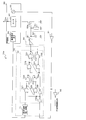
- FIG. 2 is a temperature control device for a thermostatic chamber with a crystal oscillator according to one embodiment (hereinafter referred to as “this device” as appropriate). It is a figure which shows an example of a structure.
- the temperature control device 10 for a thermostatic chamber with a crystal oscillator illustratively includes a thermostat 20, a crystal oscillator 30 disposed in the thermostat 20, an electric heater (hereinafter simply referred to as “heater”) 40, and temperature detection.
- the device 50 includes a switching device 60, a temperature control unit 70, a delay unit 80, and NOT circuits 91 and 92 arranged outside the thermostatic chamber 20.
- the thermostat 20 is a case for keeping the internal temperature constant, and is configured by applying a heat insulation layer with a metal casing, a heat insulation material, or the like. That is, the thermostatic chamber 20 functions as an example of a thermostatic chamber having a crystal oscillator 30 that outputs an oscillation signal.
- the crystal oscillator 30 is connected to the power supply terminal (Vcc) and outputs an oscillation signal having a frequency depending on the ambient temperature.
- the oscillation signal output from the crystal oscillator 30 is output to the temperature control unit 70 through the NOT circuit 91 and output to the outside through the NOT circuits 91 and 92.
- the heater 40 is connected to a power supply terminal (Vcc), generates heat when the temperature inside the thermostat 40 decreases, and heats the inside of the thermostat 20.
- the heater 40 is turned on and off by a switching element 60 described later. That is, the heater 40 functions as an example of a heater that heats the inside of the constant temperature bath 20.
- the temperature detecting element 50 detects the temperature inside the thermostatic chamber 20 and outputs a signal having a level corresponding to the detected temperature, and an element having temperature-dependent characteristics such as a thermistor can be used. That is, the temperature detection element 50 functions as an example of a temperature detection unit that detects the temperature inside the constant temperature bath 20.
- the switching element 60 controls on / off of the heater 40 by switching, and a power transistor is used in this example.
- the collector of the power transistor is connected to the heater 40, the emitter is grounded, and a control signal output from a delay unit 80 described later is input to the base. That is, the switching element 60 functions as an example of a switching element that performs on / off control of the heater 40. In general, it is known that noise at the output of the crystal oscillator 30 is generated at the rise and fall of the oscillation output.
- the temperature control unit 70 controls the on / off timing of the heater 40 to synchronize the two noise generation timings and suppress the noise generation when the heater 40 is on / off.
- the temperature control unit 70 outputs a control signal for controlling on / off of the heater 40 based on the outputs of the crystal oscillator 30 and the temperature detection element 50.
- the temperature control unit 70 includes a set temperature detection circuit 71 and a synchronization circuit 72.
- the set temperature detection circuit 71 outputs a signal for turning on the heater 40 based on the output of the temperature detection element 50.
- the set temperature detection circuit 71 determines whether or not the temperature corresponding to the output of the temperature detection element 50 has fallen below a value serving as a reference for switching on / off the heater 40 (hereinafter also referred to as a heater on / off reference value). When it is determined that the temperature corresponding to the output of the temperature detection element 50 has decreased below the heater on / off reference value, a signal for turning on the heater 40 is output, and the temperature corresponding to the output of the temperature detection element 50 is the heater on / off reference value. If it is determined that the value is greater than or equal to the value, a signal for turning on the heater 40 is not output.
- the set temperature detection circuit 71 receives a detection result from the temperature detection element 50 which is an example of a temperature detection unit, and outputs an on / off signal as a comparison result between the temperature inside the thermostat 20 and the heater on / off reference value. It functions as an example of a unit.
- the temperature detection element 50 may be an element that switches output on and off according to the detected temperature, such as a thermal relay using a bimetal.
- the set temperature detection circuit 71 can be omitted when the temperature detection element 50 itself switches on and off for output.
- the synchronization circuit 72 synchronizes the output of the set temperature detection circuit 71 with the oscillation signal of the crystal oscillator 30. That is, the synchronization circuit 72 receives the on / off signal from the set temperature detection circuit 71 which is an example of the comparison unit and the oscillation signal from the crystal oscillator 30, and controls the on / off of the switching element 60 in synchronization with the oscillation signal. It functions as an example of a synchronization unit that generates a signal.
- a D-type flip-flop is used as an example of the synchronization circuit 72. That is, the synchronization circuit 72 can be configured as a D-type flip-flop that includes NAND circuits 721 to 728 and NOT circuits 729 and 730. Due to the D-type flip-flop function, the synchronization circuit 72 turns on the heater 40 when the inverted output from the crystal oscillator 30 rises while the set temperature detection circuit 71 outputs a signal to turn on the heater 40. When the inverted output from the crystal oscillator 30 rises after the set temperature detection circuit 71 stops outputting the signal for turning on the heater 40, the control signal for turning off the heater 40 is output. It is supposed to switch to.
- the temperature control unit 70 receives the detection result from the temperature detection element 50 which is an example of the temperature detection unit and the oscillation signal from the crystal oscillator 30, and controls the switching element 60 on and off in synchronization with the oscillation signal. It functions as an example of a control unit.
- the delay unit 80 finely adjusts the on / off timing of the switching element 60 by delaying the signal output from the temperature control unit 70.
- the delay unit 80 sets the temperature control. The timing is finely adjusted by delaying the control signal output from the unit 70. For this reason, the delay unit 80 includes, for example, a variable resistor 81 and a capacitor 82.
- the delay unit 80 delays a control signal input to the switching element 60 by adjusting the variable resistor 81. Thereby, the on / off timing of the switching element 60 can be adjusted, and as a result, the on / off timing of the heater 40 and the rising or falling timing of the crystal oscillator 30 can be completely matched.
- variable resistor 81 may be adjusted so that the noise output from the crystal oscillator 30 is minimized. That is, the delay unit 80 can function as an example of a delay unit that delays the control signal from the temperature control unit 70 and inputs the control signal to the switching element. Further, when the temperature control unit 70 can sufficiently synchronize the on / off timing of the heater 40 and the rising or falling timing of the crystal oscillator 20, the delay unit 80 can be omitted.
- FIG. 3 shows the output of the set temperature detection circuit 71 (see point D in FIG. 2), the inverted output of the crystal oscillator 30 (see point C in FIG. 2), and the output of the temperature control unit 70 (point Q in FIG. 2).
- FIG. 3 is a time chart showing the input of the switching element 60 (see point B in FIG. 2) and the input of the heater 30 (see point A in FIG. 2) in time series.
- the output D of the set temperature detection circuit 71 becomes high level (see time t0 in FIG. 3). However, at this time, the output Q of the temperature control unit 70 does not become a high level, and the heater 40 is not turned on. At the next rising timing of the inverted output C of the crystal oscillator 30 (see time t1 in FIG. 3), the output Q of the temperature control unit 70 becomes high level.
- the input potential B of the switching element 60 rises gently due to the influence of the delay unit 80. Then, for example, at the timing of the next fall of the inverted output C of the crystal oscillator 30 (see time t2 in FIG. 3), the input potential B of the switching element 60 reaches a potential at which the switching element 60 is turned on. Thereby, the heater 40 is turned on at the fall timing of the inverted output C of the crystal oscillator 30, and the timing at which the heater 40 is turned on coincides with the fall of the inverted output C of the crystal oscillator 30.
- the delay unit 80 is adjusted so that the timing when the switching element 60 is turned on coincides with the falling timing (t2) of the inverted output C of the crystal oscillator 30, but occurs after t2.
- the delay unit 80 may be adjusted so as to coincide with the rise or fall timing (for example, time t3 or time t4 in FIG. 3) of the inverted output C of the crystal oscillator 30.
- the output D of the set temperature detection circuit 71 becomes low level (see time t5 in FIG. 3). However, at this time, the output Q of the temperature control unit 70 does not become low level, and the heater 40 is not turned off. At the next rising timing of the inverted output C of the crystal oscillator 30 (see time t6 in FIG. 3), the output Q of the temperature control unit 70 becomes low level.
- the input potential B of the switching element 60 gradually decreases due to the influence of the delay unit 80. Then, for example, at the next falling timing of the inverted output C of the crystal oscillator 30 (see time t7 in FIG. 3), the input potential B of the switching element 60 reaches a potential at which the switching element 60 is turned off. Thereby, the heater 40 is turned off at the fall timing of the inverted output C of the crystal oscillator 30, and the timing at which the heater 40 is turned off coincides with the fall of the inverted output C of the crystal oscillator 30.
- the delay unit 80 is adjusted so that the timing when the switching element 60 is turned off coincides with the falling timing (t7) of the inverted output C of the crystal oscillator 30, but occurs after t6.
- the delay unit 80 may be adjusted to coincide with the rise or fall timing of the inverted output C of the crystal oscillator 30.
- the temperature control unit 70 can be realized by, for example, a CPU (Central Processing Unit), an FPGA (Field Programmable Gate Array), or the like.
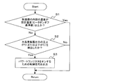
- the temperature control unit 70 is designed so that the operation of the temperature control unit 70 follows the flow shown in FIG. An example of the operation of the temperature control unit 70 will be described using the flow shown in FIG. First, the temperature control unit 70 determines whether or not the temperature inside the thermostatic chamber 20 is equal to or higher than a set temperature (heater on / off reference value) (step S1).
- Step S2 when it is determined that the temperature inside the constant temperature bath 20 is equal to or higher than the set temperature (Yes route of step S1), the process proceeds to step S1 again. On the other hand, if it is determined that the temperature inside the thermostat 20 is lower than the set temperature (No route of step S1), it is then determined whether the rising or falling of the inverted output of the crystal oscillator 30 is detected. (Step S2).
- step S3 when the rise or fall of the inverted output of the crystal oscillator 30 cannot be detected (No route of step S2), the process proceeds to step S1 again.
- a control signal for turning on the switching element is output (step S3).
- the delay unit 80 can also be realized by a CPU, FPGA, or the like, similar to the temperature control unit 70. Even when both or one of the temperature control unit 70 and the delay unit 80 is realized by a CPU, FPGA, or the like, the heater 40 causes the fall (or rise) of the inverted output C of the crystal oscillator 30 as in the timing chart of FIG. ) At the timing of the falling (or rising) of the inverted output C of the crystal oscillator 30.
- the power transistor by causing the power transistor to perform a switching operation as the switching element 60, it is possible to apply strong derating, and the reliability can be further improved. Further, since strong derating can be applied, a small element or an inexpensive element can be used for the switching element 60.
- the timing when the heater 40 is turned on and when the heater 40 is turned off coincident with the rise or fall of the output of the crystal oscillator 30, it is possible to suppress the generation of noise when the heater 40 is turned on and off. Since the generation of jitter and the like in the oscillation output can be suppressed, it is possible to further contribute to the improvement of high reliability. Further, since the generation of noise when the heater 40 is turned on and off can be suppressed, it is not necessary to arrange a capacitor having a large capacity in parallel with the heater 40, and the apparatus can be downsized.
- the set temperature detection circuit 71 outputs a control signal corresponding to the output of the temperature detection element 50, temperature control can be performed without providing hysteresis for the on / off temperature.
- the inside of the thermostatic chamber 20 with the crystal oscillator 30 is usually kept at 80 to 90 ° C., for example.
- the lifetime L of the semiconductor element can be obtained by the following equation (1).
- Equation (1) becomes It can be expressed.
- L25 is expressed by the following equation (3) by using the Arrhenius law.
- L90 is expressed by the following equation (4).
- FIG. 5 is a diagram illustrating an example of the configuration of the temperature control device 10a of the thermostatic chamber with a crystal oscillator according to the first modification.
- the temperature control device 10a of the thermostatic chamber with a crystal oscillator shown in FIG. 5 exemplarily shows the thermostatic chamber 20, the crystal oscillator 30, the heater 40, the temperature detecting element 50, and the thermostatic chamber 20 arranged inside the thermostatic chamber 20.
- each component having the above-described reference numeral has the same function as each component described above, and thus detailed description thereof is omitted.
- the switching element 60a controls on / off of the heater 40 by switching.
- a MOSFET is used as an example. Therefore, the drain of the MOSFET is connected to the heater 40, the source is grounded, and the control signal output from the delay unit 80 is input to the gate as an applied voltage. That is, the switching element 60a functions as an example of a switching element that performs on / off control of the heater.
- the temperature control unit 70 and the delay unit 80 can be realized by a CPU, FPGA, or the like.
- the temperature control devices 10 and 10a of the thermostatic chamber with a crystal oscillator shown in FIGS. 2 and 5 described above can be applied to, for example, a wireless transmission device.
- FIG. 6 is a diagram illustrating a configuration example applied to a wireless transmission device. 6 is illustratively a modulation / coding unit 101, a D / A conversion unit 102, a frequency conversion unit 103, a transmission antenna 104, and a temperature control device for a thermostatic chamber with a crystal oscillator. 10 or 10a.
- each component having the above-described reference numeral has the same function as each component described above, and a detailed description thereof will be omitted.
- Modulation / encoding section 101 performs predetermined modulation processing and encoding processing on transmission data, and outputs the result to D / A conversion section 102.
- the D / A conversion unit 102 converts the digital signal output from the modulation / coding unit 101 into an analog signal.
- the D / A conversion unit 102 appropriately divides and multiplies the crystal oscillator output of the temperature control device 10 (10a) of the thermostatic chamber with a crystal oscillator when performing conversion processing into an analog signal, and uses it as a clock.
- the frequency conversion unit 103 up-converts the analog signal output from the D / A conversion unit to a radio frequency. In the up-conversion, the frequency conversion unit 103 appropriately divides and multiplies the crystal oscillator output of the temperature control device 10 (10a) of the thermostatic chamber with a crystal oscillator and uses it as a local oscillation frequency.
- the transmission antenna 104 transmits the signal output from the frequency conversion unit 103.
- the modulation / coding unit 101, the D / A conversion unit 102, the frequency conversion unit 103, and the transmission antenna 104 are operated by the oscillation signal from the crystal oscillator 30 in the temperature control device 10 or 10a of the thermostat with crystal oscillator. It functions as an example of a unit. According to the above configuration, the wireless transmission device 100 can stably perform transmission processing without being affected by the environmental temperature.
- the power consumption of the apparatus 10 (10a) can be significantly reduced as compared with the conventional example, and thus the power consumption of the transmission apparatus 100 to which the apparatus 10 (10a) is applied can be greatly reduced. Furthermore, since this apparatus 10 (10a) can improve reliability more than a prior art example, the transmission apparatus 100 which applied this can also improve reliability.
- the transmission device 100 to which the device 10 (10a) is applied can be manufactured at a low cost and in a small size. 100 degrees of design freedom can be improved. Furthermore, since the device 10 (10a) can suppress noise when the heater is turned on and off, the transmission device 100 to which the device 10 (10a) is applied can obtain a stable output.
- FIG. 7 is a diagram illustrating a configuration example applied to a wireless reception device. 7 exemplarily includes a receiving antenna 201, a frequency conversion unit 102, an A / D conversion unit 203, a demodulation / decoding unit 204, and a temperature control device 10 for a thermostatic chamber with a crystal oscillator. Alternatively, 10a is provided.
- the frequency converter 202 down-converts the radio signal received by the receiving antenna 201 from a radio frequency to an intermediate frequency.
- the frequency conversion unit 202 appropriately divides and multiplies the crystal oscillator output of the temperature control device 10 (10a) of the above-described thermostatic chamber with crystal oscillator at the time of down-conversion, and uses it as a local oscillation frequency.
- the A / D conversion unit 203 performs sampling processing on the signal output from the frequency conversion unit 203 and converts the signal into a digital signal.
- the A / D conversion unit 203 appropriately divides and multiplies the crystal oscillator output of the temperature control device 10 (10a) of the above-described thermostatic chamber with crystal oscillator and uses it as a clock.
- the demodulation / decoding unit 204 extracts the transmitted data by performing demodulation processing and decoding processing on the digital signal output from the A / D conversion unit 203. That is, the reception antenna 201, the frequency conversion unit 102, the A / D conversion unit 203, and the demodulation / decoding unit 204 are operated by an oscillation signal from the crystal oscillator 30 in the temperature control device 10 or 10a of the thermostatic chamber with a crystal oscillator. Functions as an example.
- the wireless reception device 200 can stably perform reception processing without being affected by the environmental temperature. Further, as described above, the power consumption of the apparatus 10 (10a) can be greatly reduced as compared with the conventional example, and thus the power consumption of the receiving apparatus 200 to which the apparatus 10 (10a) is applied can be greatly reduced.
- this apparatus 10 (10a) can improve reliability more than a prior art example, the receiving apparatus 200 to which this apparatus 10 is applied can also improve reliability.
- the device 10 (10a) can use a small element or an inexpensive element as a switching element, the receiving device 200 to which the device 10 (10a) is applied can be manufactured at a low cost and in a small size. The degree of freedom in designing 200 can be improved.
- the present apparatus 10 (10a) can suppress noise when the heater is turned on / off, the receiving apparatus 200 to which this is applied can obtain a stable output.
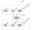
- the wireless transmission / reception device 300 may be configured by sharing the temperature control device 10 or 10a of the thermostat with crystal oscillator between the wireless transmission device 100a and the wireless reception device 200a.
- the detailed description is abbreviate
- the same effects as those of the first application example and the second application example described above can be obtained. Further, if the device 10 (10a) is shared by the wireless transmission device 100a and the wireless reception device 200a, the configuration can be further simplified. [6] Others The configurations and functions of the temperature control devices 10 and 10a of the above-described thermostatic chamber with crystal oscillator, the wireless transmission device 100, the wireless reception device 200, and the wireless transmission / reception device 300 are selected as necessary. It may be used in combination as appropriate. In other words, the above-described configurations and functions may be selected or used in appropriate combination so that the functions of the present invention can be exhibited.
- the base station in the wireless communication system is appropriately used by using the respective configurations and functions of the temperature control devices 10 and 10a of the thermostatic chamber with the crystal oscillator, the wireless transmission device 100, the wireless reception device 200, and the wireless transmission / reception device 300 as appropriate. Can be configured. Furthermore, in the above-described embodiment, the example in which the output of the crystal oscillator 30 is inverted and input to the temperature control unit 70 has been described, but an output that is not inverted can also be input to the temperature control unit 70.
- the output of the crystal oscillator 30 may be appropriately divided and multiplied before being input to the temperature control unit 70.
Landscapes
- Oscillators With Electromechanical Resonators (AREA)
Abstract
発振信号を出力する水晶発振器(30)を内部に有する恒温槽(20)と、恒温槽(20)内部を加温するヒータ(40)と、恒温槽(20)内部の温度を検出する温度検出部(50)と、ヒータ(40)のオンオフ制御を行なうスイッチング素子(60)と、温度検出部(50)からの検出結果及び水晶発振器(30)からの発振信号を受けて、発振信号に同期して、スイッチング素子(60)をオンオフ制御する温度制御部(70)とをそなえる。
Description
本件は、水晶発振器付き恒温槽の温度制御装置、無線送信装置、無線受信装置、無線送受信装置及び無線基地局に関する。
環境温度に影響されにくく、安定した周波数特性をそなえた水晶発振器として、恒温槽付き水晶発振器(OCXO;Oven Controlled Crystal Oscillator)が知られている。
この恒温槽付き水晶発振器は、水晶発振器としての水晶振動子を、温度が一定に保たれたケースである恒温槽の中に搭載したものである。
図1は、従来装置の構成の一例を示す図である。
この恒温槽付き水晶発振器は、水晶発振器としての水晶振動子を、温度が一定に保たれたケースである恒温槽の中に搭載したものである。
図1は、従来装置の構成の一例を示す図である。
図1に例示する従来装置は、恒温槽2の内部に、水晶発振器3と、恒温槽2内の温度を制御するための電気ヒータ(以下、単に「ヒータ」という)4,温度検出素子5,パワートランジスタ6,抵抗7及びコンデンサ8とをそなえる。
即ち、図1に例示する従来装置は、恒温槽2の内部の温度を一定に保つため、温度検出素子5によって検出された恒温槽2の内部温度に基づき、パワートランジスタ6のコレクタ電圧を変化させることにより、ヒータ4の両端にかかる電圧を調整する。
即ち、図1に例示する従来装置は、恒温槽2の内部の温度を一定に保つため、温度検出素子5によって検出された恒温槽2の内部温度に基づき、パワートランジスタ6のコレクタ電圧を変化させることにより、ヒータ4の両端にかかる電圧を調整する。
抵抗7及びコンデンサ8は、ヒータ4による急峻なスイッチングを避けるため、ヒータ4に流れる電流の変化を緩やかにする働きをする。
図1に示す構成によると、パワートランジスタ6において電力損失が生じ、熱が発生するため、パワートランジスタ6で発生する熱を有効利用すべく、パワートランジスタ6は、恒温槽2の内部に配置され使用される(下記特許文献1参照)。
図1に示す構成によると、パワートランジスタ6において電力損失が生じ、熱が発生するため、パワートランジスタ6で発生する熱を有効利用すべく、パワートランジスタ6は、恒温槽2の内部に配置され使用される(下記特許文献1参照)。
しかしながら、図1に例示する従来装置では、ヒータ4と並列に接続されるコンデンサ8によって、抵抗値の小さいヒータ4に流れる電流の変化を緩やかにするためには、コンデンサ8の容量を大きくしなければならない。そのため、コンデンサ8自体のサイズも大きくなり、装置の小型化が難しいという欠点があった。
また、図1に例示する従来装置では、恒温槽2の内部は高温に保たれているため、パワートランジスタ6を恒温槽2の内部に配置すると、パワートランジスタ6に温度ストレスがかかってしまい、信頼性が劣化する。
また、図1に例示する従来装置では、恒温槽2の内部は高温に保たれているため、パワートランジスタ6を恒温槽2の内部に配置すると、パワートランジスタ6に温度ストレスがかかってしまい、信頼性が劣化する。
そこで、本件は、小型で信頼性の高い水晶発振器付き恒温槽の温度制御装置を提供することを目的の1つとする。
なお、前記目的に限らず、後述する発明を実施するための形態に示す各構成により導かれる作用効果であって、従来の技術によっては得られない作用効果を奏することも本発明の他の目的の一つとして位置付けることができる。
なお、前記目的に限らず、後述する発明を実施するための形態に示す各構成により導かれる作用効果であって、従来の技術によっては得られない作用効果を奏することも本発明の他の目的の一つとして位置付けることができる。
(1)第1の案として、発振信号を出力する水晶発振器を内部に有する恒温槽と、該恒温槽内部を加温するヒータと、該恒温槽内部の温度を検出する温度検出部と、該ヒータのオンオフ制御を行なうスイッチング素子と、該温度検出部からの検出結果及び該水晶発振器からの発振信号を受けて、該発振信号に同期して、該スイッチング素子をオンオフ制御する温度制御部とをそなえて構成される水晶発振器付き恒温槽の温度制御装置を用いることができる。
(2)また、第2の案として、上記の水晶発振器付き恒温槽の温度制御装置における該水晶発振器からの発振信号で作動する送信部をそなえた無線送信装置を用いることができる。
(3)さらに、第3の案として、上記の水晶発振器付き恒温槽の温度制御装置における該水晶発振器からの発振信号で作動する受信部をそなえた無線受信装置を用いることができる。
(3)さらに、第3の案として、上記の水晶発振器付き恒温槽の温度制御装置における該水晶発振器からの発振信号で作動する受信部をそなえた無線受信装置を用いることができる。
(4)また、第4の案として、上記無線送信装置と、上記無線受信装置とそなえた無線送受信装置を用いることができる。
(5)さらに、第5の案として、上記の水晶発振器付き恒温槽の温度制御装置を有する無線基地局を用いることができる。
(5)さらに、第5の案として、上記の水晶発振器付き恒温槽の温度制御装置を有する無線基地局を用いることができる。
小型で信頼性の高い水晶発振器付き恒温槽の温度制御装置を提供することが可能となる。
以下、図面を参照して本発明の実施の形態を説明する。ただし、以下に示す実施の形態は、あくまでも例示に過ぎず、以下に示す各実施形態及び変形例で明示しない種々の変形や技術の適用を排除する意図はない。即ち、各実施形態及び変形例を、本発明の趣旨を逸脱しない範囲で種々変形して実施できることはいうまでもない。
〔1〕一実施形態
(1.1)水晶発振器付き恒温槽の温度制御装置の構成
図2は、一実施形態に係る水晶発振器付き恒温槽の温度制御装置(以下、適宜「本装置」ということがある)の構成の一例を示す図である。
〔1〕一実施形態
(1.1)水晶発振器付き恒温槽の温度制御装置の構成
図2は、一実施形態に係る水晶発振器付き恒温槽の温度制御装置(以下、適宜「本装置」ということがある)の構成の一例を示す図である。
この水晶発振器付き恒温槽の温度制御装置10は、例示的に、恒温槽20と、恒温槽20の内部に配置される水晶発振器30,電気ヒータ(以下、単に「ヒータ」という)40及び温度検出素子50と、恒温槽20の外部に配置されるスイッチング素子60,温度制御部70,遅延部80及びNOT回路91,92とをそなえる。
恒温槽20は、内部の温度を一定に保つケースであり、金属製の筐体や保温材などで保温層を施すことによって構成される。即ち、恒温槽20は、発振信号を出力する水晶発振器30を内部に有する恒温槽の一例として機能する。
恒温槽20は、内部の温度を一定に保つケースであり、金属製の筐体や保温材などで保温層を施すことによって構成される。即ち、恒温槽20は、発振信号を出力する水晶発振器30を内部に有する恒温槽の一例として機能する。
水晶発振器30は、電源端子(Vcc)に接続され、周囲温度に依存した周波数の発振信号を出力する。水晶発振器30から出力された発振信号は、NOT回路91を介して温度制御部70に出力され、NOT回路91及び92を介して外部に出力される。
ヒータ40は、電源端子(Vcc)に接続され、恒温槽40の内部の温度が低下すると熱を発生し、恒温槽20の内部を加温する。なお、ヒータ40のオンオフは、後述するスイッチング素子60によって制御される。即ち、ヒータ40は、恒温槽20内部を加温するヒータの一例として機能する。
ヒータ40は、電源端子(Vcc)に接続され、恒温槽40の内部の温度が低下すると熱を発生し、恒温槽20の内部を加温する。なお、ヒータ40のオンオフは、後述するスイッチング素子60によって制御される。即ち、ヒータ40は、恒温槽20内部を加温するヒータの一例として機能する。
温度検出素子50は、恒温槽20の内部の温度を検出し、検出した温度に応じたレベルの信号を出力するものであり、サーミスタなどの温度依存性の特性を有する素子を用いることができる。即ち、温度検出素子50は、恒温槽20内部の温度を検出する温度検出部の一例として機能する。
スイッチング素子60は、ヒータ40のオンオフをスイッチングにより制御するものであり、本例では、パワートランジスタを用いる。
スイッチング素子60は、ヒータ40のオンオフをスイッチングにより制御するものであり、本例では、パワートランジスタを用いる。
このため、パワートランジスタのコレクタをヒータ40に接続し、エミッタを接地し、ベースには後述する遅延部80から出力された制御信号を入力する。
即ち、スイッチング素子60は、ヒータ40のオンオフ制御を行なうスイッチング素子の一例として機能する。
一般的に、水晶発振器30の出力のノイズは発振出力の立上がり、立下がりで発生することが知られている。
即ち、スイッチング素子60は、ヒータ40のオンオフ制御を行なうスイッチング素子の一例として機能する。
一般的に、水晶発振器30の出力のノイズは発振出力の立上がり、立下がりで発生することが知られている。
また、ヒータ40のオンオフ時には大きな電流が流れるため、電源電圧が揺らぎ、発振出力にノイズが発生する。さらに、このノイズは、発振出力におけるジッタなどの原因となる。
温度制御部70は、ヒータ40のオンオフのタイミングを制御することにより、この二つのノイズの発生タイミングを同期させ、ヒータ40オンオフ時のノイズ発生を抑制するものである。
温度制御部70は、ヒータ40のオンオフのタイミングを制御することにより、この二つのノイズの発生タイミングを同期させ、ヒータ40オンオフ時のノイズ発生を抑制するものである。
即ち、温度制御部70は、水晶発振器30及び温度検出素子50の出力に基づき、ヒータ40のオンオフを制御するための制御信号を出力する。
このため、温度制御部70は、設定温度検出回路71及び同期回路72をそなえる。
設定温度検出回路71は、温度検出素子50の出力に基づき、ヒータ40をオン状態にするための信号を出力する。
このため、温度制御部70は、設定温度検出回路71及び同期回路72をそなえる。
設定温度検出回路71は、温度検出素子50の出力に基づき、ヒータ40をオン状態にするための信号を出力する。
例えば、設定温度検出回路71は、温度検出素子50の出力に対応する温度が、ヒータ40のオンオフの切り替えの基準となる値(以下、ヒータオンオフ基準値ともいう)より低下したか否かを判断し、温度検出素子50の出力に対応する温度がヒータオンオフ基準値より低下したと判断すると、ヒータ40をオンするための信号を出力し、温度検出素子50の出力に対応する温度がヒータオンオフ基準値以上であると判断すると、ヒータ40をオンするための信号を出力しない。
即ち、設定温度検出回路71は、温度検出部の一例である温度検出素子50からの検出結果を受け、恒温槽20内部の温度とヒータオンオフ基準値との比較結果としてのオンオフ信号を出力する比較部の一例として機能する。
なお、温度検出素子50は、バイメタルを用いたサーマルリレーのように、検出した温度に応じて出力のオンオフを切り替える素子を用いることも可能である。
なお、温度検出素子50は、バイメタルを用いたサーマルリレーのように、検出した温度に応じて出力のオンオフを切り替える素子を用いることも可能である。
このように、温度検出素子50を、バイメタルを用いたサーマルリレーなどによって構成することにより、温度検出素子50自体がオンオフを切り替えて出力する場合には、設定温度検出回路71を省略することができる。
同期回路72は、設定温度検出回路71の出力を水晶発振器30の発振信号に同期させる。即ち、同期回路72は、比較部の一例である設定温度検出回路71からのオンオフ信号と水晶発振器30からの発振信号とを受けて、発振信号に同期して、スイッチング素子60をオンオフ制御する制御信号を生成する同期部の一例として機能する。
同期回路72は、設定温度検出回路71の出力を水晶発振器30の発振信号に同期させる。即ち、同期回路72は、比較部の一例である設定温度検出回路71からのオンオフ信号と水晶発振器30からの発振信号とを受けて、発振信号に同期して、スイッチング素子60をオンオフ制御する制御信号を生成する同期部の一例として機能する。
本実施形態では、同期回路72の一例として、D型フリップフロップを用いる。即ち、同期回路72は、NAND回路721~728及びNOT回路729,730をそなえたD型フリップフロップとして構成することができる。
この同期回路72は、そのD型フリップフロップ機能により、設定温度検出回路71がヒータ40をオンする信号を出力しているときに、水晶発振器30からの反転出力が立上がると、ヒータ40をオンするための制御信号を出力し、設定温度検出回路71が、ヒータ40をオンする信号の出力を止めたあと、水晶発振器30からの反転出力が立上がると、ヒータ40をオフするための制御信号に切り替えるようになっている。
この同期回路72は、そのD型フリップフロップ機能により、設定温度検出回路71がヒータ40をオンする信号を出力しているときに、水晶発振器30からの反転出力が立上がると、ヒータ40をオンするための制御信号を出力し、設定温度検出回路71が、ヒータ40をオンする信号の出力を止めたあと、水晶発振器30からの反転出力が立上がると、ヒータ40をオフするための制御信号に切り替えるようになっている。
即ち、温度制御部70は、温度検出部の一例である温度検出素子50からの検出結果及び水晶発振器30からの発振信号を受けて、発振信号に同期して、スイッチング素子60をオンオフ制御する温度制御部の一例として機能する。
遅延部80は、温度制御部70から出力された信号を遅延させることにより、スイッチング素子60のオンオフのタイミングの微調整を行なう。
遅延部80は、温度制御部70から出力された信号を遅延させることにより、スイッチング素子60のオンオフのタイミングの微調整を行なう。
例えば、温度制御部70において信号の遅延が発生し、水晶発振器20の立上がりまたは立下がりのタイミングと、ヒータ40のオンオフのタイミングとの間にずれが生じるような場合、遅延部80は、温度制御部70から出力された制御信号を遅延させることにより、タイミングの微調整を行なう。
このため、遅延部80は、例示的に、可変抵抗81と、コンデンサ82とをそなえる。
このため、遅延部80は、例示的に、可変抵抗81と、コンデンサ82とをそなえる。
遅延部80は、可変抵抗81を調整することにより、スイッチング素子60に入力される制御信号を遅延させる。
これにより、スイッチング素子60のオンオフのタイミングを調整することができ、その結果、ヒータ40のオンオフのタイミングと、水晶発振器30の立上がりまたは立下がりのタイミングとを完全に一致させることができる。
これにより、スイッチング素子60のオンオフのタイミングを調整することができ、その結果、ヒータ40のオンオフのタイミングと、水晶発振器30の立上がりまたは立下がりのタイミングとを完全に一致させることができる。
また、水晶発振器30から出力されるノイズが最小となるように、可変抵抗81を調整してもよい。
即ち、遅延部80は、温度制御部70からの制御信号を遅延させてスイッチング素子に入力する遅延部の一例として機能し得る。
また、温度制御部70により、ヒータ40のオンオフのタイミングと、水晶発振器20の立上がりまたは立下がりのタイミングとを十分に同期させられる場合には、遅延部80を省略することもできる。
即ち、遅延部80は、温度制御部70からの制御信号を遅延させてスイッチング素子に入力する遅延部の一例として機能し得る。
また、温度制御部70により、ヒータ40のオンオフのタイミングと、水晶発振器20の立上がりまたは立下がりのタイミングとを十分に同期させられる場合には、遅延部80を省略することもできる。
(1.2)水晶発振器付き恒温槽の温度制御装置の動作
図3を用いて、本装置10による温度制御の動作の一例を説明する。
図3は、設定温度検出回路71の出力(図2中の点D参照),水晶発振器30の反転出力(図2中の点C参照),温度制御部70の出力(図2中の点Q参照),スイッチング素子60の入力(図2中の点B参照)及びヒータ30の入力(図2中の点A参照)を時系列で並べて示すタイムチャートである。
図3を用いて、本装置10による温度制御の動作の一例を説明する。
図3は、設定温度検出回路71の出力(図2中の点D参照),水晶発振器30の反転出力(図2中の点C参照),温度制御部70の出力(図2中の点Q参照),スイッチング素子60の入力(図2中の点B参照)及びヒータ30の入力(図2中の点A参照)を時系列で並べて示すタイムチャートである。
恒温槽20の内部の温度がヒータオンオフ基準値より低くなると、設定温度検出回路71の出力Dがハイレベルとなる(図3の時間t0参照)。
しかしながら、この時点では、温度制御部70の出力Qはハイレベルとはならず、ヒータ40はオンとならない。
水晶発振器30の反転出力Cの次の立上がりのタイミング(図3の時間t1参照)で、温度制御部70の出力Qがハイレベルとなる。
しかしながら、この時点では、温度制御部70の出力Qはハイレベルとはならず、ヒータ40はオンとならない。
水晶発振器30の反転出力Cの次の立上がりのタイミング(図3の時間t1参照)で、温度制御部70の出力Qがハイレベルとなる。
スイッチング素子60の入力電位Bは、遅延部80の影響により、緩やかに上昇する。
そして、例えば、水晶発振器30の反転出力Cの次の立下がりのタイミング(図3の時間t2参照)で、スイッチング素子60の入力電位Bが、スイッチング素子60がオンになる電位に達する。
これにより、水晶発振器30の反転出力Cの立下がりのタイミングにヒータ40がオンとなり、ヒータ40がオンとなるタイミングが、水晶発振器30の反転出力Cの立下がりに一致する。
そして、例えば、水晶発振器30の反転出力Cの次の立下がりのタイミング(図3の時間t2参照)で、スイッチング素子60の入力電位Bが、スイッチング素子60がオンになる電位に達する。
これにより、水晶発振器30の反転出力Cの立下がりのタイミングにヒータ40がオンとなり、ヒータ40がオンとなるタイミングが、水晶発振器30の反転出力Cの立下がりに一致する。
なお、上述した例では、スイッチング素子60がオン状態になるタイミングが、水晶発振器30の反転出力Cの立下がりのタイミング(t2)に一致するように遅延部80を調整したが、t2以降に生じる水晶発振器30の反転出力Cの立上がりや立下がりのタイミング(例えば、図3の時間t3や時間t4など)に一致するように遅延部80を調整しても良い。
次に、恒温槽20の内部の温度がヒータオンオフ基準値以上になると、設定温度検出回路71の出力Dがローレベルとなる(図3の時間t5参照)。
しかしながら、この時点では、温度制御部70の出力Qはローレベルとはならず、ヒータ40はオフとならない。
水晶発振器30の反転出力Cの次の立上がりのタイミング(図3の時間t6参照)で、温度制御部70の出力Qがローレベルとなる。
しかしながら、この時点では、温度制御部70の出力Qはローレベルとはならず、ヒータ40はオフとならない。
水晶発振器30の反転出力Cの次の立上がりのタイミング(図3の時間t6参照)で、温度制御部70の出力Qがローレベルとなる。
スイッチング素子60の入力電位Bは、遅延部80の影響により、緩やかに低下する。
そして、例えば、水晶発振器30の反転出力Cの次の立下がりのタイミング(図3の時間t7参照)で、スイッチング素子60の入力電位Bが、スイッチング素子60がオフ状態になる電位に達する。
これにより、水晶発振器30の反転出力Cの立下がりのタイミングにヒータ40がオフとなり、ヒータ40がオフとなるタイミングが水晶発振器30の反転出力Cの立下がりに一致する。
そして、例えば、水晶発振器30の反転出力Cの次の立下がりのタイミング(図3の時間t7参照)で、スイッチング素子60の入力電位Bが、スイッチング素子60がオフ状態になる電位に達する。
これにより、水晶発振器30の反転出力Cの立下がりのタイミングにヒータ40がオフとなり、ヒータ40がオフとなるタイミングが水晶発振器30の反転出力Cの立下がりに一致する。
なお、上述した例では、スイッチング素子60がオフ状態になるタイミングが、水晶発振器30の反転出力Cの立下がりのタイミング(t7)に一致するように遅延部80を調整したが、t6以降に生じる水晶発振器30の反転出力Cの立上がりや立下がりのタイミングに一致するように遅延部80を調整しても良い。
(1.3)温度制御部,遅延部の変形例
なお、上記の温度制御部70は、例えば、CPU(Central Processing Unit)やFPGA(Field Programmable Gate Array)などによって実現することもできる。
(1.3)温度制御部,遅延部の変形例
なお、上記の温度制御部70は、例えば、CPU(Central Processing Unit)やFPGA(Field Programmable Gate Array)などによって実現することもできる。
この場合、温度制御部70の動作が図4に示すフローに従うように、温度制御部70を設計する。
温度制御部70の動作の一例を、図4に示すフローを用いて説明する。
まず、温度制御部70は、恒温槽20の内部の温度が設定温度(ヒータオンオフ基準値)以上であるか否かを判断する(ステップS1)。
温度制御部70の動作の一例を、図4に示すフローを用いて説明する。
まず、温度制御部70は、恒温槽20の内部の温度が設定温度(ヒータオンオフ基準値)以上であるか否かを判断する(ステップS1)。
ここで、恒温槽20の内部の温度が設定温度以上であると判断した場合には(ステップS1のYesルート)、再度ステップS1に移行する。
一方、恒温槽20の内部の温度が設定温度より低いと判断した場合には(ステップS1のNoルート)、次に、水晶発振器30の反転出力の立上がりまたは立下がりを検出したか否かを判断する(ステップS2)。
一方、恒温槽20の内部の温度が設定温度より低いと判断した場合には(ステップS1のNoルート)、次に、水晶発振器30の反転出力の立上がりまたは立下がりを検出したか否かを判断する(ステップS2)。
ここで、水晶発振器30の反転出力の立上がりまたは立下がりを検出できない場合には(ステップS2のNoルート)、再度ステップS1に移行する。
一方、水晶発振器30の反転出力の立上がりまたは立下がりを検出した場合には(ステップS2のYesルート)、スイッチング素子をオンするための制御信号を出力する(ステップS3)。
一方、水晶発振器30の反転出力の立上がりまたは立下がりを検出した場合には(ステップS2のYesルート)、スイッチング素子をオンするための制御信号を出力する(ステップS3)。
また、遅延部80も、温度制御部70と同様、CPUやFPGAなどによって実現することも可能である。
なお、温度制御部70,遅延部80の両方または一方をCPUやFPGAなどで実現した場合も、図3のタイミングチャートと同様、ヒータ40は、水晶発振器30の反転出力Cの立下がり(または立上がり)のタイミングでオンされる一方、水晶発振器30の反転出力Cの立下がり(または立上がり)のタイミングでオフされる。
なお、温度制御部70,遅延部80の両方または一方をCPUやFPGAなどで実現した場合も、図3のタイミングチャートと同様、ヒータ40は、水晶発振器30の反転出力Cの立下がり(または立上がり)のタイミングでオンされる一方、水晶発振器30の反転出力Cの立下がり(または立上がり)のタイミングでオフされる。
(1.4)水晶発振器付き恒温槽の温度制御装置によって得られる効果
以上の構成によれば、スイッチング素子60としてパワートランジスタにスイッチング動作をさせることにより、パワートランジスタの消費電力を大幅に低減することができる。
また、消費電力の低減に伴い、発熱が抑えられ、パワートランジスタを恒温槽20の外部に配置することができるため、パワートランジスタの信頼性を向上することができる。
以上の構成によれば、スイッチング素子60としてパワートランジスタにスイッチング動作をさせることにより、パワートランジスタの消費電力を大幅に低減することができる。
また、消費電力の低減に伴い、発熱が抑えられ、パワートランジスタを恒温槽20の外部に配置することができるため、パワートランジスタの信頼性を向上することができる。
さらに、スイッチング素子60としてパワートランジスタにスイッチング動作をさせることにより、強いディレーティングをかけることが可能になり、信頼性を更に改善することができる。
また、強いディレーティングをかけることが可能であるため、スイッチング素子60に小型な素子や安価な素子を用いることができる。
また、強いディレーティングをかけることが可能であるため、スイッチング素子60に小型な素子や安価な素子を用いることができる。
さらに、ヒータ40がオンとなるタイミング及びオフとなるタイミングを、水晶発振器30の出力の立上がりまたは立下りに一致させることにより、ヒータ40のオンオフ時のノイズの発生を抑制することができ、更には、発振出力におけるジッタなどの発生を抑えることができるため、高い信頼性の向上に更に寄与することができる。
また、ヒータ40のオンオフ時のノイズの発生が抑制できるため、ヒータ40に並列して容量の大きなコンデンサを配置する必要がなくなり、装置の小型化が可能になる。
また、ヒータ40のオンオフ時のノイズの発生が抑制できるため、ヒータ40に並列して容量の大きなコンデンサを配置する必要がなくなり、装置の小型化が可能になる。
さらに、設定温度検出回路71が、温度検出素子50の出力に対応して制御信号を出力するので、オンオフの温度にヒステリシスを設けることなく温度制御ができる。
ここで、以上の構成により、パワートランジスタの信頼性をどれだけ改善できるかを説明する。
通常、水晶発振器30付き恒温槽20の内部は、例えば、80~90℃に保たれることが普通である。
ここで、以上の構成により、パワートランジスタの信頼性をどれだけ改善できるかを説明する。
通常、水晶発振器30付き恒温槽20の内部は、例えば、80~90℃に保たれることが普通である。
そこで、環境温度が、例えば25℃から90℃に変わった場合のパワートランジスタの故障率の変化量を検証する。
温度ストレスによる半導体素子の寿命を予測する法則として、アレニウスの法則がある。アレニウスの法則によると、半導体素子の寿命Lを下記の(1)式で求めることができる。

温度ストレスによる半導体素子の寿命を予測する法則として、アレニウスの法則がある。アレニウスの法則によると、半導体素子の寿命Lを下記の(1)式で求めることができる。
ただし、Aは所定の定数、Eaは活性化エネルギー(半導体の活性化エネルギーは1.2[eV]程度)、Tは絶対温度、kはボルツマン定数である。
ここで、

とすると、(1)式は

と表せる。
ここで、
次に、周囲温度が25℃(298K)の時の半導体素子の寿命をL25とすると、アレニウスの法則を用いることにより、L25は以下の(3)式で表わされる

同様に、周囲温度が90℃(363K)の時の半導体素子の寿命をL90とすると、L90は以下の(4)式で表わされる。

そして、上記(3)式及び(4)式を用いて、周囲温度が25℃の時と90℃の時との半導体素子の寿命を比較すると、

となる。
したがって、環境温度が、上記のように例えば25℃から90℃へ上昇することにより、故障設計FIT数は約4506倍に悪化する。
以上から、一実施形態に係る恒温槽付き水晶発振器を用いることにより、信頼性を大幅に改善できることが理解できる。
したがって、環境温度が、上記のように例えば25℃から90℃へ上昇することにより、故障設計FIT数は約4506倍に悪化する。
以上から、一実施形態に係る恒温槽付き水晶発振器を用いることにより、信頼性を大幅に改善できることが理解できる。
〔2〕第1変形例
上述した実施形態では、スイッチング素子60としてパワートランジスタを用いる例について説明したが、例えば、パワートランジスタに代えて他の半導体素子を用いることもできる。
図5は、第1変形例に係る水晶発振器付き恒温槽の温度制御装置10aの構成の一例を示す図である。
上述した実施形態では、スイッチング素子60としてパワートランジスタを用いる例について説明したが、例えば、パワートランジスタに代えて他の半導体素子を用いることもできる。
図5は、第1変形例に係る水晶発振器付き恒温槽の温度制御装置10aの構成の一例を示す図である。
図5に示す水晶発振器付き恒温槽の温度制御装置10aは、例示的に、恒温槽20と、恒温槽20の内部に配置される水晶発振器30,ヒータ40及び温度検出素子50と、恒温槽20の外部に配置されるスイッチング素子60a,抵抗61,温度制御部70,遅延部80及びNOT回路91,92とをそなえる。なお、図5中、既述の符号を付した各構成については、前述の各構成と同様の機能を具備するので、その詳細な説明は省略する。
スイッチング素子60aは、ヒータ40のオンオフをスイッチングにより制御するものであり、本例では、一例として、MOSFETを用いる。
このため、MOSFETのドレインをヒータ40に接続し、ソースを接地し、ゲートには遅延部80から出力された制御信号を印加電圧として入力する。
即ち、スイッチング素子60aは、ヒータのオンオフ制御を行なうスイッチング素子の一例として機能する。
このため、MOSFETのドレインをヒータ40に接続し、ソースを接地し、ゲートには遅延部80から出力された制御信号を印加電圧として入力する。
即ち、スイッチング素子60aは、ヒータのオンオフ制御を行なうスイッチング素子の一例として機能する。
以上の構成によると、スイッチング素子60aに、MOSFETを用いた場合でも、上述した一実施形態の場合と同様の効果が得られる。
なお、この図5に示す例でも、温度制御部70や遅延部80をCPUやFPGAなどで実現できることはいうまでもない。
〔3〕本装置の第1適用例
上述した図2や図5で示す水晶発振器付き恒温槽の温度制御装置10,10aは、例えば、無線送信装置に適用することができる。
なお、この図5に示す例でも、温度制御部70や遅延部80をCPUやFPGAなどで実現できることはいうまでもない。
〔3〕本装置の第1適用例
上述した図2や図5で示す水晶発振器付き恒温槽の温度制御装置10,10aは、例えば、無線送信装置に適用することができる。
図6は、無線送信装置に適用した構成例を示す図である。
図6に示す無線送信装置100は、例示的に、変調・符号化部101と、D/A変換部102と、周波数変換部103と、送信アンテナ104と、水晶発振器付き恒温槽の温度制御装置10あるいは10aとをそなえる。
なお、図6中、既述の符号を付した各構成については、前述の各構成と同様の機能を具備するので、その詳細な説明は省略する。
図6に示す無線送信装置100は、例示的に、変調・符号化部101と、D/A変換部102と、周波数変換部103と、送信アンテナ104と、水晶発振器付き恒温槽の温度制御装置10あるいは10aとをそなえる。
なお、図6中、既述の符号を付した各構成については、前述の各構成と同様の機能を具備するので、その詳細な説明は省略する。
変調・符号化部101は、送信データに所定の変調処理及び符号化処理を施し、D/A変換部102に出力する。
D/A変換部102は、変調・符号化部101から出力されたディジタル信号をアナログ信号へ変換する。
D/A変換部102は、アナログ信号への変換処理を施す際、水晶発振器付き恒温槽の温度制御装置10(10a)の水晶発振器出力を適宜分周,逓倍し、クロックとして用いる。
D/A変換部102は、変調・符号化部101から出力されたディジタル信号をアナログ信号へ変換する。
D/A変換部102は、アナログ信号への変換処理を施す際、水晶発振器付き恒温槽の温度制御装置10(10a)の水晶発振器出力を適宜分周,逓倍し、クロックとして用いる。
周波数変換部103は、D/A変換部から出力されたアナログ信号を、無線周波数にアップコンバートする。
周波数変換部103は、アップコンバートの際、水晶発振器付き恒温槽の温度制御装置10(10a)の水晶発振器出力を適宜分周,逓倍し、局部発振周波数として用いる。
送信アンテナ104は、周波数変換部103から出力された信号を送信する。
周波数変換部103は、アップコンバートの際、水晶発振器付き恒温槽の温度制御装置10(10a)の水晶発振器出力を適宜分周,逓倍し、局部発振周波数として用いる。
送信アンテナ104は、周波数変換部103から出力された信号を送信する。
即ち、変調・符号化部101,D/A変換部102,周波数変換部103及び送信アンテナ104は、水晶発振器付き恒温槽の温度制御装置10あるいは10aにおける水晶発振器30からの発振信号で作動する送信部の一例として機能する。
以上の構成によれば、無線送信装置100は、環境温度に影響されることなく、安定して送信処理を行なうことができる。
以上の構成によれば、無線送信装置100は、環境温度に影響されることなく、安定して送信処理を行なうことができる。
また、上述したように、本装置10(10a)は、従来例より消費電力を大幅に低減することができるため、これを適用した送信装置100の消費電力も大幅に低減することができる。
さらに、本装置10(10a)は、従来例より信頼性を向上することができるため、これを適用した送信装置100も、信頼性を向上することができる。
さらに、本装置10(10a)は、従来例より信頼性を向上することができるため、これを適用した送信装置100も、信頼性を向上することができる。
また、本装置10(10a)は、スイッチング素子に小型な素子や安価な素子を用いることができるため、これを適用した送信装置100も、安価かつ小型に製造することができ、また、送信装置100の設計の自由度を向上することができる。
さらに、本装置10(10a)は、ヒータオンオフ時のノイズを抑制することができるため、これを適用した送信装置100は、安定した出力を得ることができる。
さらに、本装置10(10a)は、ヒータオンオフ時のノイズを抑制することができるため、これを適用した送信装置100は、安定した出力を得ることができる。
〔4〕本装置の第2適用例
また、上述した図2や図5で示す水晶発振器付き恒温槽の温度制御装置10,10aは、例えば、無線受信装置に適用することができる。
図7は、無線受信装置に適用した構成例を示す図である。
図7に示す無線受信装置200は、例示的に、受信アンテナ201と、周波数変換部102と、A/D変換部203と、復調・復号部204と、水晶発振器付き恒温槽の温度制御装置10あるいは10aとをそなえる。
また、上述した図2や図5で示す水晶発振器付き恒温槽の温度制御装置10,10aは、例えば、無線受信装置に適用することができる。
図7は、無線受信装置に適用した構成例を示す図である。
図7に示す無線受信装置200は、例示的に、受信アンテナ201と、周波数変換部102と、A/D変換部203と、復調・復号部204と、水晶発振器付き恒温槽の温度制御装置10あるいは10aとをそなえる。
なお、図7中、既述の符号を付した各構成については、前述の各構成と同様の機能を具備するので、その詳細な説明は省略する。
周波数変換部202は、受信アンテナ201により受信された無線信号を、無線周波数から中間周波数にダウンコンバートする。
周波数変換部202は、ダウンコンバートの際、上述した水晶発振器付き恒温槽の温度制御装置10(10a)の水晶発振器出力を適宜分周,逓倍し、局部発振周波数として用いる。
周波数変換部202は、受信アンテナ201により受信された無線信号を、無線周波数から中間周波数にダウンコンバートする。
周波数変換部202は、ダウンコンバートの際、上述した水晶発振器付き恒温槽の温度制御装置10(10a)の水晶発振器出力を適宜分周,逓倍し、局部発振周波数として用いる。
A/D変換部203は、周波数変換部203から出力された信号に対しサンプリング処理を施し、ディジタル信号に変換する。
A/D変換部203は、サンプリング処理を施す際、上述した水晶発振器付き恒温槽の温度制御装置10(10a)の水晶発振器出力を適宜分周,逓倍し、クロックとして用いる。
A/D変換部203は、サンプリング処理を施す際、上述した水晶発振器付き恒温槽の温度制御装置10(10a)の水晶発振器出力を適宜分周,逓倍し、クロックとして用いる。
復調・復号部204は、A/D変換部203から出力されたディジタル信号に、復調処理及び復号処理を施すことにより、送信されたデータを取り出す。
即ち、受信アンテナ201,周波数変換部102,A/D変換部203及び復調・復号部204は、水晶発振器付き恒温槽の温度制御装置10あるいは10aにおける水晶発振器30からの発振信号で作動する受信部の一例として機能する。
即ち、受信アンテナ201,周波数変換部102,A/D変換部203及び復調・復号部204は、水晶発振器付き恒温槽の温度制御装置10あるいは10aにおける水晶発振器30からの発振信号で作動する受信部の一例として機能する。
以上の構成によれば、無線受信装置200は、環境温度に影響されることなく、安定して受信処理を行なうことができる。
また、上述したように、本装置10(10a)は、従来例より消費電力を大幅に低減することができるため、これを適用した受信装置200の消費電力も大幅に低減することができる。
また、上述したように、本装置10(10a)は、従来例より消費電力を大幅に低減することができるため、これを適用した受信装置200の消費電力も大幅に低減することができる。
さらに、本装置10(10a)は、従来例より信頼性を向上することができるため、これを適用した受信装置200も、信頼性を向上することができる。
また、本装置10(10a)は、スイッチング素子に小型な素子や安価な素子を用いることができるため、これを適用した受信装置200も、安価かつ小型に製造することができ、また、受信装置200の設計の自由度を向上することができる。
また、本装置10(10a)は、スイッチング素子に小型な素子や安価な素子を用いることができるため、これを適用した受信装置200も、安価かつ小型に製造することができ、また、受信装置200の設計の自由度を向上することができる。
さらに、本装置10(10a)は、ヒータオンオフ時のノイズを抑制することができるため、これを適用した受信装置200は、安定した出力を得ることができる。
〔5〕本装置の第3適用例
図6に例示した無線送信装置100と図7に例示した無線受信装置200とを組み合わせることにより、無線送受信装置を構成することができる。
〔5〕本装置の第3適用例
図6に例示した無線送信装置100と図7に例示した無線受信装置200とを組み合わせることにより、無線送受信装置を構成することができる。
また、図8に示すように、無線送信装置100aと無線受信装置200aとで、水晶発振器付き恒温槽の温度制御装置10あるいは10aを共用化することにより、無線送受信装置300を構成してもよい。
なお、図8中、既述の符号を付した各構成については、前述の各構成と同様の機能を具備するので、その詳細な説明は省略する。
なお、図8中、既述の符号を付した各構成については、前述の各構成と同様の機能を具備するので、その詳細な説明は省略する。
以上の構成によると、上述した第1適用例及び第2適用例の場合と同様の効果が得られる。
また、本装置10(10a)を無線送信装置100aと無線受信装置200aとで共用化すれば、更に構成の簡単化を達成できる。
〔6〕その他
なお、上述した水晶発振器付き恒温槽の温度制御装置10及び10a,無線送信装置100,無線受信装置200並びに無線送受信装置300の各構成及び各機能は、必要に応じて取捨選択してもよいし、適宜組み合わせて用いてもよい。即ち、本発明の機能を発揮できるように、上記の各構成及び各機能を取捨選択したり、適宜組み合わせて用いたりしてもよい。
また、本装置10(10a)を無線送信装置100aと無線受信装置200aとで共用化すれば、更に構成の簡単化を達成できる。
〔6〕その他
なお、上述した水晶発振器付き恒温槽の温度制御装置10及び10a,無線送信装置100,無線受信装置200並びに無線送受信装置300の各構成及び各機能は、必要に応じて取捨選択してもよいし、適宜組み合わせて用いてもよい。即ち、本発明の機能を発揮できるように、上記の各構成及び各機能を取捨選択したり、適宜組み合わせて用いたりしてもよい。
また、上述した水晶発振器付き恒温槽の温度制御装置10及び10a,無線送信装置100,無線受信装置200並びに無線送受信装置300の各構成及び各機能を適宜用いて、無線通信システムにおける基地局などを構成することができる。
さらに、上述した実施形態において、水晶発振器30の出力を反転して温度制御部70へ入力する例について説明したが、反転しない出力を温度制御部70へ入力することもできる。
さらに、上述した実施形態において、水晶発振器30の出力を反転して温度制御部70へ入力する例について説明したが、反転しない出力を温度制御部70へ入力することもできる。
また、水晶発振器30の出力を、適宜分周,逓倍した後に温度制御部70へ入力してもよい。
10,10a 水晶発振器付き恒温槽の温度制御装置
2,20 恒温槽
3,30 水晶発振器
4,40 ヒータ
5,50 温度検出素子
6 パワートランジスタ
7,61 抵抗
8,82 コンデンサ
60,60a スイッチング素子
70 温度制御部
71 設定温度検出回路
72 同期回路
721~728 NAND回路
729,730,91,92 NOT回路
80 遅延部
81 可変抵抗
100,100a 無線送信装置
101 変調・符号化部
102 D/A変換部
103,202 周波数変換部
104 送信アンテナ
200,200a 無線受信装置
201 受信アンテナ
203 A/D変換部
204 復調・復号部
300 無線送受信装置
2,20 恒温槽
3,30 水晶発振器
4,40 ヒータ
5,50 温度検出素子
6 パワートランジスタ
7,61 抵抗
8,82 コンデンサ
60,60a スイッチング素子
70 温度制御部
71 設定温度検出回路
72 同期回路
721~728 NAND回路
729,730,91,92 NOT回路
80 遅延部
81 可変抵抗
100,100a 無線送信装置
101 変調・符号化部
102 D/A変換部
103,202 周波数変換部
104 送信アンテナ
200,200a 無線受信装置
201 受信アンテナ
203 A/D変換部
204 復調・復号部
300 無線送受信装置
Claims (10)
- 発振信号を出力する水晶発振器を内部に有する恒温槽と、
該恒温槽内部を加温するヒータと、
該恒温槽内部の温度を検出する温度検出部と、
該ヒータのオンオフ制御を行なうスイッチング素子と、
該温度検出部からの検出結果及び該水晶発振器からの発振信号を受けて、該発振信号に同期して、該スイッチング素子をオンオフ制御する温度制御部とをそなえて構成されたことを特徴とする、水晶発振器付き恒温槽の温度制御装置。 - 該スイッチング素子が、半導体スイッチング素子であることを特徴とする、請求項1記載の水晶発振器付き恒温槽の温度制御装置。
- 該スイッチング素子が、該恒温槽の外部に設けられていることを特徴とする、請求項1または請求項2に記載の水晶発振器付き恒温槽の温度制御装置。
- 該温度制御部が、
該温度検出部からの検出結果を受け、該恒温槽内部の温度とヒータオンオフ基準値との比較結果としてのオンオフ信号を出力する比較部と、
該比較部からのオンオフ信号と該水晶発振器からの発振信号とを受けて、該発振信号に同期して、該スイッチング素子をオンオフ制御する制御信号を生成する同期部とをそなえていることを特徴とする、請求項1ないし請求項3のいずれかに記載の水晶発振器付き恒温槽の温度制御装置。 - 該温度制御部と該スイッチング素子との間に、該温度制御部からの制御信号を遅延させて該スイッチング素子に入力する遅延部が設けられたことを特徴とする、請求項1ないし請求項4のいずれかに記載の水晶発振器付き恒温槽の温度制御装置。
- 請求項1ないし請求項5のいずれかに記載の水晶発振器付き恒温槽の温度制御装置における該水晶発振器からの発振信号で作動する送信部をそなえたことを特徴とする、無線送信装置。
- 請求項1ないし請求項5のいずれかに記載の水晶発振器付き恒温槽の温度制御装置における該水晶発振器からの発振信号で作動する受信部をそなえたことを特徴とする、無線受信装置。
- 請求項6記載の無線送信装置と、
請求項7記載の無線受信装置とそなえたことを特徴とする、無線送受信装置。 - 該無線送信装置における水晶発振器付き恒温槽の温度制御装置と、該無線受信装置における水晶発振器付き恒温槽の温度制御装置とが共用化されて構成されたことを特徴とする、請求項8記載の無線送受信装置。
- 請求項1ないし請求項5のいずれかに記載の水晶発振器付き恒温槽の温度制御装置を有する無線基地局。
Priority Applications (2)
| Application Number | Priority Date | Filing Date | Title |
|---|---|---|---|
| PCT/JP2011/061323 WO2012157077A1 (ja) | 2011-05-17 | 2011-05-17 | 水晶発振器付き恒温槽の温度制御装置、無線送信装置、無線受信装置、無線送受信装置及び無線基地局 |
| JP2013514914A JP5610071B2 (ja) | 2011-05-17 | 2011-05-17 | 水晶発振器付き恒温槽の温度制御装置、無線送信装置、無線受信装置、無線送受信装置及び無線基地局 |
Applications Claiming Priority (1)
| Application Number | Priority Date | Filing Date | Title |
|---|---|---|---|
| PCT/JP2011/061323 WO2012157077A1 (ja) | 2011-05-17 | 2011-05-17 | 水晶発振器付き恒温槽の温度制御装置、無線送信装置、無線受信装置、無線送受信装置及び無線基地局 |
Publications (1)
| Publication Number | Publication Date |
|---|---|
| WO2012157077A1 true WO2012157077A1 (ja) | 2012-11-22 |
Family
ID=47176444
Family Applications (1)
| Application Number | Title | Priority Date | Filing Date |
|---|---|---|---|
| PCT/JP2011/061323 Ceased WO2012157077A1 (ja) | 2011-05-17 | 2011-05-17 | 水晶発振器付き恒温槽の温度制御装置、無線送信装置、無線受信装置、無線送受信装置及び無線基地局 |
Country Status (2)
| Country | Link |
|---|---|
| JP (1) | JP5610071B2 (ja) |
| WO (1) | WO2012157077A1 (ja) |
Cited By (2)
| Publication number | Priority date | Publication date | Assignee | Title |
|---|---|---|---|---|
| JP2021044114A (ja) * | 2019-09-10 | 2021-03-18 | スリーエイ ロジックス カンパニー リミテッド3A LOGICS Co.,LTD. | Cmosオシレーターから出力されたrf信号を熱エネルギーに転換する温度制御装置と加熱システム |
| US11038460B2 (en) | 2019-09-18 | 2021-06-15 | Seiko Epson Corporation | Circuit apparatus, oscillator, electronic instrument, and vehicle |
Families Citing this family (1)
| Publication number | Priority date | Publication date | Assignee | Title |
|---|---|---|---|---|
| JP3460526B2 (ja) | 1997-09-02 | 2003-10-27 | タカタ株式会社 | エアベルト装置 |
Citations (3)
| Publication number | Priority date | Publication date | Assignee | Title |
|---|---|---|---|---|
| JPH052434U (ja) * | 1991-02-15 | 1993-01-14 | 三菱電機株式会社 | 弾性表面波発振器 |
| JP2007273420A (ja) * | 2006-03-31 | 2007-10-18 | Nippon Dempa Kogyo Co Ltd | 温度制御装置 |
| JP2010062868A (ja) * | 2008-09-03 | 2010-03-18 | Fujitsu General Ltd | 電子機器 |
-
2011
- 2011-05-17 WO PCT/JP2011/061323 patent/WO2012157077A1/ja not_active Ceased
- 2011-05-17 JP JP2013514914A patent/JP5610071B2/ja not_active Expired - Fee Related
Patent Citations (3)
| Publication number | Priority date | Publication date | Assignee | Title |
|---|---|---|---|---|
| JPH052434U (ja) * | 1991-02-15 | 1993-01-14 | 三菱電機株式会社 | 弾性表面波発振器 |
| JP2007273420A (ja) * | 2006-03-31 | 2007-10-18 | Nippon Dempa Kogyo Co Ltd | 温度制御装置 |
| JP2010062868A (ja) * | 2008-09-03 | 2010-03-18 | Fujitsu General Ltd | 電子機器 |
Cited By (2)
| Publication number | Priority date | Publication date | Assignee | Title |
|---|---|---|---|---|
| JP2021044114A (ja) * | 2019-09-10 | 2021-03-18 | スリーエイ ロジックス カンパニー リミテッド3A LOGICS Co.,LTD. | Cmosオシレーターから出力されたrf信号を熱エネルギーに転換する温度制御装置と加熱システム |
| US11038460B2 (en) | 2019-09-18 | 2021-06-15 | Seiko Epson Corporation | Circuit apparatus, oscillator, electronic instrument, and vehicle |
Also Published As
| Publication number | Publication date |
|---|---|
| JP5610071B2 (ja) | 2014-10-22 |
| JPWO2012157077A1 (ja) | 2014-07-31 |
Similar Documents
| Publication | Publication Date | Title |
|---|---|---|
| Kundu et al. | A fully integrated digital LDO with built-in adaptive sampling and active voltage positioning using a beat-frequency quantizer | |
| JP7521885B2 (ja) | 電流ミラーを含むデジタル制御オシレータ | |
| CN106796438B (zh) | 电压到电流转换器 | |
| US8531234B2 (en) | Temperature detection device | |
| Li et al. | All-digital PLL for Bluetooth low energy using 32.768-kHz reference clock and≤ 0.45-V supply | |
| JP5610071B2 (ja) | 水晶発振器付き恒温槽の温度制御装置、無線送信装置、無線受信装置、無線送受信装置及び無線基地局 | |
| JP5377438B2 (ja) | センサのモニタリング装置 | |
| CN103731099A (zh) | 电压至电流转换器及压控振荡器 | |
| US8040160B2 (en) | Driver arrangement and signal generation method | |
| Shepherd et al. | 500 kHz–5 MHz phase-locked loops in high-temperature silicon carbide CMOS | |
| US10763830B2 (en) | Current controlled oscillator | |
| CN102237861A (zh) | 时钟占空比校正电路 | |
| JP4745102B2 (ja) | 基準電流制御回路、温度補償機能付き水晶発振器制御ic、水晶発振器および携帯電話機 | |
| US8525598B2 (en) | Digital to analog converter for phase locked loop | |
| Talegaonkar et al. | An 8 Gb/s–64 Mb/s, 2.3–4.2 mW/Gb/s burst-mode transmitter in 90 nm CMOS | |
| US9742413B2 (en) | Electronic device and information processing apparatus | |
| JP4634182B2 (ja) | 並行パスのサンプリングを用いたアナログ・エラーの判定 | |
| US7411464B1 (en) | Systems and methods for mitigating phase jitter in a periodic signal | |
| JP6286962B2 (ja) | 出力信号発生装置 | |
| JP5338148B2 (ja) | 半導体集積回路、温度変化検出方法 | |
| CN104516376A (zh) | 温度控制电路及带恒温槽的晶体振荡器 | |
| US9276584B2 (en) | Compensated oscillator | |
| US20160187912A1 (en) | Current generator and method | |
| CN104685787B (zh) | 用于在高温下操作低功率电路的系统及方法 | |
| JP2015153121A (ja) | 温度補償型参照電圧回路装置 |
Legal Events
| Date | Code | Title | Description |
|---|---|---|---|
| 121 | Ep: the epo has been informed by wipo that ep was designated in this application |
Ref document number: 11865503 Country of ref document: EP Kind code of ref document: A1 |
|
| ENP | Entry into the national phase |
Ref document number: 2013514914 Country of ref document: JP Kind code of ref document: A |
|
| NENP | Non-entry into the national phase |
Ref country code: DE |
|
| 122 | Ep: pct application non-entry in european phase |
Ref document number: 11865503 Country of ref document: EP Kind code of ref document: A1 |