WO2012147870A1 - 新規な導電層一体型フレキシブルプリント基板 - Google Patents
新規な導電層一体型フレキシブルプリント基板 Download PDFInfo
- Publication number
- WO2012147870A1 WO2012147870A1 PCT/JP2012/061262 JP2012061262W WO2012147870A1 WO 2012147870 A1 WO2012147870 A1 WO 2012147870A1 JP 2012061262 W JP2012061262 W JP 2012061262W WO 2012147870 A1 WO2012147870 A1 WO 2012147870A1
- Authority
- WO
- WIPO (PCT)
- Prior art keywords
- conductive layer
- film
- insulating film
- bis
- resin
- Prior art date
- Legal status (The legal status is an assumption and is not a legal conclusion. Google has not performed a legal analysis and makes no representation as to the accuracy of the status listed.)
- Ceased
Links
Images


Classifications
-
- H—ELECTRICITY
- H05—ELECTRIC TECHNIQUES NOT OTHERWISE PROVIDED FOR
- H05K—PRINTED CIRCUITS; CASINGS OR CONSTRUCTIONAL DETAILS OF ELECTRIC APPARATUS; MANUFACTURE OF ASSEMBLAGES OF ELECTRICAL COMPONENTS
- H05K9/00—Screening of apparatus or components against electric or magnetic fields
-
- H—ELECTRICITY
- H05—ELECTRIC TECHNIQUES NOT OTHERWISE PROVIDED FOR
- H05K—PRINTED CIRCUITS; CASINGS OR CONSTRUCTIONAL DETAILS OF ELECTRIC APPARATUS; MANUFACTURE OF ASSEMBLAGES OF ELECTRICAL COMPONENTS
- H05K1/00—Printed circuits
- H05K1/02—Details
- H05K1/0213—Electrical arrangements not otherwise provided for
- H05K1/0216—Reduction of cross-talk, noise or electromagnetic interference
- H05K1/0218—Reduction of cross-talk, noise or electromagnetic interference by printed shielding conductors, ground planes or power plane
-
- H—ELECTRICITY
- H05—ELECTRIC TECHNIQUES NOT OTHERWISE PROVIDED FOR
- H05K—PRINTED CIRCUITS; CASINGS OR CONSTRUCTIONAL DETAILS OF ELECTRIC APPARATUS; MANUFACTURE OF ASSEMBLAGES OF ELECTRICAL COMPONENTS
- H05K1/00—Printed circuits
- H05K1/02—Details
-
- H—ELECTRICITY
- H05—ELECTRIC TECHNIQUES NOT OTHERWISE PROVIDED FOR
- H05K—PRINTED CIRCUITS; CASINGS OR CONSTRUCTIONAL DETAILS OF ELECTRIC APPARATUS; MANUFACTURE OF ASSEMBLAGES OF ELECTRICAL COMPONENTS
- H05K1/00—Printed circuits
- H05K1/02—Details
- H05K1/0277—Bendability or stretchability details
- H05K1/028—Bending or folding regions of flexible printed circuits
-
- H—ELECTRICITY
- H05—ELECTRIC TECHNIQUES NOT OTHERWISE PROVIDED FOR
- H05K—PRINTED CIRCUITS; CASINGS OR CONSTRUCTIONAL DETAILS OF ELECTRIC APPARATUS; MANUFACTURE OF ASSEMBLAGES OF ELECTRICAL COMPONENTS
- H05K1/00—Printed circuits
- H05K1/02—Details
- H05K1/03—Use of materials for the substrate
- H05K1/0313—Organic insulating material
- H05K1/0353—Organic insulating material consisting of two or more materials, e.g. two or more polymers, polymer + filler, + reinforcement
- H05K1/0373—Organic insulating material consisting of two or more materials, e.g. two or more polymers, polymer + filler, + reinforcement containing additives, e.g. fillers
-
- H—ELECTRICITY
- H05—ELECTRIC TECHNIQUES NOT OTHERWISE PROVIDED FOR
- H05K—PRINTED CIRCUITS; CASINGS OR CONSTRUCTIONAL DETAILS OF ELECTRIC APPARATUS; MANUFACTURE OF ASSEMBLAGES OF ELECTRICAL COMPONENTS
- H05K3/00—Apparatus or processes for manufacturing printed circuits
- H05K3/38—Improvement of the adhesion between the insulating substrate and the metal
-
- H—ELECTRICITY
- H05—ELECTRIC TECHNIQUES NOT OTHERWISE PROVIDED FOR
- H05K—PRINTED CIRCUITS; CASINGS OR CONSTRUCTIONAL DETAILS OF ELECTRIC APPARATUS; MANUFACTURE OF ASSEMBLAGES OF ELECTRICAL COMPONENTS
- H05K1/00—Printed circuits
- H05K1/02—Details
- H05K1/03—Use of materials for the substrate
- H05K1/0393—Flexible materials
-
- H—ELECTRICITY
- H05—ELECTRIC TECHNIQUES NOT OTHERWISE PROVIDED FOR
- H05K—PRINTED CIRCUITS; CASINGS OR CONSTRUCTIONAL DETAILS OF ELECTRIC APPARATUS; MANUFACTURE OF ASSEMBLAGES OF ELECTRICAL COMPONENTS
- H05K2201/00—Indexing scheme relating to printed circuits covered by H05K1/00
- H05K2201/07—Electric details
- H05K2201/0707—Shielding
- H05K2201/0715—Shielding provided by an outer layer of PCB
Definitions
- the present invention is excellent in adhesion between a conductive layer having an electromagnetic wave shielding function and an insulating film, and is excellent in flexibility, flame retardancy, electrical insulation reliability, and small warpage.
- the present invention relates to a layer-integrated flexible printed board.
- FPCs flexible and flexible flexible printed circuit boards
- electronic devices such as mobile phones, video cameras, and notebook computers that are rapidly becoming smaller and lighter.
- electronic circuits become narrower and higher in frequency, countermeasures against electromagnetic noise generated therefrom have become increasingly important. Therefore, efforts have been conventionally made to configure an electromagnetic shielding material that shields or absorbs electromagnetic noise generated from an electronic circuit in the FPC.
- An FPC having an electromagnetic wave shielding function is one in which a shield layer having a conductive adhesive layer, a metal thin film layer, or the like is bonded on the insulating layer of the FPC, and the metal thin film layer is electrically connected to the ground line of the FPC. It is known (for example, refer to Patent Document 1).
- Patent Document 1 focuses on an electromagnetic shielding material, and maintains a long-term electromagnetic shielding effect even when bending and sliding are repeated.
- the electromagnetic shielding material is an element constituting the electromagnetic shielding material integrated FPC, even if only the characteristics of the electromagnetic shielding material are improved, the desired properties of the electromagnetic shielding material integrated FPC can be satisfied. Absent. For example, unless the adhesion between the electromagnetic shielding material and the insulating film of the FPC is improved, good characteristics as an electromagnetic shielding material integrated FPC are not exhibited.
- the present inventors have paid attention to the insulating film of the FPC and have conducted extensive research on the adhesion with the electromagnetic shielding material and the flexibility, flame retardancy, electrical insulation reliability, and warpage of the electromagnetic shielding material integrated FPC. It was.
- the present inventors have (A) a conductive layer having an electromagnetic wave shielding function, (B) an insulating film, and (C) a conductive layer integrated type configured in the order of a film with a wiring pattern.
- a flexible printed circuit board wherein the insulating film (B) contains at least (a) a binder polymer and (b) spherical organic beads, and has an electromagnetic wave shielding function from the conductive layer integrated flexible printed circuit board
- the present inventors have obtained knowledge that the conductive layer and the insulating film have excellent adhesion between the conductive layer and the insulating film, and are capable of withstanding repeated bending, flexibility, flame retardancy, electrical insulation reliability, and low warpage. Has been reached.
- the present invention can solve the above-mentioned problems by a conductive layer-integrated flexible printed board having the following novel configuration.
- the present invention is a conductive layer integrated flexible printed circuit board constructed in the order of (A) a conductive layer having an electromagnetic wave shielding function, (B) an insulating film, and (C) a film with a wiring pattern, A conductive layer integrated flexible printed board, wherein the insulating film contains at least (a) a binder polymer and (b) spherical organic beads.
- the (B) insulating film further includes (c) fine particles containing at least one element selected from the group consisting of phosphorus, aluminum, and magnesium. It is preferable.
- the conductive layer having the electromagnetic wave shielding function (A) is at least one element selected from the group consisting of (f) silver, copper, aluminum, and nickel. It is preferable to contain.
- the (B) insulating film is obtained from a resin composition containing (d) a thermosetting resin.
- the (B) insulating film is obtained from a photosensitive resin composition containing (e) a photopolymerization initiator.
- the present invention is a conductive layer-integrated FPC configured in the order of (A) a conductive layer having an electromagnetic wave shielding function, (B) an insulating film, and (C) a film with a wiring pattern, ) Since the insulating film contains at least (a) a binder polymer and (b) spherical organic beads, it has excellent adhesion between the conductive layer having an electromagnetic wave shielding function and the insulating film, and can withstand repeated bending. It has excellent properties, flame retardancy, and electrical insulation reliability, and has an effect of small warpage.
- a to B representing a numerical range is “A or more (including A and greater than A) and B or less (including B and less than B)”, “%”. Means “% by mass”, and “part” means “part by mass”.
- the conductive layer integrated flexible printed circuit board of the present invention is composed of (A) a conductive layer having an electromagnetic wave shielding function, (B) an insulating film, and (C) a film with a wiring pattern. It is a conductive layer integrated FPC, and it is sufficient that the (B) insulating film contains at least (a) a binder polymer and (b) spherical organic beads.
- the conductive layer-integrated FPC of the present invention has excellent adhesion between the conductive layer having an electromagnetic wave shielding function and the insulating film, and is excellent in flexibility, flame resistance, and electrical insulation reliability that can withstand repeated bending.
- the warp was small, but this is presumed to be due to the following reasons.
- the surface of the insulating film becomes uneven, thereby increasing the adhesion area with the conductive layer having the electromagnetic wave shielding function, and adhesion with the conductive layer having the electromagnetic wave shielding function.
- the present invention has improved adhesion without detaching the spherical organic beads. Does not occur.
- the spherical organic filler it is possible to improve adhesion by improving fracture toughness by stress relaxation, and further to impart flexibility, so that a conductive integrated FPC rich in flexibility can be obtained.
- the conductive layer integrated FPC of the present invention (A) a conductive layer having an electromagnetic wave shielding function, (B) an insulating film, and (C) a film with a wiring pattern will be described.
- FIG. 1 A configuration diagram of the conductive layer integrated FPC of the present invention is shown in FIG. 1, but is not limited thereto.
- the (B) insulating film (4) is formed on the film (1) with the wiring pattern (1) composed of the wiring pattern (2) and the base film (3) to obtain the FPC (5).
- the conductive layer integrated FPC of the present invention can be obtained by forming (A) a conductive layer (6) having an electromagnetic wave shielding function on (B) the insulating film (4).
- the conductive layer (A) having an electromagnetic wave shielding function in the present invention is a layer that exhibits an electromagnetic wave shielding effect of 10 dB or more and exhibits conductivity.
- a metal having high conductivity for example, (f) at least one element selected from the group consisting of silver, copper, aluminum, and nickel.
- the method for evaluating the electromagnetic wave shielding effect of the conductive layer having the electromagnetic wave shielding function (A) in the present invention is not particularly limited, and examples thereof include the KEC method.
- FIG. 2 shows an electromagnetic shielding effectiveness evaluation diagram by the KEC method.
- the KEC method is divided into a receiving antenna (8) and a transmitting antenna (9) jig, and a measurement sample (7) is inserted between them to evaluate how much the signal is attenuated by the receiving antenna. Is the method.
- the electromagnetic wave shielding effect can be obtained by (Equation 1).
- the conductive layer (A) having an electromagnetic wave shielding function in the present invention is not particularly limited, and examples thereof include (A-1) film type, (A-2) paste type, and (A-3) metal thin film type.
- the film type is preferable because it can provide a shielding characteristic without impairing the flexibility of the conductive layer integrated FPC.
- the conductive layer having an electromagnetic wave shielding function of the film type in the present invention is not particularly limited.
- a film in which conductive particles are dispersed in a resin a product name manufactured by Toyochem Co., Ltd. TSS100-18, TSS100-22, etc. are mentioned.
- multilayer films such as conductive adhesive / metal thin film / insulating layer include the product names SF-PC5000, SF-PC5100, SF-PC5500, SF-PC5600, SF-PC5900 of Tatsuta Electric Cable Co., Ltd. SF-PC6000 etc. are mentioned.
- the method for forming the film-type conductive layer having an electromagnetic wave shielding function in the present invention on the insulating film is not particularly limited, and examples thereof include a pressurizing / heating forming method using a hot press.
- the pressurization and thermoforming conditions in the hot press are not particularly limited.
- the hot press temperature is 100 to 180 ° C.
- the hot press pressure is 0.5 to 5.0 kgf / cm 2
- the hot press time is 10 to 90 minutes.
- a conductive layer having an electromagnetic wave shielding function can be formed on the insulating film by pressure molding. It is preferable to control the pressurization and thermoforming conditions within the above-mentioned range since adhesion with the insulating film can be expressed.
- the conductive layer having a paste type electromagnetic wave shielding function in the present invention is not particularly limited.
- a paste in which silver particles are dispersed in a resin trade name RA FS039 manufactured by Toyochem Co., Ltd. is used.
- Examples of the paste in which nickel particles are dispersed in a resin include trade name FN-101 manufactured by Fujikura Kasei Co., Ltd., trade name K-3435G manufactured by Pernox Co., Ltd., and the like.
- a method for forming a conductive layer having a paste type electromagnetic wave shielding function on the insulating film in the present invention is not particularly limited.
- a conventionally known printing method such as flexographic printing, gravure printing, screen printing, and rotary screen printing may be used. Can be used for printing.
- the conductive layer having an electromagnetic wave shielding function is insulated by heating with a hot air circulation oven at a heating temperature of 25 ° C. to 150 ° C. and a heating time of 10 minutes to 180 minutes. It can be formed on a film. Controlling the printing / heating conditions within the above range is preferable because conductivity can be exhibited and adhesion with the insulating film can be exhibited.
- the metal thin film type conductive layer having an electromagnetic wave shielding function in the present invention is a conductive layer obtained by directly forming a metal thin film on an insulating film.
- a method for forming a conductive layer having a metal thin film type electromagnetic wave shielding function on the insulating film in the present invention is not particularly limited.
- physical vapor deposition methods such as vacuum deposition, sputtering, ion plating, etc. (PVD), chemical vapor deposition (CVD), or liquid phase growth methods such as electroless plating.
- PVD vacuum deposition
- CVD chemical vapor deposition
- liquid phase growth methods such as electroless plating.
- vacuum deposition is desirable, and it is preferable because an inexpensive and stable metal thin film can be obtained.
- the vacuum deposition method in the present invention is a method of forming a metal thin film on the target substrate surface by heating and vaporizing or sublimating the metal under vacuum conditions.
- a vapor deposition metal For example, silver, copper, aluminum, gold
- the (B) insulating film is an insulating film having a thickness of 5 to 100 ⁇ m.
- the thickness of the insulating film of the present invention can be measured by any method, for example, it can be measured by a method based on JIS K 5400 3.5. Controlling the thickness within the above range is preferable because the insulating film has excellent flexibility and electrical insulation reliability. When the thickness is 5 ⁇ m or less, the electrical insulation reliability of the insulating film may be reduced, and when the thickness is 100 ⁇ m or more, the flexibility of the insulating film may be reduced.
- the (B) insulating film in the present invention contains at least (a) a binder polymer and (b) spherical organic beads. Therefore, it is excellent in adhesiveness with a conductive layer having an electromagnetic wave shielding function.
- the (a) binder polymer in the present invention is a polymer that is soluble in an organic solvent and has a weight average molecular weight of 1,000 or more and 1,000,000 or less in terms of polyethylene glycol.
- the organic solvent is not particularly limited.
- sulfoxide solvents such as dimethyl sulfoxide and diethyl sulfoxide
- formamide solvents such as N, N-dimethylformamide and N, N-diethylformamide, N, N-dimethylacetamide
- acetamide solvents such as N, N-diethylacetamide
- pyrrolidone solvents such as N-methyl-2-pyrrolidone and N-vinyl-2-pyrrolidone, hexamethylphosphoramide, and ⁇ -butyrolactone.
- these organic polar solvents can be used in combination with an aromatic hydrocarbon such as xylene or toluene.
- the solubility of the organic solvent which is an index of solubility in the organic solvent, can be measured as a part by weight of the component (a) dissolved in 100 parts by weight of the organic solvent, and is soluble in 100 parts by weight of the organic solvent.
- the organic solvent solubility measurement method is not particularly limited. For example, 5 parts by weight of component (a) is added to 100 parts by weight of the organic solvent, stirred at 40 ° C. for 1 hour, and then cooled to room temperature for 24 hours or more. The measurement can be carried out by leaving it to stand and confirming that it is a uniform solution without generation of insoluble matter or precipitates.
- the weight average molecular weight of the component (a) of the present invention can be measured, for example, by the following method.
- the weight average molecular weight is 1,000 or less, the flexibility and chemical resistance of the insulating film (B) may be lowered.
- the weight average molecular weight is 1,000,000 or more, the component (a) and ( The viscosity of the resin composition containing b) component may become high.
- the component (a) of the present invention is not particularly limited.
- polyurethane resin poly (meth) acrylic resin, polyvinyl resin, polystyrene resin, polyethylene resin, polypropylene resin, polyimide resin, polyamide resin, for example.
- the component (a) is likely to penetrate into the component (b).
- (B) Strong adhesiveness is obtained at the interface with the component, and (B) insulating film is obtained by curing the resin composition containing the component (a) and the component (b). This is preferable because (B) the warp of the insulating film is reduced.
- the resin containing a urethane bond in the molecule of the present invention is soluble in an organic solvent, contains a repeating unit containing at least one urethane bond in the molecule, and has a weight average molecular weight of polyethylene glycol It is a polymer of 1,000 to 1,000,000 in terms of conversion.
- the resin containing a urethane bond in the molecule of the present invention can be obtained by any reaction.
- the following general formula (1) the following general formula (1)
- R 1 and X 1 each independently represents a divalent organic group, and n represents an integer of 1 or more), and is obtained as a structure containing a repeating unit containing a urethane bond.
- the diol compound of the present invention is not particularly limited as long as it has the above structure.
- Polyoxyls such as diols, alkylene diols such as 1,4-cyclohexanediol and 1,4-cyclohexanedimethanol, polyethylene glycol, polypropylene glycol, polytetramethylene glycol, and random copolymers of tetramethylene glycol and neopentyl glycol Ring-
- the diisocyanate compound of the present invention is not particularly limited as long as it has the above structure.
- reaction with a diisocyanate compound may be performed after mixing 2 or more types of diol compounds, or each diol compound and diisocyanate compound may be made to react separately. Good. Moreover, after making a diol compound and a diisocyanate compound react, you may make the obtained terminal isocyanate compound react with another diol compound, and also make this react with a diisocyanate compound. The same applies when two or more types of diisocyanate compounds are used. In this way, a resin containing a urethane bond in a desired molecule can be produced.
- the reaction temperature between the diol compound and the diisocyanate compound is preferably 40 to 160 ° C., more preferably 60 to 150 ° C. If it is less than 40 ° C., the reaction time becomes too long. If it exceeds 160 ° C., a three-dimensional reaction occurs during the reaction and gelation tends to occur.
- the reaction time can be appropriately selected depending on the scale of the batch and the reaction conditions employed. If necessary, the reaction may be performed in the presence of a catalyst such as a tertiary amine, an alkali metal, an alkaline earth metal, a metal such as tin, zinc, titanium, cobalt, or a metalloid compound.
- the above reaction can be carried out in the absence of a solvent, but in order to control the reaction, it is desirable to carry out the reaction in an organic solvent system.
- organic solvent used here is not specifically limited, For example, what was illustrated above can be used.
- the amount of the organic solvent used in the reaction is desirably such that the solute weight concentration in the reaction solution, that is, the solution concentration is 5% by weight or more and 90% by weight or less.
- the solute weight concentration in the reaction solution is more preferably 10 wt% or more and 80 wt% or less.
- the resin containing a urethane bond in the molecule of the present invention preferably further contains at least one organic group selected from the group consisting of a (meth) acryloyl group, a carboxyl group, and an imide group.
- the (meth) acryloyl group is an acryloyl group and / or a methacryloyl group, and when the resin composition containing the (meth) acryloyl group is a photosensitive resin composition, the photosensitivity is improved, and the reaction time is reduced. It can be cured by ultraviolet irradiation.
- the solubility to the developing solution of the dilute alkaline aqueous solution of a resin composition improves when it contains a carboxyl group, fine pattern formation is attained by image development in a short time.
- the heat resistance of the cured film (B) obtained by curing the resin composition and the electrical insulation reliability under high temperature and high humidity conditions are improved.
- a resin containing a urethane bond in a molecule containing a (meth) acryloyl group can be obtained by any reaction.
- a diol compound and a diisocyanate compound the following general formula (4 )
- R 2 represents an m + 1 valent organic group
- R 3 represents hydrogen or an alkyl group
- m represents an integer of 1 to 3
- the compound containing a hydroxyl group and at least one (meth) acryloyl group of the present invention is not particularly limited as long as it has the above structure.
- the compound containing an isocyanate group and at least one (meth) acryloyl group of the present invention is not particularly limited as long as it has the above structure.
- a resin containing a urethane bond in a molecule containing a carboxyl group can be obtained by any reaction.
- a diol compound and a diisocyanate compound the following general formula (6)
- R 4 represents a trivalent organic group
- the compound containing two hydroxyl groups and one carboxyl group of the present invention is not particularly limited as long as it has the above structure.
- a resin containing a urethane bond in a molecule containing an imide group can be obtained by an arbitrary reaction.
- a diol compound and a diisocyanate compound the following general formula (7)
- the tetracarboxylic dianhydride of the present invention is not particularly limited as long as it has the above structure.
- the poly (meth) acrylic resin of the present invention is soluble in an organic solvent and contains repeating units obtained by copolymerizing (meth) acrylic acid and / or (meth) acrylic acid ester derivatives.
- the polymer has a weight average molecular weight of 1,000 or more and 1,000,000 or less in terms of polyethylene glycol.
- the poly (meth) acrylic resin of the present invention can be obtained by any reaction.
- a (meth) acrylic acid and / or a (meth) acrylic ester derivative is present in a solvent in the presence of a radical polymerization initiator. Obtained by reacting under
- the (meth) acrylic acid ester derivative of the present invention is not particularly limited.
- radical polymerization initiator examples include azo compounds such as azobisisobutyronitrile, azobis (2-methylbutyronitrile), 2,2′-azobis-2,4-dimethylvaleronitrile, and t-butyl.
- Organic peroxides such as hydroperoxide, cumene hydroperoxide, benzoyl peroxide, dicumyl peroxide, di-t-butyl peroxide, persulfates such as potassium persulfate, sodium persulfate, ammonium persulfate, peracid A valence hydrogen etc. are mentioned, These can be used individually or in combination of 2 or more types.
- the amount of the radical polymerization initiator used is preferably 0.001 to 5 parts by weight, more preferably 0.01 to 1 part by weight with respect to 100 parts by weight of the monomer used.
- the amount is less than 0.001 part by weight, the reaction hardly proceeds, and when the amount is more than 5 parts by weight, the molecular weight of the poly (meth) acrylic resin may be lowered.
- the amount of the solvent used in the reaction is preferably such that the solute weight concentration in the reaction solution, that is, the solution concentration is 5% by weight or more and 90% by weight or less, and 20% by weight or more and 70% by weight or less. More preferably.
- the solution concentration is less than 5%, the polymerization reaction is difficult to occur and the reaction rate is lowered, and a desired structural substance may not be obtained.
- the solution concentration is more than 90% by weight, the reaction solution has a high viscosity. And the reaction may be non-uniform.
- the reaction temperature is preferably 20 to 120 ° C, more preferably 50 to 100 ° C.
- the reaction time can be appropriately selected depending on the scale of the batch and the reaction conditions employed.
- component (a) of the present invention is a polyimide resin
- (C) the heat resistance of the insulating film is improved, which is preferable.
- the polyimide resin is a polymer having a repeating unit containing at least one imide group in the molecule and having a weight average molecular weight of 1,000 or more and 1,000,000 or less in terms of polyethylene glycol. .
- the polyimide resin of the present invention can be obtained by any reaction, and can be obtained, for example, by reacting a tetracarboxylic dianhydride represented by the general formula (7) with a diamino compound.
- the diamino compound of the present invention is not particularly limited.
- Bis [(hydroxyphenoxy) phenyl] sulfone compound 4,4′-diamino-3,3′-dihydroxydiphenylmethane, 4,4′-diamino-2,2′-dihydroxydiphenylmethane, 2,2-bis [ Bis (hydroxyphenoxy) biphenyl compounds such as 3-amino-4-carboxyphenyl] propane, 4,4′-bis (4-amino-3-hydroxyphenoxy) biphenyl, and the like. Can be used in combination of more than one type.
- the above reaction between the tetracarboxylic anhydride and the diamino compound can be carried out by any method, for example, by the following method.
- Method 1 A polyamic acid solution is prepared by adding and reacting a diamino compound in a solution in which tetracarboxylic dianhydride is dispersed or dissolved in an organic solvent. At this time, the total amount of diamino compound added is 0.50 to 1.50 moles per mole of tetracarboxylic dianhydride. After the reaction between the tetracarboxylic dianhydride and the diamino compound is completed, the resulting polyamic acid solution is heated to 100 ° C. or higher and 300 ° C. or lower, more preferably 150 ° C. or higher and 250 ° C. or lower to perform imidization.
- Method 2 A polyamic acid solution is prepared in the same manner as in Method 1 above. Add an imidization catalyst (preferably tertiary amines such as pyridine, picoline, isoquinoline, trimethylamine, triethylamine, tributylamine, etc.) and a dehydrating agent (acetic anhydride, etc.) to this polyamic acid solution at 60 ° C. or higher. The imidization is carried out by heating to 180 ° C. or lower.
- an imidization catalyst preferably tertiary amines such as pyridine, picoline, isoquinoline, trimethylamine, triethylamine, tributylamine, etc.
- acetic anhydride acetic anhydride, etc.
- Method 3 A polyamic acid solution is prepared in the same manner as in Method 1 above.
- the polyamic acid solution is placed in a vacuum oven heated to 100 ° C. or more and 250 ° C. or less, and imidation is performed by drawing a vacuum while heating and drying.
- the (b) spherical organic beads in the present invention are spherical polymers containing carbon and include elliptical ones.
- the average particle diameter of the component (b) in the present invention can be measured, for example, as a volume-based median diameter (particle diameter with respect to an integrated distribution value of 50%) by the following method.
- Apparatus LA-950V2 equivalent product manufactured by Horiba, Ltd.
- Measurement method Laser diffraction / scattering method.
- the average particle size of the component (b) in the present invention is not particularly limited, but it is preferably 3 to 15 ⁇ m because (B) the flexibility and chemical resistance of the insulating film are excellent.
- the average particle diameter is smaller than 3 ⁇ m, (B) unevenness is not effectively formed on the surface of the insulating film, and (A) good adhesion to the conductive layer having an electromagnetic wave shielding function may not be obtained.
- the average particle diameter is 15 ⁇ m or more, the fold resistance of the (B) insulating film may be lowered.
- a conductive material including the insulating film as described below examples include a method in which a layer-integrated FPC is embedded with a thermosetting resin, a cross section in the thickness direction is polished with an ion beam to obtain a cross section of the insulating film, and the cross section of the insulating film is observed with a scanning electron microscope.
- the difference in the average atomic number of the observation region is strongly reflected in the contrast, so the region where the heavy element exists is bright (white), and the region where the light element exists is dark Observed (black). Therefore, an organic substance composed of relatively light elements such as carbon, hydrogen, oxygen, and nitrogen, and the spherical component (b) is observed as a dark (black) circular region.
- the component (b) of the present invention is not particularly limited.
- polymethyl methacrylate-based spherical organic beads product names Gantz Pearl GM-0600, GM-0600W manufactured by Ganz Kasei Co., Ltd., crosslinked polymethacrylic acid
- methyl spherical organic beads include Gantz Pearl GM-0801S, GM-0807S, GM-1001-S, GM-1007S, GM-1505S-S, GMX-0610, GMX-0810, manufactured by Ganz Kasei Co., Ltd.
- the product name Gun manufactured by Ganz Kasei Co., Ltd. Pearl GB-05S, GB-08S, GB-10S, GB-15S product names made by Sekisui Plastics Co., Ltd.
- Techpolymer BM30X-5, BM30X-8, and cross-linked acrylic spherical organic beads include Gantz Kasei Co., Ltd.
- Gantz Pearl GMP-0820 manufactured by Gantz Kasei Co., Ltd. is the product name of Gantz Pearl GBM-55COS, and the product name of Gantz Kasei Co., Ltd. is used as the cross-linked styrene type spherical organic bead.
- Techpolymers SBX-6, SBX-8, and crosslinked polyacrylate organic beads are products manufactured by Sekisui Plastics Co., Ltd.
- C-400WA, C-600 transparent, C-800 transparent , C-800WA, P-400T, P-800T, U-600T, CF-600T, JB-400T, JB-800T, CE-400T, CE-800T, etc. Can be used in combination.
- the component (b) of the present invention uses a crosslinked spherical organic bead containing a urethane bond in the molecule among the above spherical organic beads, and (B) flexibility that can withstand warping reduction and repeated bending of the insulating film. This is preferable for improving the adhesion and the adhesion with the component (a).
- the blending amount of the component (b) of the present invention is preferably 30 to 100 parts by weight, more preferably 40 to 80 parts by weight with respect to 100 parts by weight of the component (a). Therefore, it is possible to form unevenness and to have excellent adhesion with a conductive layer having an electromagnetic wave shielding function. Moreover, since the filling effect by (b) component is acquired, the curvature of (B) insulating film falls and the softness
- Fine particles containing at least one element selected from the group consisting of phosphorus, aluminum, and magnesium are at least one selected from the group consisting of at least one phosphorus, aluminum and magnesium in the structure. Fine particles having elements.
- the average particle size of the component (c) of the present invention can be measured, for example, by the same method as the component (b).
- the average particle size of the component (c) of the present invention is not particularly limited, but it is preferably 1 to 10 ⁇ m because (B) the flexibility and flame retardancy of the insulating film are excellent.
- the average particle size is smaller than 1 ⁇ m, unevenness is not effectively formed on the surface of the insulating film, and (A) the adhesion with the conductive layer having an electromagnetic wave shielding function may be inferior, and the average particle size is 10 ⁇ m or more. In some cases, the folding resistance may decrease.
- the (B) insulating film containing the component (c) is confirmed by a method similar to the method for confirming that the (B) insulating film contains the component (b). Can do.
- the insulating film is embedded with resin, the cross section in the thickness direction of the insulating film is polished with an ion beam, and the resulting cross section is observed with a scanning electron microscope.
- This method is preferable because the component (c) in the insulating film can be clearly distinguished.
- the detector of the scanning electron microscope is backscattered electron detection (composition mode) like the component (b), it contains a phosphorus element which is a relatively heavy element rather than the element contained in the component (b). In the case of containing dim (gray), aluminum and magnesium elements, it is observed as a bright (white) circular or polygonal region.
- (B) by analyzing the component region (c) in the cross section in the thickness direction of the insulating film with a scanning electron microscope-X-ray microanalyzer (SEM-EPMA), information on the elements contained in the component (c) Therefore, it can be confirmed that phosphorus, aluminum, and magnesium element are contained.
- SEM-EPMA scanning electron microscope-X-ray microanalyzer
- the component (c) of the present invention is not particularly limited, and examples of the fine particles containing phosphorus element include ammonium polyphosphate, melamine phosphate, phosphinate, and the like. The above can be used in combination.
- using a phosphinate in particular, can impart excellent flame retardancy to the (B) insulating film, and (B) because there is little bleed out from the insulating film, This is preferable because contact failure and process contamination can be suppressed.
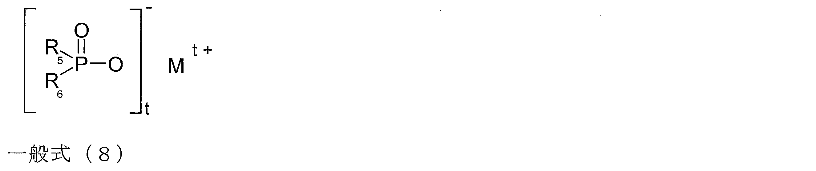
- the phosphinate is a compound represented by the following general formula (8).
- R 5 and R 6 each independently represent a linear or branched alkyl group or aryl group having 1 to 6 carbon atoms
- M represents Mg, Ca, Al, Sb, Sn, Ge, Ti , Fe, Zr, Zn, Ce, Bi, Sr, Mn, Li, Na
- K represents a metal selected from the group consisting of metals
- t is an integer of 1 to 4.
- the phosphinic acid salt is not particularly limited as long as it has the above structure.
- aluminum trisdiethylphosphinate, aluminum trismethylethylphosphinate, aluminum trisdiphenylphosphinate, zinc bisdiethylphosphinate, zinc bismethylethylphosphinate , Zinc bisdiphenylphosphinate, titanyl bisdiethylphosphinate, titanyl bismethylethylphosphinate, titanyl bisdiphenylphosphinate, and the like can be used alone or in combination of two or more.
- aluminum trisdiethylphosphinate and aluminum trismethylethylphosphinate containing a phosphorus element and an aluminum element are particularly preferred in that high flame retardancy is obtained.
- Examples of the fine particles containing aluminum element include gibbsite type aluminum hydroxide, boehmite type aluminum hydroxide, aluminum trisdiethylphosphinate, aluminum trismethylethylphosphinate, aluminum trisdiphenylphosphinate, and these can be used alone or Two or more types can be used in combination.
- examples of the fine particles containing magnesium element include magnesium hydroxide and magnesium oxide, and these can be used alone or in combination of two or more.
- the content of the component (c) of the present invention is preferably 20 to 80 parts by weight, more preferably 25 to 75 parts by weight with respect to 100 parts by weight of the component (a). Excellent in electrical insulation reliability.
- the amount of the component (c) is less than 20 parts by weight, the flame retardancy may be inferior.
- the amount is more than 80 parts by weight, the coating property when the resin composition is applied deteriorates, and the coating film at the time of coating Appearance defects may occur due to foaming or insufficient leveling.
- thermosetting resin of the present invention is one of the elements constituting the resin composition of the (B) insulating film, and is a compound that forms a crosslinked structure by heating and functions as a thermosetting agent.
- the insulating film is preferably obtained from a resin composition containing (d) a thermosetting resin.
- thermosetting resins include thermosetting resins such as epoxy resins, bismaleimide resins, bisallyl nadiimide resins, acrylic resins, methacrylic resins, hydrosilyl cured resins, allyl cured resins, and unsaturated polyester resins;
- a side chain reactive group type thermosetting polymer having a reactive group such as an allyl group, a vinyl group, an alkoxysilyl group, a hydrosilyl group, or the like at the side chain or the terminal of the polymer chain can be used. What is necessary is just to use combining the said thermosetting component 1 type (s) or 2 or more types as appropriate. Among these, it is more preferable to use an epoxy resin as the component (d).
- the epoxy resin is a compound containing at least one epoxy group in the molecule.
- a bisphenol A type epoxy resin product names jER828, jER1001, jER1002, and ADEKA manufactured by Japan Epoxy Resin Co., Ltd.
- Adeka Resin EP-4100E Adeka Resin EP-4300E
- trade names RE-310S and RE-410S manufactured by Nippon Kayaku Co., Ltd.
- the product names Epototo YD-115, Epototo YD-127, Epototo YD-128, manufactured by Toto Kasei Co., Ltd., and bisphenol F type epoxy resins are the product names jER806 and jER8 manufactured by Japan Epoxy Resins Co., Ltd. 7.
- Epiklon EXA-1514, hydrogenated bisphenol A type epoxy resin include trade names jERYX8000, jERYX8034, jERYL7170, and trade name Adeka Resin EP-408, manufactured by ADEKA Corporation.
- E DIC Corporation trade name Epicron EXA-7015, Toto Kasei Co., Ltd. trade name Epototo YD-3000, Epototo YD-4000D, and biphenyl type epoxy resin include trade names jERYX4000, Japan Epoxy Resin Co., Ltd. jERYL6121H, jERYL6640, jERYL6667, Nippon Kayaku Co., Ltd.
- trade names NC-3000, NC-3000H, phenoxy type epoxy resins, Japan Epoxy Resin Co., Ltd. trade names jER1256, jER4250, jER4275, naphthalene type epoxy resins Are the product names Epicron HP-4032, Epicron HP-4700, Epicron HP-4200, and Nippon Kayaku Co., Ltd.
- trade names jER152 and jER154 manufactured by Japan Epoxy Resin Co., Ltd. trade names EPPN-201-L manufactured by Nippon Kayaku Co., Ltd., trade names Epicron N-740 and Epicron N- manufactured by DIC Corporation.
- Etoto YDPN-638 trade name manufactured by Tohto Kasei Co., Ltd.
- cresol novolac type epoxy resins include trade names EOCN-1020, EOCN-102S, EOCN-103S, EOCN-104S, DIC shares manufactured by Nippon Kayaku Co., Ltd.
- the product names Epicron N-660, Epicron N-670, Epicron N-680, Epicron N-695, and trisphenolmethane type epoxy resins manufactured by the company are trade names EPPN-501H and EPPN-501HY manufactured by Nippon Kayaku Co., Ltd.
- EPPN-502H As the cyclopentadiene type epoxy resin, trade name XD-1000 manufactured by Nippon Kayaku Co., Ltd., the product name Epicron HP-7200 manufactured by DIC Co., Ltd., and as the amine type epoxy resin, trade name Epototo YH- by Toto Kasei Co., Ltd. 434, Epototo YH-434L, and flexible epoxy resins include trade names jER871, jER872, jERYL7175, jERYL7217, and trade names Epicron EXA-4850, manufactured by DIC Corporation, and urethane-modified epoxy resins.
- Adeka Resin EPU-6, Adeka Resin EPU-73, Adeka Resin EPU-78-11 manufactured by ADEKA Co., Ltd., and rubber-modified epoxy resins include Adeka Resin EPR-4023 manufactured by ADEKA Co., Ltd. Resin EPR-4026, Adeka Resin EPR-1309, as a chelate-modified epoxy resin, ADEKA Corporation under the trade name Adeka Resin EP-49-10, and the like Adecaresin EP-49-20.
- the component (d) according to the present invention is preferably 0.5 to 100 parts by weight, more preferably 1 part per 100 parts by weight of the sum of the components (a), (b), and (c). It is preferable that the amount is from 50 parts by weight, particularly preferably from 5 to 20 parts by weight, because the heat resistance, chemical resistance and electrical insulation reliability of the (B) insulating film can be improved.
- the heat resistance and electrical insulation reliability of the insulating film may be inferior.
- the (B) insulating film becomes brittle and poor in flexibility, and (B) the warping of the insulating film may be increased.
- the (e) photopolymerization initiator of the present invention is one of the elements constituting the resin composition of the (B) insulating film, and is activated by energy such as UV to initiate the reaction of the radical polymerizable group-containing resin. -It is a compound to promote. Therefore, the resin composition containing the (e) photopolymerization initiator of the present invention is a photosensitive resin composition.
- the insulating film is preferably obtained from a photosensitive resin composition containing (e) a photopolymerization initiator.
- component (e) of the present invention examples include Mihilaz ketone, 4,4′-bis (diethylamino) benzophenone, 4,4 ′, 4 ′′ -tris (dimethylamino) triphenylmethane, and 2,2′-.
- the (e) photopolymerization initiator according to the present invention is 0.1 to 50 parts by weight with respect to 100 parts by weight in total of the components (a), (b), (c), and (d). It is preferable that they are blended as described above. Since the photosensitivity of a resin composition improves by making it the said mixture ratio, it is preferable.
- the amount of the component (e) is less than the above range, the reaction of the radical polymerizable group at the time of light irradiation hardly occurs and the curing is often insufficient.
- adjustment of light irradiation amount becomes difficult and may be in an overexposure state. Therefore, in order to advance the photocuring reaction efficiently, it is preferable to adjust within the above range.
- additives such as a radical polymerizable resin, a colorant, an adhesion imparting agent, a polymerization inhibitor, and a solvent can be used as necessary.
- the radical polymerizable resin according to the present invention is not limited as long as (e) a resin in which a chemical bond is formed by a photopolymerization initiator. Furthermore, the radical polymerizable group is preferably a (meth) acryloyl group or a vinyl group.
- the radical polymerizable resin of the present invention is not particularly limited.
- the number of repeating units of EO (ethylene oxide) contained in one molecule of diacrylate or methacrylate is preferably 2 to 50, and more preferably 2 to 40.
- the solubility of the photosensitive resin composition in an aqueous developer typified by an alkaline aqueous solution is improved, and the development time is shortened.
- the EO-modified diacrylate or dimethacrylate together with an acrylic resin having 3 or more acrylic groups or methacrylic groups in order to improve developability.
- ethoxylated isocyanuric acid EO-modified triacrylate Ethoxylated isocyanuric acid EO modified trimethacrylate, ethoxylated trimethylolpropane triacrylate, ethoxylated trimethylolpropane triacrylate, ethoxylated trimethylolpropane triacrylate, trimethylolpropane triacrylate, propoxylated trimethylolpropane triacrylate, pentaerythritol tri Acrylate, ethoxylated pentaerythritol tetraacrylate, ethoxylated pentaerythritol tetraacrylate, ditrime Roll propane tetraacrylate, ditrimethylol propane tetraacrylate, propoxy
- hydroxyl groups in the molecular structure skeleton such as 2-hydroxy-3-phenoxypropyl acrylate, monohydroxyethyl acrylate phthalate, ⁇ -carboxy-polycaprolactone monoacrylate, acrylic acid dimer, pentaerythritol tri and tetraacrylate, Those having a carbonyl group are also preferably used.
- any radical polymerizable resin such as an epoxy-modified acrylic resin, a urethane-modified acrylic resin, or a polyester-modified acrylic resin may be used.
- the radical polymerizable resin in the present invention is 10 to 200 parts by weight with respect to a total of 100 parts by weight of the components (a), (b), (c), (d), and (e). It is preferable from the viewpoint that the photosensitivity of the photosensitive resin composition is improved.
- the amount of the radical polymerizable resin is less than the above range, the alkali resistance of the insulating film is lowered, and contrast may not be easily obtained when exposed and developed.
- productivity decreases because the stickiness of the coating film obtained by applying the photosensitive resin composition on the substrate and drying the solvent increases.
- the crosslinking density becomes too high, the insulating film may be brittle and easily cracked.
- Examples of the colorant of the present invention include phthalocyanine compounds, azo compounds, carbon black, and titanium oxide.
- Examples of the adhesion imparting agent include silane coupling agents, triazole compounds, tetrazole compounds, and triazine compounds.
- examples of the polymerization inhibitor include hydroquinone and hydroquinone monomethyl ether. These additives can be used alone or in combination of two or more.
- the solvent in the present invention is not particularly limited as long as it can dissolve the components (a) and (d).
- sulfoxide solvents such as dimethyl sulfoxide and diethyl sulfoxide, methyl monoglyme (1, 1, 2-dimethoxyethane), methyldiglyme (bis (2-methoxyether) ether), methyltriglyme (1,2-bis (2-methoxyethoxy) ethane), methyltetraglyme (bis [2- (2-methoxy) Ethoxyethyl)] ether), ethylmonoglyme (1,2-diethoxyethane), ethyldiglyme (bis (2-ethoxyethyl) ether), butyldiglyme (bis (2-butoxyethyl) ether), etc.
- Glycol diethers ⁇ -butyrolactone, methyl acetate, ethyl acetate, isopropyl N-propyl acetate, butyl acetate, propylene glycol monomethyl ether acetate, ethylene glycol monobutyl ether acetate, diethylene glycol monoethyl ether acetate (also known as carbitol acetate, 2- (2-butoxyethoxy) ethyl acetate)), diethylene glycol mono Acetates such as butyl ether acetate, 3-methoxybutyl acetate, ethylene glycol monomethyl ether acetate, ethylene glycol monoethyl ether acetate, dipropylene glycol methyl ether acetate, propylene glycol diacetate, 1,3-butylene glycol diacetate, and dipropylene Glycol methyl ether, tripropylene glycol methyl ether Propylene glycol n-propyl ether, diprop
- a preferable blending amount of the solvent of the present invention is 10 to 400 parts by weight with respect to 100 parts by weight of the total of the components (a), (b), (c), (d), and (e). More preferred is 20 to 200 parts by weight, and particularly preferred is 40 to 100 parts by weight.
- the amount of the solvent within the above range because the viscosity and viscosity of the resin composition can be adjusted within a range suitable for coating such as screen printing.
- the viscosity of the resin composition becomes very high, coating becomes difficult, and foam entrainment during coating may be inferior in leveling properties.
- the viscosity of a resin composition will become very low, application
- coating will become difficult and the circuit coverage may be inferior.
- Insulating film of the present invention is a resin composition in which each component (a), component (b), component (c), component (d), component (e), and other components are uniformly mixed. After the product is obtained, this resin composition can be obtained by forming a fine opening on the film with a wiring pattern (C) by exposure / development and performing heat treatment as necessary.
- the method of uniformly mixing is not particularly limited, but may be mixed by using a general kneading apparatus such as a three roll or bead mill apparatus. Moreover, when the viscosity of a solution is low, you may mix using a general stirring apparatus. Among these, it is preferable to mix and pulverize and disperse using three rolls because the component (c) has a uniform size.
- the particle diameter of each component in the resin composition after mixing can be measured by a method using a gauge specified in JIS K 5600-2-5. Moreover, if a particle size distribution measuring apparatus is used, an average particle diameter, a particle diameter, and a particle size distribution can be measured.
- an insulating film can be obtained by an arbitrary method.
- the resin composition is applied as it is to the (C) film with a wiring pattern and cured to form.
- Application to the film with the wiring pattern can be performed by screen printing, roller coating, curtain coating, spray coating, spin coating using a spinner, or the like.
- the coating film (preferably thickness: 5 to 100 ⁇ m) is dried at 120 ° C. or lower, preferably 40 to 100 ° C.
- a negative photomask is placed on the dried coating film, and exposure is performed by irradiating active rays such as ultraviolet rays, visible rays, and electron beams.
- active rays such as ultraviolet rays, visible rays, and electron beams.
- the fine opening can be obtained by developing the unexposed portion with a developer using various methods such as shower, paddle, immersion, or ultrasonic wave. Since the time until the pattern is exposed varies depending on the spraying pressure and flow rate of the developing device and the temperature of the etching solution, it is desirable to find the optimum device conditions as appropriate.
- This developer may contain a water-soluble organic solvent such as methanol, ethanol, n-propanol, isopropanol, or N-methyl-2-pyrrolidone.
- alkaline compound that gives the alkaline aqueous solution include hydroxides, carbonates, hydrogen carbonates, amine compounds, and the like of alkali metals, alkaline earth metals, or ammonium ions, and specifically sodium hydroxide.
- Ropiruamin aqueous solution with compounds of other long as it exhibits basicity can also be naturally used.
- the temperature of the developer depends on the composition of the resin composition and the composition of the alkaline developer, and is generally 0 ° C. or higher and 80 ° C. or lower, more generally 10 ° C. or higher and 60 ° C. or lower. It is preferable to do.
- the fine openings formed by the development process are rinsed to remove unnecessary residues.
- the rinsing liquid include water and acidic aqueous solutions.
- the thickness of the (B) cured film is determined in consideration of (C) the thickness of the film with a wiring pattern, etc., but is preferably about 2 to 50 ⁇ m.
- the final heat treatment temperature at this time is preferably 100 ° C. or more and 250 ° C. or less, and more preferably 120 for the purpose of preventing oxidation of the conductor circuit and the like and (C) not lowering the adhesion with the film with the wiring pattern. It is 130 degreeC or more and 180 degrees C or less especially preferably.
- the temperature at which the solvent is removed by performing the above heating and / or hot air blowing may be such that the thermosetting resin or the like contained in the resin composition does not undergo a crosslinking reaction by heating.
- the support to be used is not particularly limited, but various commercially available films such as a polyethylene terephthalate (PET) film, a polyphenylene sulfide film, and a polyimide film can be used.
- PET polyethylene terephthalate
- a PET film is often used because it has a certain degree of heat resistance and is relatively inexpensive.
- the protective film is preferably laminated and laminated on the surface of the resin composition at a temperature of 10 ° C. to 50 ° C.
- the temperature at the time of lamination processing becomes higher than 50 degreeC, the thermal expansion of a protective film will be caused and the wrinkle and curl of the protective film after a lamination process may arise.
- a protective film peels at the time of use, it is desirable for the joint surface of a protective film and a resin composition to have appropriate adhesiveness at the time of storage, and to be excellent in peelability.
- the material of the protective film is not particularly limited.
- a polyethylene film (PE film), a polyethylene vinyl alcohol film (EVA film), a “copolymer film of polyethylene and ethylene vinyl alcohol” hereinafter referred to as ( "PE + EVA) copolymer film”, “PE film and (PE + EVA) copolymer film laminate”, or "(PE + EVA) copolymer and polyethylene film by simultaneous extrusion process” (Film having one surface being a PE film surface and the other surface being a (PE + EVA) copolymer film surface).
- thermocompression bonding may be performed by hot pressing, laminating (thermal laminating), hot roll laminating or the like, and is not particularly limited.
- the processing temperature may be equal to or higher than a lower limit temperature at which the laminating process can be performed (hereinafter, a pressure bonding possible temperature).
- the pressure-bondable temperature is preferably in the range of 50 to 150 ° C., more preferably in the range of 60 to 120 ° C., and particularly preferably in the range of 80 ° C. to 120 ° C. If the treatment temperature exceeds 150 ° C., a crosslinking reaction due to heating of the resin composition may occur during the lamination treatment, and curing of the resin composition may proceed. On the other hand, when the processing temperature is less than 50 ° C., the fluidity of the resin composition is low, and it becomes difficult to embed the pattern circuit.
- the filmed resin composition is kept in an uncured state. Therefore, when thermocompression treatment such as thermal laminating treatment is performed, it has appropriate fluidity and can be suitably embedded in a conductor circuit of a film with a wiring pattern.
- the bonded sample in which the resin composition is laminated on the film with the wiring pattern and the support is further laminated is obtained by the above-described thermocompression treatment.
- a negative photomask is placed on the support of the bonded sample, and exposure is performed by irradiating active light such as ultraviolet light, visible light, or electron beam.
- active light such as ultraviolet light, visible light, or electron beam.
- the support is peeled off, and a fine opening can be obtained by developing the unexposed portion with a developer using various methods such as shower, paddle, immersion, or ultrasonic wave. Since the time until the pattern is exposed varies depending on the spraying pressure and flow rate of the developing device and the temperature of the etching solution, it is desirable to find the optimum device conditions as appropriate.
- This developer may contain a water-soluble organic solvent such as methanol, ethanol, n-propanol, isopropanol, or N-methyl-2-pyrrolidone.
- alkaline compound that gives the alkaline aqueous solution include hydroxides, carbonates, hydrogen carbonates, amine compounds, and the like of alkali metals, alkaline earth metals, or ammonium ions, and specifically sodium hydroxide.
- Ropiruamin aqueous solution with compounds of other long as it exhibits basicity can also be naturally used.
- the temperature of the developer depends on the composition of the resin composition and the composition of the alkaline developer, and is generally 0 ° C. or higher and 80 ° C. or lower, more generally 10 ° C. or higher and 60 ° C. or lower. It is preferable to do.
- the fine openings formed by the development process are rinsed to remove unnecessary residues.
- the rinsing liquid include water and acidic aqueous solutions.
- the thickness of the insulating film is determined in consideration of (C) the thickness of the film with a wiring pattern, etc., but is preferably about 2 to 50 ⁇ m.
- the final heat treatment temperature at this time is preferably 100 ° C. or more and 250 ° C. or less, and more preferably 120 for the purpose of preventing oxidation of the conductor circuit and the like and (C) not lowering the adhesion with the film with the wiring pattern. It is 130 degreeC or more and 180 degrees C or less especially preferably.
- the film with a wiring pattern of the present invention is a film having a wiring pattern on one side or both sides of a base film having a thickness of 5 to 100 ⁇ m.
- the production method of the film with a wiring pattern in the present invention is not particularly limited.
- a flexible metal-clad laminate is produced by forming a conductor layer on the base film, and the conductor layer is produced by pattern etching. Can do.
- the base film in the present invention is not particularly limited as long as it is flexible and has an insulating property.
- polyimide film is preferable.
- the conductor layer in the present invention is not particularly limited, and examples thereof include copper or copper alloy, stainless steel or its alloy, nickel or nickel alloy (including 42 alloy), aluminum or aluminum alloy.
- copper foil such as rolled copper foil and electrolytic copper foil is frequently used, but it can also be preferably used in the present invention.
- the antirust layer, the heat-resistant layer, or the contact bonding layer may be apply
- a method for forming a conductor layer on the base film in the present invention that is, a method for producing a flexible metal-clad laminate is not particularly limited, and examples thereof include a casting method, a laminating method, and a metalizing method.
- the casting method is a method in which a liquid base film solution is applied onto a conductor layer, dried and thermally cured
- the laminating method is a method in which the base film and the conductor layer are formed by thermocompression bonding.
- the laminate method includes a so-called three-layer metal-clad laminate and a so-called two-layer metal-clad laminate when the adhesive is not formed between the base film and the conductor layer.
- the adhesive include an epoxy resin and an acrylic resin.
- the metalizing method is a method in which a metal thin film is formed on a base film by a vacuum deposition method or a sputtering method, and a conductor layer is formed by wet plating.
- the conductor layer may be formed by wet plating without forming a metal thin film.
- the conductor layer can be formed on one side or both sides of the base film.
- a pattern etching method of the conductor layer in this invention For example, the photoresist method is mentioned.
- the photoresist method is a method in which a photoresist layer is formed on a metal-clad laminate, and a wiring pattern is formed by exposure, development, etching of a conductor layer, and peeling of a dry film.
- a negative type or a positive type can be used, and a liquid form, a film form, or the like can be used.
- the photoresist is not particularly limited, and examples thereof include a method of forming a negative dry film type resist on a metal-clad laminate by thermal lamination or applying and drying a positive liquid type resist. .
- the portions other than the exposed portion are removed by development, while in the case of the positive type, the exposed portion is removed by development.
- a dry film type resist can be easily thickened.
- the negative dry film type photoresist examples include trade name SPG-152 manufactured by Asahi Kasei Corporation and trade name RY-3215 manufactured by Hitachi Chemical Co., Ltd.
- a known agent for removing the photoresist layer can be appropriately selected and used.
- an aqueous sodium carbonate solution (0.2 to 1.5%, etc.) can be sprayed.
- the photoresist layer can be developed and removed.
- known conductor layer etching can be appropriately selected and used.
- potassium ferricyanide aqueous solution iron chloride aqueous solution, copper chloride aqueous solution, ammonium persulfate aqueous solution, sodium persulfate aqueous solution, hydrogen peroxide solution , Hydrofluoric acid aqueous solutions, and combinations thereof can be used.
- the conductive layer-integrated FPC of the present invention has excellent adhesion between the conductive layer having an electromagnetic wave shielding function and the insulating film, and is excellent in flexibility, flame retardancy, electrical insulation reliability, and small warpage. Therefore, it is particularly suitable as a liquid crystal display, a sensor, and an FPC for a camera module of a small portable terminal. Further, it is also used for hinge bending, slide bending, cable, connector, FPC for optical pickup of hard disk, and the like.
- the poly (meth) acrylic resin solution obtained had a solid content concentration of 48%, a weight average molecular weight of 48,000, and an acid value of 78 mgKOH / g.
- the solid content concentration, weight average molecular weight, and acid value were measured by the following methods.
- a trade name SF-PC5500 of Tatsuta Electric Wire Co., Ltd. which is a film type conductive layer, is 150 ° C., 2.5 MPa, 60 minutes. Were bonded together by a hot press to prepare a conductive layer integrated FPC evaluation test piece.
- a trade name SF-PC5500 of Tatsuta Electric Wire Co., Ltd. which is a film type conductive layer, is 150 ° C., 2.5 MPa, 60 minutes.
- a hot press were bonded together by a hot press to prepare a conductive layer integrated FPC evaluation test piece.
- the obtained test piece was cut into a 30 mm ⁇ 10 mm strip, bent at 180 ° by 10 times and bent, and the coating film was visually confirmed to check for cracks.
- Warping Test piece obtained by the same method as in (iii) Flexibility item was cut into an area of 50 mm ⁇ 50 mm and placed on a smooth table so that the conductive layer surface was the upper surface, and the warp height at the end of the test piece was measured. A schematic diagram of the measurement site is shown in FIG. The smaller the amount of warpage, the lower the amount of warpage when the conductor layer integrated FPC is used. The warp amount is preferably 5 mm or less.
- (V) Flame retardancy In accordance with the flame retardancy test standard UL94 for plastic materials, the flame retardancy test was performed as follows. A cured film laminated film of the resin composition was prepared on one side of a polyimide film having a thickness of 25 ⁇ m (Apical 25NPI manufactured by Kaneka Corporation) in the same manner as in the above item ⁇ Preparation of conductive layer-integrated FPC evaluation test piece>. Further, on the insulating film of the obtained resin composition, as a conductive layer having an electromagnetic wave shielding function, a trade name SF-PC5500 of Tatsuta Electric Wire Co., Ltd., which is a film type conductive layer, is 150 ° C., 2.5 MPa, 60 minutes.
- test piece was cut into dimensions: 50 mm width ⁇ 200 mm length, marked with a 125 mm portion, rounded into a cylinder with a diameter of about 13 mm, and an overlapped portion (75 mm location) above the marked line, And PI tape was stuck so that there might be no gap in the upper part, and 20 tubes for a flame retardant test were prepared.
- 10 were treated at (1) 23 ° C./50% relative humidity / 48 hours, and the remaining 10 were treated at (2) 70 ° C. for 168 hours and then cooled in a desiccator containing anhydrous calcium chloride for 4 hours or more.
- an insulating film of a resin composition having a thickness of 20 ⁇ m was produced on the film with a wiring pattern by the same method as described above in ⁇ Production of conductive layer integrated FPC evaluation test piece>.
- a trade name SF-PC5500 of Tatsuta Electric Wire Co., Ltd. which is a film type conductive layer, is 150 ° C., 2.5 MPa, 60 minutes.
- a hot press was used to prepare a conductive layer integrated FPC evaluation test piece.
- a DC current of 20 V was applied to both terminal portions of the test piece in an environmental test machine at 40 ° C.
- ⁇ A resistance value of 10 8 or more in 1000 hours after the start of the test, and no occurrence of migration or dendrite.
- X Migration, dendrite, etc. occurred in 1000 hours after the start of the test.
- a trade name SF-PC5500 of Tatsuta Electric Wire Co., Ltd. which is a film type conductive layer, is 150 ° C., 2.5 MPa, 60 minutes. Were bonded together by a hot press to prepare a conductive layer integrated FPC evaluation test piece.
- a trade name SF-PC5500 of Tatsuta Electric Wire Co., Ltd. which is a film type conductive layer, is 150 ° C., 2.5 MPa, 60 minutes.
- a hot press were bonded together by a hot press to prepare a conductive layer integrated FPC evaluation test piece.
- the obtained test piece was cut into a 30 mm ⁇ 10 mm strip, bent at 180 ° by 10 times and bent, and the coating film was visually confirmed to check for cracks.
- Warping Test piece obtained by the same method as in (iii) Flexibility item was cut into an area of 50 mm ⁇ 50 mm and placed on a smooth table so that the conductive layer surface was the upper surface, and the warp height at the end of the test piece was measured. A schematic diagram of the measurement site is shown in FIG. The smaller the amount of warpage, the lower the amount of warpage when the conductor layer integrated FPC is used. The warp amount is preferably 5 mm or less.
- test piece was cut into dimensions: 50 mm width ⁇ 200 mm length, marked with a 125 mm portion, rounded into a cylinder with a diameter of about 13 mm, and an overlapped portion (75 mm location) above the marked line, And PI tape was stuck so that there might be no gap in the upper part, and 20 tubes for a flame retardant test were prepared.
- 10 were treated at (1) 23 ° C./50% relative humidity / 48 hours, and the remaining 10 were treated at (2) 70 ° C. for 168 hours and then cooled in a desiccator containing anhydrous calcium chloride for 4 hours or more.
- an insulating film of a photosensitive resin composition having a thickness of 20 ⁇ m is formed on the single-sided wiring pattern on the film with the wiring pattern by the same method as in the above item ⁇ Preparation of conductive layer-integrated FPC evaluation test piece>.
- a trade name SF-PC5500 of Tatsuta Electric Wire Co., Ltd. which is a film type conductive layer, is heated at 150 ° C., 2.5 MPa, 60 minutes.
- the conductive layer integrated type FPC evaluation test piece was produced by laminating with a press.
- a DC current of 20 V was applied to both terminal portions of the test piece in an environmental test machine at 40 ° C. and 90% RH, and changes in insulation resistance value, occurrence of migration, etc. were observed.
- ⁇ A resistance value of 10 8 or more in 1000 hours after the start of the test, and no occurrence of migration or dendrite.
- X Migration, dendrite, etc. occurred in 1000 hours after the start of the test.
- the present invention is used for electromagnetic wave noise countermeasures in electronic devices such as mobile phones, video cameras, and notebook computers.
Landscapes
- Engineering & Computer Science (AREA)
- Microelectronics & Electronic Packaging (AREA)
- Physics & Mathematics (AREA)
- Electromagnetism (AREA)
- Manufacturing & Machinery (AREA)
- Laminated Bodies (AREA)
- Non-Metallic Protective Coatings For Printed Circuits (AREA)
- Structure Of Printed Boards (AREA)
- Shielding Devices Or Components To Electric Or Magnetic Fields (AREA)
Abstract
Description
本願発明の導電層一体型FPCの構成図を図1に示すが、これに限定されるものではない。先ず、配線パターン(2)およびベースフィルム(3)からなる(C)配線パターン付きフィルム(1)上に(B)絶縁膜(4)を形成し、FPC(5)を得る。続いて、(A)電磁波シールド機能を有する導電層(6)を(B)絶縁膜(4)上に形成する事で本願発明の導電層一体型FPCを得ることができる。
本願発明における(A)電磁波シールド機能を有する導電層とは、10dB以上の電磁波遮断効果を示し、導電性を示す層である。一般的に、導電層の導電率が高いほど、電磁波シールド効果が高い。従って、導電率の高い金属、例えば、(f)銀、銅、アルミニウム及びニッケルからなる群から選ばれる少なくとも1種の元素を含有していることがより好ましい。
シールド材が無い場合の空間の電界強度:Eo
シールド材が有る場合の空間の電界強度:Ex
本願発明における(A)電磁波シールド機能を有する導電層は、特に限定されないが、例えば、(A-1)フィルムタイプ、(A-2)ペーストタイプ、又は(A-3)金属薄膜タイプなどが挙げられ、特に、フィルムタイプは導電層一体型FPCの柔軟性を損なうことなく、シールド特性を付与できるため好ましい。
本願発明におけるフィルムタイプの電磁波シールド機能を有する導電層は、特に限定されないが、例えば、導電性粒子を樹脂に分散させたフィルムとしては、トウヨウケム株式会社社製の商品名TSS100-18、TSS100-22等が挙げられる。また、導電性接着剤/金属薄膜/絶縁層のように多層化した多層フィルムとしては、タツタ電線株式会社の商品名SF-PC5000、SF-PC5100、SF-PC5500、SF-PC5600、SF-PC5900、SF-PC6000等が挙げられる。
本願発明におけるペーストタイプの電磁波シールド機能を有する導電層は、特に限定されないが、例えば、銀粒子を樹脂に分散させたペーストとしては、トウヨウケム株式会社製の商品名RA FS039、藤倉化成株式会社製の商品名XA-9015が挙げられる。また、ニッケル粒子を樹脂に分散させたペーストとしては、藤倉化成株式会社製の商品名FN-101、ペルノックス株式会社製の商品名K-3435G等が挙げられる。
(A-3)金属薄膜タイプ
本願発明における金属薄膜タイプの電磁波シールド機能を有する導電層とは、絶縁膜上に直接金属薄膜を形成する事により得られる導電層である。本願発明における金属薄膜タイプの電磁波シールド機能を有する導電層を絶縁膜上に形成する方法は、特に限定されないが、例えば、真空蒸着法、スパッタリング法、イオンプレーティング法等の物理的気相成長法(PVD)、化学的気相成長法(CVD)又は、無電解めっき等の液相成長法が挙げられる。特に、量産性を考慮すれば真空蒸着が望ましく、安価で安定した金属薄膜を得ることができるため好ましい。本願発明における真空蒸着法とは、真空条件下で金属を加熱し、気化あるいは昇華させ、目的となる基材表面に金属薄膜を形成する方法である。蒸着金属としては、特に限定されないが、例えば、銀、銅、アルミニウム、金等が挙げられる。
本願発明における(B)絶縁膜とは、絶縁性を有する厚さ5~100μmの膜である。
本願発明における(a)バインダーポリマーとは、有機溶媒に対して可溶性であり、重量平均分子量が、ポリエチレングリコール換算で1,000以上、1,000,000以下のポリマーである。
使用装置:東ソーHLC-8220GPC相当品
カラム :東ソー TSK gel Super AWM-H(6.0mmI.D.×15cm)×2本
ガードカラム:東ソー TSK guard column Super AW-H
溶離液:30mM LiBr+20mM H3PO4 in DMF
流速:0.6mL/min
カラム温度:40℃
検出条件:RI:ポラリティ(+)、レスポンス(0.5sec)
試料濃度:約5mg/mL
標準品:PEG(ポリエチレングリコール)
上記範囲内に重量平均分子量を制御することにより、得られる(B)絶縁膜の柔軟性、耐薬品性が優れるため好ましい。重量平均分子量が1,000以下の場合は、(B)絶縁膜の柔軟性や耐薬品性が低下する場合があり、重量平均分子量が1,000,000以上の場合は(a)成分及び(b)成分を含む樹脂組成物の粘度が高くなる場合がある。

で示されるジオール化合物と、下記一般式(2)

で示されるジイソシアネート化合物を反応させることにより、下記一般式(3)
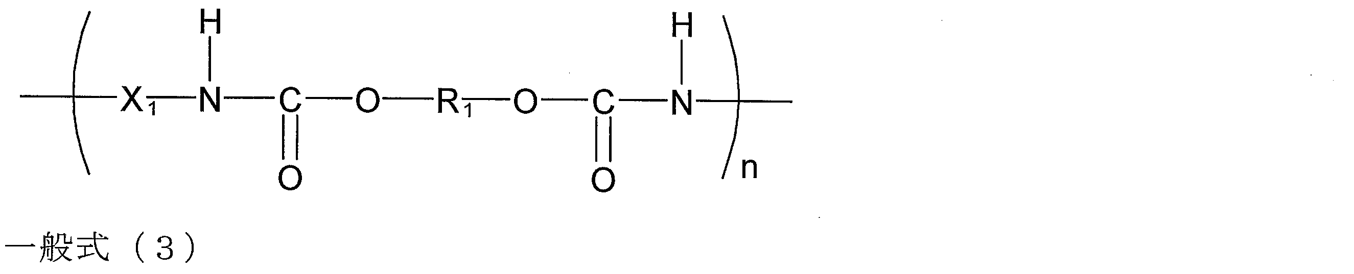

で示される水酸基及び少なくとも1つの(メタ)アクリロイル基を含有する化合物及び/又は下記一般式(5)

で示されるイソシアネート基及び少なくとも1つの(メタ)アクリロイル基を含有する化合物を反応させることにより得られる。

で示される2つの水酸基及び1つのカルボキシル基を含有する化合物を反応させることにより得られる。

で示されるテトラカルボン酸二無水物を反応させることにより得られる。
本願発明における(b)球状有機ビーズとは、炭素を含む球状ポリマーで、楕円状のものも含まれる。
装置:株式会社堀場製作所製 LA-950V2相当品
測定方式:レーザー回折/散乱式。
導電層一体型FPCにおいて、5mm×3mmの範囲をカッターナイフで切り出し、エポキシ系包埋樹脂及びカバーガラスを使用して切り出した導電層一体型FPCの両面に保護膜層及びカバーガラス層を形成した後、絶縁膜の厚み方向の断面をイオンビームによるクロスセクションポリッシャ加工を行った。
使用装置:日本電子株式会社製 SM-09020CP相当品
加工条件:加速電圧 6kV
(絶縁膜の断面観察)
上記得られた絶縁膜の厚み方向の断面について、走査型電子顕微鏡により観察を行った。
使用装置:株式会社日立ハイテクノロジーズ製 S-3000N相当品
観察条件:加速電圧 15kV
検出器:反射電子検出(組成モード)
倍率:1000倍。
本願発明の(c)リン、アルミニウム及びマグネシウムからなる群から選ばれる少なくとも1種の元素を含有する微粒子とは、構造中に少なくとも1つのリン、アルミニウム及びマグネシウムからなる群から選ばれる少なくとも1種の元素を有している微粒子である。
使用装置:株式会社堀場製作所製 EMAX-7000相当品
分析条件:加速電圧 15kV 積算時間900秒。
上記ホスフィン酸塩は、上記構造であれば特に限定はされないが、例えば、トリスジエチルホスフィン酸アルミニウム、トリスメチルエチルホスフィン酸アルミニウム、トリスジフェニルホスフィン酸アルミニウム、ビスジエチルホスフィン酸亜鉛、ビスメチルエチルホスフィン酸亜鉛、ビスジフェニルホスフィン酸亜鉛、ビスジエチルホスフィン酸チタニル、ビスメチルエチルホスフィン酸チタニル、ビスジフェニルホスフィン酸チタニル等を挙げることができ、これらは単独であるいは2種類以上を組み合わせて用いることができる。上記の中でも特に、リン元素及びアルミニウム元素を含有するトリスジエチルホスフィン酸アルミニウム、トリスメチルエチルホスフィン酸アルミニウムを用いた場合、高い難燃性が得られる点で好ましい。
本願発明の(d)熱硬化性樹脂は、(B)絶縁膜の樹脂組成物を構成する要素の一つであり、加熱により架橋構造を形成し、熱硬化剤として機能する化合物である。本発明においては、(B)絶縁膜が、(d)熱硬化性樹脂を含有している樹脂組成物から得られることが好ましい。(d)熱硬化性樹脂としては、例えば、エポキシ樹脂、ビスマレイミド樹脂、ビスアリルナジイミド樹脂、アクリル樹脂、メタクリル樹脂、ヒドロシリル硬化樹脂、アリル硬化樹脂、不飽和ポリエステル樹脂等の熱硬化性樹脂;高分子鎖の側鎖または末端にアリル基、ビニル基、アルコキシシリル基、ヒドロシリル基、等の反応性基を有する側鎖反応性基型熱硬化性高分子等を用いることができる。上記熱硬化性成分、1種又は2種以上を適宜組み合わせて用いればよい。(d)成分としては、この中でも、エポキシ樹脂を用いることがより好ましい。エポキシ樹脂成分を含有することにより、絶縁膜に対して耐熱性を付与できると共に、配線パターン付きフィルムに対する接着性、更には電磁波シールド材との密着性を付与することができるため好ましい。上記エポキシ樹脂とは、分子内に少なくとも1個のエポキシ基を含む化合物であり、例えば、ビスフェノールA型エポキシ樹脂としては、ジャパンエポキシレジン株式会社製の商品名jER828、jER1001、jER1002、株式会社ADEKA製の商品名アデカレジンEP-4100E、アデカレジンEP-4300E、日本化薬株式会社製の商品名RE-310S、RE-410S、大日本インキ株式会社製の商品名エピクロン840S、エピクロン850S、エピクロン1050、エピクロン7050、東都化成株式会社製の商品名エポトートYD-115、エポトートYD-127、エポトートYD-128、ビスフェノールF型エポキシ樹脂としては、ジャパンエポキシレジン株式会社製の商品名jER806、jER807、株式会社ADEKA製の商品名アデカレジンEP-4901E、アデカレジンEP-4930、アデカレジンEP-4950、日本化薬株式会社製の商品名RE-303S、RE-304S、RE-403S,RE-404S、DIC株式会社製の商品名エピクロン830、エピクロン835、東都化成株式会社製の商品名エポトートYDF-170、エポトートYDF-175S、エポトートYDF-2001、ビスフェノールS型エポキシ樹脂としては、DIC株式会社製の商品名エピクロンEXA-1514、水添ビスフェノールA型エポキシ樹脂としては、ジャパンエポキシレジン株式会社製の商品名jERYX8000、jERYX8034,jERYL7170、株式会社ADEKA製の商品名アデカレジンEP-4080E、DIC株式会社製の商品名エピクロンEXA-7015、東都化成株式会社製の商品名エポトートYD-3000、エポトートYD-4000D、ビフェニル型エポキシ樹脂としては、ジャパンエポキシレジン株式会社製の商品名jERYX4000、jERYL6121H、jERYL6640、jERYL6677、日本化薬株式会社製の商品名NC-3000、NC-3000H、フェノキシ型エポキシ樹脂としては、ジャパンエポキシレジン株式会社製の商品名jER1256、jER4250、jER4275、ナフタレン型エポキシ樹脂としては、DIC株式会社製の商品名エピクロンHP-4032、エピクロンHP-4700、エピクロンHP-4200、日本化薬株式会社製の商品名NC-7000L、フェノールノボラック型エポキシ樹脂としては、ジャパンエポキシレジン株式会社製の商品名jER152、jER154、日本化薬株式会社製の商品名EPPN-201-L、DIC株式会社製の商品名エピクロンN-740、エピクロンN-770、東都化成株式会社製の商品名エポトートYDPN-638、クレゾールノボラック型エポキシ樹脂としては、日本化薬株式会社製の商品名EOCN-1020、EOCN-102S、EOCN-103S、EOCN-104S、DIC株式会社製の商品名エピクロンN-660、エピクロンN-670、エピクロンN-680、エピクロンN-695、トリスフェノールメタン型エポキシ樹脂としては、日本化薬株式会社製の商品名EPPN-501H、EPPN-501HY、EPPN-502H、ジシクロペンタジエン型エポキシ樹脂としては、日本化薬株式会社製の商品名XD-1000、DIC株式会社製の商品名エピクロンHP-7200、アミン型エポキシ樹脂としては、東都化成株式会社の商品名エポトートYH-434、エポトートYH-434L、可とう性エポキシ樹脂としては、ジャパンエポキシレジン株式会社製の商品名jER871、jER872、jERYL7175、jERYL7217、DIC株式会社製の商品名エピクロンEXA-4850、ウレタン変性エポキシ樹脂としては、株式会社ADEKA製の商品名アデカレジンEPU-6、アデカレジンEPU-73、アデカレジンEPU-78-11、ゴム変性エポキシ樹脂としては、株式会社ADEKA製の商品名アデカレジンEPR-4023、アデカレジンEPR-4026、アデカレジンEPR-1309、キレート変性エポキシ樹脂としては、株式会社ADEKA製の商品名アデカレジンEP-49-10、アデカレジンEP-49-20等が挙げられる。
本願発明の(e)光重合開始剤とは、(B)絶縁膜の樹脂組成物を構成する要素の一つであり、UVなどのエネルギーによって活性化し、ラジカル重合性基含有樹脂の反応を開始・促進させる化合物である。したがって、本願発明の(e)光重合開始剤を含有する樹脂組成物は、感光性樹脂組成物となる。本願発明は、(B)絶縁膜が(e)光重合開始剤を含有している感光性樹脂組成物から得られることが好ましい。本願発明の(e)成分としては、例えば、ミヒラ-ズケトン、4,4’-ビス(ジエチルアミノ)ベンゾフェノン、4,4’,4’’-トリス(ジメチルアミノ)トリフェニルメタン、2,2’-ビス(2-クロロフェニル)-4,4’,5,5’-テトラフェニル-1,2’-ジイミダゾール、アセトフェノン、ベンゾイン、2-メチルベンゾイン、ベンゾインメチルエ-テル、ベンゾインエチルエ-テル、ベンゾインイソプロピルエ-テル、ベンゾインイソブチルエ-テル、2-t-ブチルアントラキノン、1,2-ベンゾ-9,10-アントラキノン、メチルアントラキノン、チオキサントン、2,4-ジエチルチオキサントン、2-イソプロピルチオキサントン、1-ヒドロキシシクロヘキシルフェニルケトン、ジアセチルベンジル、ベンジルジメチルケタ-ル、ベンジルジエチルケタ-ル、2(2’-フリルエチリデン)-4,6-ビス(トリクロロメチル)-S-トリアジン、2[2’(5’’-メチルフリル)エチリデン]-4,6-ビス(トリクロロメチル)-S-トリアジン、2(p-メトキシフェニル)-4,6-ビス(トリクロロメチル)-S-トリアジン、2,6-ジ(p-アジドベンザル)-4-メチルシクロヘキサノン、4,4’-ジアジドカルコン、ジ(テトラアルキルアンモニウム)-4,4’-ジアジドスチルベン-2,2’-ジスルフォネ-ト、2,2-ジメトキシ-1,2-ジフェニルエタン-1-オン、1-ヒドロキシ-シクロヘキシル-フェニル-ケトン、2-ヒドロキシ-2-メチル-1-フェニル-プロパン-1-オン、1-[4-(2-ヒドロキシエトキシ)-フェニル]-2-ヒドロキシ-2-メチル-1-プロパン-1-オン、2-メチル-1-[4-(メチルチオ)フェニル]-2-モルフォリノプロパン-1-オン、2-ベンジル-2-ジメチルアミノ-1-(4-モルフォリノフェニル)-ブタン-1、ビス(2,4,6-トリメチルベンゾイル)-フェニルフォスフィンオキサイド、ビス(2,6-ジメトキシベンゾイル)-2,4,4-トリメチル-ペンチルフォスフィンオキサイド、2,4,6-トリメチルベンゾイル-ジフェニル-フォスフィンオキサイド、2-ヒドロキシ-2-メチル-1-フェニル-プロパン-1-ケトン、ビス(n5-2,4-シクロペンタジエン-1-イル)-ビス(2,6-ジフルオロ-3-(1H-ピロール-1-イル)-フェニル)チタニウム、1,2-オクタンジオン,1-[4-(フェニルチオ)-,2-(O-ベンゾイルオキシム)]、ヨード二ウム,(4-メチルフェニル)[4-(2-メチルプロピル)フェニル]-ヘキサフルオロフォスフェート(1-)、エチル-4-ジメチルアミノベンゾエート、2-エチルヘキシル-4-ジメチルアミノベンゾエート、エタノン,1-[9-エチル-6-(2-メチルベンゾイル)-9H-カルバゾール-3-イル]-,1-(O-アセチルオキシオム)などが挙げられる。上記(e)光重合開始剤は適宜選択することが望ましく、1種以上を混合させて用いることが望ましい。
本願発明の(B)絶縁膜の樹脂組成物には、更に必要に応じて、ラジカル重合性樹脂、着色剤、密着性付与剤、重合禁止剤、溶媒等の添加剤を用いることができる。
本願発明の配線パターン付きフィルムとは、厚さ5~100μmのベースフィルムの片面又は両面に配線パターンを有するフィルムである。本願発明における配線パターン付きフィルムの作製方法は、特に限定されないが、例えば、ベースフィルムに導体層を形成することにより、フレキシブル金属張積層板を作製し、導体層をパターンエッチングする事によって作製することができる。
本願発明におけるベースフィルムは、柔軟性があり、かつ絶縁性を有するフィルムであれば特に限定されないが、例えば、ポリプロピレン、架橋ポリエチレン、ポリエステル、ポリベンズイミダゾール、ポリイミド、ポリイミドアミド、ポリエーテルイミド、ポリフェニレンサルファイド、液晶ポリマー、ポリエーテルエーテルケトンなどが挙げられ、耐熱性を要求されない場合は、安価なポリエステルフィルムが好ましく、耐熱性が要求される場合にはポリイミドフィルムが好ましい。
本願発明における導体層のパターンエッチング方法としては、特に限定されないが、例えば、フォトレジスト法が挙げられる。フォトレジスト法とは、フォトレジスト層を金属張積層板上に形成し、露光、現像、導体層のエッチング、ドライフィルムの剥離によって配線パターンを形成する方法である。フォトレジスト層としては、ネガ型やポジ型を用いることができ、液体状、フィルム状などを用いることができる。フォトレジストは、特に限定されないが、例えば、ネガ型のドライフィルムタイプのレジストを熱ラミネートにより、あるいはポジ型の液状タイプのレジストを塗工乾燥して金属張積層板上に形成する方法が挙げられる。ネガ型の場合は露光部以外が現像で除去され、一方ポジ型の場合は露光部が現像で除去される。ドライフィルムタイプのレジストは容易に厚膜化が可能である。ネガ型ドライフィルムタイプのフォトレジストとして例えば旭化成株式会社製の商品名SPG-152、日立化成工業株式会社製の商品名RY-3215などがあげられる。フォトレジスト層を現像除去する方法としては、公知のフォトレジスト層を除去するための薬剤を適宜選択して用いることができ、例えば炭酸ナトリウム水溶液(0.2~1.5%等)等をスプレーしてフォトレジスト層を現像除去することができる。また、導体層のエッチングでは、公知の導体層エッチングを適宜選択して用いることができ、例えば、フェリシアン化カリウム水溶液、塩化鉄水溶液、塩化銅水溶液、過硫酸アンモニウム水溶液、過硫酸ナトリウム水溶液、過酸化水素水、フッ酸水溶液、及びこれらの組合せなどを用いることができる。
〔合成例1〕
攪拌機、温度計、滴下漏斗、および窒素導入管を備えた反応容器に、重合用溶媒としてメチルトリグライム(=1,2-ビス(2-メトキシエトキシ)エタン)100.0gを仕込み、窒素気流下で攪拌しながら80℃まで昇温した。これに、室温で予め混合しておいた、メタクリル酸12.0g(0.14モル)、メタクリル酸ベンジル28.0g(0.16モル)、メタクリル酸ブチル60.0g(0.42モル)、ラジカル重合開始剤としてアゾビスイソブチロニトリル0.5gを80℃に保温した状態で3時間かけて滴下漏斗から滴下した。滴下終了後、反応溶液を攪拌しながら90℃まで昇温し、反応溶液の温度を90℃に保ちながら更に2時間攪拌し、本願発明のポリ(メタ)アクリル系樹脂溶液を得た(a-1)。得られたポリ(メタ)アクリル系樹脂溶液の固形分濃度は48%、重量平均分子量は48,000、酸価は78mgKOH/gであった。尚、固形分濃度、重量平均分子量、酸価は下記の方法で測定した。
JIS K 5601-1-2に従って測定を行った。尚、乾燥条件は150℃×1時間の条件を選択した。
合成した(a)ポリ(メタ)アクリル系樹脂の重量平均分子量を下記条件にて測定した。
使用装置:東ソーHLC-8220GPC相当品
カラム :東ソー TSK gel Super AWM-H(6.0mmI.D.×15cm)×2本
ガードカラム:東ソー TSK guard column Super AW-H
溶離液:30mM LiBr+20mM H3PO4 in DMF
流速:0.6mL/min
カラム温度:40℃
検出条件:RI:ポラリティ(+)、レスポンス(0.5sec)
試料濃度:約5mg/mL
標準品:PEG(ポリエチレングリコール)
<酸価>
JIS K 5601-2-1に従って、合成した(a)ポリ(メタ)アクリル系樹脂の酸価の測定を行った。
攪拌機、温度計、及び窒素導入管を備えた反応容器に、重合用溶媒としてメチルトリグライム(=1,2-ビス(2-メトキシエトキシ)エタン)30.00gを仕込み、これに、ノルボルネンジイソシアネート10.31g(0.050モル)を仕込み、窒素気流下で攪拌しながら80℃に加温して溶解させた。この溶液に、ポリカーボネートジオール50.00g(0.025モル)(旭化成株式会社製:商品名PCDL T5652、重量平均分子量2000)及び2,2-ビス(ヒドロキシメチル)ブタン酸3.70g(0.025モル)をメチルトリグライム30.00gに溶解した溶液を1時間かけて添加した。この溶液を5時間80℃で加熱攪拌を行い反応させた。上記反応を行うことで分子内にウレタン結合を有する樹脂溶液を得た(a-2)。得られた樹脂溶液の固形分濃度は52%、重量平均分子量は5,600、固形分の酸価は22mgKOH/gであった。尚、固形分濃度、重量平均分子量、酸価は合成例1と同様の方法で測定した。
攪拌機、温度計、及び窒素導入管を備えた反応容器に、重合用溶媒としてメチルトリグライム(=1,2-ビス(2-メトキシエトキシ)エタン)130.60gを仕込み、これに、3,3’,4,4’-オキシジフタル酸二無水物31.02g(0.100モル)、ビス[4-(3-アミノフェノキシ)フェニル]スルホン34.45g(0.080モル)、ポリ(テトラメチレン/3-メチルテトラメチレンエーテル)グリコールビス(4-アミノベンゾエート)24.76g(0.020モル)を仕込み、窒素気流下で30分攪拌してポリアミド酸溶液を得た。次いで、この溶液を190℃に加温して2時間反応させた。上記反応を行うことでポリイミド系樹脂溶液を得た。(a-3)得られた樹脂溶液の固形分濃度は49%、重量平均分子量は36,000であった。尚、固形分濃度、重量平均分子量は合成例1と同様の方法で測定した。
<樹脂組成物の調製>
合成例で得られた(a)バインダーポリマー、(b)球状有機ビーズ、(c)リン、アルミニウム及びマグネシウムからなる群から選ばれる少なくとも1種の元素を含有する微粒子、(d)熱硬化性樹脂、及びその他の成分を添加して樹脂組成物を作製した。それぞれの構成原料の樹脂固形分での配合量及び原料の種類を表1に記載する。なお、表中の溶媒である1,2-ビス(2-メトキシエトキシ)エタンは上記合成例で合成した樹脂溶液等に含まれる溶剤等も含めた全溶剤量である。混合溶液を脱泡装置で溶液中の泡を完全に脱泡して下記評価を実施した。

<2>大日精化工業株式会社製 架橋ウレタン系球状有機フィラーの製品名、平均粒子径7μm
<3>クラリアントジャパン株式会社製 リン及びアルミニウム元素を含有する微粒子(ジエチルホスフィン酸アルミニウム塩)の製品名、平均粒子径2.5μm
<4>DIC株式会社製 グリシジルアミン型の多官能エポキシ樹脂の製品名
<5>日本アエロジル株式会社製 シリカ粒子の製品名
<導電層一体型FPC評価試験片の作製>
上記で調整した樹脂組成物を、ベーカー式アプリケーターを用いて、75μmのポリイミドフィルム(株式会社カネカ製:商品名75NPI)に最終乾燥厚みが25μmになるように100mm×100mmの面積に流延・塗布し、80℃で20分乾燥した。次いで、150℃のオーブン中で30分加熱硬化させて樹脂組成物の絶縁膜を作製した。更に、得られた樹脂組成物の絶縁膜上に、電磁波シールド機能を有する導電層として、フィルムタイプの導電層であるタツタ電線株式会社の商品名SF-PC5500を150℃、2.5MPa、60分の熱プレスによって貼り合せて、導電層一体型FPC評価試験片を作製した。
得られた導電層一体型FPCについて、以下の項目につき評価を行った。評価結果を表2に記載する。
上記<導電層一体型FPC評価試験片の作製>で得られた試験片を用いて、JIS K5400に従って碁盤目テープ法で評価した。
○:碁盤目テープ法で剥がれの無いもの
△:升目の95%以上が残存しているもの
×:升目の残存量が80%未満のもの
(ii)半田耐熱性
上記<導電層一体型FPC評価試験片の作製>で得られた試験片を用いて、260℃で完全に溶解してある半田浴に導電層一体型FPCの導電層面が接する様に浮かべて10秒後に引き上げた。その操作を3回行い、導電層と絶縁膜との接着強度をJIS K5400に従って碁盤目テープ法で評価した。
○:碁盤目テープ法で剥がれの無いもの
△:升目の95%以上が残存しているもの
×:升目の残存量が80%未満のもの
(iii)屈曲性
上記<導電層一体型FPC評価試験片の作製>の項目と同様の方法で、25μm厚みのポリイミドフィルム(株式会社カネカ製アピカル25NPI)表面に樹脂組成物の絶縁膜積層フィルムを作製した。更に、得られた樹脂組成物の絶縁膜上に、電磁波シールド機能を有する導電層として、フィルムタイプの導電層であるタツタ電線株式会社の商品名SF-PC5500を150℃、2.5MPa、60分の熱プレスによって貼り合せて、導電層一体型FPC評価試験片を作製した。得られた試験片を30mm×10mmの短冊に切り出して、15mmのところで180°に10回折り曲げて塗膜を目視で確認してクラックの確認を行った。
○:絶縁膜にクラックが無いもの
△:絶縁膜に若干クラックがあるもの
×:絶縁膜にクラックがあるもの
(iv)反り
上記(iii)屈曲性の項目と同様の方法で得られた試験片を50mm×50mmの面積に切り出して平滑な台の上に導電層面が上面になるように置き、試験片端部の反り高さを測定した。測定部位の模式図を図3に示す。反り量が少ない程、導体層一体型FPCにした場合も反り量が低下することになる。反り量は5mm以下であることが好ましい。
プラスチック材料の難燃性試験規格UL94に従い、以下のように難燃性試験を行った。上記<導電層一体型FPC評価試験片の作製>の項目と同様の方法で、25μm厚みのポリイミドフィルム(株式会社カネカ製アピカル25NPI)片面に樹脂組成物の硬化膜積層フィルムを作製した。更に、得られた樹脂組成物の絶縁膜上に、電磁波シールド機能を有する導電層として、フィルムタイプの導電層であるタツタ電線株式会社の商品名SF-PC5500を150℃、2.5MPa、60分の熱プレスによって貼り合せて、導電層一体型FPC評価試験片を作製した。得られた試験片を寸法:50mm幅×200mm長さに切り出し、125mmの部分に標線を入れ、直径約13mmの筒状に丸め、標線よりも上の重ね合わせ部分(75mmの箇所)、及び、上部に隙間がないようにPIテープを貼り、難燃性試験用の筒を20本用意した。 そのうち10本は(1)23℃/50%相対湿度/48時間で処理し、残りの10本は(2)70℃で168時間処理後無水塩化カルシウム入りデシケーターで4時間以上冷却した。これらのサンプルの上部をクランプで止めて垂直に固定し、サンプル下部にバーナーの炎を10秒間近づけて着火する。10秒間経過したらバーナーの炎を遠ざけて、サンプルの炎や燃焼が何秒後に消えるか測定する。
○:各条件((1)、(2))につき、サンプルからバーナーの炎を遠ざけてから平均(10本の平均)で5秒以内、最高で10秒以内に炎や燃焼が停止し自己消火したもの
×:1本でも10秒以内に消火しないサンプルがあったり、炎がサンプル上部のクランプのところまで上昇して燃焼するもの
(vi)電気絶縁信頼性
フレキシブル金属張積層板(電解銅箔の厚み12μm、ポリイミドフィルムは株式会社カネカ製アピカル25NPI、エポキシ系接着剤で銅箔を接着している)上にライン幅/スペース幅=100μm/100μmの櫛形パターンを作製し、配線パターン付きフィルムを作成した。次いで、上記配線パターン付きフィルムを10容量%の硫酸水溶液中に1分間浸漬した後、純水で洗浄し銅箔の表面処理を行った。その後、上記<導電層一体型FPC評価試験片の作製>の項目と同様の方法で配線パターン付きフィルム上に20μm厚みの樹脂組成物の絶縁膜を作製した。更に、得られた樹脂組成物の絶縁膜上に、電磁波シールド機能を有する導電層として、フィルムタイプの導電層であるタツタ電線株式会社の商品名SF-PC5500を150℃、2.5MPa、60分の熱プレスによって貼り合せて、導電層一体型FPC評価試験片を作製した。得られた試験片を用いて、40℃、90%RHの環境試験機中で試験片の両端子部分に20Vの直流電流を印加し、絶縁抵抗値の変化やマイグレーションの発生などを観察した。
○:試験開始後、1000時間で10の8乗以上の抵抗値を示し、マイグレーション、デンドライトなどの発生が無いもの。
×:試験開始後、1000時間でマイグレーション、デンドライトなどの発生があるもの。

<感光性樹脂組成物の調製>
合成例で得られた(a)バインダーポリマー、(b)球状有機ビーズ、(c)リン、アルミニウム及びマグネシウムからなる群から選ばれる少なくとも1種の元素を含有する微粒子、(d)熱硬化性樹脂、(e)光重合開始剤、及びその他の成分を添加して感光性樹脂組成物を作製した。それぞれの構成原料の樹脂固形分での配合量及び原料の種類を表3に記載する。なお、表中の溶媒である1,2-ビス(2-メトキシエトキシ)エタンは上記合成例で合成した樹脂溶液等に含まれる溶剤等も含めた全溶剤量である。混合溶液を脱泡装置で溶液中の泡を完全に脱泡して下記評価を実施した。
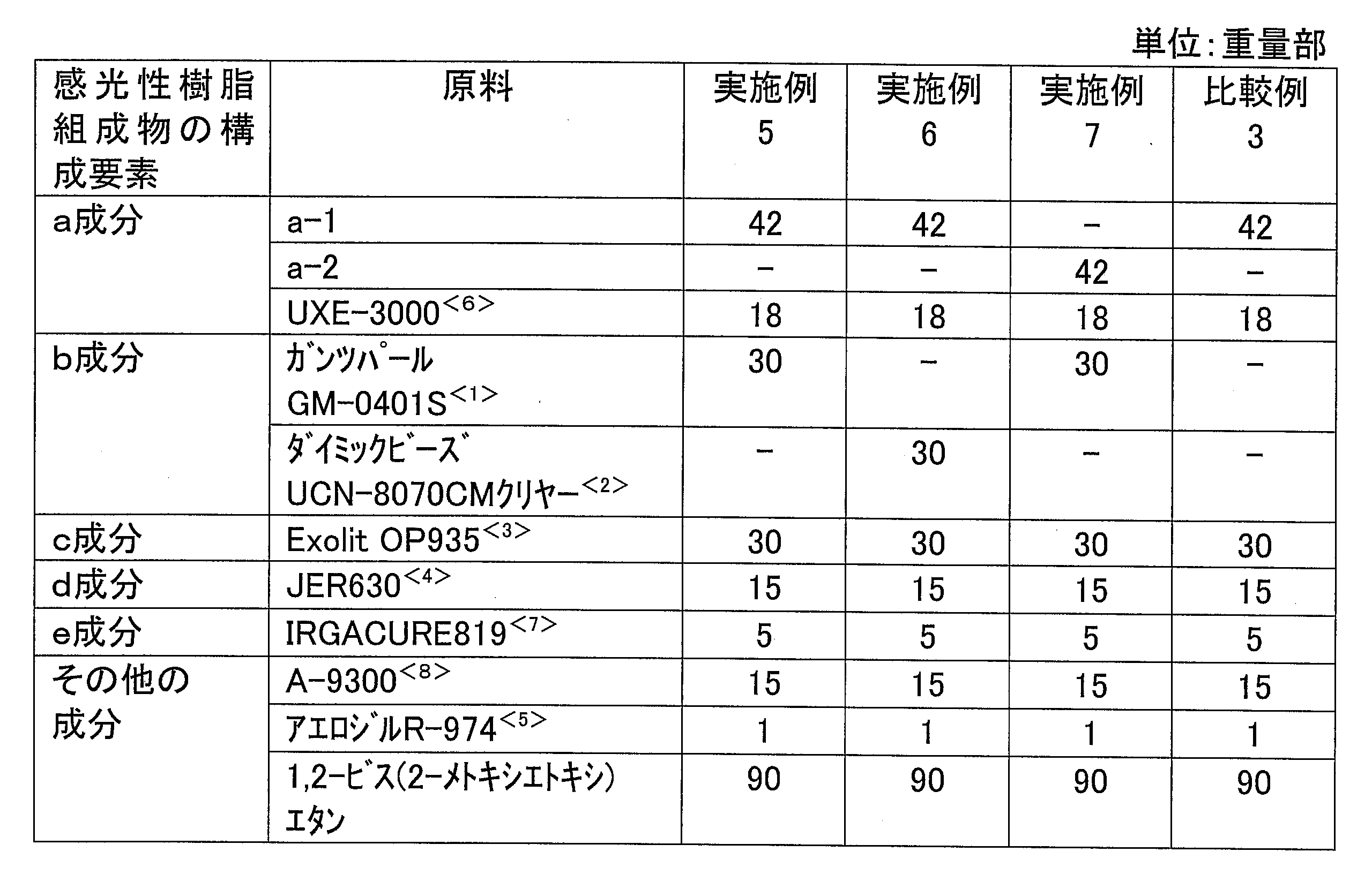
<2>大日精化工業株式会社製 架橋ウレタン系球状有機フィラーの製品名、平均粒子径7μm
<3>クラリアントジャパン株式会社製 リン及びアルミニウム元素を含有する微粒子(ジエチルホスフィン酸アルミニウム塩)の製品名、平均粒子径2.5μm
<4>DIC株式会社製 グリシジルアミン型の多官能エポキシ樹脂の製品名
<5>日本アエロジル株式会社製 シリカ粒子の製品名
<6>日本化薬株式会社製 ウレタン変性エポキシアクリレート樹脂の製品
<7>BASFジャパン株式会社製 光重合開始剤の製品名
<8>新中村化学社製 製品名NKエステルA-9300(エトキシ化イソシアヌル酸トリアクリレート)
<導電層一体型FPC評価試験片の作製>
上記で調整した感光性樹脂組成物を、ベーカー式アプリケーターを用いて、75μmのポリイミドフィルム(株式会社カネカ製:商品名75NPI)に最終乾燥厚みが25μmになるように100mm×100mmの面積に流延・塗布し、80℃で20分乾燥した。次いで、300mJ/cm2の積算露光量の紫外線を照射して露光した。次いで、1.0重量%の炭酸ナトリウム水溶液を30℃に加熱した溶液を用いて、1.0kgf/mm2の吐出圧で90秒スプレー現像を行った。現像後、純水で十分洗浄した後、150℃のオーブン中で30分加熱硬化させて感光性樹脂組成物の絶縁膜を形成し、積層体1を作製した。更に、得られた積層体1の絶縁膜上に、電磁波シールド機能を有する導電層として、フィルムタイプの導電層であるタツタ電線株式会社の商品名SF-PC5500を150℃、2.5MPa、60分の熱プレスによって貼り合せて、導電層一体型FPC評価試験片を作製した。
得られた導電層一体型FPCについて、以下の項目につき評価を行った。評価結果を表4に記載する。
上記<導電層一体型FPC評価試験片の作製>で得られた試験片を用いて、JIS K5400に従って碁盤目テープ法で評価した。
○:碁盤目テープ法で剥がれの無いもの
△:升目の95%以上が残存しているもの
×:升目の残存量が80%未満のもの
(ii)半田耐熱性
上記<導電層一体型FPC評価試験片の作製>で得られた試験片を用いて、260℃で完全に溶解してある半田浴に導電層一体型FPCの導電層面が接する様に浮かべて10秒後に引き上げた。その操作を3回行い、導電層と絶縁膜との接着強度をJIS K5400に従って碁盤目テープ法で評価した。
○:碁盤目テープ法で剥がれの無いもの
△:升目の95%以上が残存しているもの
×:升目の残存量が80%未満のもの
(iii)屈曲性
上記<導電層一体型FPC評価試験片の作製>の項目と同様の方法で、25μm厚みのポリイミドフィルム(株式会社カネカ製アピカル25NPI)表面に感光性樹脂組成物の絶縁膜を形成し、積層体1を作製した。更に、得られた積層体1の絶縁膜上に、電磁波シールド機能を有する導電層として、フィルムタイプの導電層であるタツタ電線株式会社の商品名SF-PC5500を150℃、2.5MPa、60分の熱プレスによって貼り合せて、導電層一体型FPC評価試験片を作製した。得られた試験片を30mm×10mmの短冊に切り出して、15mmのところで180°に10回折り曲げて塗膜を目視で確認してクラックの確認を行った。
○:絶縁膜にクラックが無いもの
△:絶縁膜に若干クラックがあるもの
×:絶縁膜にクラックがあるもの
(iv)反り
上記(iii)屈曲性の項目と同様の方法で得られた試験片を50mm×50mmの面積に切り出して平滑な台の上に導電層面が上面になるように置き、試験片端部の反り高さを測定した。測定部位の模式図を図3に示す。反り量が少ない程、導体層一体型FPCにした場合も反り量が低下することになる。反り量は5mm以下であることが好ましい。
プラスチック材料の難燃性試験規格UL94に従い、以下のように難燃性試験を行った。上記<導電層一体型FPC評価試験片の作製>の項目と同様の方法で、25μm厚みのポリイミドフィルム(株式会社カネカ製アピカル25NPI)片面に感光性樹脂組成物の硬化膜を形成し、積層体1を作製した。更に、得られた積層体1の絶縁膜上に、電磁波シールド機能を有する導電層として、フィルムタイプの導電層であるタツタ電線株式会社の商品名SF-PC5500を150℃、2.5MPa、60分の熱プレスによって貼り合せて、導電層一体型FPC評価試験片を作製した。得られた試験片を寸法:50mm幅×200mm長さに切り出し、125mmの部分に標線を入れ、直径約13mmの筒状に丸め、標線よりも上の重ね合わせ部分(75mmの箇所)、及び、上部に隙間がないようにPIテープを貼り、難燃性試験用の筒を20本用意した。 そのうち10本は(1)23℃/50%相対湿度/48時間で処理し、残りの10本は(2)70℃で168時間処理後無水塩化カルシウム入りデシケーターで4時間以上冷却した。これらのサンプルの上部をクランプで止めて垂直に固定し、サンプル下部にバーナーの炎を10秒間近づけて着火する。10秒間経過したらバーナーの炎を遠ざけて、サンプルの炎や燃焼が何秒後に消えるか測定する。
○:各条件((1)、(2))につき、サンプルからバーナーの炎を遠ざけてから平均(10本の平均)で5秒以内、最高で10秒以内に炎や燃焼が停止し自己消火したもの
×:1本でも10秒以内に消火しないサンプルがあったり、炎がサンプル上部のクランプのところまで上昇して燃焼するもの
(vi)電気絶縁信頼性
フレキシブル金属張積層板(電解銅箔の厚み12μm、ポリイミドフィルムは株式会社カネカ製アピカル25NPI、エポキシ系接着剤で銅箔を接着している)上にライン幅/スペース幅=100μm/100μmの櫛形パターンを作製し、配線パターン付きフィルムを作成した。次いで、上記配線パターン付きフィルムを10容量%の硫酸水溶液中に1分間浸漬した後、純水で洗浄し銅箔の表面処理を行った。その後、上記<導電層一体型FPC評価試験片の作製>の項目と同様の方法で配線パターン付きフィルム上に20μm厚みの感光性樹脂組成物の絶縁膜を片面配線パターン上に形成し、FPCを作製した。更に、得られたFPCの絶縁膜上に、電磁波シールド機能を有する導電層として、フィルムタイプの導電層であるタツタ電線株式会社の商品名SF-PC5500を150℃、2.5MPa、60分の熱プレスによって貼り合せて、導電層一体型FPC評価試験片を作製した。得られた試験片を用いて、40℃、90%RHの環境試験機中で試験片の両端子部分に20Vの直流電流を印加し、絶縁抵抗値の変化やマイグレーションの発生などを観察した。
○:試験開始後、1000時間で10の8乗以上の抵抗値を示し、マイグレーション、デンドライトなどの発生が無いもの。
×:試験開始後、1000時間でマイグレーション、デンドライトなどの発生があるもの。
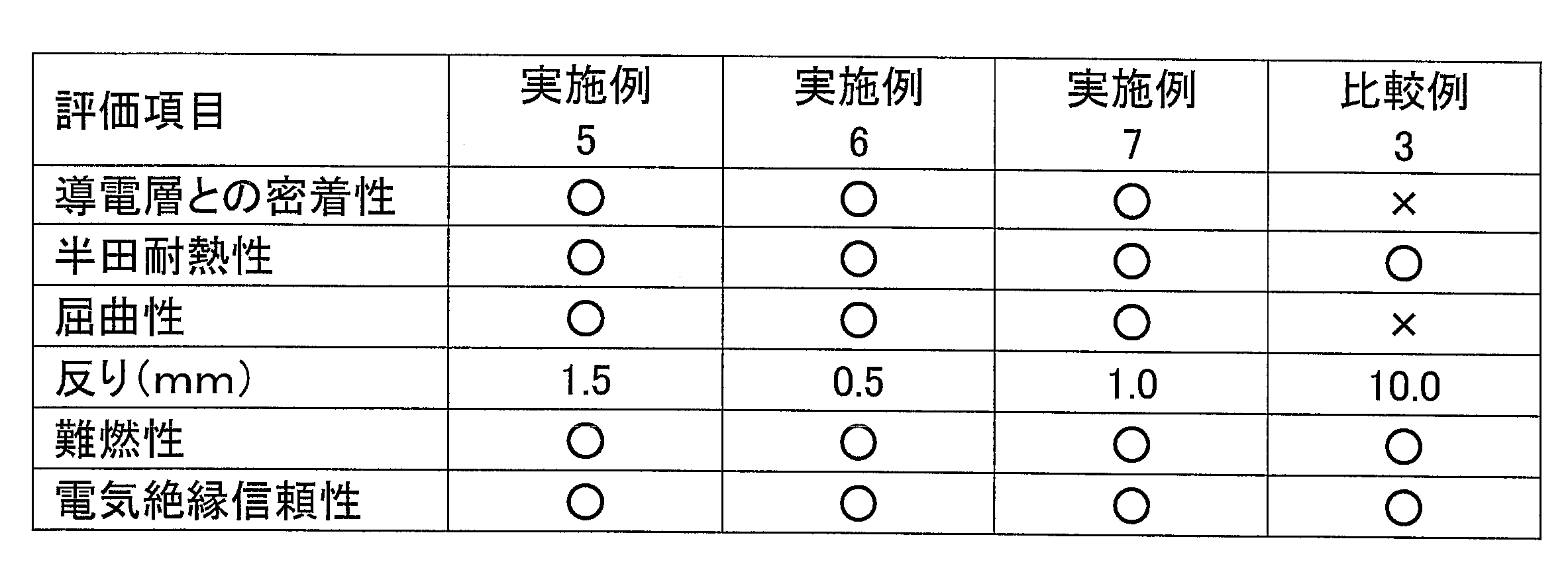
2.配線パターン
3.ベースフィルム
4.絶縁膜
5.FPC
6.電磁波シールド機能を有する導電層
7.測定試料
8.受信用アンテナ
9.送信用アンテナ
10.平滑な台
11.反り量
12.絶縁膜積層フィルム
Claims (5)
- (A)電磁波シールド機能を有する導電層、(B)絶縁膜、(C)配線パターン付きフィルムの順で構成された導電層一体型フレキシブルプリント基板であって、
該(B)絶縁膜が少なくとも(a)バインダーポリマー、及び(b)球状有機ビーズを含有していることを特徴とする導電層一体型フレキシブルプリント基板。 - 上記(B)絶縁膜が、(c)リン、アルミニウム及びマグネシウムからなる群から選ばれる少なくとも1種の元素を含有する微粒子を含有していること特徴とする請求項1に記載の導電層一体型フレキシブルプリント基板。
- 上記(A)電磁波シールド機能を有する導電層が、(f)銀、銅、アルミニウム及びニッケルからなる群から選ばれる少なくとも1種の元素を含有していることを特徴とする請求項1または2に記載の導電層一体型フレキシブルプリント基板。
- 上記(B)絶縁膜が、(d)熱硬化性樹脂を含有している樹脂組成物から得られることを特徴とする請求項1~3のいずれか1項に記載の導電層一体型フレキシブルプリント基板。
- 上記(B)絶縁膜が、(e)光重合開始剤を含有している感光性樹脂組成物から得られることを特徴とする請求項1~4のいずれか1項に記載の導電層一体型フレキシブルプリント基板。
Priority Applications (4)
| Application Number | Priority Date | Filing Date | Title |
|---|---|---|---|
| US14/113,729 US9237645B2 (en) | 2011-04-28 | 2012-04-26 | Flexible printed circuit integrated with conductive layer |
| JP2013512439A JP6106083B2 (ja) | 2011-04-28 | 2012-04-26 | 新規な導電層一体型フレキシブルプリント基板 |
| KR1020137028052A KR101978992B1 (ko) | 2011-04-28 | 2012-04-26 | 신규한 도전층 일체형 플렉서블 프린트 기판 |
| CN201280020477.5A CN103493605B (zh) | 2011-04-28 | 2012-04-26 | 导电层一体型挠性印刷基板 |
Applications Claiming Priority (2)
| Application Number | Priority Date | Filing Date | Title |
|---|---|---|---|
| JP2011-102112 | 2011-04-28 | ||
| JP2011102112 | 2011-04-28 |
Publications (1)
| Publication Number | Publication Date |
|---|---|
| WO2012147870A1 true WO2012147870A1 (ja) | 2012-11-01 |
Family
ID=47072385
Family Applications (1)
| Application Number | Title | Priority Date | Filing Date |
|---|---|---|---|
| PCT/JP2012/061262 Ceased WO2012147870A1 (ja) | 2011-04-28 | 2012-04-26 | 新規な導電層一体型フレキシブルプリント基板 |
Country Status (6)
| Country | Link |
|---|---|
| US (1) | US9237645B2 (ja) |
| JP (1) | JP6106083B2 (ja) |
| KR (1) | KR101978992B1 (ja) |
| CN (1) | CN103493605B (ja) |
| TW (1) | TWI593324B (ja) |
| WO (1) | WO2012147870A1 (ja) |
Cited By (4)
| Publication number | Priority date | Publication date | Assignee | Title |
|---|---|---|---|---|
| CN103367011A (zh) * | 2013-07-17 | 2013-10-23 | 深圳市则成电子工业有限公司 | 一种薄膜开关防泄密方法及一种防泄密薄膜开关 |
| FR3011326A1 (fr) * | 2013-10-02 | 2015-04-03 | Soc Fr Detecteurs Infrarouges Sofradir | Circuit imprime flexible a faible emissivite |
| JP2018010889A (ja) * | 2016-07-11 | 2018-01-18 | 藤森工業株式会社 | 電磁波シールド材 |
| US10317442B2 (en) | 2015-07-31 | 2019-06-11 | Sumitomo Riko Company Limited | Capacitive sensor, sensor sheet, and method for manufacturing capacitive sensor |
Families Citing this family (8)
| Publication number | Priority date | Publication date | Assignee | Title |
|---|---|---|---|---|
| CN104837301A (zh) * | 2014-02-12 | 2015-08-12 | 富葵精密组件(深圳)有限公司 | 具有屏蔽结构的柔性电路板及其制作方法 |
| KR101862121B1 (ko) | 2015-02-02 | 2018-05-29 | 토요잉크Sc홀딩스주식회사 | 전자파 차폐 시트, 프린트 배선판 및 전자 기기 |
| JP6508333B2 (ja) * | 2015-05-14 | 2019-05-08 | 株式会社村田製作所 | 電子回路モジュール |
| WO2017183608A1 (ja) * | 2016-04-19 | 2017-10-26 | 株式会社カネカ | プリント配線板およびその製造方法 |
| TWI689573B (zh) * | 2016-05-23 | 2020-04-01 | 日商拓自達電線股份有限公司 | 導電性接著劑組成物 |
| JP6935807B2 (ja) * | 2017-02-02 | 2021-09-15 | 昭和電工マテリアルズ株式会社 | 電子部品の製造方法、仮保護用樹脂組成物及び仮保護用樹脂フィルム |
| CN109219332A (zh) * | 2017-07-03 | 2019-01-15 | 信越聚合物株式会社 | 电磁波屏蔽膜及其制造方法、以及带有电磁波屏蔽膜的印刷电路板及其制造方法 |
| CN115894882B (zh) * | 2022-11-04 | 2024-02-27 | 常州瑞杰新材料科技有限公司 | 一种性能优良的含硫醚的液晶聚合物及其制备方法 |
Citations (5)
| Publication number | Priority date | Publication date | Assignee | Title |
|---|---|---|---|---|
| JPH0790028A (ja) * | 1993-09-22 | 1995-04-04 | Sekisui Chem Co Ltd | 光重合性組成物、それを用いた接着性テープおよび粘着性テープ |
| JPH07111371A (ja) * | 1993-10-14 | 1995-04-25 | Sharp Corp | フレキシブルプリント基板 |
| JPH1077308A (ja) * | 1996-09-02 | 1998-03-24 | Sekisui Chem Co Ltd | 難燃性光重合性組成物及びこれを用いた難燃性粘着テープ |
| JP2004119445A (ja) * | 2002-09-24 | 2004-04-15 | Matsushita Electric Ind Co Ltd | 薄型電磁シールドおよび薄型電磁シールドが用いられたフレキシブル回路基板 |
| JP2009290103A (ja) * | 2008-05-30 | 2009-12-10 | Tatsuta System Electronics Kk | 電磁波シールド材及びプリント配線板 |
Family Cites Families (13)
| Publication number | Priority date | Publication date | Assignee | Title |
|---|---|---|---|---|
| JPS5212694A (en) * | 1975-07-22 | 1977-01-31 | Tanken Seikou Kk | Carbon sphere |
| US4714623A (en) * | 1985-02-28 | 1987-12-22 | Riccio Louis M | Method and apparatus for applying metal cladding on surfaces and products formed thereby |
| JP2001291961A (ja) * | 2000-04-04 | 2001-10-19 | Ibiden Co Ltd | 多層プリント配線板および多層プリント配線板の製造方法 |
| US6643918B2 (en) | 2000-04-17 | 2003-11-11 | Shielding For Electronics, Inc. | Methods for shielding of cables and connectors |
| US20010033478A1 (en) | 2000-04-21 | 2001-10-25 | Shielding For Electronics, Inc. | EMI and RFI shielding for printed circuit boards |
| JP4295794B2 (ja) * | 2001-06-29 | 2009-07-15 | タツタ電線株式会社 | シールドフレキシブルプリント配線板 |
| JP4514011B2 (ja) * | 2001-09-13 | 2010-07-28 | 日本化薬株式会社 | 樹脂組成物、ソルダーレジスト樹脂組成物及びこれらの硬化物 |
| JP2006229127A (ja) * | 2005-02-21 | 2006-08-31 | Showa Denko Kk | ソルダーレジスト用熱硬化性組成物及びその硬化物 |
| WO2007119513A1 (ja) | 2006-03-29 | 2007-10-25 | Tatsuta System Electronics Co., Ltd. | シールドフィルム及びシールドプリント配線板 |
| JP2009094055A (ja) * | 2007-09-20 | 2009-04-30 | Toray Ind Inc | 電界放出素子用絶縁層の製造方法および電界放出素子基板の製造方法 |
| TWI382519B (zh) * | 2008-04-21 | 2013-01-11 | 日月光半導體製造股份有限公司 | 利用外蓋之電子元件封裝模組 |
| JP5621190B2 (ja) * | 2008-12-15 | 2014-11-05 | 宇部興産株式会社 | 変性ポリイミド樹脂組成物 |
| JP5399803B2 (ja) * | 2009-07-28 | 2014-01-29 | パナソニック株式会社 | 回路基板の製造方法 |
-
2012
- 2012-04-26 US US14/113,729 patent/US9237645B2/en active Active
- 2012-04-26 KR KR1020137028052A patent/KR101978992B1/ko active Active
- 2012-04-26 TW TW101115000A patent/TWI593324B/zh active
- 2012-04-26 JP JP2013512439A patent/JP6106083B2/ja active Active
- 2012-04-26 CN CN201280020477.5A patent/CN103493605B/zh active Active
- 2012-04-26 WO PCT/JP2012/061262 patent/WO2012147870A1/ja not_active Ceased
Patent Citations (5)
| Publication number | Priority date | Publication date | Assignee | Title |
|---|---|---|---|---|
| JPH0790028A (ja) * | 1993-09-22 | 1995-04-04 | Sekisui Chem Co Ltd | 光重合性組成物、それを用いた接着性テープおよび粘着性テープ |
| JPH07111371A (ja) * | 1993-10-14 | 1995-04-25 | Sharp Corp | フレキシブルプリント基板 |
| JPH1077308A (ja) * | 1996-09-02 | 1998-03-24 | Sekisui Chem Co Ltd | 難燃性光重合性組成物及びこれを用いた難燃性粘着テープ |
| JP2004119445A (ja) * | 2002-09-24 | 2004-04-15 | Matsushita Electric Ind Co Ltd | 薄型電磁シールドおよび薄型電磁シールドが用いられたフレキシブル回路基板 |
| JP2009290103A (ja) * | 2008-05-30 | 2009-12-10 | Tatsuta System Electronics Kk | 電磁波シールド材及びプリント配線板 |
Cited By (7)
| Publication number | Priority date | Publication date | Assignee | Title |
|---|---|---|---|---|
| CN103367011A (zh) * | 2013-07-17 | 2013-10-23 | 深圳市则成电子工业有限公司 | 一种薄膜开关防泄密方法及一种防泄密薄膜开关 |
| FR3011326A1 (fr) * | 2013-10-02 | 2015-04-03 | Soc Fr Detecteurs Infrarouges Sofradir | Circuit imprime flexible a faible emissivite |
| WO2015049448A1 (fr) * | 2013-10-02 | 2015-04-09 | Societe Francaise De Detecteurs Infrarouges- Sofradir | Circuit imprime flexible a faible emissivite |
| US10064265B2 (en) | 2013-10-02 | 2018-08-28 | Société Française De Détecteurs Infrarouges—Sofradir | Flexible printed circuit having a low emissivity |
| US10317442B2 (en) | 2015-07-31 | 2019-06-11 | Sumitomo Riko Company Limited | Capacitive sensor, sensor sheet, and method for manufacturing capacitive sensor |
| DE112016000510B4 (de) | 2015-07-31 | 2024-05-08 | Sumitomo Riko Company Limited | Kapazitiver Sensor, Sensorlage und Verfahren zur Herstellung eines kapazitiven Sensors |
| JP2018010889A (ja) * | 2016-07-11 | 2018-01-18 | 藤森工業株式会社 | 電磁波シールド材 |
Also Published As
| Publication number | Publication date |
|---|---|
| US20140054081A1 (en) | 2014-02-27 |
| TW201309112A (zh) | 2013-02-16 |
| US9237645B2 (en) | 2016-01-12 |
| JPWO2012147870A1 (ja) | 2014-07-28 |
| JP6106083B2 (ja) | 2017-03-29 |
| TWI593324B (zh) | 2017-07-21 |
| CN103493605B (zh) | 2017-08-11 |
| KR20140024875A (ko) | 2014-03-03 |
| CN103493605A (zh) | 2014-01-01 |
| KR101978992B1 (ko) | 2019-05-16 |
Similar Documents
| Publication | Publication Date | Title |
|---|---|---|
| JP6106083B2 (ja) | 新規な導電層一体型フレキシブルプリント基板 | |
| JP6106082B2 (ja) | 補強板一体型フレキシブルプリント基板 | |
| JP6134403B2 (ja) | 新規な感光性樹脂組成物及びその利用 | |
| JP6360793B2 (ja) | 導電層一体型フレキシブルプリント基板 | |
| JP6360792B2 (ja) | 補強板一体型フレキシブルプリント基板 | |
| JP5789612B2 (ja) | 新規な感光性樹脂組成物作製キット及びその利用 | |
| US9072177B2 (en) | Conductive layer integrated FPC | |
| JP2009230076A (ja) | 新規な感光性樹脂組成物、それから得られる感光性樹脂組成物溶液、感光性フィルム、絶縁膜及び絶縁膜付きプリント配線板 | |
| JP5858747B2 (ja) | 新規な感光性樹脂組成物作製キット及びその利用 | |
| JP2019012793A (ja) | 導電層一体型フレキシブルプリント基板 | |
| JP5858746B2 (ja) | 新規な感光性樹脂組成物作製キット及びその利用 |
Legal Events
| Date | Code | Title | Description |
|---|---|---|---|
| 121 | Ep: the epo has been informed by wipo that ep was designated in this application |
Ref document number: 12776078 Country of ref document: EP Kind code of ref document: A1 |
|
| ENP | Entry into the national phase |
Ref document number: 2013512439 Country of ref document: JP Kind code of ref document: A |
|
| ENP | Entry into the national phase |
Ref document number: 20137028052 Country of ref document: KR Kind code of ref document: A |
|
| WWE | Wipo information: entry into national phase |
Ref document number: 14113729 Country of ref document: US |
|
| NENP | Non-entry into the national phase |
Ref country code: DE |
|
| 122 | Ep: pct application non-entry in european phase |
Ref document number: 12776078 Country of ref document: EP Kind code of ref document: A1 |