WO2012147472A1 - 化合物半導体単結晶基板およびその製造方法 - Google Patents
化合物半導体単結晶基板およびその製造方法 Download PDFInfo
- Publication number
- WO2012147472A1 WO2012147472A1 PCT/JP2012/059157 JP2012059157W WO2012147472A1 WO 2012147472 A1 WO2012147472 A1 WO 2012147472A1 JP 2012059157 W JP2012059157 W JP 2012059157W WO 2012147472 A1 WO2012147472 A1 WO 2012147472A1
- Authority
- WO
- WIPO (PCT)
- Prior art keywords
- ingot
- single crystal
- compound semiconductor
- wire
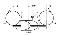
- crystal substrate
- Prior art date
- Legal status (The legal status is an assumption and is not a legal conclusion. Google has not performed a legal analysis and makes no representation as to the accuracy of the status listed.)
- Ceased
Links
Images








Classifications
-
- B—PERFORMING OPERATIONS; TRANSPORTING
- B28—WORKING CEMENT, CLAY, OR STONE
- B28D—WORKING STONE OR STONE-LIKE MATERIALS
- B28D5/00—Fine working of gems, jewels, crystals, e.g. of semiconductor material; apparatus or devices therefor
- B28D5/04—Fine working of gems, jewels, crystals, e.g. of semiconductor material; apparatus or devices therefor by tools other than rotary type, e.g. reciprocating tools
- B28D5/045—Fine working of gems, jewels, crystals, e.g. of semiconductor material; apparatus or devices therefor by tools other than rotary type, e.g. reciprocating tools by cutting with wires or closed-loop blades
-
- B—PERFORMING OPERATIONS; TRANSPORTING
- B23—MACHINE TOOLS; METAL-WORKING NOT OTHERWISE PROVIDED FOR
- B23D—PLANING; SLOTTING; SHEARING; BROACHING; SAWING; FILING; SCRAPING; LIKE OPERATIONS FOR WORKING METAL BY REMOVING MATERIAL, NOT OTHERWISE PROVIDED FOR
- B23D57/00—Sawing machines or sawing devices not covered by one of the preceding groups B23D45/00 - B23D55/00
- B23D57/003—Sawing machines or sawing devices working with saw wires, characterised only by constructional features of particular parts
- B23D57/0046—Sawing machines or sawing devices working with saw wires, characterised only by constructional features of particular parts of devices for feeding, conveying or clamping work
-
- C—CHEMISTRY; METALLURGY
- C30—CRYSTAL GROWTH
- C30B—SINGLE-CRYSTAL GROWTH; UNIDIRECTIONAL SOLIDIFICATION OF EUTECTIC MATERIAL OR UNIDIRECTIONAL DEMIXING OF EUTECTOID MATERIAL; REFINING BY ZONE-MELTING OF MATERIAL; PRODUCTION OF A HOMOGENEOUS POLYCRYSTALLINE MATERIAL WITH DEFINED STRUCTURE; SINGLE CRYSTALS OR HOMOGENEOUS POLYCRYSTALLINE MATERIAL WITH DEFINED STRUCTURE; AFTER-TREATMENT OF SINGLE CRYSTALS OR A HOMOGENEOUS POLYCRYSTALLINE MATERIAL WITH DEFINED STRUCTURE; APPARATUS THEREFOR
- C30B11/00—Single-crystal growth by normal freezing or freezing under temperature gradient, e.g. Bridgman-Stockbarger method
-
- C—CHEMISTRY; METALLURGY
- C30—CRYSTAL GROWTH
- C30B—SINGLE-CRYSTAL GROWTH; UNIDIRECTIONAL SOLIDIFICATION OF EUTECTIC MATERIAL OR UNIDIRECTIONAL DEMIXING OF EUTECTOID MATERIAL; REFINING BY ZONE-MELTING OF MATERIAL; PRODUCTION OF A HOMOGENEOUS POLYCRYSTALLINE MATERIAL WITH DEFINED STRUCTURE; SINGLE CRYSTALS OR HOMOGENEOUS POLYCRYSTALLINE MATERIAL WITH DEFINED STRUCTURE; AFTER-TREATMENT OF SINGLE CRYSTALS OR A HOMOGENEOUS POLYCRYSTALLINE MATERIAL WITH DEFINED STRUCTURE; APPARATUS THEREFOR
- C30B29/00—Single crystals or homogeneous polycrystalline material with defined structure characterised by the material or by their shape
- C30B29/10—Inorganic compounds or compositions
- C30B29/40—AIIIBV compounds wherein A is B, Al, Ga, In or Tl and B is N, P, As, Sb or Bi
- C30B29/42—Gallium arsenide
Definitions
- This invention relates to a compound semiconductor single crystal substrate and a method for manufacturing the same, and more particularly to a compound semiconductor single crystal substrate manufactured from an ingot formed using a horizontal boat method and a method for manufacturing the same.
- Patent Document 1 proposes a technique for reducing the deflection amount of a wire saw in order to suppress a decrease in surface accuracy (for example, flatness and surface roughness) on a cut surface of a workpiece. Specifically, for a wire saw stretched between two rollers, the length of the wire saw located between the surface of the workpiece and the roller is shortened (that is, from the midpoint between the two rollers). It has been proposed to reduce the maximum deflection amount by shifting the arrangement of the workpieces to one roller side.
- an ingot for example, a III-V compound semiconductor single crystal ingot such as GaAs
- a horizontal boat method for example, the horizontal Bridgman method
- the ingot is sliced due to processing space restrictions.
- an inner peripheral cutting machine or a band saw In order to obtain a substrate, it is common to use an inner peripheral cutting machine or a band saw.
- FIG. 15 is a schematic diagram for explaining a process of forming an ingot of a compound semiconductor by a horizontal boat method.
- a raw material of a compound semiconductor is placed in a quartz boat 31, and the raw material in the boat 31 is heated to a melting point or higher by a heater 32 to melt the raw material.
- the compound semiconductor single crystal 34 is grown from the seed crystal 33 side arranged at the end of the boat 31.
- the output of the heater 32 arranged side by side in the longitudinal direction of the boat 31 is locally changed (for example, the heater 32 on the seed crystal 33 side in FIG.
- the heater 32 disposed on the melt 35 side) may have a high output, for example, by gradually moving the boat 31 toward the seed crystal 33 with respect to the heater 32 under such temperature conditions, the seed crystal 33 side. From this, the melt 35 is solidified and a single crystal 34 is grown (the solid-liquid interface 36 between the single crystal 34 and the melt 35 gradually moves away from the seed crystal 33.)
- the ingot thus obtained is As can be seen from FIG. 15, the boat 31 has a curved surface portion along the inner peripheral surface of the boat 31 and a flat free surface.
- the present invention has been made to solve the above-described problems, and an object of the present invention is to reduce the cost of a sufficiently thin compound semiconductor single crystal substrate from an ingot formed by using a horizontal boat method. It is providing the manufacturing method of the compound semiconductor single crystal substrate which can be obtained by this, and the said compound semiconductor single crystal substrate.
- the method of manufacturing a compound semiconductor single crystal substrate according to the present invention includes a step of preparing a single crystal ingot made of a compound semiconductor formed using a horizontal boat method in the (111) direction, and fixing the ingot with a jig.
- the process and the ingot fixed by the jig are reciprocally sent in the (01-1) direction in a (01) direction with a wire saw in a (100) ⁇ 7 ° or (511) ⁇ 7 ° plane orientation. And slicing the ingot fixed by the jig in a direction perpendicular to the reciprocating direction of the wire.
- the ingot can be sliced using a wire saw, so that a compound semiconductor single crystal substrate thinner than the conventional one can be obtained.
- the cutting allowance can be made smaller than when a conventional inner peripheral cutting machine is used. For this reason, since the number of compound semiconductor single crystal substrates that can be cut out from one ingot can be increased, the manufacturing cost of the compound semiconductor single crystal substrate can be reduced.
- the compound semiconductor single crystal substrate according to the present invention is manufactured using the method for manufacturing a compound semiconductor single crystal substrate.
- This compound semiconductor single crystal substrate is thinner than the conventional one and can be manufactured at low cost.
- FIG. 3 is a flowchart illustrating a method for manufacturing a compound semiconductor single crystal substrate according to the present invention. It is a schematic diagram which shows the state which fixed the ingot with the jig
- the manufacturing method of the compound semiconductor single crystal substrate by this invention is demonstrated.
- the compound semiconductor single crystal substrate manufacturing method according to the present invention includes a step of preparing an ingot (S10), a step of fixing with a jig (S20), and a step of slicing the ingot (S30).
- a compound semiconductor grown in the (111) direction by a horizontal boat method is obtained.
- a single crystal ingot can be obtained by cutting the obtained compound semiconductor at, for example, two locations at a plane orientation of (100) ⁇ 7 ° or (511) ⁇ 7 °.
- This ingot is preferably an ingot made of GaAs, and more preferably a silicon-doped GaAs ingot having a carrier concentration of 0.1 ⁇ 10 17 or more and 5.0 ⁇ 10 18 or less.
- the external shape of the ingot 1 obtained by the process (S10) of preparing an ingot is demonstrated.
- the ingot 1 includes a flat free surface 13, a pair of end surfaces 12 that are connected to the free surface 13 and face each other, and a curved side wall 11 that connects the end surfaces 12.
- the end face 12 desirably has a plane orientation of (100) ⁇ 7 ° or (511) ⁇ 7 °.
- the two end faces 12 facing each other may have the same plane orientation or different plane orientations, but desirably have the same plane orientation.
- the boundary portion with the free surface 13 has a linear outer peripheral line, and the outer peripheral portion that is the boundary portion with the side wall 11 is curved.
- the side wall 11 extends in a direction inclined with respect to the end surface 12.
- FIG. 2 is a schematic diagram showing a state in which the ingot 1 is fixed using a jig.
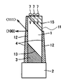
- FIG. 3 schematically shows a cross section taken along line III-III in FIG. 2, and the ingot 1 and the jig for fixing the ingot 1 are fixed.
- a tool hereinafter sometimes referred to as a fixing jig is shown.
- the hook fixing jig is not particularly limited as long as the ingot 1 can be fixed thereby, but preferably includes a supporting member 2 and a lower auxiliary plate 3 and a side auxiliary plate 4 on the upper surface thereof.
- the lower auxiliary plate 3 is disposed on the upper surface of the support member 2.
- the lower auxiliary plate 3 has substantially the same width as the free surface 13 of the ingot 1.
- the pair of end surfaces 12 of the ingot 1 are disposed perpendicular to the upper surface of the support member 2, and the free surface 13 is disposed so as to face the upper surface of the support member 2.
- the upper surface of the lower auxiliary plate 3 is formed so as to extend in a direction along the inclined free surface 13.
- the upper surface of the lower auxiliary plate 3 is connected and fixed to the free surface 13 of the ingot 1. By doing in this way, it can prevent that the compound semiconductor single crystal substrate cut out is separated after slicing.
- the side auxiliary plate 4 is arranged so as to sandwich the ingot 1 from the end surface 12 side and in contact with the end surface 12.
- the lower portion of the side auxiliary plate 4 is in contact with the side surface of the lower auxiliary plate 3.
- the width of the side auxiliary plate 4 is substantially the same as the width of the end surface 12 of the ingot 1.
- the ingot 1 is fixed by the lower auxiliary plate 3 and the side auxiliary plate 4 arranged on the upper surface of the support member 2.
- the side surface auxiliary plate 4 is important as a measure against disconnection of the wire 7.
- the side auxiliary plate 4 has a relatively thicker thickness on the lower auxiliary plate 3 side and becomes thinner toward the upper side. That is, the side auxiliary plate 4 has a tapered outer peripheral side surface, and the inner peripheral side surface of the side auxiliary plate 4 on the ingot 1 side extends perpendicularly to the upper surface of the support member 2.
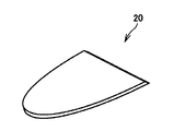
- a step (S30) of slicing the fixed ingot is performed. Specifically, as shown in FIGS. 4 to 6, the ingot 1 is sliced using a wire saw to obtain a compound semiconductor single crystal substrate 20 as shown in FIG.
- the wire saw for example, a workpiece raising type wire saw can be used.
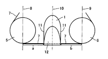
- the wire saw includes a wire 7 for cutting the ingot 1, a pair of guide rollers 5, 6 for positioning the wire 7 while laying the wire 7 and applying tension to the wire 7, 6 is provided with a drive unit (not shown) for driving 6 and a moving mechanism (not shown) for moving an ingot as a workpiece relative to the wire 7.
- the ingot 1 is cut by a wire 7 stretched between the guide rollers 5 and 6.
- the ingot 1 is arranged so that the center axis 10 of the ingot 1 is positioned at an intermediate point between the center line 8 of the guide roller 5 and the center line 9 of the other guide roller 6.
- the boundary line (the lower end of the ingot 1 in FIG. 4) indicating the boundary between the free surface 13 (see FIG. 3) and the end surface 12 of the ingot 1 is parallel to the extending direction of the wire 7 located between the guide rollers 5 and 6. Is arranged. From a different point of view, a plane that passes through an intermediate point between the pair of guide rollers 5 and 6 and extends in a direction perpendicular to the extending direction of the wire 7 (on the paper surface of FIG. 4 including the central axis 10).
- the ingot 1 is arranged so that the outer shape of the ingot 1 is symmetrical with respect to a plane that is a vertical plane.
- the distance c in FIG. 5 corresponding to the distance a shown in FIG. 4 and the distance d in FIG. 5 corresponding to the distance b in FIG. become.
- the deflection amounts of the wires 7 positioned on the left and right sides of the ingot 1 are not substantially different on the left and right sides, and are substantially the same. Therefore, the shape accuracy and surface accuracy of the cut-out compound semiconductor single crystal substrate 20 are improved. Can keep.
- the shape of the side wall 11 of the ingot 1 is the central axis shown in FIGS.
- the wire 7 is symmetric in the extending direction about 10. Therefore, as shown in FIG. 6, when the ingot 1 is sliced into a plurality of substrates at a time, the above relationship is established for each wire 7 slicing the ingot 1. Specifically, the distance e in FIG. 6 corresponding to the distance a shown in FIG. 4 and the distance f in FIG. 6 corresponding to the distance b in FIG. 4 are kept the same. Similarly, the distance g and the distance h in FIG. 6 are also kept the same.
- the compound semiconductor single crystal substrate 20 is performed by subjecting each of the obtained compound semiconductor single crystal substrates to an end face treatment, a surface polishing treatment, a cleaning treatment, and the like. Can be obtained.
- Compound semiconductor single crystal substrate 20 has a thickness of, for example, 300 ⁇ m or less, and a warpage amount of, for example, 15 ⁇ m or less.
- the amount of warpage of the compound semiconductor single crystal substrate 20 refers to the maximum waviness of filtering W CM (specified in JIS B0610).
- This compound semiconductor single crystal substrate can be used for manufacturing infrared LEDs and the like.
- an additional auxiliary member may be attached to the ingot 1 in the step of fixing with a jig (S20).
- the additional auxiliary member may be an upper auxiliary plate 15 attached on the ingot 1 as shown in FIG. 8 (FIG. 8 corresponds to FIG. 3), for example.
- the upper auxiliary plate 15 is disposed on the upper portion of the side wall 11 of the ingot 1 (that is, the surface of the ingot 1 with which the wire 7 first contacts). Further, in the slicing step (S30), the wire 7 comes into contact with the surface of the upper auxiliary plate 15 prior to the ingot 1.
- the upper auxiliary plate 15 is parallel to the plane perpendicular to the moving direction of the wire 7 relative to the ingot (arrow in FIG. 8) along the extending direction of the wire 7. Further, the surface of the upper auxiliary plate 15 is formed to be parallel to the upper surface of the support member 2 (that is, to extend in the horizontal direction) when placed on the upper portion of the ingot 1. The surface of the upper auxiliary plate 15 that faces the side wall 11 is an inclined surface that extends in the same direction as the side wall 11.
- the wire 7 is first cut into the inclined side wall 11, and the position of the wire 7 may be shifted at the time of the cutting (the wire 7 undulates). There is). This is because the direction of the side wall 11 is inclined with respect to the cutting direction of the wire 7 (downward direction in FIG. 3) (for example, it is inclined by 54.7 °). It happens because you can't bite.
- the upper auxiliary plate 15 by attaching the upper auxiliary plate 15, it is possible to prevent the displacement of the position of the wire 7 at the time of cutting.
- the lower auxiliary plate 3, the side auxiliary plate 4, and the upper auxiliary plate 15 can be formed of any material, but preferably carbon can be used. Carbon is suitable as a material for such a jig because it is inexpensive and easy to process.
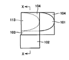
- FIG. 10 which is a schematic cross-sectional view taken along the line XX of FIG. 9, the effect of the method for manufacturing the compound semiconductor single crystal substrate of the embodiment of the present invention will be described.
- the orientation of the ingot with respect to the cutting direction of the wire saw was rotated by 90 ° from the position of the ingot according to the embodiment of the present invention.
- an ingot 101 having the same shape as that of the embodiment of the present invention is prepared.
- the step of fixing to the jig (S20) the ingot 101 is fixed by the jig.
- a rectangular parallelepiped lower auxiliary plate 103 is disposed on the upper surface of the support member 102, and the ingot 101 is disposed on the lower auxiliary plate 103.
- the ingot 101 is arranged such that its free surface 113 extends in a direction perpendicular to the upper surface of the lower auxiliary plate 103. That is, the ingot 101 is arranged so that the side wall thereof is in contact with the upper surface of the lower auxiliary plate 103.
- assistant board 104 is arrange
- the ingot 101 is cut using a wire saw.
- the center axis 110 (specifically, as shown in FIG. 9) of the ingot 101 fixed by the fixing jig in the direction along which the wire 7 extends at the time of cutting.
- a line segment passing through the center of the ingot 101 in the width direction and perpendicular to the upper surface of the support member 102 is considered.
- the central axis 110 passes through the intermediate point between the center lines 8 and 9 of the guide rollers 5 and 6.
- An ingot 101 is arranged. In this case, as shown in FIG.
- Distance a (that is, the length of the wire 7 positioned on the guide roller 5 side of the ingot 101) is the distance between the surface of the ingot 101 and the position where the wire 7 is separated from the surface of the guide roller 6 (that is, the position of the center line 9).
- the distance b the length of the wire 7 positioned on the guide roller 6 side of the ingot 101
- the length is almost always different when the ingot 101 is cut. For example, as shown in FIG.
- the distance c shown in FIG. 12 corresponding to the distance a shown in FIG. 11 and the distance b shown in FIG. It is different from the distance d. That is, the ratio (a / b) between the distance a and the distance b or the ratio (c / d) between the distance c and the distance d changes as the cutting of the ingot 101 proceeds.
- the surface shape of the cut substrate is adversely affected. That is, as the length of the portion of the wire 7 exposed on the left and right sides of the ingot 101 is longer, the deflection of the wire 7 can be increased. And as shown in FIG. 11, the lengths of the portions of the wire 7 exposed on the left and right sides of the ingot 101 (distance a and distance b in FIG. 11, distance c and distance d in FIG. 12) are different. This means that the contact angle and pressure conditions at the contact portion between the wire 7 and the ingot 101 on the left and right sides of the ingot 101 are different.
- the length of the exposed wire 7 on the left and right sides of the ingot 101 changes as the cutting of the ingot 101 proceeds.
- the contact angle and pressure conditions described above also change as cutting progresses.
- characteristics such as the surface properties and warpage of the cut substrate vary.
- the warpage and the surface state are different among the plurality of obtained substrates.
- the ratio of the lengths of the wires 7 exposed on the left and right sides of the ingot 101 are different in a plurality of substrates.
- the ratio of the distance e and the distance f related to an arbitrary substrate in the thickness direction of the ingot 101 in FIG. 13 is different from the ratio of the distance g and the distance h related to another substrate in the thickness direction. .
- the compound semiconductor single crystal substrate 20 with good shape accuracy can be obtained as described with reference to FIGS.
- the method for manufacturing a compound semiconductor single crystal substrate according to the present invention includes a step (S10) of preparing an ingot 1 made of a compound semiconductor single crystal formed by using a horizontal boat method, and fixing the ingot 1 with a jig.
- tool using a wire saw are provided.
- a compound semiconductor formed in the (111) direction is obtained by a horizontal boat method, and this is preferably obtained in a plane orientation of (100) ⁇ 7 ° or (511) ⁇ 7 °.
- a single crystal ingot is obtained by cutting two places.
- the single crystal ingot is fixed with a fixing jig (support member 2, lower auxiliary plate 3, side auxiliary plate 4).
- the ingot 1 fixed by the jig is sliced in a plane orientation of (100) ⁇ 7 ° or (511) ⁇ 7 ° using a wire saw. This is performed by raising the ingot 1 fixed by the jig in a direction perpendicular to the reciprocating direction of the wire 7 while feeding the wire 7 of the wire saw back and forth in the (01-1) direction of the ingot 1.
- the said ingot 1 is used using a wire saw. Since slicing is performed, a compound semiconductor single crystal substrate 20 thinner than the conventional one can be obtained. Moreover, since the ingot 1 is sliced using a wire saw, the cutting allowance can be made smaller than when a conventional inner peripheral cutting machine is used. For this reason, since the number of compound semiconductor single crystal substrates 20 that can be cut out from one ingot can be increased, the manufacturing cost of the compound semiconductor single crystal substrate 20 can be reduced.
- a wire saw (wire 7) stretched between a pair of rollers (guide rollers 5, 6) may be used.
- the ingot 1 passes through an intermediate point between the pair of guide rollers 5 and 6 and extends in a direction perpendicular to the extending direction of the wire saw (wire 7) (see FIG. In FIG. 4, the ingot 1 may be sliced after being arranged so that the outer shape of the ingot 1 is symmetrical with respect to a plane that passes through the central axis 10 and is perpendicular to the paper surface.
- the lengths of the portions of the wire 7 on the left and right sides of the ingot 1 can be the same.
- the amount of deflection at the portion of the wire 7 can also be made substantially the same on the left and right sides of the ingot 1.
- the step of fixing with a jig S20
- An auxiliary member (upper auxiliary plate 15) may be disposed.
- the surface of the upper auxiliary plate 15 that first contacts the wire 7 is along the extending direction of the wire 7 and with respect to the moving direction of the wire 7 (downward direction in FIG. 8). It may be parallel to a vertical plane.
- the ingot 1 may include a free surface 13 that does not contact the container during crystal growth.
- the ingot 1 in the slicing step (S30), as shown in FIGS. 2 to 5, the ingot 1 is arranged so that the free surface 13 extends in a direction along the extending direction of the wire saw (wire 7). May be. In this case, it is possible to obtain the compound semiconductor single crystal substrate 20 with less thickness variation and less warping.
- the compound semiconductor single crystal substrate 20 according to the present invention is manufactured using the compound semiconductor single crystal substrate manufacturing method. In this way, the compound semiconductor single crystal substrate 20 can be realized at a lower cost and with a thinner thickness than the conventional one.
- the compound semiconductor single crystal substrate 20 may have a thickness of 300 ⁇ m or less. Since the thickness can be made thinner than the compound semiconductor single crystal substrate obtained by slicing the ingot 1 using an inner peripheral cutting machine as in the prior art, the number of compound semiconductor single crystal substrates obtained from one ingot is conventionally increased. You can do more. That is, the compound semiconductor single crystal substrate 20 can be obtained at low cost.
- the warpage of the compound semiconductor single crystal substrate 20 may be 15 ⁇ m or less. In this case, since it has good flatness, a high-quality semiconductor layer can be epitaxially grown on the main surface.
- a GaAs crystal ingot was fixed by a support member 2, a lower auxiliary plate 3, and a side auxiliary plate 4 as shown in FIGS.
- the size of the ingot the height of the end face 12 of the ingot shown in FIG. 3 is 70 mm, and the width of the ingot shown in FIG. 2 is 75 mm.
- an ingot made of GaAs crystal having the same shape and size was prepared and fixed by a support member 102, a lower auxiliary plate 103, and a side auxiliary plate 104 as shown in FIGS.
- the ingot fixed by the fixing jig described above was sliced using a wire saw.
- the conditions for slicing with a wire saw are as follows. That is, U400 manufactured by Yasunaga Co., Ltd. was used as the equipment, and a saw wire with a brass plating diameter of 120 ⁇ m was used as the wire (saw wire).
- the abrasive grains contained were GC # 1200
- the oil was oily oil
- the blending ratio of abrasive grains to oil was 1.111 kg of abrasive grains per liter of oil.
- the processing speed was 150 ⁇ m / min
- the wire feed amount was 15 m / min
- the wire average linear velocity was 320 m / min.
- the method of measuring the warpage amount in accordance with the method of measuring the filtered maximum waviness W CM prescribed in JISB0610.
- the measurement results are shown in FIG.
- the horizontal axis of the graph shown in FIG. 14 indicates the position (ingot position) where the substrate is collected in the ingot, and the vertical axis indicates the amount of warpage (unit: ⁇ m) of the substrate.
- circles in the graph are data related to the samples of the examples of the present invention, and square marks are data related to the samples of the comparative examples.
- the position of the ingot on the horizontal axis is the position of one end face 12 (end face 112 shown in FIG. 10) of the ingot 1 (or ingot 101 shown in FIG. 10) shown in FIG.
- the other end face 12 (or the end face 112) was taken as (b) in FIG. 14, and the amount of warpage was measured for a plurality of substrates taken from (a) to (b) in the thickness direction of the ingot.
- the warpage value regarding the sample of the example of the present invention is smaller than the warpage value regarding the sample of the comparative example as a whole. That is, according to the method for manufacturing a compound semiconductor single crystal substrate according to the present invention, the warpage of the obtained substrate is reduced over the entire position of the ingot as compared with the method of the comparative example.
- the present invention is particularly advantageously applied to a method of manufacturing a compound semiconductor single crystal substrate using an ingot formed by a horizontal boat method.
Landscapes
- Chemical & Material Sciences (AREA)
- Engineering & Computer Science (AREA)
- Mechanical Engineering (AREA)
- Crystallography & Structural Chemistry (AREA)
- Materials Engineering (AREA)
- Metallurgy (AREA)
- Organic Chemistry (AREA)
- Inorganic Chemistry (AREA)
- Mechanical Treatment Of Semiconductor (AREA)
- Crystals, And After-Treatments Of Crystals (AREA)
- Processing Of Stones Or Stones Resemblance Materials (AREA)
- Finish Polishing, Edge Sharpening, And Grinding By Specific Grinding Devices (AREA)
Abstract
水平ボート法を用いて形成されたインゴットから十分な薄さの化合物半導体基板を低コストで得ることが可能な化合物半導体単結晶基板の製造方法および当該化合物半導体単結晶基板を提供する。化合物半導体単結晶基板の製造方法は、(111)方向に水平ボート法を用いて形成された化合物半導体からなる単結晶インゴット1を準備する工程と、当該インゴット1を治具により固定する工程と、治具により固定されたインゴット1を、ワイヤソーを用いて(100)±7°または(511)±7°の面方位で、ワイヤソーのワイヤ7を(01-1)方向に往復に送りながら、治具により固定されたインゴット1をワイヤ7の往復方向と直行する方向に上昇させて、ワイヤ7を用いてスライスする工程とを備える。
Description
この発明は、化合物半導体単結晶基板およびその製造方法に関し、より特定的には、水平ボート法を用いて形成されたインゴットから製造される化合物半導体単結晶基板およびその製造方法に関する。
従来、化合物半導体単結晶基板を製造するために、半導体からなるインゴットをスライス加工する方法としてワイヤソーを用いた加工方法が知られている(たとえば、特開2007-54909号公報(特許文献1)参照)。特許文献1では、被加工物の切断面における面精度(たとえば平面度や面粗さなど)の低下を抑制するため、ワイヤソーのたわみ量を低減する技術が提案されている。具体的には、2つのローラの間に掛け渡されたワイヤソーについて、被加工物の表面とローラとの間に位置するワイヤソーの長さを短くする(つまり、2つのローラの間の中間点から被加工物の配置を一方のローラ側にずらす)ことにより、最大たわみ量を小さくすることが提案されている。
一方、水平ボート法(例えば水平ブリッジマン法など)を用いて形成されたインゴット(たとえばGaAsなどのIII-V族化合物半導体単結晶インゴット)については、加工スペースの制約などにより、当該インゴットをスライスして基板を得るために内周刃切断機やバンドソーを用いることが一般的である。
例えば、以下に説明するような水平ボート法によりインゴットを形成することができる。図15は水平ボート法により化合物半導体のインゴットを形成する工程を説明するための模式図である。図15に示すように、水平ボート法では、たとえば石英製のボート31の内部に化合物半導体の原料を入れ、ヒータ32によって当該ボート31内の原料を融点以上に加熱して原料を融解する。その後、ボート31の長手方向に沿って温度勾配を形成することで、ボート31の端部に配置した種結晶33側から化合物半導体の単結晶34を成長させる。温度勾配の形成方法としては、ボート31の長手方向に並んで配置されるヒータ32の出力を局所的に変更する(たとえば、図15の種結晶33側のヒータ32は低出力とし、反対側(融液35側)に配置されたヒータ32を高出力としてもよい。このような温度条件で、たとえばヒータ32に対してボート31を種結晶33側に徐々に移動させることにより、種結晶33側から融液35が固化し単結晶34が成長する(単結晶34と融液35との固液界面36が徐々に種結晶33から離れる方向に移動する)。このようにして得られたインゴットは、図15からも分かるようにボート31の内周表面に沿った曲面状の表面部分と、平坦なフリー面とを有する。
上述した水平ボート法を用いて形成されたインゴットをスライスするために、たとえば内周刃切断機を用いた場合、得られる基板の厚みを薄くすることには限界がある。たとえば内周刃切断機により300μm以下の厚みの基板を切り出すことは難しかった。これは、このような薄い基板を、内周刃切断機を用いて切り出す場合には、インゴットの切断中に基板の欠けや割れが発生する場合が多いためである。特に、シリコンドープのIII-V族化合物半導体インゴットでキャリア濃度が高いもの(例えばキャリア濃度が1.0×10¹⁸以上)を切り出すことは難しかった。これは、シリコンのドーピング量が高くなるほど結晶の異方性が強く劈開性が大きくなるためだと考えられる。
また、当該インゴットを薄くスライスするために、特許文献1に開示されるようなワイヤソーを用いる方法は従来適用されていなかった。これは、図15からも分かるように、水平ボート法を用いて形成されたインゴットが、チョクラルスキー法を用いて形成されたシリコンインゴットのような円柱状といった単純な形状ではないことも一因であると考えられる。つまり、従来は水平ボート法を用いて形成されたインゴットを十分薄くスライスすることは困難であった。さらに、上記のような内周刃切断機などを用いてインゴットをスライスする場合、切り代がワイヤソーなどを用いた場合より大きくなる。すなわち、同じ大きさのインゴットから切り出せる基板の枚数が、ワイヤソーより内周刃切断機などを用いた場合の方が少なくなる。この結果、製造コストが増大することになっていた。
一方、近年は材料コストの低減が要求されるため、基板の厚みを減少することや、切り出し時の切り代の低減が求められている。
この発明は、上記のような課題を解決するためになされたものであり、この発明の目的は、水平ボート法を用いて形成されたインゴットから十分な薄さの化合物半導体単結晶基板を低コストで得ることが可能な化合物半導体単結晶基板の製造方法および当該化合物半導体単結晶基板を提供することである。
この発明に従った化合物半導体単結晶基板の製造方法は、(111)方向に水平ボート法を用いて形成された化合物半導体からなる単結晶インゴットを準備する工程と、当該インゴットを治具により固定する工程と、治具により固定された前記インゴットを、ワイヤソーを用いて(100)±7°または(511)±7°の面方位で、ワイヤソーのワイヤを(01-1)方向に往復に送りながら、治具により固定されたインゴットをワイヤの往復方向と直行する方向に上昇させてスライスする工程とを備える。
このように、水平ボート法を用いて形成されたインゴットを治具で固定することにより、ワイヤソーを用いて当該インゴットをスライスすることができるので、従来より薄い化合物半導体単結晶基板を得ることができる。また、ワイヤソーを用いてインゴットをスライスするため、従来の内周刃切断機などを用いた場合より切り代を小さくできる。このため、1つのインゴットから切り出せる化合物半導体単結晶基板の枚数を増やすことができるので、当該化合物半導体単結晶基板の製造コストを低減できる。
この発明に従った化合物半導体単結晶基板は、前記化合物半導体単結晶基板の製造方法を用いて製造されたものである。この化合物半導体単結晶基板は、従来よりも厚みが薄く、低コストで製造できる。
本発明によれば、従来より薄く、低コストの化合物半導体単結晶基板を得ることができる。
以下、図面に基づいて本発明の実施の形態を説明する。なお、以下の図面において同一または相当する部分には同一の参照番号を付しその説明は繰返さない。
図1を参照して、本発明による化合物半導体単結晶基板の製造方法を説明する。
図1に示すように、本発明による化合物半導体単結晶基板の製造方法は、インゴットを準備する工程(S10)、治具で固定する工程(S20)及びインゴットをスライスする工程(S30)を含む。
図1に示すように、本発明による化合物半導体単結晶基板の製造方法は、インゴットを準備する工程(S10)、治具で固定する工程(S20)及びインゴットをスライスする工程(S30)を含む。
インゴットを準備する工程(S10)において、まず、水平ボート法によって(111)方向に成長させた化合物半導体を得る。得られた化合物半導体を、たとえば面方位(100)±7°または(511)±7°で、2箇所切断することにより単結晶インゴットを得ることができる。このインゴットは、好ましくは、GaAsからなるインゴットであり、さらに好ましくはキャリア濃度が0.1×10¹⁷以上5.0×10¹⁸以下のシリコンドープGaAsインゴットである。
図2を参照して、インゴットを準備する工程(S10)で得られるインゴット1の外形について説明する。インゴット1は、平坦なフリー面13と、このフリー面13に連なり、互いに対向する1組の端面12と、この端面12の間をつなぐ曲面状の側壁11とからなる。端面12は、(100)±7°または(511)±7°の面方位を有していることが望ましい。また、対向する2つの端面12は、同じ面方位を有していてもよいし、異なる面方位であってもよいが、望ましくは同じ面方位を有する。端面12において、フリー面13との境界部は直線状の外周線を有しており、側壁11との境界部である外周部は曲線状になっている。側壁11は端面12に対して傾斜した方向に延びている。
図2を参照して、インゴットを準備する工程(S10)で得られるインゴット1の外形について説明する。インゴット1は、平坦なフリー面13と、このフリー面13に連なり、互いに対向する1組の端面12と、この端面12の間をつなぐ曲面状の側壁11とからなる。端面12は、(100)±7°または(511)±7°の面方位を有していることが望ましい。また、対向する2つの端面12は、同じ面方位を有していてもよいし、異なる面方位であってもよいが、望ましくは同じ面方位を有する。端面12において、フリー面13との境界部は直線状の外周線を有しており、側壁11との境界部である外周部は曲線状になっている。側壁11は端面12に対して傾斜した方向に延びている。
次に、インゴットを治具で固定する工程(S20)を実施する。図2は、インゴット1を、治具を用いて固定した状態を示す模式図であり、図3は、図2のIII-III線の断面を模式的に示し、インゴット1とこれを固定する治具(以下、固定用治具という場合がある)を示す。
固定用治具は、それによりインゴット1を固定することができれば特に限定されないが、好ましくは、支持部材2と、その上部表面上に下部補助板3および側面補助板4を含む。具体的には、支持部材2の上部表面上に下部補助板3が配置される。下部補助板3はインゴット1のフリー面13とほぼ同じ幅である。そして、インゴット1の1組の端面12を支持部材2の上部表面に対して垂直に配置するとともに、フリー面13が支持部材2の上部表面と対向するように配置する。この場合、下部補助板3の上部表面は、傾斜したフリー面13に沿った方向に延びるように形成されている。下部補助板3の上部表面は、インゴット1のフリー面13と接続固定されている。このようにすることで、切り出された化合物半導体単結晶基板がスライス後にばらばらになることを防止できる。
また、側面補助板4は、インゴット1を端面12側から挟むように、また端面12に接触するように配置されている。側面補助板4の下部は、下部補助板3の側面と接触している。図2から分かるように、側面補助板4の幅はインゴット1の端面12の幅とほぼ同じになっている。このように、支持部材2の上部表面上に配置された下部補助板3および側面補助板4によりインゴット1が固定される。なお、側面補助板4は、ワイヤ7の断線対策として重要である。なお、側面補助板4は図3から分かるように、下部補助板3側での厚みが相対的に厚く、上部に向かうほどその厚みが薄くなる。つまり、側面補助板4はテーパー状の外周側面を有し、かつ、側面補助板4におけるインゴット1側の内周側面は支持部材2の上部表面に対して垂直に延びている。
次に、固定したインゴットをスライスする工程(S30)を実施する。具体的には、図4~図6に示すように、ワイヤソーを用いてインゴット1をスライスすることにより、図7に示すような化合物半導体単結晶基板20を得る。
前記ワイヤソーとしては、たとえば加工対象物上昇型のワイヤソーを用いることができる。ワイヤソーは、インゴット1を切断するためのワイヤ7と、ワイヤ7を掛け渡してワイヤ7の位置決めを行なうとともにワイヤ7に張力を付加するための1組のガイドローラ5、6と、ガイドローラ5、6を駆動するための駆動部(図示せず)と、加工対象物であるインゴットをワイヤ7に対して相対的に移動させるための移動機構(図示せず)とを備える。
インゴット1は、図4および図5に示すように、ガイドローラ5、6の間に張られたワイヤ7によって切断される。このとき、ガイドローラ5の中心線8と、もう一方のガイドローラ6の中心線9との間の中間点にインゴット1の中心軸10が位置するように、インゴット1を配置する。インゴット1のフリー面13(図3参照)と端面12との境界を示す境界線(図4のインゴット1の下端)は、ガイドローラ5、6の間に位置するワイヤ7の延びる方向と平行に配置されている。また、異なる観点から言えば、1対のガイドローラ5、6の間の中間点を通るとともにワイヤ7の延在方向に対して垂直な方向に伸びる平面(中心軸10を含む図4の紙面に垂直な平面)を対称面とした面対称にインゴット1の外形がなるように、インゴット1は配置されている。
インゴット1は、図4および図5に示すように、ガイドローラ5、6の間に張られたワイヤ7によって切断される。このとき、ガイドローラ5の中心線8と、もう一方のガイドローラ6の中心線9との間の中間点にインゴット1の中心軸10が位置するように、インゴット1を配置する。インゴット1のフリー面13(図3参照)と端面12との境界を示す境界線(図4のインゴット1の下端)は、ガイドローラ5、6の間に位置するワイヤ7の延びる方向と平行に配置されている。また、異なる観点から言えば、1対のガイドローラ5、6の間の中間点を通るとともにワイヤ7の延在方向に対して垂直な方向に伸びる平面(中心軸10を含む図4の紙面に垂直な平面)を対称面とした面対称にインゴット1の外形がなるように、インゴット1は配置されている。
このようにすれば、図4に示すように、インゴット1のスライス時において、インゴット1の表面と、ガイドローラ5側のワイヤ7がガイドローラ5の表面から離れる位置(すなわち上述した中心線8の位置)との間の距離a(すなわちインゴット1のガイドローラ5側にあるワイヤ7の長さ)は、インゴット1の表面と、ガイドローラ6の表面からワイヤ7が離れる位置(すなわち中心線9の位置)との間の距離b(インゴット1のガイドローラ6側にあるワイヤ7の長さ)と同じになる。そして、上記のようにインゴット1の位置がワイヤ7に対して設定されていることから、上記のようなインゴット1の左右におけるワイヤ7の長さの関係はスライスする工程の間維持される。
たとえば、図5に示すように、スライスする工程の別の時点において、図4に示した距離aに対応する図5の距離cと、図4の距離bに対応する図5の距離dは同じになる。
以上のように、インゴット1を挟んで左右に位置するワイヤ7のたわみ量が左右で大きく異ならず、ほぼ同じになるので、切り出された化合物半導体単結晶基板20の形状精度や面精度を良好に保つことができる。
以上のように、インゴット1を挟んで左右に位置するワイヤ7のたわみ量が左右で大きく異ならず、ほぼ同じになるので、切り出された化合物半導体単結晶基板20の形状精度や面精度を良好に保つことができる。
図6に示すように、インゴット1をその上方(スライス時のインゴット1の移動経路の終点側)から見た場合に、インゴット1の側壁11の形状は、図4や図5に示した中心軸10を中心としてワイヤ7の延在方向において対称になっている。そのため、図6に示すようにインゴット1を一度に複数枚の基板へとスライスする場合に、インゴット1をスライスしている各ワイヤ7について上述のような関係が成り立つ。具体的には、図4に示した距離aに対応する図6の距離eと、図4の距離bに対応する図6の距離fとは同じに保たれる。また、同様に図6の距離gと距離hも同じに保たれる。
このようにすれば、1回のスライスする工程(S30)により、複数の、良好な形状精度を実現した化合物半導体単結晶基板20を得ることができる。あるいは、上述したスライスする工程(S30)を実施した後、得られた各化合物半導体単結晶基板について端面処理や表面の研摩処理、洗浄処理などを行なうことにより、本発明による化合物半導体単結晶基板20を得ることができる。
化合物半導体単結晶基板20の厚みはたとえば300μm以下であり、そり量はたとえば15μm以下である。ここで化合物半導体単結晶基板20のそり量とは、ろ波最大うねりWCM(JISB0610に規定される)のことを指す。この化合物半導体単結晶基板は赤外LEDなどの製造に用いることができる。
化合物半導体単結晶基板20の厚みはたとえば300μm以下であり、そり量はたとえば15μm以下である。ここで化合物半導体単結晶基板20のそり量とは、ろ波最大うねりWCM(JISB0610に規定される)のことを指す。この化合物半導体単結晶基板は赤外LEDなどの製造に用いることができる。
以下、本発明の変更例について説明する。本発明の変更例によると、治具により固定する工程(S20)において、インゴット1に追加の補助部材を取り付けてもよい。
前記追加の補助部材とは、たとえば図8(図8は図3に対応する)で示すように、インゴット1上に取り付けられる上部補助板15であってもよい。この上部補助板15は、インゴット1の側壁11の上部(つまりワイヤ7が最初に接触するインゴット1の表面)に配置される。
さらに、スライスする工程(S30)において、ワイヤ7は、インゴット1より先に、上部補助板15の表面に接触する。上部補助板15の前記表面(図8において上面)は、ワイヤ7の延在方向に沿うとともにワイヤ7のインゴットに対する移動方向(図8中矢印)に対して垂直な面と平行になっている。また、上部補助板15のその表面は、インゴット1の上部に配置したときに、支持部材2の上部表面と平行になる(すなわち水平方向に延びる)ように形成されている。
上部補助板15の、側壁11と対向する面は、当該側壁11と同じ方向に延びるような傾斜面となっている。
前記追加の補助部材とは、たとえば図8(図8は図3に対応する)で示すように、インゴット1上に取り付けられる上部補助板15であってもよい。この上部補助板15は、インゴット1の側壁11の上部(つまりワイヤ7が最初に接触するインゴット1の表面)に配置される。
さらに、スライスする工程(S30)において、ワイヤ7は、インゴット1より先に、上部補助板15の表面に接触する。上部補助板15の前記表面(図8において上面)は、ワイヤ7の延在方向に沿うとともにワイヤ7のインゴットに対する移動方向(図8中矢印)に対して垂直な面と平行になっている。また、上部補助板15のその表面は、インゴット1の上部に配置したときに、支持部材2の上部表面と平行になる(すなわち水平方向に延びる)ように形成されている。
上部補助板15の、側壁11と対向する面は、当該側壁11と同じ方向に延びるような傾斜面となっている。
図3に示すように、インゴット1に上部補助板15を備えない場合、ワイヤ7は、傾斜した側壁11に最初に切込み、その切込み時にワイヤ7の位置がずれることがある(ワイヤ7がうねることがある)。これは、ワイヤ7の切込み方向(図3の下向きの方向)に対して、側壁11の方向が傾斜している(たとえば54.7°だけ傾斜している)ため、ワイヤ7がうまく側壁11に噛み込めないために起こる。しかし、本発明の変更例によると、上部補助板15を取り付けることにより、切り込み時のワイヤ7の位置のずれを防ぐことができる。
なお、下部補助板3、側面補助板4、上部補助板15はそれぞれ任意の材料で形成することができるが、好ましくはカーボンを用いることができる。カーボンは、価格が安くまた加工が容易であるためこのような治具の材料として適している。
図9、及び図9のX-X線断面模式図である図10により比較例を示すことにより、本発明の実施形態の化合物半導体単結晶基板の製造方法の効果を説明する。前記比較例では、ワイヤソーの切断方向に対してインゴットの向きを、本発明の実施形態のインゴットの位置から90°回転させた。
比較例において、インゴットを準備する工程(S10)では、本発明の実施形態と同様の形状であるインゴット101を準備する。
治具に固定する工程(S20)として、当該インゴット101を、治具により固定する。このとき、支持部材102の上部表面上には直方体状の下部補助板103が配置され、この下部補助板103上に当該インゴット101が配置されている。インゴット101は、そのフリー面113が、下部補助板103の上部表面に対して垂直な方向に延びるように、配置されている。つまり、インゴット101は、その側壁が下部補助板103の上部表面に接触するように配置されている。そして、このインゴット101の2つの端面112を挟むように、2つの側面補助板104が配置されている。
比較例において、インゴットを準備する工程(S10)では、本発明の実施形態と同様の形状であるインゴット101を準備する。
治具に固定する工程(S20)として、当該インゴット101を、治具により固定する。このとき、支持部材102の上部表面上には直方体状の下部補助板103が配置され、この下部補助板103上に当該インゴット101が配置されている。インゴット101は、そのフリー面113が、下部補助板103の上部表面に対して垂直な方向に延びるように、配置されている。つまり、インゴット101は、その側壁が下部補助板103の上部表面に接触するように配置されている。そして、このインゴット101の2つの端面112を挟むように、2つの側面補助板104が配置されている。
次に、スライスする工程(S30)として、インゴット101をワイヤソーを用いて切断する。この場合、図11および図12に示すように、固定用治具により固定したインゴット101の、切断時にワイヤ7が延びる方向に沿った方向での中心軸110(具体的には、図9に示したインゴット101の幅方向の中央を通り、支持部材102の上部表面に垂直な線分)を考える。図4~図6に示した本発明による化合物半導体単結晶基板の製造方法の場合と同様に、中心軸110が、ガイドローラ5、6の中心線8、9の間の中間点を通るようにインゴット101を配置する。この場合、図11に示すように、インゴット101の切断時にインゴット101の表面と、ガイドローラ5側のワイヤ7がガイドローラ5の表面から離れる位置(すなわち上述した中心線8の位置)との間の距離a(すなわちインゴット101のガイドローラ5側に位置するワイヤ7の長さ)は、インゴット101の表面と、ガイドローラ6の表面からワイヤ7が離れる位置(すなわち中心線9の位置)との間の距離b(インゴット101のガイドローラ6側に位置するワイヤ7の長さ)と比較してインゴット101の切断時においてほとんどの場合その長さが異なった状態となる。たとえば、図12に示すように、インゴット101をスライスする工程の別の時点においても、図11に示した距離aに対応する図12の距離cと、図11の距離bに対応する図12の距離dとは異なっている。つまり、前記距離aと距離bとの比(a/b)または距離cと距離dとの比(c/d)は、インゴット101の切断が進むにつれて変わっていく。
このようにインゴット101の左右側で露出しているワイヤ7の部分の長さ(たとえば図11の距離aおよび距離b)が異なると、切断された基板の表面形状に悪影響を及ぼす。すなわち、インゴット101の左右側で露出しているワイヤ7の部分の長さが長いほどワイヤ7のたわみが大きくなり得る。そして、図11に示すようにインゴット101の左右側において露出しているワイヤ7の部分の長さ(図11中距離aと距離b、図12中距離cと距離d)が異なるということは、インゴット101の左右におけるワイヤ7とインゴット101との接触部における接触角度や圧力条件などが異なることを意味する。さらに、図11と図12とを比較すればわかるように、インゴット101の切断が進むにつれて、インゴット101の左右側における露出したワイヤ7の長さ(図11の距離aおよび距離b)が変化することから、上述した接触角度や圧力条件なども切断が進むにつれて変化することになる。この結果、切り出された基板の表面性状やそりなどの特性がばらつくことになる。
また、図13に示すように、比較例において、一度にインゴット101を複数の基板へスライスする場合、得られる複数の基板の間で、そりや表面状態が異なる。これは、インゴット101の左右側に露出したワイヤ7の長さの比が、複数の基板において異なるからである。具体的には、図13のインゴット101の厚み方向における、任意の基板に関する距離eと距離fの比と、当該厚み方向における他の基板に関する距離gと距離hとの比は異なることに起因する。
一方、本発明による化合物半導体単結晶基板の製造方法によれば、図4~図7を参照して説明したように良好な形状精度の化合物半導体単結晶基板20を得ることができる。
以下、上述した実施の形態と一部重複する部分もあるが、本発明の特徴的な構成を列挙する。
この発明に従った化合物半導体単結晶基板の製造方法は、水平ボート法を用いて形成された化合物半導体単結晶からなるインゴット1を準備する工程(S10)と、当該インゴット1を治具により固定する工程(S20)と、治具により固定されたインゴット1を、ワイヤソーを用いてスライスする工程(S30)とを備える。
インゴットを準備する工程(S10)では、水平ボート法により(111)方向で形成された化合物半導体を得て、これを、望ましくは(100)±7°または(511)±7°の面方位で2箇所切断することにより、単結晶インゴットを得る。
治具により固定する工程(S20)において、固定用治具(支持部材2、下部補助板3、側面補助板4)により単結晶インゴットを固定する。
スライスする工程(S30)では、治具により固定されたインゴット1を、ワイヤソーを用いて、(100)±7°または(511)±7°の面方位でスライスする。これは、ワイヤソーのワイヤ7をインゴット1の(01-1)方向に往復に送りながら、治具により固定されたインゴット1をワイヤ7の往復方向と直行する方向に上昇させることにより行われる。
インゴットを準備する工程(S10)では、水平ボート法により(111)方向で形成された化合物半導体を得て、これを、望ましくは(100)±7°または(511)±7°の面方位で2箇所切断することにより、単結晶インゴットを得る。
治具により固定する工程(S20)において、固定用治具(支持部材2、下部補助板3、側面補助板4)により単結晶インゴットを固定する。
スライスする工程(S30)では、治具により固定されたインゴット1を、ワイヤソーを用いて、(100)±7°または(511)±7°の面方位でスライスする。これは、ワイヤソーのワイヤ7をインゴット1の(01-1)方向に往復に送りながら、治具により固定されたインゴット1をワイヤ7の往復方向と直行する方向に上昇させることにより行われる。
このようにすれば、水平ボート法を用いて形成されたインゴット1を、支持部材2、下部補助板3、側面補助板4などの治具により固定したうえで、ワイヤソーを用いて当該インゴット1をスライスするので、従来より薄い化合物半導体単結晶基板20を得ることができる。また、ワイヤソーを用いてインゴット1をスライスするため、従来の内周刃切断機などを用いた場合より切り代を小さくできる。このため、1つのインゴットから切り出せる化合物半導体単結晶基板20の枚数を増やすことができるので、当該化合物半導体単結晶基板20の製造コストを低減できる。
化合物半導体単結晶基板20の製造方法において、スライスする工程(スライス工程(S30))では、1対のローラ(ガイドローラ5、6)の間に張られたワイヤソー(ワイヤ7)を用いてもよい。さらに、スライスする工程(S30)では、インゴット1は、1対のガイドローラ5、6の間の中間点を通るとともにワイヤソー(ワイヤ7)の延在方向に対して垂直な方向に伸びる平面(図4において中心軸10を通り紙面に垂直な平面)を対称面として、面対称にインゴット1の外形がなるように配置された後、スライスされてもよい。
この場合、1対のガイドローラ5、6とインゴット1との間において、インゴット1の左右側にあるワイヤ7の部分の長さ(図4の距離aおよび距離b)を同じにできるので、当該ワイヤ7の部分におけるたわみ量もインゴット1の左右側においてほぼ同じにすることができる。この結果、インゴット1から切り出された化合物半導体単結晶基板20の、ワイヤソーのたわみに起因する形状不良(たとえば、そり)を低減することができる。
前記化合物半導体単結晶基板の製造方法において、治具により固定する工程(S20)では、スライスする工程(S30)の開始時点において、ワイヤソー(図8のワイヤ7)と対向するインゴット1の表面上に補助部材(上部補助板15)が配置されてもよい。また、スライスする工程(S30)において、上部補助板15においてワイヤ7と最初に接触する面は、ワイヤ7の延在方向に沿うとともにワイヤ7の移動方向(図8における下向きの方向)に対して垂直な面と平行になっていてもよい。
この場合、スライスする工程(S30)の開始時に、当該上部補助板15にワイヤ7が接触したときに、ワイヤ7が上部補助板15の表面において位置ずれすることなく切り込むことができる。このため、ワイヤ7の切り込み時における位置ずれに起因する化合物半導体単結晶基板20の形状不良(たとえば化合物半導体単結晶基板20の厚みのばらつきやそり)の発生を抑制できる。
前記化合物半導体単結晶基板の製造方法において、インゴット1は、結晶成長時に容器と接触しないフリー面13を含んでいてもよい。この場合、スライスする工程(S30)において、図2~図5に示すように、インゴット1は、当該フリー面13がワイヤソー(ワイヤ7)の延在方向に沿った方向に伸びるように配置されていてもよい。この場合、厚みのばらつきやそりの発生が少ない化合物半導体単結晶基板20を得ることができる。
この発明に従った化合物半導体単結晶基板20は、前記化合物半導体単結晶基板の製造方法を用いて製造されたものである。このようにすれば、従来よりも厚みが薄く、低コストで化合物半導体単結晶基板20を実現できる。
前記化合物半導体単結晶基板20は、厚みが300μm以下であってもよい。従来のように内周刃切断機を用いてインゴット1をスライスすることにより得られる化合物半導体単結晶基板よりその厚みを薄くできるので、1つのインゴットから得られる化合物半導体単結晶基板の数を従来より多くできる。つまり、低コストで化合物半導体単結晶基板20が得られる。
上記化合物半導体単結晶基板20は、そりが15μm以下であってもよい。この場合、良好な平坦性を有するために、その主表面に高品質な半導体層をエピタキシャル成長させることが可能となる。
(実験例)
本発明の効果を確認するため以下のような実験を行なった。
本発明の効果を確認するため以下のような実験を行なった。
(サンプル)
本発明による化合物半導体単結晶基板の製造方法の実施例として、図2および図3に示すようにGaAs結晶のインゴットを支持部材2、下部補助板3、側面補助板4により固定した。なお、当該インゴットのサイズは、図3に示したインゴットの端面12の高さが70mmであり、図2に示したインゴットの幅が75mmである。
本発明による化合物半導体単結晶基板の製造方法の実施例として、図2および図3に示すようにGaAs結晶のインゴットを支持部材2、下部補助板3、側面補助板4により固定した。なお、当該インゴットのサイズは、図3に示したインゴットの端面12の高さが70mmであり、図2に示したインゴットの幅が75mmである。
また、比較例として、同じ形状およびサイズのGaAs結晶からなるインゴットを準備し、これを図9および図10に示すように支持部材102、下部補助板103、側面補助板104により固定した。
(実験条件)
上述した固定用治具により固定されたインゴットを、ワイヤソーを用いてスライスした。なお、ワイヤソーによるスライスの条件は、以下の通りである。すなわち、設備としては株式会社安永製のU400を用い、ワイヤ(ソーワイヤ)としてはブラスめっき直径120μmソーワイヤを用いた。また、スラリー(砥液)の組成については、含有される砥粒がGC#1200、オイルが油性オイル、砥粒とオイルとの配合比がオイル1リットルに対して砥粒1.111kgとした。また、加工速度を150μm/min、ワイヤ送り量を15m/min、ワイヤ平均線速を320m/minとした。
上述した固定用治具により固定されたインゴットを、ワイヤソーを用いてスライスした。なお、ワイヤソーによるスライスの条件は、以下の通りである。すなわち、設備としては株式会社安永製のU400を用い、ワイヤ(ソーワイヤ)としてはブラスめっき直径120μmソーワイヤを用いた。また、スラリー(砥液)の組成については、含有される砥粒がGC#1200、オイルが油性オイル、砥粒とオイルとの配合比がオイル1リットルに対して砥粒1.111kgとした。また、加工速度を150μm/min、ワイヤ送り量を15m/min、ワイヤ平均線速を320m/minとした。
そして、スライスして得られた基板のそり量を測定した。なお、そり量の測定方法は、JISB0610に規定するろ波最大うねりWCMの測定方法に従った。
(結果)
測定結果を図14に示す。図14に示したグラフの横軸はインゴットにおいて基板が採取された位置(インゴット位置)を示しており、縦軸は基板のそり量(単位:μm)を示している。また、グラフ中の丸印が本発明の実施例のサンプルに関するデータであり、四角印が比較例のサンプルに関するデータである。なお、横軸のインゴット位置は、図3に示したインゴット1(または図10に示したインゴット101)の一方の端面12(図10に示した端面112)の位置を図14中(a)とし、他方の端面12(または端面112)を図14中(b)とし、インゴットの厚み方向における(a)から(b)で採取される複数の基板について反り量を測定した。
測定結果を図14に示す。図14に示したグラフの横軸はインゴットにおいて基板が採取された位置(インゴット位置)を示しており、縦軸は基板のそり量(単位:μm)を示している。また、グラフ中の丸印が本発明の実施例のサンプルに関するデータであり、四角印が比較例のサンプルに関するデータである。なお、横軸のインゴット位置は、図3に示したインゴット1(または図10に示したインゴット101)の一方の端面12(図10に示した端面112)の位置を図14中(a)とし、他方の端面12(または端面112)を図14中(b)とし、インゴットの厚み方向における(a)から(b)で採取される複数の基板について反り量を測定した。
図14からわかるように、本発明の実施例のサンプルに関するそりの値は、全体として比較例のサンプルに関するそりの値より小さくなっていることがわかる。つまり、本発明による化合物半導体単結晶基板の製造方法によれば、得られた基板のそりがインゴットの位置のほぼ全体にわたって比較例の方法よりも低減されている。
今回開示された実施の形態はすべての点で例示であって制限的なものではないと考えられるべきである。本発明の範囲は上記した説明ではなくて特許請求の範囲によって示され、特許請求の範囲と均等の意味および範囲内でのすべての変更が含まれることが意図される。
本発明は、特に水平ボート法により形成されたインゴットを用いた化合物半導体単結晶基板の製造方法に特に有利に適用される。
1,101 インゴット、2,102 支持部材、3,103 下部補助板、4,104 側面補助板、5,6 ガイドローラ、7 ワイヤ、8,9 中心線、10,110 中心軸、11 側壁、12,112 端面、13,113 フリー面、15 上部補助板、20 化合物半導体単結晶基板。
Claims (7)
- (111)方向に水平ボート法を用いて形成された化合物半導体からなる単結晶インゴットを準備する工程と、
前記インゴットを治具により固定する工程と、
前記治具により固定された前記インゴットを、ワイヤソーを用いて(100)±7°または(511)±7°の面方位で、前記ワイヤソーのワイヤを(01-1)方向に往復に送りながら、前記治具により固定された前記インゴットを前記ワイヤの往復方向と直行する方向に上昇させて、スライスする工程とを備える、化合物半導体単結晶基板の製造方法。 - 前記スライスする工程では、1対のローラの間に張られた前記ワイヤを用い、さらに、 前記1対のローラの間の中間点を通る平面であって、前記ワイヤの延在方向に対して垂直な方向に伸びる平面を対称面とした面対称に前記インゴットの外形がなるように、前記インゴットが配置される、請求項1に記載の化合物半導体単結晶基板の製造方法。
- 前記治具により固定する工程で、前記インゴットの表面に補助部材が配置され、前記インゴットの前記表面は、前記インゴットがスライスされる直前に前記ワイヤと対向する表面であって、
前記スライスする工程において、前記ワイヤは、前記インゴットより先に、前記補助部材の表面に接触し、前記補助部材の前記表面は前記ワイヤの延在方向に沿うとともに前記ワイヤの前記インゴットに対する移動方向に対して垂直な面と平行になっている、請求項1または2に記載の化合物半導体単結晶基板の製造方法。 - 前記インゴットは、結晶成長時に容器と接触しないフリー面を含み、
前記スライスする工程において、前記インゴットの前記フリー面が前記ワイヤソーの延在方向に沿った方向に伸びるように、前記インゴットが配置されている、請求項1~3のいずれか1項に記載の化合物半導体単結晶基板の製造方法。 - 請求項1に記載の化合物半導体単結晶基板の製造方法を用いて製造された化合物半導体単結晶基板。
- 厚みが300μm以下である、請求項5に記載の化合物半導体単結晶基板。
- そりが15μm以下である、請求項5または6に記載の化合物半導体単結晶基板。
Priority Applications (1)
| Application Number | Priority Date | Filing Date | Title |
|---|---|---|---|
| CN201280007003.7A CN103348453A (zh) | 2011-04-27 | 2012-04-04 | 化合物半导体单晶基板及其制造方法 |
Applications Claiming Priority (2)
| Application Number | Priority Date | Filing Date | Title |
|---|---|---|---|
| JP2011-099605 | 2011-04-27 | ||
| JP2011099605A JP2012231079A (ja) | 2011-04-27 | 2011-04-27 | 化合物半導体単結晶基板およびその製造方法 |
Publications (1)
| Publication Number | Publication Date |
|---|---|
| WO2012147472A1 true WO2012147472A1 (ja) | 2012-11-01 |
Family
ID=47071997
Family Applications (1)
| Application Number | Title | Priority Date | Filing Date |
|---|---|---|---|
| PCT/JP2012/059157 Ceased WO2012147472A1 (ja) | 2011-04-27 | 2012-04-04 | 化合物半導体単結晶基板およびその製造方法 |
Country Status (4)
| Country | Link |
|---|---|
| JP (1) | JP2012231079A (ja) |
| CN (1) | CN103348453A (ja) |
| TW (1) | TW201244903A (ja) |
| WO (1) | WO2012147472A1 (ja) |
Families Citing this family (2)
| Publication number | Priority date | Publication date | Assignee | Title |
|---|---|---|---|---|
| CN103909585B (zh) * | 2014-04-16 | 2016-05-18 | 唐山晶玉科技有限公司 | 一种可消除切割线弧型影响的多线切割机 |
| JP6392796B2 (ja) * | 2016-01-25 | 2018-09-19 | トヨタ自動車株式会社 | 耐摩耗性鉄基焼結合金の製造方法、焼結合金用成形体、および耐摩耗性鉄基焼結合金 |
Citations (6)
| Publication number | Priority date | Publication date | Assignee | Title |
|---|---|---|---|---|
| JPS56105638A (en) * | 1980-01-26 | 1981-08-22 | Sumitomo Electric Ind Ltd | Manufacture of circular gallium arsenide wafer |
| JPS5972730A (ja) * | 1982-10-20 | 1984-04-24 | Sumitomo Electric Ind Ltd | 半導体単結晶の加工方法 |
| JPS6433091A (en) * | 1987-07-30 | 1989-02-02 | Furukawa Electric Co Ltd | Production of compound semiconductor single crystal |
| JPH03133607A (ja) * | 1989-10-20 | 1991-06-06 | Sumitomo Electric Ind Ltd | 閃亜鉛鉱形単結晶の切断方法 |
| JP2000061800A (ja) * | 1998-08-21 | 2000-02-29 | Mitsubishi Materials Silicon Corp | ワイヤソーおよびワイヤソー用溝ローラの台金誤断防止方法 |
| JP2000309016A (ja) * | 1999-04-27 | 2000-11-07 | Mitsubishi Materials Silicon Corp | ワイヤソー用スラリー |
-
2011
- 2011-04-27 JP JP2011099605A patent/JP2012231079A/ja not_active Withdrawn
-
2012
- 2012-04-04 WO PCT/JP2012/059157 patent/WO2012147472A1/ja not_active Ceased
- 2012-04-04 CN CN201280007003.7A patent/CN103348453A/zh active Pending
- 2012-04-09 TW TW101112504A patent/TW201244903A/zh unknown
Patent Citations (6)
| Publication number | Priority date | Publication date | Assignee | Title |
|---|---|---|---|---|
| JPS56105638A (en) * | 1980-01-26 | 1981-08-22 | Sumitomo Electric Ind Ltd | Manufacture of circular gallium arsenide wafer |
| JPS5972730A (ja) * | 1982-10-20 | 1984-04-24 | Sumitomo Electric Ind Ltd | 半導体単結晶の加工方法 |
| JPS6433091A (en) * | 1987-07-30 | 1989-02-02 | Furukawa Electric Co Ltd | Production of compound semiconductor single crystal |
| JPH03133607A (ja) * | 1989-10-20 | 1991-06-06 | Sumitomo Electric Ind Ltd | 閃亜鉛鉱形単結晶の切断方法 |
| JP2000061800A (ja) * | 1998-08-21 | 2000-02-29 | Mitsubishi Materials Silicon Corp | ワイヤソーおよびワイヤソー用溝ローラの台金誤断防止方法 |
| JP2000309016A (ja) * | 1999-04-27 | 2000-11-07 | Mitsubishi Materials Silicon Corp | ワイヤソー用スラリー |
Also Published As
| Publication number | Publication date |
|---|---|
| CN103348453A (zh) | 2013-10-09 |
| TW201244903A (en) | 2012-11-16 |
| JP2012231079A (ja) | 2012-11-22 |
Similar Documents
| Publication | Publication Date | Title |
|---|---|---|
| JP4525353B2 (ja) | Iii族窒化物基板の製造方法 | |
| US12070875B2 (en) | Silicon carbide wafers with relaxed positive bow and related methods | |
| JP5104830B2 (ja) | 基板 | |
| TWI429523B (zh) | 將半導體材料複合棒同時切割為多個晶圓之方法 | |
| Huang et al. | Effect of wire vibration on the materials loss in sapphire slicing with the fixed diamond wire | |
| CN102407478A (zh) | 线锯装置以及使用该线锯装置的晶片制造方法 | |
| JP6230112B2 (ja) | ウェハの製造方法およびウェハの製造装置 | |
| CN105814669A (zh) | 工件的切断方法及工件保持夹具 | |
| US20130061841A1 (en) | Saw wire and method of manufacturing group iii nitride crystal substrate using the same | |
| JP6011339B2 (ja) | 炭化珪素基板の製造方法 | |
| JP5569167B2 (ja) | Iii族窒化物単結晶基板の製造方法 | |
| WO2013061788A1 (ja) | 炭化珪素基板の製造方法および炭化珪素基板 | |
| JP5003696B2 (ja) | Iii族窒化物基板及びその製造方法 | |
| US20130032013A1 (en) | Method of manufacturing group iii nitride crystal substrate | |
| WO2012147472A1 (ja) | 化合物半導体単結晶基板およびその製造方法 | |
| CN102152417A (zh) | 将由半导体材料组成的晶体切割成多个晶片的方法 | |
| CN107119320B (zh) | Ramo4基板及其制造方法 | |
| JP6319597B2 (ja) | Ramo4基板およびその製造方法 | |
| KR20090066110A (ko) | 잉곳의 홀더 유닛 및 이를 구비하는 슬라이싱 장치 | |
| WO2022244421A1 (ja) | シリコンウェーハの製造方法 | |
| JP4828935B2 (ja) | ワイヤーソー装置を用いた切断方法 | |
| JP2011005617A (ja) | ワイヤーソー装置 | |
| WO2026062957A1 (ja) | ウェーハの製造方法 | |
| JP2013094881A (ja) | ワイヤーソー装置およびそれを用いた切断方法ならびに半導体基板の製造方法 | |
| JP2015127068A (ja) | 炭化珪素基板の製造方法 |
Legal Events
| Date | Code | Title | Description |
|---|---|---|---|
| 121 | Ep: the epo has been informed by wipo that ep was designated in this application |
Ref document number: 12777759 Country of ref document: EP Kind code of ref document: A1 |
|
| NENP | Non-entry into the national phase |
Ref country code: DE |
|
| 122 | Ep: pct application non-entry in european phase |
Ref document number: 12777759 Country of ref document: EP Kind code of ref document: A1 |