WO2012147300A1 - 多結晶シリコン製造装置および多結晶シリコンの製造方法 - Google Patents
多結晶シリコン製造装置および多結晶シリコンの製造方法 Download PDFInfo
- Publication number
- WO2012147300A1 WO2012147300A1 PCT/JP2012/002619 JP2012002619W WO2012147300A1 WO 2012147300 A1 WO2012147300 A1 WO 2012147300A1 JP 2012002619 W JP2012002619 W JP 2012002619W WO 2012147300 A1 WO2012147300 A1 WO 2012147300A1
- Authority
- WO
- WIPO (PCT)
- Prior art keywords
- core wire
- silicon
- polycrystalline silicon
- electrode
- silicon core
- Prior art date
- Legal status (The legal status is an assumption and is not a legal conclusion. Google has not performed a legal analysis and makes no representation as to the accuracy of the status listed.)
- Ceased
Links
Images


Classifications
-
- C—CHEMISTRY; METALLURGY
- C01—INORGANIC CHEMISTRY
- C01B—NON-METALLIC ELEMENTS; COMPOUNDS THEREOF; METALLOIDS OR COMPOUNDS THEREOF NOT COVERED BY SUBCLASS C01C
- C01B33/00—Silicon; Compounds thereof
- C01B33/02—Silicon
- C01B33/021—Preparation
- C01B33/027—Preparation by decomposition or reduction of gaseous or vaporised silicon compounds other than silica or silica-containing material
- C01B33/035—Preparation by decomposition or reduction of gaseous or vaporised silicon compounds other than silica or silica-containing material by decomposition or reduction of gaseous or vaporised silicon compounds in the presence of heated filaments of silicon, carbon or a refractory metal, e.g. tantalum or tungsten, or in the presence of heated silicon rods on which the formed silicon is deposited, a silicon rod being obtained, e.g. Siemens process
Definitions
- the present invention relates to a technique for producing polycrystalline silicon.
- Siemens method is known as a method for producing polycrystalline silicon which is a raw material for single crystal silicon for semiconductors or silicon for solar cells.
- the Siemens method is a method in which a raw material gas containing chlorosilane is brought into contact with a heated silicon core wire, and polycrystalline silicon is vapor-phase grown on the surface of the silicon core wire using a CVD (Chemical Vapor Deposition) method.
- CVD Chemical Vapor Deposition
- the reactor for vapor-phase growth of polycrystalline silicon by the Siemens method has two vertical silicon core wires in a space composed of an upper structure called a bell jar and a lower structure called a base plate (bottom plate).
- One torii type is assembled, and both ends of the torii type silicon core wire are fixed to a pair of metal electrodes disposed on the base plate via a pair of carbon core wire holders.
- Patent Document 1 Japanese Patent Publication No. 37-18861
- the electrode passes through the base plate with an insulator in between, and is connected to another electrode through wiring or connected to a power source arranged outside the reactor.
- a coolant such as water.
- the electrode and the core wire holder may be joined directly, but a carbon adapter is provided between the electrode and the core wire holder for the purpose of preventing damage to the electrode.
- a silicon core wire When a silicon core wire is heated to a temperature range of 900 ° C. or higher and 1200 ° C. or lower in a hydrogen atmosphere by passing a current from the electrode, a mixed gas of, for example, trichlorosilane and hydrogen is supplied from a gas nozzle into the reactor as a source gas. Silicon is vapor-grown on the core wire, and a polycrystalline silicon rod having a desired diameter is formed in an inverted U shape.
- the silicon core wire is made of polycrystalline or single crystal silicon
- the silicon core wire used for manufacturing high-purity polycrystalline silicon needs to be high-purity with a low impurity concentration, specifically,
- the specific resistance is required to be high resistance of about 500 ⁇ ⁇ cm or more. Since energization of such a high resistance silicon core wire generally cannot be started at room temperature, it is necessary to energize the silicon core wire in advance by initially heating the silicon core wire to about 200 to 400 ° C. to lower the specific resistance (increasing conductivity). is there.
- a carbon heater for initial heating is provided at the center or inner peripheral surface of the reaction furnace, and at the start of the reaction, this carbon heater is first heated by energization, and by the radiant heat generated at that time.
- a silicon core wire disposed around the carbon heater is heated to a desired temperature.
- the surface temperature of the silicon core wire is adjusted by applying a voltage of 2.0 V / cm to 8.0 V / cm per length to the silicon core wire. It is possible to start energization in the range of 900 ° C. or higher and 1300 ° C. or lower.
- the surface temperature is maintained by the heat generated by the silicon core wire itself without using heating using a carbon heater, so that the precipitation reaction proceeds continuously. Therefore, after the energization of the silicon core wire is started, the power source of the carbon heater is turned off.
- the silicon core wire does not reach a sufficient temperature due to the initial heating at the start of the precipitation reaction (at the start of energization), the specific resistance of the silicon core wire does not sufficiently decrease. For this reason, the applied voltage at the start of energization needs to be set higher. However, if the applied voltage is increased, spark discharge is likely to occur between the core wire holder and the silicon core wire, and the silicon core wire is damaged. . Such damage also causes the silicon core wire to collapse during the precipitation reaction.
- the silicon core wire is heated by radiant heat from the carbon heater, but is radiated from the silicon core wire by convection heat transfer to the surrounding gas and conduction heat transfer to the cooled electrode.
- the core wire holder and the adapter may be made of low thermal conductivity.
- carbon is often used for these members from the viewpoint of heat resistance, the amount of impurities contained, cost, etc., and the thermal conductivity of carbon is relatively high at 80 to 180 W / mK.
- there is a choice of making the core wire holder or adapter longer to increase the distance from the electrode but in this case, there are problems that the cost of the carbon member is increased and the space in the reactor must be increased.
- the present invention has been made to solve such a problem, and suppresses the degree to which the heat of the silicon core wire heated by the carbon heater is dissipated to the electrode side. To provide a technique for efficiently increasing the temperature of the silicon core wire.
- the polycrystalline silicon manufacturing apparatus supplies a raw material gas to a silicon core wire heated in a reaction furnace, so
- a polycrystalline silicon manufacturing apparatus for depositing crystalline silicon comprising: a carbon core wire holder for holding the silicon core wire; and an electrode for energizing the silicon core wire, from the electrode to the silicon core wire
- the heat insulation sheet is arrange
- the polycrystalline silicon manufacturing apparatus is for depositing polycrystalline silicon on the surface of the silicon core wire by supplying a raw material gas to the silicon core wire heated in the reactor.
- a polycrystalline silicon manufacturing apparatus comprising: a carbon core wire holder for holding the silicon core wire; and an electrode for energizing the silicon core wire, and a heat insulating sheet is provided at a contact portion between the silicon core wire and the core wire holder. It is arrange
- the polycrystalline silicon manufacturing apparatus is for depositing polycrystalline silicon on the surface of the silicon core wire by supplying a raw material gas to the silicon core wire heated in the reaction furnace.
- a polycrystalline silicon manufacturing apparatus comprising: a carbon core wire holder for holding the silicon core wire; an electrode for energizing the silicon core wire; and a carbon adapter for mounting the core wire holder on the electrode;
- a heat insulating sheet is disposed in at least one of a contact portion between the silicon core wire and the core wire holder, a contact portion between the core wire holder and the adapter, and a contact portion between the adapter and the electrode, and The thermal conductivity in the thickness direction of the sheet is lower than the thermal conductivity of the core wire holder and the adapter.
- the thermal conductivity in the thickness direction of the heat insulating sheet is 10 W / mK or less at 25 ° C., more preferably 5 W / mK or less.
- the electrical resistivity in the thickness direction of the heat insulating sheet is 5000 ⁇ ⁇ m or less at 25 ° C., more preferably 2000 ⁇ ⁇ m or less.
- the thickness of the heat insulating sheet is 0.1 mm or more and 4.0 mm or less, and more preferably 0.2 mm or more and 1.0 mm or less.
- the method for producing polycrystalline silicon according to the present invention uses the polycrystalline silicon production apparatus of the present invention to deposit polycrystalline silicon on the surface of the silicon core wire that is energized from the electrode to the silicon core wire and heated to a predetermined temperature. It is characterized by making it.
- the heat insulating sheet whose thermal conductivity in the thickness direction is lower than the thermal conductivity of the core wire holder is arranged in at least one part of the conductive path from the electrode to the silicon core wire. The degree to which the heat of the silicon core wire is dissipated to the electrode side is suppressed, thereby providing a technique for efficiently increasing the temperature of the silicon core wire at the start of the precipitation reaction (at the start of energization).
- Siemens method using trichlorosilane as a source gas will be described as an example, but it goes without saying that it can also be used as another source gas such as monosilane or dichlorosilane.
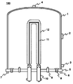
- FIG. 1 is a schematic sectional view showing an example of the configuration of a reaction furnace 100 for producing polycrystalline silicon according to the present invention.
- the reactor 100 is an apparatus for obtaining a polycrystalline silicon rod 12 by vapor-depositing polycrystalline silicon on the surface of the silicon core wire 11 by the Siemens method, and is composed of a base plate 5 and a bell jar 1.
- the base plate 5 is provided with a metal electrode 10 for supplying a current to the silicon core wire 11, a gas nozzle 9 for supplying a process gas such as nitrogen gas, hydrogen gas, trichlorosilane gas, and an exhaust port 8 for exhausting the exhaust gas.
- the base plate 5 has a refrigerant inlet 6 and an outlet 7 for cooling itself.
- the bell jar 1 has a refrigerant inlet part 3 and an outlet part 4 for cooling itself, and further has a viewing window 2 for visually confirming the inside from the outside.
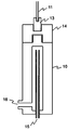
- FIG. 2 is a diagram for explaining an example of an arrangement relationship among the electrode 10, the adapter 14, the core wire holder 13, and the silicon core wire 11 when a heat insulating sheet to be described later is not arranged.
- the metal electrode 10 has a refrigerant inlet 15 and an outlet 16 for cooling itself, and has a structure on which an adapter 14 can be placed.
- the core wire holder 13 is fixed to the upper part of the adapter 14, and the silicon core wire 11 is fixed to the core wire holder 13.
- the adapter 14 and the core wire holder 13 do not need to be provided as separate members, and may be an integrated core wire holder in which the adapter 14 and the core wire holder 13 are a single member.
- the electrode 10, the adapter 14, the core wire holder 13, and the silicon core wire 11 are required to have a contact area necessary for energization. Moreover, it is necessary to have sufficient strength to hold the polycrystalline silicon rod obtained by the polycrystalline silicon precipitation reaction.
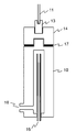
- FIG. 3 is a diagram for explaining an example of an arrangement relationship of the electrode 10, the adapter 14, the core wire holder 13, and the silicon core wire 11 when a heat insulating sheet is arranged.
- the polycrystalline silicon manufacturing apparatus of the present invention includes at least a carbon core wire holder 13 that holds the silicon core wire 11 and an electrode 10 for energizing the silicon core wire 11, and reaches from the electrode 10 to the silicon core wire 11.
- a heat insulating sheet 17 is disposed in at least one part of the conductive path. The heat conductivity in the thickness direction of the heat insulating sheet 17 is lower than the heat conductivity of the core wire holder 13.
- the heat insulating sheet 17 is provided at the contact portion between the adapter 14 and the electrode 10.
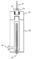
- FIGS. 4 to 6 an embodiment (FIG. 4) in which a heat insulating sheet 17 is disposed at the contact portion between the core wire holder 13 and the adapter 14, the silicon core wire 11 and the core wire holder 13
- positioned at the part may be sufficient.
- the heat insulating sheet 17 may be disposed in at least one of a contact portion between the silicon core wire 11 and the core wire holder 13, a contact portion between the core wire holder 13 and the adapter 14, and a contact portion between the adapter 14 and the electrode 10.
- the sheet is made of a material having a degree of conductivity necessary for heating the silicon core wire, and is more thermally conductive than the carbon material that is a constituent material of the core wire holder 13 and the adapter 14. If the property is low, it is effective to use this as a heat insulating sheet. That is, by using such a heat insulating sheet 17, heat radiation to the cooled electrode 10 when the silicon core wire 11 is heated is suppressed, while initial heating of the silicon core wire 11 is also efficiently performed. .
- the heat insulating property and the electrical conductivity of the heat insulating sheet 17 are basically a trade-off.
- the thermal conductivity in the thickness direction of the sheet is preferably 10 W / mK or less at 25 ° C., more preferably 5 W / mK or less.
- the electrical resistivity in the thickness direction is preferably 5000 ⁇ ⁇ m or less, more preferably 2000 ⁇ ⁇ m or less at 25 ° C.
- the preferable thickness of a heat insulation sheet is 0.1 mm or more and 4.0 mm or less, More preferably, it is 0.2 mm or more and 1.0 mm or less. When the heat insulating sheet is too thick, it causes unnecessary energy loss, and when it is too thin, the heat blocking effect may not be sufficiently obtained.
- the heat insulating sheet 17 is not particularly limited as long as it has a heat conductivity and conductivity as described above, and is a heat resistant material, and a preferable material is a carbon sheet obtained by rolling graphite. Specifically, carbon sheets obtained by heating and rolling acid-treated graphite (for example, those described in JP-A-58-128807 (Patent Document 3) and JP-A-2006-62922 (Patent Document 4)). Etc.). Since such a material has high conductivity in the area direction, it is easy to ensure sufficient conductivity while obtaining a heat insulating effect. In addition, the carbon sheet of such a physical characteristic is marketed, and can be obtained easily.
- the silicon core wire 11 is energized from the electrode 10 to deposit polycrystalline silicon on the surface of the silicon core wire 11 heated to a predetermined temperature.
- the silicon core wire 11 is heated to a temperature at which the silicon core wire 11 can be energized by heating the silicon core wire 11 using an external heater (not shown), and when the temperature of the silicon core wire 11 reaches 200 to 400 ° C. 11 is applied with a voltage from the electrode 10, and the temperature of the silicon core wire 11 is set to 900 to 1300 ° C.
- a mixed gas of trichlorosilane and hydrogen, which is a raw material, is introduced from the raw material nozzle 9 to deposit polycrystalline silicon on the silicon core wire 11, and the reaction is stopped when the polycrystalline silicon has grown to a predetermined size.
- the heating time of the silicon core wire 11 can be greatly shortened.
- it is possible to start energization with a relatively low energization start voltage in a limited heating time it is possible to suppress discharge between the silicon core wire 11 and the core wire holder 13 and the like. It is possible to prevent the core wire from falling down.
- Examples A and B Polycrystalline silicon was grown under the following conditions. First, four silicon core wires of 8 mm square and 1500 mm length were installed in the reaction furnace, the inside of the furnace was in a hydrogen atmosphere, and initial heating was performed for 10 minutes with a carbon heater (110 kW, heater surface temperature 1250 ° C.). Next, the voltage applied to the silicon core wire was gradually increased, the voltage when the current value began to increase was taken as the energization start voltage, and the voltage was adjusted so that a current of 10 A would flow after energization. After 15 minutes from the start of energization, the silicon core wire was taken out, and the depth of scratches generated on the silicon core wire was measured with a surface roughness measuring instrument.
- Example A A carbon sheet having a thickness of 1 mm and a thermal conductivity of 5 W / mK in the thickness direction was disposed between the electrode and the adapter.
- Example B A carbon heat insulating sheet having a thickness of 1 mm and a thermal conductivity of 5 W / mK in the thickness direction is disposed between the electrode and the adapter, and 0.2 mm thick heat is further interposed between the core wire holder and the silicon core wire.
- a carbon sheet having a conductivity of 5 W / mK was disposed.
- Comparative example a A heat insulating sheet is not installed between the electrode, the adapter, the core wire holder, and the silicon core wire.
- Examples C and D Two series of silicon core wires of 8 mm square and 1500 mm length were installed in the reactor (total of 8 wires), and under the same conditions as in Examples A and B, initial heating was performed with a carbon heater, and energization was started. Then, silicon deposition reaction was carried out by introducing trichlorosilane and hydrogen gas.
- Example C A carbon sheet having a thickness of 1 mm and a thermal conductivity of 5 W / mK in the thickness direction was disposed between the electrode and the adapter.
- Example D A carbon heat insulating sheet having a thickness of 1 mm and a thermal conductivity of 5 W / mK in the thickness direction is disposed between the electrode and the adapter, and 0.4 mm thick heat is further interposed between the core wire holder and the silicon core wire.
- a carbon sheet having a conductivity of 5 W / mK was disposed.
- Comparative example b A heat insulating sheet is not installed between the electrode, the adapter, the core wire holder, and the silicon core wire.
- the present invention suppresses the degree to which the heat of the silicon core wire heated by the carbon heater is dissipated to the electrode side, thereby efficiently increasing the temperature of the silicon core wire at the start of the precipitation reaction (at the start of energization). I will provide a.
Landscapes
- Chemical & Material Sciences (AREA)
- Organic Chemistry (AREA)
- Inorganic Chemistry (AREA)
- Silicon Compounds (AREA)
Abstract
本発明の多結晶シリコン製造装置は、少なくとも、シリコン芯線11を保持する炭素製の芯線ホルダ13と、シリコン芯線11に通電するための電極10とを備えており、電極10からシリコン芯線11に至る導電経路の少なくとも一か所に断熱シート17が配置されている。そして、この断熱シート17の厚み方向の熱伝導度は芯線ホルダ13の熱伝導度よりも低いものとされる。これにより、カーボンヒータにより加熱されたシリコン芯線11の熱が電極10側へと放熱される程度が抑制され、析出反応開始時通電開始時においてシリコン芯線11の温度を効率よく高めることができる。
Description
本発明は、多結晶シリコンの製造技術に関する。
半導体用単結晶シリコンあるいは太陽電池用シリコンの原料となる多結晶シリコンの製造方法として、シーメンス法が知られている。シーメンス法は、クロロシランを含む原料ガスを加熱されたシリコン芯線に接触させることにより、該シリコン芯線の表面に多結晶シリコンをCVD(Chemical Vapor Deposition)法を用いて気相成長させる方法である。
シーメンス法により多結晶シリコンを気相成長する際の反応炉は、ベルジャーと呼ばれる上部構造体とベースプレートと呼ばれる下部構造体(底板)により構成される空間内にシリコン芯線を鉛直方向2本、水平方向1本の鳥居型に組み立て、該鳥居型のシリコン芯線の両端を一対のカーボン製の芯線ホルダを介してベースプレート上に配置した一対の金属製の電極に固定する。この構成は、例えば特公昭37-18861号公報(特許文献1)に開示されている。
電極は、絶縁物を挟んでベースプレートを貫通し、配線を通して別の電極に接続されるか、反応炉外に配置された電源に接続される。気相成長中に多結晶シリコンが析出することを防止するために、電極とベースプレートとベルジャーは水などの冷媒を用いて冷却される。電極と芯線ホルダは直接接合してもかまわないが、電極の損傷を防止目的から、電極と芯線ホルダの間にカーボン製のアダプタを設ける。
電極から電流を導通させてシリコン芯線を水素雰囲気中で900℃以上1200℃以下の温度範囲に加熱しながら、原料ガスとして例えばトリクロロシランと水素の混合ガスをガスノズルから反応炉内に供給すると、シリコン芯線上にシリコンが気相成長し、所望の直径の多結晶シリコン棒が逆U字状に形成される。
ところで、シリコン芯線は多結晶又は単結晶のシリコンで作製されるが、高純度多結晶シリコン製造のために用いられるシリコン芯線は不純物濃度の低い高純度なものである必要があり、具体的には、比抵抗が500Ω・cm程度以上の高抵抗のものであることが求められる。このような高抵抗のシリコン芯線の通電は、一般に常温では開始できないため、予めシリコン芯線を200~400℃程度に初期加熱して比抵抗を下げて(導電性を高めて)から通電する必要がある。
このような初期加熱のために、反応炉の中央または内周面に初期加熱用のカーボンヒータを設けておき、反応開始時には、先ずこのカーボンヒータを通電により発熱させ、その際に発生する輻射熱によってカーボンヒータ周辺に配置されているシリコン芯線を所望の温度にまで加熱する。そして、かかる加熱によりシリコン芯線の温度が200℃~400℃に達すれば、長さ当たり2.0V/cm~8.0V/cmの電圧をシリコン芯線に印加することにより、シリコン芯線の表面温度を900℃以上1300℃以下の範囲に加熱する通電の開始が可能となる。
一旦シリコン芯線への通電が開始されれば、その後はカーボンヒータを用いた加熱を利用しなくとも、シリコン芯線自身の発熱により表面温度が維持されるため析出反応は持続的に進行する。そのため、上述のシリコン芯線への通電開始後は、カーボンヒータの電源はOFFされる。
ところで、析出反応開始時(通電開始時)の初期加熱によりシリコン芯線が充分な温度に達しないと、シリコン芯線の比抵抗は十分には低下しない。このため、通電開始時の印加電圧は高めに設定する必要があるが、印加電圧を高くすると、芯線ホルダとシリコン芯線との間で火花放電が発生し易くなり、シリコン芯線にダメージを与えてしまう。このようなダメージは、析出反応中にシリコン芯線が倒壊するなどの原因ともなる。
すなわち、多結晶シリコンの安定的生産の観点からは、析出反応開始時(通電開始時)において、放電等が生じない条件下でシリコン芯線を充分な温度にまで高めることが求められる。そのための方法のひとつとして、ヒータの能力をアップさせたり赤外線照射によりシリコン芯線を加熱するといった選択もある(例えば、特開2001-278611号公報(特許文献2等を参照)。しかし、この場合には、加熱設備等のコストと運転費がアップせざるを得ない。
初期加熱時においてシリコン芯線の温度を効率よく上げるためには、シリコン芯線からの放熱を抑えることが重要である。シリコン芯線はカーボンヒータからの輻射熱により温められるが、シリコン芯線からは、周囲のガスへの対流伝熱や冷却された電極への伝導伝熱により放熱される。
伝導伝熱による放熱を低減させるためには、芯線ホルダとアダプタの材質を熱伝導度の低いものとすればよい。しかし、これらの部材には、耐熱性や含有不純物量あるいはコストなどの観点からカーボンが使用されることが多く、カーボンの熱伝導度は80~180W/mKと比較的高い。また、芯線ホルダやアダプタを長尺化して電極との距離を大きく取るという選択もあるが、この場合には、カーボン部材費のアップや反応炉内空間を大きくしなければならないといった問題がある。
本発明は、かかる課題を解決するためになされたものであり、カーボンヒータにより加熱されたシリコン芯線の熱が電極側へと放熱される程度を抑制し、これにより、析出反応開始時(通電開始時)において、シリコン芯線の温度を効率よく高める技術を提供することにある。
上述の課題を解決するために、本発明に係る第1の態様の多結晶シリコンの製造装置は、反応炉内で加熱されたシリコン芯線に原料ガスを供給することにより前記シリコン芯線の表面に多結晶シリコンを析出させるための多結晶シリコン製造装置であって、前記シリコン芯線を保持する炭素製の芯線ホルダと、前記シリコン芯線に通電するための電極とを備え、前記電極から前記シリコン芯線に至る導電経路の少なくとも一か所に断熱シートが配置されており、前記断熱シートの厚み方向の熱伝導度が前記芯線ホルダの熱伝導度よりも低いことを特徴とする。
また、本発明に係る第2の態様の多結晶シリコンの製造装置は、反応炉内で加熱されたシリコン芯線に原料ガスを供給することにより前記シリコン芯線の表面に多結晶シリコンを析出させるための多結晶シリコン製造装置であって、前記シリコン芯線を保持する炭素製の芯線ホルダと、前記シリコン芯線に通電するための電極とを備え、前記シリコン芯線と前記芯線ホルダとの接触部に断熱シートが配置されており、前記断熱シートの厚み方向の熱伝導度が前記芯線ホルダの熱伝導度よりも低いことを特徴とする。
さらに、本発明に係る第3の態様の多結晶シリコンの製造装置は、反応炉内で加熱されたシリコン芯線に原料ガスを供給することにより前記シリコン芯線の表面に多結晶シリコンを析出させるための多結晶シリコン製造装置であって、前記シリコン芯線を保持する炭素製の芯線ホルダと、前記シリコン芯線に通電するための電極と、前記芯線ホルダを前記電極に載置するための炭素製のアダプタとを備え、前記シリコン芯線と前記芯線ホルダとの接触部、前記芯線ホルダと前記アダプタとの接触部、および前記アダプタと前記電極との接触部の少なくともひとつに断熱シートが配置されており、前記断熱シートの厚み方向の熱伝導度が前記芯線ホルダおよび前記アダプタの熱伝導度よりも低いことを特徴とする。
好ましくは、前記断熱シートの厚み方向の熱伝導度は、25℃において、10W/mK以下であり、より好ましくは、5W/mK以下である。
また、好ましくは、前記断熱シートの厚み方向の電気抵抗率は、25℃において、5000μΩ・m以下であり、より好ましくは、2000μΩ・m以下である。
さらに、好ましくは、前記断熱シートの厚みは、0.1mm以上4.0mm以下であり、より好ましくは、0.2mm以上1.0mm以下である。
本発明に係る多結晶シリコンの製造方法は、本発明の多結晶シリコン製造装置を用い、前記電極から前記シリコン芯線に通電し、所定温度に加熱された前記シリコン芯線の表面に多結晶シリコンを析出させることを特徴とする。
本発明は、厚み方向の熱伝導度が芯線ホルダの熱伝導度よりも低い断熱シートを、電極からシリコン芯線に至る導電経路の少なくとも一か所に配置することとしたので、カーボンヒータにより加熱されたシリコン芯線の熱が電極側へと放熱される程度が抑制され、これにより、析出反応開始時(通電開始時)において、シリコン芯線の温度を効率よく高める技術が提供される。
以下に、図面を参照して、本発明を実施するための形態について説明する。なお、以下では、原料ガスとしてトリクロロシランを用いるシーメンス法を例に説明するが、モノシランやジクロロシランなどの他の原料ガスとして用いることもできることは言うまでもない。
図1は、本発明の多結晶シリコン製造のための反応炉100の構成の一例を示す概略断面図である。反応炉100は、シーメンス法によりシリコン芯線11の表面に多結晶シリコンを気相成長させて多結晶シリコン棒12を得るための装置であり、ベースプレート5とベルジャー1により構成される。
ベースプレート5には、シリコン芯線11に電流を供給する金属電極10と、窒素ガス、水素ガス、トリクロロシランガスなどのプロセスガスを供給するガスノズル9と、排気ガスを排出する排気口8が配置されている。また、ベースプレート5には、自身を冷却するための冷媒の入口部6と出口部7を有している。
ベルジャー1は、自身を冷却するための冷媒の入口部3と出口部4を有し、さらに、外部から内部を目視確認するためののぞき窓2を有している。
図2は、後述する断熱シートを配置しない場合の、電極10、アダプタ14、芯線ホルダ13、およびシリコン芯線11の配置関係の一例を説明するための図である。金属製の電極10は、自身を冷却するための冷媒の入口15と出口16を有しており、上部にはアダプタ14を載置できる構造になっている。アダプタ14の上部には芯線ホルダ13が固定され、さらに、芯線ホルダ13にはシリコン芯線11が固定される。なお、アダプタ14と芯線ホルダ13は別の部材として設ける必要はなく、アダプタ14と芯線ホルダ13が単一の部材としてある、一体型の芯線ホルダとしてもよい。
電極10、アダプタ14、芯線ホルダ13、およびシリコン芯線11は、通電のために必要な接触面積を有することが必要とされる。また、多結晶シリコンの析出反応により得られる多結晶シリコン棒を保持するための十分な強度を有することが必要である。
図3は、断熱シートを配置した場合の、電極10、アダプタ14、芯線ホルダ13、およびシリコン芯線11の配置関係の一例を説明するための図である。
本発明の多結晶シリコン製造装置は、少なくとも、シリコン芯線11を保持する炭素製の芯線ホルダ13と、シリコン芯線11に通電するための電極10とを備えており、電極10からシリコン芯線11に至る導電経路の少なくとも一か所に断熱シート17が配置されている。そして、この断熱シート17の厚み方向の熱伝導度は芯線ホルダ13の熱伝導度よりも低いものとされる。
図3に示した例では、断熱シート17は、アダプタ14と電極10との接触部に設けられている。
このような態様のほか、図4~6に図示したように、芯線ホルダ13とアダプタ14との接触部に断熱シート17が配置されている態様(図4)、シリコン芯線11と芯線ホルダ13との接触部に断熱シート17が配置されている態様(図5)、シリコン芯線11と芯線ホルダ13との接触部、芯線ホルダ13とアダプタ14との接触部、およびアダプタ14と電極10との接触部に断熱シート17が配置されている態様(図6)などであってもよい。
要するに、シリコン芯線を保持する炭素製の芯線ホルダ13と、シリコン芯線13に通電するための電極10と、芯線ホルダ13を電極10に載置するための炭素製のアダプタ14を備えている場合において、シリコン芯線11と芯線ホルダ13との接触部、芯線ホルダ13とアダプタ14との接触部、およびアダプタ14と電極10との接触部の少なくともひとつに断熱シート17が配置されていればよい。
熱伝導性の低い材料は、一般に導電性が低い。このため、シリコン芯線11と電極10のに至る導電経路に熱伝導性の低い材料を介入させることはこれまで想定されてこなかった。しかし、本発明者らの知見によれば、シリコン芯線の加熱に必要な程度の導電性を有する材料から成るシートであって、芯線ホルダ13とアダプタ14の構成材料である炭素材よりも熱伝導性が低いものであれば、これを断熱シートとして使用することは有効である。つまり、このような断熱シート17を用いることで、シリコン芯線11を加熱した際の、冷却されている電極10への放熱は抑制される一方で、シリコン芯線11の初期加熱も効率的に行われる。
断熱シート17の断熱性と導電性は基本的にはトレードオフになるが、シートの厚さ方向の熱伝導度として、25℃において、10W/mK以下の値をもつものが好ましく、より好ましくは5W/mK以下である。また、通電に必要な導電性を確保する観点から、厚さ方向の電気抵抗率が、25℃において、5000μΩ・m以下であることが好ましく、より好ましくは2000μΩ・m以下である。さらに、断熱シートの好ましい厚さは、0.1mm以上4.0mm以下であり、より好ましくは0.2mm以上1.0mm以下である。断熱シートが厚すぎる場合には不要なエネルギロスの原因になり、薄すぎる場合には熱の遮断効果が十分に得られない場合がある。
断熱シート17は、上述したような熱伝導性と導電性を有し、熱耐性がある材料であれば特に限定されないが、好ましい材料としてはグラファイトを圧延した炭素シートを挙げることができる。具体的には、酸処理黒鉛を加熱膨張させ圧延した炭素シート(例えば、特開昭58-128807号公報(特許文献3)や特開2006-62922号公報(特許文献4)に記載されたもの等)を挙げることができる。このような材料は、面積方向には高い導電性をもつため、断熱効果を得つつ充分な導電性を確保し易い。なお、このような物理特性の炭素シートは市販されており、容易に入手可能である。
本発明に係る多結晶シリコンの製造方法では、上述した多結晶シリコン製造装置を用い、電極10からシリコン芯線11に通電し、所定温度に加熱されたシリコン芯線11の表面に多結晶シリコンを析出させる。
すなわち、外部ヒータ(不図示)を用いてシリコン芯線11を加熱して通電可能な温度までシリコン芯線11の温度を上昇させ、シリコン芯線11の温度が200~400℃となった段階で、シリコン芯線11に電極10より電圧を印加して通電させてシリコン芯線11の温度を900~1300℃とする。そこに原料であるトリクロロシランと水素の混合ガスを原料ノズル9より導入し、シリコン芯線11上に多結晶シリコンを析出させ、所定の大きさまで多結晶シリコンが成長した段階で反応を停止する。
本発明に係る多結晶シリコンの製造装置を用いた場合には、シリコン芯線11の加熱時間を大幅に短縮することができる。また、限られた加熱時間において、比較的低い通電開始電圧での通電開始が可能であることから、シリコン芯線11と芯線ホルダ13の間等での放電を抑制することができ、多結晶シリコン成長中での芯線の倒れを防止することができる。
[実施例AおよびB]
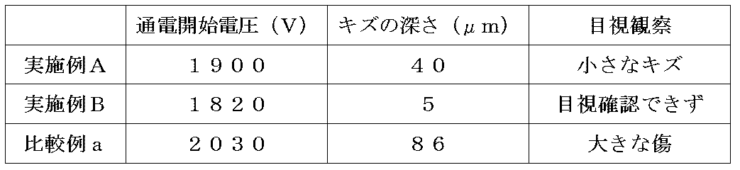
下記の条件で多結晶シリコンの成長を行った。先ず、反応炉に8mm角で1500mm長のシリコン芯線4本を設置して、炉内を水素雰囲気とし、カーボンヒータ(110KW、ヒータ表面温度1250℃)により10分間の初期加熱を行った。次に、シリコン芯線に印加する電圧を徐々に上げていき、電流値が上昇し始めたときの電圧を通電開始電圧とし、通電後は10Aの電流が流れるように電圧を調整した。通電開始より15分後に停止して、シリコン芯線を取り出し、シリコン芯線に発生したキズの深さを表面粗さ測定器により測定した。
下記の条件で多結晶シリコンの成長を行った。先ず、反応炉に8mm角で1500mm長のシリコン芯線4本を設置して、炉内を水素雰囲気とし、カーボンヒータ(110KW、ヒータ表面温度1250℃)により10分間の初期加熱を行った。次に、シリコン芯線に印加する電圧を徐々に上げていき、電流値が上昇し始めたときの電圧を通電開始電圧とし、通電後は10Aの電流が流れるように電圧を調整した。通電開始より15分後に停止して、シリコン芯線を取り出し、シリコン芯線に発生したキズの深さを表面粗さ測定器により測定した。
具体的な装置の条件は以下の通りである。
実施例A:電極とアダプタの間に厚さ1mmの、厚さ方向の熱伝導度5W/mKのカーボンシートを配置した。
実施例B:電極とアダプタの間に厚さ1mmの、厚さ方向の熱伝導度5W/mKのカーボン断熱シートを配置し、さらに、芯線ホルダとシリコン芯線の間に0.2mm厚さの熱伝導度5W/mKのカーボンシートを配置した。
比較例a:電極、アダプタ、芯線ホルダ、シリコン芯線のすべての間に断熱シートを設置しない。
実施例A:電極とアダプタの間に厚さ1mmの、厚さ方向の熱伝導度5W/mKのカーボンシートを配置した。
実施例B:電極とアダプタの間に厚さ1mmの、厚さ方向の熱伝導度5W/mKのカーボン断熱シートを配置し、さらに、芯線ホルダとシリコン芯線の間に0.2mm厚さの熱伝導度5W/mKのカーボンシートを配置した。
比較例a:電極、アダプタ、芯線ホルダ、シリコン芯線のすべての間に断熱シートを設置しない。
結果を表1に纏めた。この結果より、断熱シートを多く設置した方が、シリコン芯線に発生する火花放電跡と推測されるキズの深さが小さくなる。
[実施例CおよびD]
反応炉に8mm角で1500mm長のシリコン芯線4本を2系列(計8本)を設置して、実施例AおよびBと同様の条件により、カーボンヒータにて初期加熱を行い通電開始し、その後、トリクロロシランと水素ガスを導入しシリコンの析出反応を行った。
反応炉に8mm角で1500mm長のシリコン芯線4本を2系列(計8本)を設置して、実施例AおよびBと同様の条件により、カーボンヒータにて初期加熱を行い通電開始し、その後、トリクロロシランと水素ガスを導入しシリコンの析出反応を行った。
具体的な装置の条件は以下の通りである。
実施例C:電極とアダプタの間に厚さ1mmの、厚さ方向の熱伝導度5W/mKのカーボンシートを配置した。
実施例D:電極とアダプタの間に厚さ1mmの、厚さ方向の熱伝導度5W/mKのカーボン断熱シートを配置し、さらに、芯線ホルダとシリコン芯線の間に0.4mm厚さの熱伝導度5W/mKのカーボンシートを配置した。
比較例b:電極、アダプタ、芯線ホルダ、シリコン芯線のすべての間に断熱シートを設置しない。
実施例C:電極とアダプタの間に厚さ1mmの、厚さ方向の熱伝導度5W/mKのカーボンシートを配置した。
実施例D:電極とアダプタの間に厚さ1mmの、厚さ方向の熱伝導度5W/mKのカーボン断熱シートを配置し、さらに、芯線ホルダとシリコン芯線の間に0.4mm厚さの熱伝導度5W/mKのカーボンシートを配置した。
比較例b:電極、アダプタ、芯線ホルダ、シリコン芯線のすべての間に断熱シートを設置しない。
結果を表2に纏めた。比較例bではシリコン棒直径20mmφにて倒壊が生じたのに対し、実施例CおよびDの何れにおいても、シリコン棒の倒壊は起きなかった。

本発明は、カーボンヒータにより加熱されたシリコン芯線の熱が電極側へと放熱される程度を抑制し、これにより、析出反応開始時(通電開始時)において、シリコン芯線の温度を効率よく高める技術を提供する。
1 ベルジャー
2 のぞき窓
3 冷媒入口部
4 冷媒出口部
5 ベースプレート
6 冷媒入口部
7 冷媒出口部
8 反応排ガス出口
9 原料ガス供給ノズル
10 電極
11 シリコン芯線
12 多結晶シリコン棒
13 芯線ホルダ
14 アダプタ
15 冷媒入口部
16 冷媒出口部
17 断熱シート
100 反応炉
2 のぞき窓
3 冷媒入口部
4 冷媒出口部
5 ベースプレート
6 冷媒入口部
7 冷媒出口部
8 反応排ガス出口
9 原料ガス供給ノズル
10 電極
11 シリコン芯線
12 多結晶シリコン棒
13 芯線ホルダ
14 アダプタ
15 冷媒入口部
16 冷媒出口部
17 断熱シート
100 反応炉
Claims (10)
- 反応炉内で加熱されたシリコン芯線に原料ガスを供給することにより前記シリコン芯線の表面に多結晶シリコンを析出させるための多結晶シリコン製造装置であって、
前記シリコン芯線を保持する炭素製の芯線ホルダと、前記シリコン芯線に通電するための電極とを備え、
前記電極から前記シリコン芯線に至る導電経路の少なくとも一か所に断熱シートが配置されており、
前記断熱シートの厚み方向の熱伝導度が前記芯線ホルダの熱伝導度よりも低い、ことを特徴とする多結晶シリコン製造装置。 - 反応炉内で加熱されたシリコン芯線に原料ガスを供給することにより前記シリコン芯線の表面に多結晶シリコンを析出させるための多結晶シリコン製造装置であって、
前記シリコン芯線を保持する炭素製の芯線ホルダと、前記シリコン芯線に通電するための電極とを備え、
前記シリコン芯線と前記芯線ホルダとの接触部に断熱シートが配置されており、
前記断熱シートの厚み方向の熱伝導度が前記芯線ホルダの熱伝導度よりも低い、ことを特徴とする多結晶シリコン製造装置。 - 反応炉内で加熱されたシリコン芯線に原料ガスを供給することにより前記シリコン芯線の表面に多結晶シリコンを析出させるための多結晶シリコン製造装置であって、
前記シリコン芯線を保持する炭素製の芯線ホルダと、前記シリコン芯線に通電するための電極と、前記芯線ホルダを前記電極に載置するための炭素製のアダプタとを備え、
前記シリコン芯線と前記芯線ホルダとの接触部、前記芯線ホルダと前記アダプタとの接触部、および前記アダプタと前記電極との接触部の少なくともひとつに断熱シートが配置されており、
前記断熱シートの厚み方向の熱伝導度が前記芯線ホルダおよび前記アダプタの熱伝導度よりも低い、ことを特徴とする多結晶シリコン製造装置。 - 前記断熱シートの厚み方向の熱伝導度は、25℃において、10W/mK以下である、請求項1乃至3の何れか1項に記載の多結晶シリコン製造装置。
- 前記断熱シートの厚み方向の熱伝導度は、25℃において、5W/mK以下である、請求項4に記載の多結晶シリコン製造装置。
- 前記断熱シートの厚み方向の電気抵抗率は、25℃において、5000μΩ・m以下である、請求項1乃至3の何れか1項に記載の多結晶シリコン製造装置。
- 前記断熱シートの厚み方向の電気抵抗率は、25℃において、2000μΩ・m以下である、請求項6に記載の多結晶シリコン製造装置。
- 前記断熱シートの厚みは、0.1mm以上4.0mm以下である、請求項1乃至3の何れか1項に記載の多結晶シリコン製造装置。
- 前記断熱シートの厚みは、0.2mm以上1.0mm以下である、請求項8に記載の多結晶シリコン製造装置。
- 請求項1乃至3の何れか1項に記載の多結晶シリコン製造装置を用い、前記電極から前記シリコン芯線に通電し、所定温度に加熱された前記シリコン芯線の表面に多結晶シリコンを析出させる、ことを特徴とする多結晶シリコンの製造方法。
Applications Claiming Priority (2)
| Application Number | Priority Date | Filing Date | Title |
|---|---|---|---|
| JP2011098983A JP5653830B2 (ja) | 2011-04-27 | 2011-04-27 | 多結晶シリコン製造装置および多結晶シリコン製造方法 |
| JP2011-098983 | 2011-04-27 |
Publications (1)
| Publication Number | Publication Date |
|---|---|
| WO2012147300A1 true WO2012147300A1 (ja) | 2012-11-01 |
Family
ID=47071833
Family Applications (1)
| Application Number | Title | Priority Date | Filing Date |
|---|---|---|---|
| PCT/JP2012/002619 Ceased WO2012147300A1 (ja) | 2011-04-27 | 2012-04-16 | 多結晶シリコン製造装置および多結晶シリコンの製造方法 |
Country Status (2)
| Country | Link |
|---|---|
| JP (1) | JP5653830B2 (ja) |
| WO (1) | WO2012147300A1 (ja) |
Cited By (5)
| Publication number | Priority date | Publication date | Assignee | Title |
|---|---|---|---|---|
| JP2013018675A (ja) * | 2011-07-11 | 2013-01-31 | Shin-Etsu Chemical Co Ltd | 多結晶シリコン製造装置 |
| WO2014103939A1 (ja) * | 2012-12-27 | 2014-07-03 | 株式会社トクヤマ | 多結晶シリコンロッドおよびその製造方法 |
| WO2014168116A1 (ja) * | 2013-04-10 | 2014-10-16 | 株式会社トクヤマ | シリコン製造用芯線ホルダ |
| EP2489634A4 (en) * | 2009-10-14 | 2014-12-31 | Shinetsu Chemical Co | CORE YARN SUPPORT FOR THE PRODUCTION OF POLYCRYSTALLINE SILICON AND METHOD FOR PRODUCING POLYCRYSTALLINE SILICON |
| CN112299421A (zh) * | 2019-07-25 | 2021-02-02 | 信越化学工业株式会社 | 多晶硅制造装置 |
Families Citing this family (2)
| Publication number | Priority date | Publication date | Assignee | Title |
|---|---|---|---|---|
| JP6513842B2 (ja) * | 2018-02-02 | 2019-05-15 | 信越化学工業株式会社 | 多結晶シリコン棒製造用のシリコン芯線および多結晶シリコン棒の製造装置 |
| JP7100192B2 (ja) * | 2018-07-27 | 2022-07-12 | ワッカー ケミー アクチエンゲゼルシャフト | 多結晶シリコン堆積用電極 |
Citations (4)
| Publication number | Priority date | Publication date | Assignee | Title |
|---|---|---|---|---|
| JP2006016243A (ja) * | 2004-07-01 | 2006-01-19 | Sumitomo Titanium Corp | 多結晶シリコン製造方法およびシード保持電極 |
| JP2006240934A (ja) * | 2005-03-04 | 2006-09-14 | Tokuyama Corp | 多結晶シリコンの製造装置 |
| WO2011045881A1 (ja) * | 2009-10-14 | 2011-04-21 | 信越化学工業株式会社 | 多結晶シリコン製造用芯線ホルダおよび多結晶シリコンの製造方法 |
| JP2011195439A (ja) * | 2010-03-19 | 2011-10-06 | Wacker Chemie Ag | 黒鉛電極 |
-
2011
- 2011-04-27 JP JP2011098983A patent/JP5653830B2/ja active Active
-
2012
- 2012-04-16 WO PCT/JP2012/002619 patent/WO2012147300A1/ja not_active Ceased
Patent Citations (4)
| Publication number | Priority date | Publication date | Assignee | Title |
|---|---|---|---|---|
| JP2006016243A (ja) * | 2004-07-01 | 2006-01-19 | Sumitomo Titanium Corp | 多結晶シリコン製造方法およびシード保持電極 |
| JP2006240934A (ja) * | 2005-03-04 | 2006-09-14 | Tokuyama Corp | 多結晶シリコンの製造装置 |
| WO2011045881A1 (ja) * | 2009-10-14 | 2011-04-21 | 信越化学工業株式会社 | 多結晶シリコン製造用芯線ホルダおよび多結晶シリコンの製造方法 |
| JP2011195439A (ja) * | 2010-03-19 | 2011-10-06 | Wacker Chemie Ag | 黒鉛電極 |
Cited By (6)
| Publication number | Priority date | Publication date | Assignee | Title |
|---|---|---|---|---|
| EP2489634A4 (en) * | 2009-10-14 | 2014-12-31 | Shinetsu Chemical Co | CORE YARN SUPPORT FOR THE PRODUCTION OF POLYCRYSTALLINE SILICON AND METHOD FOR PRODUCING POLYCRYSTALLINE SILICON |
| JP2013018675A (ja) * | 2011-07-11 | 2013-01-31 | Shin-Etsu Chemical Co Ltd | 多結晶シリコン製造装置 |
| WO2014103939A1 (ja) * | 2012-12-27 | 2014-07-03 | 株式会社トクヤマ | 多結晶シリコンロッドおよびその製造方法 |
| JPWO2014103939A1 (ja) * | 2012-12-27 | 2017-01-12 | 株式会社トクヤマ | 多結晶シリコンロッドおよびその製造方法 |
| WO2014168116A1 (ja) * | 2013-04-10 | 2014-10-16 | 株式会社トクヤマ | シリコン製造用芯線ホルダ |
| CN112299421A (zh) * | 2019-07-25 | 2021-02-02 | 信越化学工业株式会社 | 多晶硅制造装置 |
Also Published As
| Publication number | Publication date |
|---|---|
| JP2012229144A (ja) | 2012-11-22 |
| JP5653830B2 (ja) | 2015-01-14 |
Similar Documents
| Publication | Publication Date | Title |
|---|---|---|
| JP5653830B2 (ja) | 多結晶シリコン製造装置および多結晶シリコン製造方法 | |
| EP2108619B1 (en) | Polycrystalline silicon reactor | |
| CN101405437B (zh) | 应用混合芯构件制备高纯硅棒的装置和方法 | |
| JP5194003B2 (ja) | 金属コア手段を使用した高純度多結晶シリコン棒の製造方法 | |
| US20120222619A1 (en) | Carbon electrode and apparatus for manufacturing polycrystalline silicon rod | |
| JP2013018701A (ja) | Cvd反応器の電極保持部を保護するための保護装置 | |
| KR101028416B1 (ko) | 박막 제조 방법 및 박막 제조 장치 | |
| JP2008509070A (ja) | 珪素製造用反応装置及び方法 | |
| JP5539292B2 (ja) | 多結晶シリコンの製造方法 | |
| US11519069B2 (en) | Polycrystalline silicon manufacturing apparatus | |
| CN111286780A (zh) | 晶体生长装置及坩埚 | |
| JP5820917B2 (ja) | 多結晶シリコンの製造方法 | |
| JP5865236B2 (ja) | 多結晶シリコン棒の製造装置および製造方法 | |
| WO2012144161A1 (ja) | シリコン芯線の製造方法 | |
| CN111560650A (zh) | 多晶硅制造装置以及多晶硅 | |
| JP2020132472A (ja) | 多結晶シリコン製造装置 | |
| JP3474406B2 (ja) | シリコン製発熱体及びこれを用いた半導体製造装置 | |
| WO2016002232A1 (ja) | 多結晶シリコン棒製造用のシリコン芯線および多結晶シリコン棒の製造装置 | |
| JP6772753B2 (ja) | 多結晶シリコン反応炉 | |
| JP6513842B2 (ja) | 多結晶シリコン棒製造用のシリコン芯線および多結晶シリコン棒の製造装置 | |
| JP2008244389A (ja) | 真空処理装置、真空処理方法及びプラズマcvd方法 | |
| KR101420338B1 (ko) | 씨브이디 반응장치용 절연 슬리브 및 그 절연 슬리브가 구비된 씨브이디 반응장치 | |
| JP7591987B2 (ja) | 多結晶シリコンロッドの製造装置及び製造方法 | |
| JP4681084B1 (ja) | Cvd処理方法およびその方法を使用するcvd装置 | |
| JP2013193931A (ja) | 多結晶シリコンロッドの製造方法 |
Legal Events
| Date | Code | Title | Description |
|---|---|---|---|
| 121 | Ep: the epo has been informed by wipo that ep was designated in this application |
Ref document number: 12777459 Country of ref document: EP Kind code of ref document: A1 |
|
| NENP | Non-entry into the national phase |
Ref country code: DE |
|
| 122 | Ep: pct application non-entry in european phase |
Ref document number: 12777459 Country of ref document: EP Kind code of ref document: A1 |