WO2012147117A1 - 記録媒体、アドレス検出方法、再生及び記録方法 - Google Patents
記録媒体、アドレス検出方法、再生及び記録方法 Download PDFInfo
- Publication number
- WO2012147117A1 WO2012147117A1 PCT/JP2011/002398 JP2011002398W WO2012147117A1 WO 2012147117 A1 WO2012147117 A1 WO 2012147117A1 JP 2011002398 W JP2011002398 W JP 2011002398W WO 2012147117 A1 WO2012147117 A1 WO 2012147117A1
- Authority
- WO
- WIPO (PCT)
- Prior art keywords
- recording
- address
- layer
- data
- address information
- Prior art date
- Legal status (The legal status is an assumption and is not a legal conclusion. Google has not performed a legal analysis and makes no representation as to the accuracy of the status listed.)
- Ceased
Links
Images





Classifications
-
- G—PHYSICS
- G11—INFORMATION STORAGE
- G11B—INFORMATION STORAGE BASED ON RELATIVE MOVEMENT BETWEEN RECORD CARRIER AND TRANSDUCER
- G11B20/00—Signal processing not specific to the method of recording or reproducing; Circuits therefor
- G11B20/10—Digital recording or reproducing
- G11B20/12—Formatting, e.g. arrangement of data block or words on the record carriers
- G11B20/1217—Formatting, e.g. arrangement of data block or words on the record carriers on discs
-
- G—PHYSICS
- G11—INFORMATION STORAGE
- G11B—INFORMATION STORAGE BASED ON RELATIVE MOVEMENT BETWEEN RECORD CARRIER AND TRANSDUCER
- G11B7/00—Recording or reproducing by optical means, e.g. recording using a thermal beam of optical radiation by modifying optical properties or the physical structure, reproducing using an optical beam at lower power by sensing optical properties; Record carriers therefor
- G11B7/007—Arrangement of the information on the record carrier, e.g. form of tracks, actual track shape, e.g. wobbled, or cross-section, e.g. v-shaped; Sequential information structures, e.g. sectoring or header formats within a track
- G11B7/00745—Sectoring or header formats within a track
-
- G—PHYSICS
- G11—INFORMATION STORAGE
- G11B—INFORMATION STORAGE BASED ON RELATIVE MOVEMENT BETWEEN RECORD CARRIER AND TRANSDUCER
- G11B7/00—Recording or reproducing by optical means, e.g. recording using a thermal beam of optical radiation by modifying optical properties or the physical structure, reproducing using an optical beam at lower power by sensing optical properties; Record carriers therefor
- G11B7/24—Record carriers characterised by shape, structure or physical properties, or by the selection of the material
- G11B7/2407—Tracks or pits; Shape, structure or physical properties thereof
- G11B7/24073—Tracks
- G11B7/24082—Meandering
-
- G—PHYSICS
- G11—INFORMATION STORAGE
- G11B—INFORMATION STORAGE BASED ON RELATIVE MOVEMENT BETWEEN RECORD CARRIER AND TRANSDUCER
- G11B7/00—Recording or reproducing by optical means, e.g. recording using a thermal beam of optical radiation by modifying optical properties or the physical structure, reproducing using an optical beam at lower power by sensing optical properties; Record carriers therefor
- G11B2007/0003—Recording, reproducing or erasing systems characterised by the structure or type of the carrier
- G11B2007/0009—Recording, reproducing or erasing systems characterised by the structure or type of the carrier for carriers having data stored in three dimensions, e.g. volume storage
-
- G—PHYSICS
- G11—INFORMATION STORAGE
- G11B—INFORMATION STORAGE BASED ON RELATIVE MOVEMENT BETWEEN RECORD CARRIER AND TRANSDUCER
- G11B2220/00—Record carriers by type
- G11B2220/20—Disc-shaped record carriers
- G11B2220/23—Disc-shaped record carriers characterised in that the disc has a specific layer structure
- G11B2220/235—Multilayer discs, i.e. multiple recording layers accessed from the same side
-
- G—PHYSICS
- G11—INFORMATION STORAGE
- G11B—INFORMATION STORAGE BASED ON RELATIVE MOVEMENT BETWEEN RECORD CARRIER AND TRANSDUCER
- G11B7/00—Recording or reproducing by optical means, e.g. recording using a thermal beam of optical radiation by modifying optical properties or the physical structure, reproducing using an optical beam at lower power by sensing optical properties; Record carriers therefor
- G11B7/004—Recording, reproducing or erasing methods; Read, write or erase circuits therefor
- G11B7/005—Reproducing
- G11B7/0053—Reproducing non-user data, e.g. wobbled address, prepits, BCA
-
- G—PHYSICS
- G11—INFORMATION STORAGE
- G11B—INFORMATION STORAGE BASED ON RELATIVE MOVEMENT BETWEEN RECORD CARRIER AND TRANSDUCER
- G11B7/00—Recording or reproducing by optical means, e.g. recording using a thermal beam of optical radiation by modifying optical properties or the physical structure, reproducing using an optical beam at lower power by sensing optical properties; Record carriers therefor
- G11B7/24—Record carriers characterised by shape, structure or physical properties, or by the selection of the material
- G11B7/2403—Layers; Shape, structure or physical properties thereof
- G11B7/24035—Recording layers
- G11B7/24038—Multiple laminated recording layers
-
- G—PHYSICS
- G11—INFORMATION STORAGE
- G11B—INFORMATION STORAGE BASED ON RELATIVE MOVEMENT BETWEEN RECORD CARRIER AND TRANSDUCER
- G11B7/00—Recording or reproducing by optical means, e.g. recording using a thermal beam of optical radiation by modifying optical properties or the physical structure, reproducing using an optical beam at lower power by sensing optical properties; Record carriers therefor
- G11B7/24—Record carriers characterised by shape, structure or physical properties, or by the selection of the material
- G11B7/2403—Layers; Shape, structure or physical properties thereof
- G11B7/24047—Substrates
- G11B7/2405—Substrates being also used as track layers of pre-formatted layers
Definitions
- the present invention relates to a recording medium on which an address is recorded, such as an optical disc, an address detection of an optical disc, and a reproducing method and recording method for recording and reproducing data from the recording medium.
- Patent Document 1 an optical recording medium in which a plurality of recording layers and one servo layer are stacked is It is disclosed.
- a flat recording layer without a guide track (groove) is formed, and a servo layer having a guide track is formed thereon.
- various servo signals are generated based on the guide track formed in the servo layer, and the address information formed on the guide track is read to specify the position on the medium.
- An object of the present invention is to provide a recording medium having an address structure that simplifies detection and control in a single layer having address information, and a recording and reproducing method.
- a recording medium having an address structure that can be easily controlled from the inner circumference or from the outer circumference is provided.
- the OTP recording and reproduction scheme can be controlled from a single address structure in one servo layer.
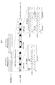
- FIG. 6 shows an ADIP address structure. It is a figure which shows the ADIP address arrangement
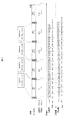
- Part 1 It is a figure which shows the ADIP address arrangement
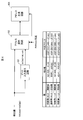
- Part 2) 1 is an optical disc recording and reproducing apparatus according to a first embodiment of the present invention. It is a figure which shows a disc structure.
- FIG. 1 is a block diagram of an address detection circuit according to a first embodiment of the present invention.
- Reference numeral 101 denotes a bit replacement circuit
- 102 denotes an address selection circuit
- 103 denotes an address generation circuit.
- N is a natural number
- the address information is on the groove.
- an ADIP (Address in Pre groove) address structure using wobble as address information will be described as an example.
- an ADIP structure used in DVD + RW will be described as an example using FIG.
- the address by wobble of the DVD + RW contains a signal by the wobble obtained by inverting the phase of the sine wave wobble by 180 ° and the phase modulation of the normal wobble, and forms ADIP address information.
- ADIP Sync Unit including word sync, bit sync and data bit
- ADIP Data Unit including “0” or “1”
- 52 ADIP Units constitute 1 ADIP Word.
- ADIP Word is contained in a proportion of one in four sectors, and one ECC block contains four ADIP addresses. In the address data portion, a total of 51 bits of 22 bits of ADIP address, 8 bits of ADIP auxiliary data, 20 bits of parity, and 1 bit of reserve are stored.
- ADIP addresses are arranged in the same direction as the data recording and reproducing direction, with layer 0 from the inner periphery to the outer periphery and one layer from the outer periphery to the inner periphery.
- the recording and reproduction in the same direction as the ADIP address arrangement direction is equivalent to the conventional one.
- special processing is required in consideration of recording and reproduction in the direction opposite to the ADIP arrangement direction. This will be described using the address detection circuit of FIG. 1 and the ADIP address arrangement configuration and address detection timing diagram of FIG. 3.
- the wobble length of one ADIP Word structure is equal to the data recording length for 4 sectors of data
- the case where the unit recording data length is 16 sectors will be described as an example.
- the ADIP structure in the servo layer is arranged from the inner circumference to the outer circumference, and the even layers (layer 0, layer 2, ...) of the recording layer perform recording and reproduction from the inner circumference to the outer circumference, and the odd layers (recording layer) ..)
- the explanation will be briefly described focusing on the arrangement and detection of the ADIP address of the address data portion.
- ADIP addresses most significant bit A21 and least significant bit A0 are stored per 1 ADIP Word, they are detected in the order of A21, A20, ..., A1, A0 as detection addresses in ADIP Word, The desired ADIP address can be generated by using it as it is.
- recording of the recording / reproducing data having a physical sector number (Physical Sector Number, PSN) 4X in synchronization with the start position of ADIP # (n)
- the playback start position can be identified.
- the detection value as it is is selected by the address selection circuit 102 and is input to the address generation circuit 103 to generate the address [A21, A20,..., A1, A0].
- ADIP Unit information obtained by rearranging ADIP Units also reverses the order of ADIP Units in 1 ADIP Word, and the detection addresses are in the order of A0, A1, ..., A20, A21. As it is detected, address generation is performed by replacing bit positions.
- address detection circuit in FIG. 1 In the address detection circuit in FIG.
- the detected value is replaced by the bit replacement circuit 101 so that the most significant bit of the detection is the least significant bit of the address and the least significant bit of the detection is the most significant bit of the address.
- the address [A21, A20,..., A1, A0] is generated as an input to the address generation circuit 103 by selecting at 103.
- ADIP # by inverting the detection address in the address generation circuit 103
- the address detection circuit is generated by bit replacement or bit inversion. Control can be easily performed by using the address.
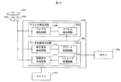
- FIG. 10 shows an example of a recording and reproducing apparatus for recording and reproducing data from an optical disc by using the address configuration and the address detection circuit described in the present embodiment.
- An optical disk 1001, a pickup 1002, a spindle motor 1003, an address reproducing circuit 1004, an address recording circuit 1005, a data recording / reproducing circuit 1005, an external host 1006, and a microcomputer that controls the entire system 1007 are shown.
- As the address generation circuit 1004, a wobble detection circuit 1008 and an address detection circuit 1009 are shown as 1008.
- the address detection circuit 1009 is configured using the circuit described in FIG.
- an RF detection circuit 1010 As the data recording / reproducing circuit 1005, an RF detection circuit 1010, a decoding processing circuit 1011, a recording waveform generation circuit 1012, and an encoding processing circuit 1013 are shown. Further, as a method of recording and reproducing a signal from the optical disc 1001, as shown in FIG. 11, for example, two types of laser beams having different wavelengths are emitted in the optical pickup 1002, and each laser beam passes through the objective lens 1101 By controlling so that a laser spot is generated on the servo layer and the desired recording layer, recording and reproduction of data on the recording layer and reading of a wobble signal from the servo layer become possible.
- the wobble signal read from the servo layer via the pickup from the optical disk 1001 having a single servo layer and a plurality of recording layers in which physical address information is stored is input to the address reproduction circuit 1004 and the address Detect information.
- the wobble detection circuit 1008 performs detection of the wobble signal, generation of a clock synchronized with the wobble, etc., for example, detects ADIP address information embedded in the wobble, and is input to the address detection circuit 1009.
- the address detection and generation are performed by bit replacement and inversion processing according to the reading direction of each layer, and the data recording / reproducing position on the disc is detected.
- recording and reproduction data can be performed by the same processing regardless of the reading direction of each layer as in the prior art.
- encode processing is performed on the data input from the host 1006 by the encoding processing circuit 1013 to generate a recording data sequence, and converted into a recording waveform by the recording waveform generation circuit 1012
- the recording is continuously performed on the recording layer on the optical disc 1001 according to the recording and reproducing direction via the pickup 1002.
- the reproduction waveform read continuously from the recording layer of the optical disc 1001 through the pickup 1002 in the recording and reproduction direction is subjected to waveform processing and binarization processing at the RF detection circuit 1010 to be decoded.
- Decoding is performed in accordance with a predetermined recording format in 1011 and output to the host 1006 as reproduction data.
- the recording and reproduction position can be detected, and the recording and reproduction of data on the recording layer can be performed.
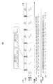
- FIG. 4 is a block diagram of an address detection circuit according to a second embodiment of the present invention. A difference from FIG. 1 is that not the layer information but the address position information is used as a signal for selection switching of the address selection circuit 102. This will be described using the ADIP address arrangement configuration and address detection timing diagrams of FIGS. 4 and 5. As shown in the upper part of FIG.
- Address generation is performed using the address detection circuit of FIG. Even-numbered addresses are detected from the most significant bit, and odd-numbered addresses are detected from the least significant bit. Therefore, in the odd-numbered addresses, the bit replacement circuit 101 performs processing of replacing the bits of the detection value.
- A21, and address generation is performed using the address detection circuit of FIG. 4 as in the case of the even layer. Even in the odd layer, as in the even layer, even-numbered addresses are detected from the most significant bit and odd-numbered addresses are detected from the least significant bit.
- even addresses (0, 2,%) Are detected values as they are, and odd numbers (1, 3,%) Are outputs of bit replacement circuit 101 to generate continuous addresses. It has been explained. However, even if the even-numbered (1, 3,%) Detection addresses are read out and controlled using only the even-numbered (0, 2,%) Detection values, detection is possible similarly. As the even-numbered (0, 2,%) Detection address in the even layers (layer 0, layer 2,%) As in X, X + 2,. If even-numbered detection addresses can be specified based on the position information of ADIP Word as ⁇ X-3, ⁇ X-1, ...
- ADIP Data recording and reproduction can be realized similarly in synchronization with the address.
- the number of bits of ADIP address information that can be stored in one ADIP Word is 22 bits, but the number of bits of ADIP address information that can be stored in one ADIP Word is the number of bits for two layers Even if it is a structure that can store (for 44 bits if it is equivalent to 22 bits), the same control can be performed.
- This will be described using the ADIP address arrangement configuration and the timing chart of the address detection of FIG. As shown in the upper part of FIG.
- ADIP # (n + 1) the first half of each ADIP Word 22 In the bits, the address of the even layer is constructed from the most significant bit, and the address of the odd layer is stored from the least significant bit in the second half 22 bits.
- 22 bits of the first half of the address information of each ADIP word are generated as detection addresses from each layer as they are as detection values, address detection can be easily performed.
- it is possible to double-detect the address from each ADIP Word by replacing the 22 bits in the second half of the address information of each ADIP Word and then performing bit inversion, which makes it possible to further improve detection accuracy. .
- the address detection circuit is generated by bit replacement or bit inversion. Control can be easily performed by using the address.
- the address structure of the medium in the present embodiment by making the bit arrangement method of the desired address symmetrical also from the inner circumferential direction and the outer circumferential direction, the address generation method in each layer can be made common and more easily. You will be able to control.
- the address detection circuit described in FIG. The position where the data is recorded and reproduced is detected, and the recording and reproduction of the data on the recording layer can be performed.
- ADIP address of the odd layer ⁇ X-1 [B21, B20, ..., B1, B0], the address most significant bit A21 of the even layer, the least significant bit B0 of the odd layer, ..., the uppermost of the even layer Based on the rule of storing in order of bit A0 and the most significant bit B21 of the odd layer, it is divided and stored in 2 ADIP words.
- An address of -1 is output in order from the least significant bit, and can be converted into an output from the most significant bit in order from B21, B20, ..., B1, B0 as an output of the bit replacement circuit 101.
- the address detected by the wobble of the servo layer is ADIP # (n + 3) because recording / reproduction is performed from the outer circumference to the inner circumference.
- odd bit selection circuit 702 is A0, A1, ..., A20, A21 and ADIP address
- the detection method can be made common to the even layer and the odd layer.
- the number of bits of ADIP address information that can be stored in one ADIP Word as described in the second embodiment is the number of bits for two layers (44 bits for 22 bits). Even if it is possible structure, it can control similarly. This will be described using the ADIP address arrangement configuration and the timing chart of the address detection of FIG. As shown in the upper part of FIG.
- the address detection circuit is generated by bit replacement or bit inversion. Control can be easily performed by using the address.
- the address structure of the medium in the present embodiment by making the bit arrangement method of the desired address symmetrical also from the inner circumferential direction and the outer circumferential direction, the address generation method in each layer can be made common and more easily. You will be able to control.
- the address detection circuit described in FIG. The position where the data is recorded and reproduced is detected, and the recording and reproduction of the data on the recording layer can be performed.
- ADIP address stored in each ADIP Word has been described in the above embodiments, it goes without saying that other address information stored as address data such as ADIP auxiliary data and a parity portion is also included. Similarly, by performing the arrangement and bit replacement, it becomes possible to cope with reading and detection at the time of recording and reproduction of the even layer and the odd layer.
- the storage method of the address information has been described as storing so that it can be read out sequentially from the most significant bit of the address in the direction of reading, it is not particularly limited to this storage method. As long as the desired address arrangement method can be made symmetrical from the outer peripheral direction, various modifications can be made.
- LPP Land Pre-Pit
- PID Physical ID
- BD Ad-Pit
- the present invention can be applied to various address structures constituting physical address information. Although an address structure having one address information per one unit recording data has been described as an example like the ADIP address structure of DVD + RW, one unit recording data (one) is described as a PID address structure of DVD-RAM.
- the address in each layer is symmetrical by arranging the desired address arrangement and bit arrangement in the inner and outer circumferential directions.
- the detection method can be applied for the purpose of common.
Landscapes
- Engineering & Computer Science (AREA)
- Signal Processing (AREA)
- Optical Recording Or Reproduction (AREA)
- Signal Processing For Digital Recording And Reproducing (AREA)
Abstract
単一のアドレス層と複数の記録層を持つ記録媒体におけるアドレス構造を提供する。 記録層の偶数層(層0、層2、…)のアドレスを最上位ビットよりアドレス層の内周より格納、記録層の奇数層(層1、層3、…)のアドレスを最下位ビットよりアドレス層の内周より交互に格納することで、偶数層の記録再生時に内周より、あるいは奇数層の記録再生時に外周よりアドレス情報を検出でき、検出方法も共通に出来るため、容易に制御が可能となる。
Description
本発明は、アドレスが記録されている記録媒体、例えば光ディスク、光ディスクのアドレス検出、記録媒体よりデータの記録再生を行う再生方法、記録方法に関する。
近年、記録媒体の大容量化に伴い、積層方向に複数の記録層を有する光記録媒体が開発され、特許文献1には、複数の記録層と一つのサーボ層が積層された光記録媒体が開示されている。この記録媒体において、ガイドトラック(グルーブ)のない平坦な記録層が形成され、その上に、ガイドトラックを有するサーボ層が形成される。
記録再生時には、サーボ層に形成されたガイドトラックをもとに各種サーボ信号を生成し、ガイドトラック上に形成されたアドレス情報を読み取ることで、媒体上の位置の特定を行う。
特許文献1で示されるような複数の記録層と一つのサーボ層を有する媒体において、従来の多層光ディスクでも採用されていたような層0に対しては最内周部から外周方向に向けて記録再生を行い、層0の記録再生が終了した後に、層1に対して最外周部から内周方向に向けて記録再生を行う方式(OTP:Opposite Track Path)を採用した場合、一つのサーボ層に最内周から外周へのみ形成されたアドレス情報が内周から読み取りのみを考慮した構成のままだと、アドレス情報の読み取りとアドレス情報と記録層の位置相関を図る上では、検出方法や制御方法が複雑になってしまう。
本発明の目的は、アドレス情報を有する単一の層における、検出及び制御が簡素となるアドレス構造を持つ記録媒体、及び記録再生方法を提供することである。
上記問題を解決するために、内周から、あるいは外周から検出しても容易に制御可能なアドレス構造を有する記録媒体を提供する。
本発明により、一つのサーボ層にある単一のアドレス構造からOTP記録再生方式を制御できる。
以下、図面を参照して本発明の実施例について説明する。
図1は本発明の第1の実施例であるアドレス検出回路の構成図である。101はビット入れ替え回路、102はアドレス選択回路、103はアドレス生成回路である。本実施例において、図11で示すような一つのサーボ層と複数の記録層(N個:N≧1、Nは自然数)を有する記録媒体において、サーボ層のみトラック構造を有してグルーブが刻まれており、グルーブ上にアドレス情報を有することを前提とする。ここで、アドレス情報として、ウォブルを用いたADIP(Address in Pre groove)アドレス構造を例に説明する。まず、図2を用いてDVD+RWで用いられていたADIP構造を例に説明する。DVD+RWのウォブルによるアドレスは、正弦波からなるウォブルの位相を180°反転させたウォブルと通常のウォブルの位相変調により信号が入っており、ADIPアドレス情報を形成している。ウォブルの周期は32T(Tは光ディスク上の記録マーク長の基本単位であるチャネルビット、DVDの場合はT=26.16MHz)となり、ディスク上のトラックに記録するデータ記録単位であるシンクフレーム2個中に93個のウォブルが対応している。これら93個のウォブルは8個の位相変調部分と、85個の単一ウォブルから構成されており、word syncを含むADIP Sync Unitと呼ばれる同期信号(SYNC)を示す部分と、bit syncとdata bit”0”か”1”を含むADIP Data Unitと呼ばれるアドレスデータを示す部分があり、52個のADIP Unitにより1 ADIP Wordを構成する。ADIP Wordは、4セクタに1個の割合で含まれており、1ECCブロックの中には4個のADIPアドレスが含まれていることになる。アドレスデータ部分には、ADIPアドレス22ビット、ADIP補助データ8ビット、パリティ20ビット及びリザーブ1ビットの合計51ビットが格納される。従来の2層ディスクでOTP方式の場合、ADIPアドレスはデータの記録再生方向と同方向に、0層は内周から外周方向、1層は外周から内周方向に配置される。しかし、本実施例の想定として、単一のサーボ層にあるグルーブがウォブリングしてADIPアドレスが配置されているとすると、ADIPアドレス配置方向と同方向に記録再生する場合には従来と同等であるのに対し、ADIP配置方向と逆方向に記録再生する場合を考えれば特殊な処理が必要となる。図1のアドレス検出回路及び図3のADIPアドレス配置構成及びアドレス検出のタイミング図を用いて説明する。DVD+RWと同様に一つのADIP Word構造のウォブル長がデータ4セクタ分のデータ記録長と等しい場合、単位記録データ長を16セクタ構成となる場合を例に説明する。また、サーボ層に構成するADIP構造は内周から外周方向に配置し、記録層の偶数層(層0、層2、…)は内周から外周へ記録再生を行い、記録層の奇数層(層1、層3、…)は外周から内周へ記録再生するものとして、説明を簡略的にアドレスデータ部分のADIPアドレスの配置及び検出に絞って説明する。偶数層への記録再生の場合は内周から外周方向へ記録再生するので、サーボ層のADIP構造の配置と同方向であるため、従来と同様に、ADIPから得られるアドレス情報をとの相関からデータの記録再生開始位置を特定することが出来る。1 ADIP Wordあたりに22ビットのADIPアドレス(最上位ビットA21、最下位ビットA0)が格納されているので、ADIP Word内の検出アドレスとして、A21、A20、…、A1、A0の順に検出され、そのままの並びで使用することで所望のADIPアドレスを生成できる。同様に他のADIP WordもADIPアドレスが検出されるので、内周から順にADIP Word単位でADIP #(n)=X、#(n+1)=X+1、…とインクリメントで連続したアドレスが検出できる。ここでADIP #(n)=XとなるADIPアドレスが検出された場合、ADIP #(n)の先頭位置に同期して物理セクタ番号(Physical Sector Number、PSN)=4Xを有する記録再生データの記録再生開始位置を特定できる。この場合、図1における検出回路内では、検出値そのままをアドレス選択回路102で選択してアドレス生成回路103への入力とし、アドレス[A21,A20,…,A1,A0]を生成する。一方、奇数層への記録再生の場合は外周から内周方向へ記録再生するので、サーボ層のADIP構造の配置とは逆方向になってしまう。そこで、検出されるウォブルをADIP Unit毎に配置位置を反転して検出する対応が必要となる。また、ADIP Unit毎を配置転換して得られたADIP Unit情報は、1 ADIP Word内でのADIP Unitの順番も反転してしまい、検出アドレスは、A0、A1、…、A20、A21の順で検出されるため、ビット位置を入れ替えることでアドレス生成を行う。図1におけるアドレス検出回路において、検出値をビット入れ替え回路101で、検出最上位ビットをアドレス最下位ビット、検出最下位ビットをアドレス最上位ビットとなるように入れ替えを行い、その値をアドレス選択回路103で選択してアドレス生成回路103への入力として、アドレス[A21,A20,…,A1,A0]を生成する。アドレス選択回路102での選択方法として、記録している層番号を示す層情報により切り替えればよい。このように、アドレス生成されるので、外周から順にADIP Word単位でADIP #(n+3)=X+3、#(n+2)=X+2、…とデクリメントで連続したアドレスが検出される。OTP方式の場合、層0のアドレスのビット反転のアドレスを同じ半径位置の層1のアドレスと用いることが一般的であることから、アドレス生成回路103において検出アドレスをビット反転することで、ADIP #(n+3)=~X-3、#(n+2)=~X-2、…とインクリメントで連続したアドレスが検出できる。ここで、~表記は全ビットの反転を示すものとする。例えば、層0でのアドレス22ビットがX=00C000hの場合、層1の同じ半径位置でのアドレスは~X=3F3FFFhとなる。そこで、ADIP #(n+3)=~X-3となるADIPアドレスが検出された場合、外周から見てADIP #(n+3)の先頭位置[内周から見ると#(n+3)の最終位置]に同期して物理セクタ番号=(~4X-Fh)を有する記録再生データの記録再生開始位置を特定できる。
以上のように本実施例では、奇数層への記録再生時にサーボ層に配置されたアドレス構造の方向と記録再生方向が逆である場合にも、アドレス検出回路でビット入れ替えやビット反転により生成されたアドレスを用いることで、容易に制御が出来る。
また、本実施例で説明したアドレス構成及びアドレス検出回路を用いて、光ディスクよりデータを記録再生する記録再生装置の一例を図10に示す。1001に光ディスク、1002にピックアップ、1003にスピンドルモータ、1004にアドレス再生回路、1005にデータ記録再生回路、1006に外部ホスト、1007にシステム全体を統括するマイコンを示す。アドレス生成回路1004として、1008にウォブル検出回路、1009にアドレス検出回路を示し、ここで、アドレス検出回路1009において、図1で説明した回路を用いて構成する。データ記録再生回路1005として、1010にRF検出回路、1011にデコード処理回路、1012に記録波形生成回路、1013にエンコード処理回路を示す。また、光ディスク1001からの信号の記録再生方法として、図11で示すように、例えば光ピックアップ1002中において波長の異なる2種類のレーザー光を発光し、それぞれのレーザー光が対物レンズ1101を介して、サーボ層と所望の記録層にレーザースポットを生じるように制御することで、記録層へのデータの記録再生、サーボ層からウォブル信号の読み取りが可能となる。物理的なアドレス情報が格納されている単一のサーボ層及び複数の記録層を有する光ディスク1001より、ピックアップを介してサーボ層より読み出されたウォブル信号は、アドレス再生回路1004に入力されてアドレス情報の検出を行う。ウォブル検出回路1008において、ウォブル信号の検出、ウォブルに同期したクロックの生成等を行い、例えばウォブルに埋め込まれたADIPアドレス情報を検出し、アドレス検出回路1009に入力される。ここで、図1で説明したように各層の読み取り方向に準じてビットの入れ替えや反転処理などにより、アドレスの検出、生成を行って、ディスク上のデータ記録再生位置の検出を行う。一方、記録再生データは、従来と同様に各層の読み取り方向とは関係なく同じ処理で行うことができる。記録時は、ホスト1006より入力されたデータに対して、エンコード処理回路1013で所定の記録フォーマットに則したエンコード処理を行って記録データ列を生成し、記録波形生成回路1012で記録波形に変換してピックアップ1002を介して、光ディスク1001上の記録層に記録再生方向に準じて連続して記録する。また、再生時には光ディスク1001の記録層よりピックアップ1002を介して記録再生方向に準じて連続的に読み取られた再生波形は、RF検出回路1010で波形処理や2値化処理を行って、デコード処理回路1011で所定の記録フォーマットに則して復号を行い、再生データとしてホスト1006に出力される。ここで、アドレス再生回路1004で得られるアドレスを用いることで、記録再生位置を検出し、記録層へのデータの記録再生が可能となる。
図4は本発明の第2の実施例であるアドレス検出回路の構成図である。図1との違いは、アドレス選択回路102の選択切り替えの信号として、層情報ではなくてアドレス位置情報を用いる点である。図4と図5のADIPアドレス配置構成及びアドレス検出のタイミング図を用いて説明する。図5の上段で示すようにサーボ層のアドレス構造として、内周から順に、ADIP #(n)にはADIPアドレス=Xを最上位ビットA21から順にビット格納し、ADIP #(n+1)にはADIPアドレス=~X-1を最下位ビットB0から順にビット格納するように、ADIP Wordの偶数番目(0、2、…)には偶数層のアドレスを最上位ビットより、奇数番目(1、3、…)には奇数層のアドレスを最下位ビットより格納するという規則の元に構成する。偶数層(層0、層2、…)への記録再生時には、内周から外周方向へ記録再生を行うため、サーボ層のウォブルにより検出されるアドレスは、ADIP #(n)ではADIPアドレス=Xを構成するビットA21,A20,…,A1,A0の順に検出でき、ADIP #(n+1)ではADIPアドレス=~X-1を構成するビットB0,B1,…,B20,B21の順に検出でき、図4のアドレス検出回路を用いてアドレス生成を行う。偶数番目のアドレスは最上位ビットより、奇数番目のアドレスは最下位ビットより検出されるので、奇数番目のアドレスはビット入れ替え回路101で検出値のビットを入れ替える処理を行う。それにより、アドレス選択回路102においてADIP Wordの位置情報に基づいて、偶数番目は検出値そのまま、奇数番目はビット入れ替え回路101の出力を選択することで、ADIPアドレスとしてX、~X-1、X+2、~X-3、…のように検出できる。そこで、アドレス生成回路103において奇数番目のADIPアドレスをビット反転させることで、ADIPアドレス=X、X+1、X+2、X+3、…とインクリメントしたADIPアドレスが生成可能となる。そこで、検出されたADIPアドレスに同期して、偶数層の記録層へのデータの記録再生を行うことが出来る。一方、奇数層(層1、層3、…)への記録再生時には、外周から内周方向へ記録再生を行うため、サーボ層のウォブルにより検出されるアドレスは、ADIP #(n+3)ではADIPアドレス=~X-3を構成するビットB21,B20,…,B1,B0の順に検出でき、ADIP #(n+2)ではADIPアドレス=X+2を構成するビットA0,A1,…,A20,A21の検出でき、偶数層の場合と同様に図4のアドレス検出回路を用いてアドレス生成を行う。奇数層においても偶数層と同様に、偶数番目のアドレスは最上位ビットより、奇数番目のアドレスは最下位ビットより検出されるので、奇数番目のアドレスはビット入れ替え回路101で検出値のビットを入れ替える処理を行う。それにより、アドレス選択回路102においてADIP Wordの位置情報に基づいて、偶数番目は検出値そのまま、奇数番目はビット入れ替え回路101の出力を選択することで、ADIPアドレスとして~X-3、X+2、~X-1、X、…のように検出できる。そこで、アドレス生成回路103において奇数番目のADIPアドレスをビット反転させることで、ADIPアドレス=~X-3、~X-2、~X-1、~X、…とインクリメントしたADIPアドレスが生成可能となる。そこで、検出されたADIPアドレスに同期して、奇数層の記録層へのデータの記録再生を行うことが出来る。図5で示すようなアドレスビット配置を有するアドレス構造を用いることで、偶数層及び奇数層においても検出方法を共通にすることが出来る。なお、本実施例において、偶数番目(0、2、…)は検出値そのまま、奇数番目(1、3、…)はビット入れ替え回路101の出力を選択することで、連続的なアドレスを生成できるよう説明をしてきた。しかし、偶数番目(0、2、…)の検出値のみを用いて、奇数番目(1、3、…)の検出アドレスを読み飛ばして制御しても同様に検出は可能である。偶数層(層0、層2、…)での偶数番目(0、2、…)の検出アドレスとしてX、X+2、…のように、奇数層(層1、層3、…)での偶数番目(0、2、…)の検出アドレスとして~X-3、~X-1、…のように、ADIP Wordの位置情報に基づいて偶数番目の検出アドレスのみを特定できれば、2アドレス周期でのアドレスの連続性を読み取ることが可能である。更に、奇数番目(1、3、…)のアドレスは検出された偶数番目(0、2、…)のアドレスの間を補間するアドレス値として生成することも可能なので、最終的に特定されたADIPアドレスに同期して、データの記録再生を同様に実現することが出来る。
また図5の例において、1 ADIP Word内に格納できるADIPアドレス情報のビット数を22ビットだとして説明してきたが、1 ADIP Word内に格納できるADIPアドレス情報のビット数が2層分のビット数(22ビット相当とすると44ビット数分)が格納できる構造だとしても同様に制御が出来る。図6のADIPアドレス配置構成及びアドレス検出のタイミング図を用いて説明する。図6の上段で示すようにサーボ層のアドレス構造として、内周から順に、ADIP #(n)にはADIPアドレス=Xを最上位ビットA21から順にビット格納し、加えてADIPアドレス=~Xを最下位ビットB0から順にビット格納し、ADIP #(n+1)にはADIPアドレス=X+1とADIPアドレス~X-1を同様の規則により格納することで、各ADIP Word内の前半部分22ビットには偶数層のアドレスを最上位ビットより、後半部分22ビットには奇数層のアドレスを最下位ビットより格納するという規則の元に構成する。こうすることで、各層から検出アドレスとして、各ADIP Wordのアドレス情報前半部分の22ビットを検出値そのままで生成すれば、容易にアドレス検出が可能となる。また、各ADIP Wordのアドレス情報後半部分の22ビットをビット入れ替えた後にビット反転することで、各ADIP Wordよりアドレスを2重に検出することも可能で、より検出精度を高めることも可能となる。
以上のように本実施例では、奇数層への記録再生時にサーボ層に配置されたアドレス構造の方向と記録再生方向が逆である場合にも、アドレス検出回路でビット入れ替えやビット反転により生成されたアドレスを用いることで、容易に制御が出来る。また、本実施例における媒体のアドレス構造として、内周方向及び外周方向からも所望のアドレスのビット配置方法を対称とすることで、各層におけるアドレス生成方法を共通にすることが出来、より容易に制御が出来るようになる。また、図10と同様に本実施例で説明したアドレス構造を有する光ディスクからデータを再生する再生装置や光ディスクにデータを記録する記録装置においても、図4で説明したアドレス検出回路を用いることで、データを記録再生する位置を検出し、記録層へのデータの記録再生が可能となる。
図7は本発明の第3の実施例であるアドレス検出回路の構成図である。図4との違いは、偶数ビット選択回路701及び奇数ビット選択回路702を追加した点である。図7と図8のADIPアドレス配置構成及びアドレス検出のタイミング図を用いて説明する。図8の上段で示すようにサーボ層のアドレス構造として、内周から順に、ADIP #(n)及びADIP #(n+1)には偶数層のADIPアドレス=X[A21,A20,…,A1,A0]及び奇数層のADIPアドレス=~X-1[B21,B20,…,B1,B0]を偶数層のアドレス最上位ビットA21、奇数層の最下位ビットB0、…、偶数層の最上位ビットA0、奇数層の最上位ビットB21のような順に格納するという規則の元に、2 ADIP Wordに分割して格納して構成する。偶数層(層0、層2、…)への記録再生時には、内周から外周方向へ記録再生を行うため、サーボ層のウォブルにより検出されるアドレスは、ADIP #(n)ではADIPアドレス=X及びADIPアドレス=~X-1を構成するビットの一部A21,B0,…,A11,B10の順に検出でき、ADIP #(n+1)ではADIPアドレス=X及びADIPアドレス=~X-1を構成するビットの一部A10,B11,…,A0,B21の順に検出でき、図7のアドレス検出回路を用いてアドレス生成を行う。検出順の偶数番目のビット(0、2、…)と奇数番目のビット(1、3、…)をそれぞれ選択して2 ADIP Word分のビットを組み合わせることで、偶数ビット選択回路701の出力は、A21,A20,…,A1,A0とADIPアドレス=Xのアドレスが最上位ビットから順に出力され、奇数ビット選択回路702の出力は、B0,B1,…,B20,B21とADIPアドレス=~X-1のアドレスが最下位ビットから順に出力されて、ビット入れ替え回路101の出力として、B21,B20,…,B1,B0と最上位ビットから順の出力に変換できる。そこで、アドレス選択回路102において、ADIPアドレス=Xのアドレスそのまま、あるいはADIP=~X-1のビット反転した値を求めることで得られるADIPアドレス=X+1のいずれかを選択することで、以降X(あるいはX+1)、X+2(X+3)、X+4(X+5)、…のように検出できる。そこで、検出されたADIPアドレスに同期して、偶数層の記録層へのデータの記録再生を行うことが出来る。一方、奇数層(層1、層3、…)への記録再生時には、外周から内周方向へ記録再生を行うため、サーボ層のウォブルにより検出されるアドレスは、ADIP #(n+3)では奇数層のADIPアドレス=~X-3及び偶数層のADIPアドレス=X+2を構成するビットの一部B21,A0,…,B11,A10の順に検出でき、ADIP #(n+2)ではADIPアドレス=~X-3及びADIPアドレス=X+2を構成するビットの一部B10,A11,…,B0,A21の順に検出でき、図7のアドレス検出回路を用いてアドレス生成を行う。検出順の偶数番目のビット(0、2、…)と奇数番目のビット(1、3、…)をそれぞれ選択して2 ADIP Word分のビットを組み合わせることで、偶数ビット選択回路701の出力は、B21,B20,…,B1,B0とADIPアドレス=~X-3のアドレスが最上位ビットから順に出力され、奇数ビット選択回路702の出力は、A0,A1,…,A20,A21とADIPアドレス=X+2のアドレスが最下位ビットから順に出力されて、ビット入れ替え回路101の出力として、A21,A20,…,A1,A0と最上位ビットから順の出力に変換できる。そこで、アドレス選択回路102において、ADIPアドレス=~X-3のアドレスそのまま、あるいはADIP=X+2のビット反転した値を求めることで得られるADIPアドレス=~X-2のいずれかを選択することで、以降~X-3(あるいは~X-2)、~X-1(~X)、~X+1(~X+2)、…のように検出できる。そこで、検出されたADIPアドレスに同期して、奇数層の記録層へのデータの記録再生を行うことが出来る。図8で示すようなアドレスビット配置を有するアドレス構造を用いることで、偶数層及び奇数層においても検出方法を共通にすることが出来る。
また本実施例においても、第2の実施例で説明したような1 ADIP Word内に格納できるADIPアドレス情報のビット数が2層分のビット数(22ビット相当とすると44ビット数分)が格納できる構造だとしても同様に制御が出来る。図9のADIPアドレス配置構成及びアドレス検出のタイミング図を用いて説明する。図9の上段で示すようにサーボ層のアドレス構造として、内周から順に、ADIP #(n)には偶数層のADIPアドレス=X[A21,A20,…,A1,A0]及び奇数層のADIPアドレス=~X[B21,B20,…,B1,B0]を偶数層のアドレス最上位ビットA21、奇数層の最下位ビットB0、…、偶数層の最上位ビットA0、奇数層の最上位ビットB21のような順に格納するという規則の元に構成する。こうすることで、各層からの検出アドレスとして、偶数番目のビット(0、2、…)を選択することで、ADIPアドレス=X、X+1、X+2、…のように連続して検出が可能となる。また、奇数番目のビット(1、3、…)を選択してビット入れ替えた後にビット反転することで、各ADIP Wordよりアドレスを2重に検出することも可能で、より検出精度を高めることも可能となる。
以上のように本実施例では、奇数層への記録再生時にサーボ層に配置されたアドレス構造の方向と記録再生方向が逆である場合にも、アドレス検出回路でビット入れ替えやビット反転により生成されたアドレスを用いることで、容易に制御が出来る。また、本実施例における媒体のアドレス構造として、内周方向及び外周方向からも所望のアドレスのビット配置方法を対称とすることで、各層におけるアドレス生成方法を共通にすることが出来、より容易に制御が出来るようになる。また、図10と同様に本実施例で説明したアドレス構造を有する光ディスクからデータを再生する再生装置や光ディスクにデータを記録する記録装置においても、図7で説明したアドレス検出回路を用いることで、データを記録再生する位置を検出し、記録層へのデータの記録再生が可能となる。
これまでの実施例において、各ADIP Wordに格納されるADIPアドレスの配置や検出方法についてのみ説明してきたが、当然のことながらADIP補助データやパリティ部分などアドレスデータとして格納される他のアドレス情報も同様に配置、ビット入れ替えを行うことで、同様に偶数層及び奇数層の記録再生時の読み出しや検出の対応が可能となる。また、アドレス情報の格納方法として、読み取りの方向でアドレスの最上位ビットから順に読み出せるように格納することで説明してきたが、特に本格納方法に限定されるものではなくて、内周方向及び外周方向からも所望のアドレス配置方法を対称とすることが出来れば、種々に変形して実施することも出来る。
また、これまでの実施例において、DVD+RWのADIPアドレス構造を用いて説明したが、それに限定されるものではなくて、DVD-Rで用いられるLPP(Land Pre-Pit)アドレス構造やDVD-RAMで用いられるピットにより生成されるPID(Physical ID)アドレス構造、BDで用いられるADIPアドレス構造なども含めて、単一の層にのみアドレス情報を埋め込んだ層を有する記録媒体に用いられて、物理的なアドレス情報を構成する種々のアドレス構造に適用することが可能である。なお、DVD+RWのADIPアドレス構造のように、1単位記録データあたりに1アドレス情報を有するアドレス構造を例に説明してきたが、DVD-RAMのPIDアドレス構造のように1単位記録データ(1セクタ)あたりに複数のアドレス情報(4つのPID)を有するアドレス構造の場合も同様に、内周方向及び外周方向からも所望のアドレスの配置やビットの配置を対称とすることで、各層におけるアドレス検出方法を共通することを目的として、適用することが出来る。
101…ビット入れ替え回路、102…アドレス選択回路、103…アドレス生成回路、701…偶数ビット選択回路、702…奇数ビット選択回路、1001…光ディスク、1002…ピックアップ、1003…スピンドルモータ、1004…アドレス再生回路、1005…データ記録再生回路、1006…ホスト、1007…マイコン、1008…ウォブル検出回路、1009…アドレス検出回路、1010…再生波形検出回路、1011…デコード処理回路、1012…記録波形生成回路、1013…エンコード処理回路、1101…対物レンズ
Claims (18)
- データを記録するエリアと前記データに対応して物理的な記録位置を示すアドレスを有する記録媒体において、
前記記録媒体はアドレス情報を格納する単一のアドレス層と、データを記録する複数の記録層を有し、
前記記録層の偶数層(層番号0、2、…)は内周から外周方向へデータを記録し、前記記録層の奇数層(層番号1、3、…)は外周から内周方向へデータを記録し、
前記記録層の偶数層のアドレス情報のみを最上位ビットから順に内周より格納することを特徴とする記録媒体。 - データを記録するエリアと前記データに対応して物理的な記録位置を示すアドレスを有する記録媒体におけるアドレス検出方法であって、
前記記録媒体はアドレス情報を格納する単一のアドレス層と、データを記録する複数の記録層を有し、
前記記録層の偶数層(層番号0、2、…)は内周から外周方向へデータを記録し、前記記録層の奇数層(層番号1、3、…)は外周から内周方向へデータを記録する際のアドレス検出方法であって、
前記奇数層の記録層への記録再生時に、内周から外周方向へ格納されたアドレス情報を、外周から内周方向に読み出して、検出されたアドレスの最上位ビットと最下位ビットを入れ替えてアドレスを検出することを特徴とするアドレス検出方法。 - 請求項2記載のアドレス検出方法により検出されたアドレスにより、データの再生位置を検出してデータを再生する再生方法。
- 請求項2記載のアドレス検出方法により検出されたアドレスにより、データの記録位置を検出してデータを記録する記録方法。
- データを記録するエリアと前記データに対応して物理的な記録位置を示すアドレスを有する記録媒体において、
前記記録媒体はアドレス情報を格納する単一のアドレス層と、データを記録する複数の記録層を有し、
前記記録層の偶数層(層番号0、2、…)は内周から外周方向へデータを記録し、前記記録層の奇数層(層番号1、3、…)は外周から内周方向へデータを記録し、
前記記録層の偶数層のアドレス情報を最上位ビットから順に内周より格納する第1のアドレス情報と、記録層の奇数層のアドレス情報を最下位ビットより順に内周より格納する第2のアドレス情報を有し、第1のアドレス情報の1単位アドレスと第2のアドレス情報の1単位アドレスを交互に格納することを特徴とする記録媒体。 - データを記録するエリアと前記データに対応して物理的な記録位置を示すアドレスを有する記録媒体におけるアドレス検出方法であって、
前記記録媒体はアドレス情報を格納する単一のアドレス層と、データを記録する複数の記録層を有し、
前記記録層の偶数層(層番号0、2、…)は内周から外周方向へデータを記録し、前記記録層の奇数層(層番号1、3、…)は外周から内周方向へデータを記録する際のアドレス検出方法であって、
前記記録層の偶数層のアドレス情報を最上位ビットから順に内周より格納する第1のアドレス情報と、記録層の奇数層のアドレス情報を最下位ビットより順に内周より格納する第2のアドレス情報を有し、第1のアドレス情報の1単位アドレスと第2のアドレス情報の1単位アドレスを交互に格納に格納されており、各層の記録層への記録再生時に、記録層の層情報に基づいてアドレス情報の抽出位置を切り替えて、前記第1のアドレス情報あるいは第2のアドレス情報を読み出して、アドレスを検出することを特徴とするアドレス検出方法。 - 請求項6記載のアドレス検出方法により検出されたアドレスにより、データの再生位置を検出してデータを再生する再生方法。
- 請求項6記載のアドレス検出方法により検出されたアドレスにより、データの記録位置を検出してデータを記録する記録方法。
- データを記録するエリアと前記データに対応して物理的な記録位置を示すアドレスを有する記録媒体において、
前記記録媒体はアドレス情報を格納する単一のアドレス層と、データを記録する複数の記録層を有し、
前記記録層の偶数層(層番号0、2、…)は内周から外周方向へデータを記録し、前記記録層の奇数層(層番号1、3、…)は外周から内周方向へデータを記録し、
前記記録層の偶数層のアドレス情報を最上位ビットから順に内周より格納する第1のアドレス情報と、記録層の奇数層のアドレス情報を最下位ビットより順に内周より格納する第2のアドレス情報を有し、第1のアドレス情報の1単位アドレスと第2のアドレス情報の1単位アドレスの両アドレスをビット毎に交互に格納することを特徴とする記録媒体。 - データを記録するエリアと前記データに対応して物理的な記録位置を示すアドレスを有する記録媒体におけるアドレス検出方法であって、
前記記録媒体はアドレス情報を格納する単一のアドレス層と、データを記録する複数の記録層を有し、
前記記録層の偶数層(層番号0、2、…)は内周から外周方向へデータを記録し、前記記録層の奇数層(層番号1、3、…)は外周から内周方向へデータを記録する際のアドレス検出方法であって、
前記記録層の偶数層のアドレス情報を最上位ビットから順に内周より格納する第1のアドレス情報と、記録層の奇数層のアドレス情報を最下位ビットより順に内周より格納する第2のアドレス情報を有し、第1のアドレス情報の1単位アドレスと第2のアドレス情報の1単位アドレスの両アドレスをビット毎に交互に格納されており、各層の記録層への記録再生時に、記録層の層情報に基づいて抽出ビット位置を切り替えて、前記第1のアドレス情報あるいは第2のアドレス情報を読み出して、アドレスを検出することを特徴とするアドレス検出方法。 - 請求項10記載のアドレス検出方法により検出されたアドレスにより、データの再生位置を検出してデータを再生する再生方法。
- 請求項10記載のアドレス検出方法により検出されたアドレスにより、データの記録位置を検出してデータを記録する記録方法。
- 記録媒体からデータを再生する再生方法であって、
前記記録媒体はアドレス情報を格納する単一のアドレス層と、データを記録する複数の記録層を有し、
前記複数の記録層のうち偶数層のアドレス情報のみを最上位ビットから順に内周より格納されている記録媒体からデータを再生するときには、前記複数の記録層のうち偶数層(層番号0、2、…)は内周から外周方向へデータを再生し、前記複数の記録層のうち奇数層(層番号1、3、…)は外周から内周方向へデータを再生する、
再生方法。 - 記録媒体にデータを記録する記録方法であって、
前記記録媒体はアドレス情報を格納する単一のアドレス層と、データを記録する複数の記録層を有し、
前記複数の記録層のうち偶数層のアドレス情報のみを最上位ビットから順に内周より格納されている記録媒体にデータを記録するときには、前記複数の記録層のうち偶数層(層番号0、2、…)は内周から外周方向へデータを記録し、前記複数の記録層のうち奇数層(層番号1、3、…)は外周から内周方向へデータを記録する、
記録方法。 - 記録媒体からデータを再生する再生方法であって、
前記記録媒体はアドレス情報を格納する単一のアドレス層と、データを記録する複数の記録層を有し、
前記複数の記録層のうち偶数層のアドレス情報を最上位ビットから順に内周より格納されている第1のアドレス情報と、前記複数の記録層のうち奇数層のアドレス情報を最下位ビットより順に内周より格納されている第2のアドレス情報とを有し、第1のアドレス情報の1単位アドレスと第2のアドレス情報の1単位アドレスを交互に格納されている記録媒体からデータを再生するときには、前記複数の記録層のうち偶数層(層番号0、2、…)は内周から外周方向へデータを再生し、前記複数の記録層のうち奇数層(層番号1、3、…)は外周から内周方向へデータを再生する、
再生方法。 - 記録媒体にデータを記録する記録方法であって、
前記記録媒体はアドレス情報を格納する単一のアドレス層と、データを記録する複数の記録層を有し、
前記複数の記録層のうち偶数層のアドレス情報を最上位ビットから順に内周より格納されている第1のアドレス情報と、前記複数の記録層のうち奇数層のアドレス情報を最下位ビットより順に内周より格納されている第2のアドレス情報とを有し、第1のアドレス情報の1単位アドレスと第2のアドレス情報の1単位アドレスを交互に格納されている記録媒体にデータを記録するときには、前記複数の記録層のうち偶数層(層番号0、2、…)は内周から外周方向へデータを記録し、前記複数の記録層のうち奇数層(層番号1、3、…)は外周から内周方向へデータを記録する、
記録方法。 - 記録媒体からデータを再生する再生方法であって、
前記記録媒体はアドレス情報を格納する単一のアドレス層と、データを記録する複数の記録層を有し、
前記複数の記録層のうち偶数層のアドレス情報を最上位ビットから順に内周より格納されている第1のアドレス情報と、記録層の奇数層のアドレス情報を最下位ビットより順に内周より格納されている第2のアドレス情報を有し、第1のアドレス情報の1単位アドレスと第2のアドレス情報の1単位アドレスの両アドレスをビット毎に交互に格納されている記録媒体からデータを再生するときには、前記複数の記録層のうち偶数層(層番号0、2、…)は内周から外周方向へデータを再生し、前記複数の記録層のうち奇数層(層番号1、3、…)は外周から内周方向へデータを再生する、
再生方法。 - 記録媒体にデータを記録する記録方法であって、
前記記録媒体はアドレス情報を格納する単一のアドレス層と、データを記録する複数の記録層を有し、
前記複数の記録層のうち偶数層のアドレス情報を最上位ビットから順に内周より格納されている第1のアドレス情報と、記録層の奇数層のアドレス情報を最下位ビットより順に内周より格納されている第2のアドレス情報を有し、第1のアドレス情報の1単位アドレスと第2のアドレス情報の1単位アドレスの両アドレスをビット毎に交互に格納されている記録媒体からデータを記録するときには、前記複数の記録層のうち偶数層(層番号0、2、…)は内周から外周方向へデータを記録し、前記複数の記録層のうち奇数層(層番号1、3、…)は外周から内周方向へデータを記録する、
記録方法。
Priority Applications (1)
| Application Number | Priority Date | Filing Date | Title |
|---|---|---|---|
| PCT/JP2011/002398 WO2012147117A1 (ja) | 2011-04-25 | 2011-04-25 | 記録媒体、アドレス検出方法、再生及び記録方法 |
Applications Claiming Priority (1)
| Application Number | Priority Date | Filing Date | Title |
|---|---|---|---|
| PCT/JP2011/002398 WO2012147117A1 (ja) | 2011-04-25 | 2011-04-25 | 記録媒体、アドレス検出方法、再生及び記録方法 |
Publications (1)
| Publication Number | Publication Date |
|---|---|
| WO2012147117A1 true WO2012147117A1 (ja) | 2012-11-01 |
Family
ID=47071671
Family Applications (1)
| Application Number | Title | Priority Date | Filing Date |
|---|---|---|---|
| PCT/JP2011/002398 Ceased WO2012147117A1 (ja) | 2011-04-25 | 2011-04-25 | 記録媒体、アドレス検出方法、再生及び記録方法 |
Country Status (1)
| Country | Link |
|---|---|
| WO (1) | WO2012147117A1 (ja) |
Cited By (1)
| Publication number | Priority date | Publication date | Assignee | Title |
|---|---|---|---|---|
| JPWO2015037062A1 (ja) * | 2013-09-10 | 2017-03-02 | 株式会社東芝 | 記録再生装置 |
Citations (1)
| Publication number | Priority date | Publication date | Assignee | Title |
|---|---|---|---|---|
| JP2006107612A (ja) * | 2004-10-05 | 2006-04-20 | Pioneer Electronic Corp | 情報記録媒体及び光ピックアップ装置 |
-
2011
- 2011-04-25 WO PCT/JP2011/002398 patent/WO2012147117A1/ja not_active Ceased
Patent Citations (1)
| Publication number | Priority date | Publication date | Assignee | Title |
|---|---|---|---|---|
| JP2006107612A (ja) * | 2004-10-05 | 2006-04-20 | Pioneer Electronic Corp | 情報記録媒体及び光ピックアップ装置 |
Cited By (1)
| Publication number | Priority date | Publication date | Assignee | Title |
|---|---|---|---|---|
| JPWO2015037062A1 (ja) * | 2013-09-10 | 2017-03-02 | 株式会社東芝 | 記録再生装置 |
Similar Documents
| Publication | Publication Date | Title |
|---|---|---|
| JP4629798B2 (ja) | 光ディスクおよび光ディスク製造方法 | |
| KR20090122406A (ko) | 다층 정보 기록 매체, 정보 재생 방법 및 프로그램 | |
| KR101014326B1 (ko) | 다층 광정보 매체 및 그 광정보 처리 장치, 프로그램 제품 및 이를 구비한 정보 매체 | |
| US20130094343A1 (en) | Information recording medium, information reproduction apparatus and information recording apparatus | |
| CA2674886A1 (en) | Optical disk, optical disk device, optical disk recording/reproducing method, and integrated circuit | |
| EP2830067A1 (en) | Optical disk recording medium, optical disk device, and recording method | |
| KR100557724B1 (ko) | 광디스크와 그 정보 기록 방법 및 장치 | |
| CN101609693B (zh) | 多层光盘记录装置、再现装置、记录方法和再现方法 | |
| JP2004265546A (ja) | 情報記録媒体および情報再生方法 | |
| US7864636B2 (en) | Multi-layered optical recording medium, address assignment method for multi-layered optical recording medium, apparatus and method of reproducing and method of recording | |
| JP5789661B2 (ja) | 光ディスク、記録方法、再生方法 | |
| US7586814B2 (en) | Recording media data structure and method of reading data recorded in recording media | |
| JP2008516367A (ja) | 光記録担体 | |
| JP2007265611A (ja) | 光ディスクおよび光ディスク製造方法 | |
| JP3931558B2 (ja) | 光ディスク及び光ディスク記録再生方法並びに光ディスク記録再生装置 | |
| JP2009037705A (ja) | 情報記録媒体及び情報記録再生装置並びに情報記録再生方法 | |
| JP4315253B2 (ja) | 情報記録媒体 | |
| KR101111513B1 (ko) | 기록매체의 기록방법과 기록장치 | |
| JPWO2005109413A1 (ja) | 情報記録媒体、情報再生装置及び方法 | |
| KR100944105B1 (ko) | 다층 정보 기록 매체, 기록 장치, 및 기록 방법 | |
| JP2007157326A (ja) | 情報記録再生装置 | |
| JP2008041247A (ja) | 情報記録媒体および情報再生方法 | |
| JP2013004162A (ja) | 光ディスクおよび光ディスクの記録装置および光ディスクの再生装置 | |
| JP2013171604A (ja) | メディアドライブ装置、アクセス方法 | |
| JP2002183977A (ja) | 光ディスク及び光ディスク記録装置並びに光ディスク再生装置 |
Legal Events
| Date | Code | Title | Description |
|---|---|---|---|
| 121 | Ep: the epo has been informed by wipo that ep was designated in this application |
Ref document number: 11864425 Country of ref document: EP Kind code of ref document: A1 |
|
| NENP | Non-entry into the national phase |
Ref country code: DE |
|
| 122 | Ep: pct application non-entry in european phase |
Ref document number: 11864425 Country of ref document: EP Kind code of ref document: A1 |
|
| NENP | Non-entry into the national phase |
Ref country code: JP |