WO2012144466A1 - 表示装置、および表示装置の制御方法 - Google Patents
表示装置、および表示装置の制御方法 Download PDFInfo
- Publication number
- WO2012144466A1 WO2012144466A1 PCT/JP2012/060284 JP2012060284W WO2012144466A1 WO 2012144466 A1 WO2012144466 A1 WO 2012144466A1 JP 2012060284 W JP2012060284 W JP 2012060284W WO 2012144466 A1 WO2012144466 A1 WO 2012144466A1
- Authority
- WO
- WIPO (PCT)
- Prior art keywords
- light
- display
- luminance
- display device
- light source
- Prior art date
- Legal status (The legal status is an assumption and is not a legal conclusion. Google has not performed a legal analysis and makes no representation as to the accuracy of the status listed.)
- Ceased
Links
Images





Classifications
-
- G—PHYSICS
- G09—EDUCATION; CRYPTOGRAPHY; DISPLAY; ADVERTISING; SEALS
- G09G—ARRANGEMENTS OR CIRCUITS FOR CONTROL OF INDICATING DEVICES USING STATIC MEANS TO PRESENT VARIABLE INFORMATION
- G09G3/00—Control arrangements or circuits, of interest only in connection with visual indicators other than cathode-ray tubes
- G09G3/20—Control arrangements or circuits, of interest only in connection with visual indicators other than cathode-ray tubes for presentation of an assembly of a number of characters, e.g. a page, by composing the assembly by combination of individual elements arranged in a matrix no fixed position being assigned to or needed to be assigned to the individual characters or partial characters
- G09G3/34—Control arrangements or circuits, of interest only in connection with visual indicators other than cathode-ray tubes for presentation of an assembly of a number of characters, e.g. a page, by composing the assembly by combination of individual elements arranged in a matrix no fixed position being assigned to or needed to be assigned to the individual characters or partial characters by control of light from an independent source
- G09G3/3406—Control of illumination source
-
- G—PHYSICS
- G09—EDUCATION; CRYPTOGRAPHY; DISPLAY; ADVERTISING; SEALS
- G09G—ARRANGEMENTS OR CIRCUITS FOR CONTROL OF INDICATING DEVICES USING STATIC MEANS TO PRESENT VARIABLE INFORMATION
- G09G2320/00—Control of display operating conditions
- G09G2320/02—Improving the quality of display appearance
- G09G2320/0233—Improving the luminance or brightness uniformity across the screen
-
- G—PHYSICS
- G09—EDUCATION; CRYPTOGRAPHY; DISPLAY; ADVERTISING; SEALS
- G09G—ARRANGEMENTS OR CIRCUITS FOR CONTROL OF INDICATING DEVICES USING STATIC MEANS TO PRESENT VARIABLE INFORMATION
- G09G2320/00—Control of display operating conditions
- G09G2320/06—Adjustment of display parameters
- G09G2320/0626—Adjustment of display parameters for control of overall brightness
- G09G2320/0633—Adjustment of display parameters for control of overall brightness by amplitude modulation of the brightness of the illumination source
-
- G—PHYSICS
- G09—EDUCATION; CRYPTOGRAPHY; DISPLAY; ADVERTISING; SEALS
- G09G—ARRANGEMENTS OR CIRCUITS FOR CONTROL OF INDICATING DEVICES USING STATIC MEANS TO PRESENT VARIABLE INFORMATION
- G09G2360/00—Aspects of the architecture of display systems
- G09G2360/14—Detecting light within display terminals, e.g. using a single or a plurality of photosensors
- G09G2360/144—Detecting light within display terminals, e.g. using a single or a plurality of photosensors the light being ambient light
-
- G—PHYSICS
- G09—EDUCATION; CRYPTOGRAPHY; DISPLAY; ADVERTISING; SEALS
- G09G—ARRANGEMENTS OR CIRCUITS FOR CONTROL OF INDICATING DEVICES USING STATIC MEANS TO PRESENT VARIABLE INFORMATION
- G09G2360/00—Aspects of the architecture of display systems
- G09G2360/14—Detecting light within display terminals, e.g. using a single or a plurality of photosensors
- G09G2360/145—Detecting light within display terminals, e.g. using a single or a plurality of photosensors the light originating from the display screen
Definitions
- the present invention relates to a display device including a plurality of light sources that illuminate different display areas, and a control method for the display device.
- a conventional display device including a display unit that displays a single image, which is a so-called single view display, generally has a luminance peak in a straight front direction (viewing angle 0 °).
- Patent Document 1 discloses a so-called dual view display in which a plurality of observers can see different information from the same display.
- the light source device disclosed in Patent Document 2 has an array of light emitting units composed of a plurality of light emitting units, and can individually control the luminance of each light emitting unit. Further, the light source device disclosed in Patent Document 2 can make the array luminance of the light emitting units uniform.
- Japanese Patent Publication Japanese Patent Laid-Open No. 2004-206089
- Japanese Patent Publication Japanese Patent Publication “JP 2009-54566 A (published on March 12, 2009)”
- a display device including a display unit that displays a plurality of images needs to include a plurality of light sources that illuminate different display areas.
- the light source device disclosed in Patent Document 2 can sense each light emitting unit and control the luminance of each light emitting unit, but performs control in consideration of factors that reduce the luminance of light after entering the panel. It is not a thing. In other words, the light source device disclosed in Patent Document 2 does not take into consideration a decrease in luminance that occurs in the panel, a decrease in luminance that occurs due to a ballax barrier (parallax barrier) that is attached to the panel, and the like. .
- the light source device disclosed in Patent Document 2 has a problem that the luminance of images displayed in the display areas may be different from each other.
- the present invention has been made in view of the above problems, and an object of the present invention is to provide a display device in which the luminance of a plurality of images displayed in different display areas is made substantially uniform.
- a display device of the present invention includes a display unit having a plurality of display areas, a plurality of light sources that illuminate the display areas different from each other in the display unit, and an emission from each display area. Measuring the luminance of the emitted light, processing for reducing the luminance of the light source that illuminates the display area where the luminance of the emitted light is high, based on the measurement result of the sensor, and emission And a calculation unit that performs at least one of the processes of increasing the luminance of the light source that illuminates the display area where the luminance of the emitted light is low.
- the display device control method of the present invention includes a display unit having a plurality of display areas and a plurality of light sources that illuminate the display areas different from each other in the display unit.
- a method for controlling a display device comprising: a step of measuring the luminance of light emitted from each display region by one or a plurality of sensors; and the luminance of the emitted light based on a measurement result of the sensor At least one of a step of reducing the luminance of the light source that illuminates the large display region and a step of increasing the luminance of the light source that illuminates the display region where the luminance of emitted light is low. It is characterized by being.
- the calculation unit adjusts the luminance of the light source based on the luminance of the light emitted from each display area in the display unit, which is the measurement result of the sensor.
- the factor that reduces the luminance of the light after the light is incident on the display unit is taken into consideration.
- the luminance of a plurality of images displayed in different display areas can be made substantially uniform. According to said structure, it becomes possible to adjust the appearance of an image in the environment close
- the display device of the present invention includes a display unit having a plurality of display areas, a plurality of light sources that illuminate the display areas different from each other in the display unit, and the luminance of light emitted from each display area. And a process for reducing the luminance of the light source that illuminates the display area where the luminance of the emitted light is high, based on the measurement result of the sensor, and the luminance of the emitted light And an arithmetic unit that performs at least one of the processes of increasing the luminance of the light source that illuminates the display area having a small size.
- the display device control method of the present invention is a control method for a display device including a display unit having a plurality of display regions and a plurality of light sources that illuminate the display regions different from each other in the display unit.
- the step of measuring the luminance of light emitted from each display region by one or a plurality of sensors and the light source that illuminates the display region where the luminance of the emitted light is high based on the measurement result of the sensor At least one of a step of reducing the luminance and a step of increasing the luminance of the light source that illuminates the display area where the luminance of the emitted light is low.
- the present invention has an effect of making the luminance of a plurality of images displayed in different display areas substantially uniform.
- FIG. 3 is a diagram illustrating an example in which a technique corresponding to FIGS. 1 and 2 is implemented when a sensor is not mounted on a display device.
- FIGS. 13A and 13B are perspective views showing the configuration of a display device according to another embodiment of the present invention. It is a figure which shows schematic structure of the display apparatus shown to (a) and (b) of FIG. 7 corresponding to FIG. It is a figure which shows one Embodiment of the backlight unit which concerns on this invention. It is a figure which shows one Embodiment of the backlight unit which concerns on this invention, (a) shows one structural example of the said backlight unit, (b) shows another structural example of a backlight unit. It is a figure which shows another example of a structure of the said backlight unit. It is a figure which shows the relationship between the viewing angle in a DV (dual view) display, and a brightness
- FIGS. 13A and 13B are image diagrams for explaining functions of a display device according to still another embodiment of the present invention. It is a figure which shows another example of a structure of the said backlight unit.
- the display unit 5 is a dual view display capable of simultaneously displaying two images or a quartet view display capable of simultaneously displaying four images.
- the display area side of each image in the display unit 5 which is a dual view display is referred to as “A side” and “B side”, respectively. Further, in the present application, the display area side of each image in the display unit 5 that is a quartet view display is referred to as “A side”, “B side”, “C side”, and “D side”, respectively.
- the display unit 5 is not limited to the dual view display or the quartet view display, and may be any display unit that can simultaneously display a plurality of images.
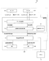
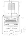
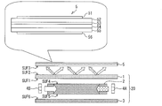
- FIG. 1 is a diagram showing a schematic configuration of a display device 100 according to the present embodiment.
- FIG. 2 is a block diagram showing a configuration of the calculation unit 7 and members related to the calculation unit 7 in the display device 100.
- a display device 100 shown in FIG. 1 includes an optical path changing member 1, a light guide plate 2, a reflection sheet 3, LEDs 4A and 4B, a display unit 5, sensors 6A and 6B, a calculation unit 7, a light source drive control unit 8, a frame frame 9, and A memory 10 is provided.
- the LEDs 4 ⁇ / b> A and 4 ⁇ / b> B and the light source drive control unit 8 are components of the backlight unit 300 that illuminates the display unit 5 from the back surface of the display unit 5.
- front in the present specification means a surface on the side where the display unit 5 displays an image (that is, the side on which the user views the display unit 5).
- rear surface in the present specification means a surface on the opposite side to the side on which the display unit 5 displays an image.
- the display unit 5 shown in FIG. 1 is a dual view display.
- the optical path changing member 1 is disposed on the back surface of the display unit 5.
- the light path changing member 1 has a light guide plate 2 disposed on the back surface thereof.
- the light guide plate 2 has a reflection sheet 3 disposed on the back surface thereof.
- LED4A and 4B are arrange
- LEDs (light sources) 4 ⁇ / b> A and 4 ⁇ / b> B are light sources for illuminating the display unit 5 from the back surface of the display unit 5.
- LED4A is provided in the position which radiate
- LED4B is provided in the position which radiate
- the light guide plate 2 is a plate on which irregularities such as V-shaped grooves or dot-shaped openings are formed.
- the light guide plate 2 emits uniform light from the front surface of the light guide plate 2, that is, the surface on the optical path changing member 1 side, by diffusing the light incident from each of the LEDs 4A and 4B.
- the light incident on the light guide plate 2 from the LED 4A is emitted from the front surface of the light guide plate 2 at an angle corresponding to, for example, a viewing angle of 70 ° ⁇ 5 °.
- the light incident on the light guide plate 2 from the LED 4B is emitted from the front surface of the light guide plate 2 at an angle corresponding to, for example, a viewing angle of ⁇ 70 ° ⁇ 5 °.
- the viewing angle when the display unit 5 is viewed from the frontal direction, the viewing angle is 0 °, and when the display unit 5 is inclined from the viewing angle 0 ° to the A side, the angle is +, and the viewing angle is 0 °. When it is inclined to the B side, the angle is set to-.
- the reflection sheet 3 is used to reflect a part of the light emitted from the back surface of the light guide plate 2 and collect it on the front surface of the light guide plate 2.
- the optical path changing member 1 is constituted by, for example, an optical sheet, a diffusion sheet, or a prism sheet.
- the optical path changing member 1 changes the optical path of each light incident from the light guide plate 2 to a desired optical path, and emits the light after the optical path change from the front of the optical path changing member 1, that is, the surface on the display unit 5 side. .
- the light incident on the optical path changing member 1 from the LED 4A through the light guide plate 2 is emitted from the front of the optical path changing member 1 at an angle corresponding to a viewing angle of 45 °, for example.
- the light incident on the optical path changing member 1 from the LED 4B through the light guide plate 2 is emitted from the front of the optical path changing member 1 at an angle corresponding to a viewing angle of ⁇ 45 °, for example.
- the display unit 5 is a display panel capable of simultaneously displaying a plurality of images. Specifically, the display unit 5 has a parallax barrier (parallax barrier) attached to the front thereof, and the parallax barrier separates a plurality of images to be displayed into individual display areas.
- a parallax barrier parallax barrier
- An example of the display unit 5 is an LCD (Liquid Crystal Display).
- the back surface of the display area located on the A side in the display unit 5 is illuminated by light emitted from the optical path changing member 1 through the light guide plate 2 from the LED 4A.
- a luminance peak is obtained at a viewing angle of 45 °.
- the back surface of the display area located on the B side in the display unit 5 is illuminated by the light emitted from the optical path changing member 1 through the light guide plate 2 from the LED 4B.
- a luminance peak is obtained at a viewing angle of ⁇ 45 °.
- the luminance peak for the image displayed on the A side of the display unit 5 and the luminance peak for the image displayed on the B side of the display unit 5 are in different directions.
- the viewing angle at which the luminance peak can be obtained for each of the images displayed on the A side and the B side of the display unit 5 can be set to a desired angle. It is possible to improve the display quality of the image.
- the display device 100 it is not necessary to increase the intensity of light that illuminates the front direction with respect to the display unit 5 in order to obtain a desired luminance in a direction other than the front direction (viewing angle 0 °) with respect to the display unit 5. Thus, power consumption can be reduced.
- Sensors 6 ⁇ / b> A and 6 ⁇ / b> B are provided on the front side of the display unit 5, that is, on the side where the display unit 5 displays an image, and are provided inside a frame frame 9 as a casing of the display device 100.
- the sensors 6A and 6B are luminance sensors that sense the luminance of light incident on the sensors 6A and 6B.
- the sensor 6A is provided on the path of light emitted from the display area located on the A side in the display unit 5.
- the sensor 6A measures the luminance of the light incident on it, and supplies the result of the measurement as detection data A to the calculation unit 7.
- the sensor 6B is provided on the path of light emitted from the display area located on the B side in the display unit 5.
- the sensor 6B measures the luminance of the light incident on the sensor 6B, and supplies the result of the measurement to the calculation unit 7 as detection data B different from the detection data A.
- the calculation unit 7 includes a data analysis unit 71, a light source emission condition determination unit 72, and a calculation unit memory 73, as shown in FIG.
- the data analysis unit 71 transmits a measurement command signal S_Enable_A to the sensor 6A. In addition, the data analysis unit 71 transmits a measurement command signal S_Enable_B to the sensor 6B.
- the sensor 6A When the sensor 6A receives the measurement command signal S_Enable_A, the sensor 6A starts measuring the luminance, and transmits the measurement result to the data analysis unit 71 as detection data A.
- the sensor 6B receives the measurement command signal S_Enable_B, the sensor 6B starts measuring the luminance, and transmits the measurement result to the data analysis unit 71 as detection data B.
- the data analysis unit 71 receives the detection data A and B.
- the data analysis unit 71 transmits the analysis result A obtained by subjecting the detection data A to AD (Analog-Digital) conversion and noise removal to the light source emission condition determination unit 72.
- the data analysis unit 71 transmits the analysis result B obtained by performing AD conversion and noise removal on the detection data B to the light source emission condition determination unit 72.
- the light source emission condition determination unit 72 receives the analysis result A and the analysis result B.
- the light source emission condition determination unit 72 compares the brightness value measured by the sensor 6A indicated by the analysis result A and the brightness value measured by the sensor 6B indicated by the analysis result B.
- the luminance value measured by the sensor 6A indicated by the analysis result A is It is larger than the luminance value measured by the sensor 6B indicated by the analysis result B.
- the calculation unit memory 73 is constituted by, for example, a ROM (Read Only Memory).
- a look-up table indicating the relationship between the result of the size comparison and the increase / decrease in the current value of the current supplied to the LED 4A and / or LED 4B is recorded in advance.
- the light source emission condition determination unit 72 reads the lookup table from the calculation unit memory 73.
- the look-up table includes information indicating that when the luminance value indicated by the analysis result A is greater than the luminance value indicated by the analysis result B, the current value of the current supplied to the LED 4A is decreased by a predetermined value. Contains. Further, the look-up table indicates that when the luminance value indicated by the analysis result A is smaller than the luminance value indicated by the analysis result B, the current value of the current supplied to the LED 4A is increased by a predetermined value. Contains information.
- the light source light emission condition determining unit 72 drives the light emission condition setting value A that reduces or increases the current value of the current supplied to the LED 4A by a predetermined value according to the information included in the lookup table. Transmit to the control unit 8.
- the light emission condition setting value A indicates the current value of the current supplied to the LED 4A to the light source drive control unit 8. It is a value that is decreased by a predetermined value.
- the light emission condition setting value A indicates the current value of the current supplied to the LED 4A to the light source drive control unit 8. The value is increased by a predetermined value.
- the light emission condition setting value A is the current supplied to the LED 4A to the light source drive control unit 8.
- the current value is a value that decreases by a predetermined value.
- the lookup table indicates that when the luminance value indicated by the analysis result A is greater than the luminance value indicated by the analysis result B, the current value of the current supplied to the LED 4B is increased by a predetermined value. Information may be included. Further, the lookup table indicates that when the luminance value indicated by the analysis result A is smaller than the luminance value indicated by the analysis result B, the current value of the current supplied to the LED 4B is reduced by a predetermined value. Information may be included. In this case, the light source light emission condition determination unit 72 sets the light emission condition to increase or decrease the current value of the current supplied to the LED 4B according to the same principle as the light emission condition setting value A that increases or decreases the current value of the current supplied to the LED 4A. The value B is transmitted to the light source drive control unit 8.
- the light source drive control unit 8 receives the light emission condition setting value A or the light emission condition setting value B.
- the light source drive control unit 8 can be constituted by, for example, a general LED drive circuit that drives the LEDs 4A and 4B by supplying current to the LEDs 4A and 4B.
- the light source drive control unit 8 can easily generate the light source control signal A, which is the current supplied to the LED 4A, based on the light emission condition setting value A. That is, in this example, the light source drive control unit 8 may reduce the current value of the light source control signal A based on the light emission condition setting value A.
- the light source drive control unit 8 can easily generate the light source control signal B, which is the current supplied to the LED 4B, based on the light emission condition setting value B. That is, in this example, the light source drive control unit 8 may increase the current value of the light source control signal B based on the light emission condition setting value B.
- the difference between the luminance value indicated by the analysis result A and the luminance value indicated by the analysis result B is a certain value (for example, the current value of the current supplied to the LED 4A or 4B in one operation).
- the operation is terminated when it becomes less than the value of brightness, which is changed by raising or lowering.
- the difference between the brightness value indicated by the analysis result A (the brightness value measured by the sensor 6A) and the brightness value indicated by the analysis result B (the brightness value measured by the sensor 6B) refer to the analysis results A and B. Then, the light source emission condition determination unit 72 may obtain it.
- the light source drive control unit 8 may be configured to be able to read information recorded in the memory 10 or record information in the memory 10. Thereby, information indicating the current value of the current supplied to the LEDs 4A and / or 4B at the end of the operation is recorded in the memory 10, or the current value of the light source control signal A corresponding to the light emission condition setting value A is stored from the memory 10.
- the current value of the light source control signal B corresponding to the light emission condition setting value B can be read from the memory 10.
- the position where the memory 10 is provided may be in the backlight unit 300 or in another display device 100.
- said structure displays on the A side of the display part 5 due to the solid dispersion
- these luminances can be made substantially uniform. According to said structure, it becomes possible to adjust the appearance of an image in the environment close
- each LED 4A and 4B pseudo white LED, high color rendering LED, etc. can be used.
- each of the LEDs 4A and 4B may be replaced with CCFT (Cold Cathode Fluorescent Tube).
- CCFT Cold Cathode Fluorescent Tube
- the light source drive control unit 8 adjusts (increases or decreases) the current value of the current (light source control signal A) supplied to the LED 4A based on the light emission condition setting value A (Process A). Or a process (process B) for adjusting (increasing or decreasing) the current value of the current (light source control signal B) supplied to the LED 4B based on the light emission condition set value B is performed.
- the display device 100 according to the embodiment is not limited to this, and may be configured to execute both the process A and the process B.
- the light source drive control unit 8 is based on the light emission condition setting value A.
- a configuration may be adopted in which the current value of the light source control signal A is decreased (processing A) and the current value of the light source control signal B is increased based on the light emission condition setting value B (processing B).
- the calculation unit 7 in the present display device 100 performs processing for reducing the luminance of the light source that illuminates the display area where the luminance of the emitted light is high, and the emitted light based on the measurement results of the sensors 6A and 6B. At least one of the processes of increasing the luminance of the light source that illuminates the display area where the luminance of light is low is performed.
- the processing of the calculation unit 7 is the same in the following embodiments.
- RGB-LED composed of LEDs of three colors of red (R), green (G), and blue (B) can be used.
- RGB-LEDs are used as the LEDs 4A and 4B
- Sensors 6A and 6B measure luminance and chromaticity, and transmit the measurement results to calculation unit 7.
- the chromaticity is usually expressed by chromaticity coordinates (x, y).
- RGB-LED is used as the light source
- the ratio of currents supplied to the red, green, and blue LEDs is adjusted.
- the chromaticity at white time is defined as, for example, chromaticity coordinates (0.3, 0.3), and the current supplied to the red, green, and blue LEDs is adjusted so that the chromaticity is at white time.
- the A side chromaticity is measured by the sensor 6A, and the B side chromaticity is changed to the A side chromaticity. Go together.
- the B side chromaticity may be measured by the sensor 6B, and the A side chromaticity may be matched with the B side chromaticity.
- the chromaticity of the LEDs 4A and / or 4B may be matched with a predetermined target chromaticity (for example, (0.3, 0.3)) during white lighting.
- a look-up table related to chromaticity indicating the relationship between the chromaticity coordinates and the current value of the current supplied to the LED 4A and / or the LED 4B is recorded in advance.
- the lookup table related to the chromaticity matches these chromaticity coordinates.
- Information indicating that the current value of the current supplied to the LED 4A is changed by a predetermined value is included.
- the light source emission condition determination unit 72 transmits to the light source drive control unit 8 a light emission condition setting value that changes the current value of the current supplied to the LED 4A by a predetermined value according to the lookup table related to the chromaticity.
- the light emission condition setting value is set to the light source drive control unit 8 with these colors. It is a value that changes the current value of the current supplied to the LED 4A by a predetermined value so that the degree coordinates coincide.
- the look-up table for chromaticity is such that when the chromaticity coordinates of the chromaticity measured by the sensor 6A and the chromaticity coordinates of the chromaticity measured by the sensor 6B are different, these chromaticity coordinates are matched.
- Information that changes the current value of the current supplied to the LED 4B by a predetermined value may be included.
- the calculation unit 7 sets the light emission condition setting value for changing the current value of the current supplied to the LED 4B to the light source drive control unit 8 based on the same principle as the light emission condition setting value for changing the current value of the current supplied to the LED 4A. Send to.
- the light source drive controller 8 generates a current to be supplied to the LED 4A and / or the LED 4B based on the light emission condition setting value, and drives the LED 4A and / or the LED 4B by supplying the current to the LED 4A and / or the LED 4B. .
- chromaticity coordinates (x, y) (0.3, 0.3)
- the number of sensors is not particularly limited.
- the display device 100 may include three or more of the sensors.
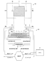
- the display device 100 may be configured to include one such sensor. An example of this configuration is shown in FIG.
- 3 includes one sensor 6 instead of the sensors 6A and 6B.
- the sensor 6 is provided on the front side of the display unit 5 and is provided inside the frame 9.
- the sensor 6 is provided inside the frame 9 on the upper side in the plan view, which is defined by a two-dot chain line.
- the senor 6 is preferably provided at a position where the distance to the LED 4A is equal to the distance to the LED 4B. This is because the distance between the LEDs 4A and 4B is made uniform to measure the light emitted from the display area located on the A side in the display unit 5 and the display located on the B side in the display unit 5. This is because the measurement of the light emitted from the region is performed under the same conditions as much as possible.
- the LED 4A is made to emit light with the LED 4B turned off, and the measurement result of the sensor 6 is measured with the measurement result of light emitted from the display region located on the A side (corresponding to the detection data A). To do. Subsequently, the LED 4A is turned off and the LED 4B is caused to emit light, and the measurement result of the sensor 6 is taken as a measurement result (corresponding to the detection data B) of the light emitted from the display area located on the B side.
- the sensor 6 also functions as the sensors 6A and 6B, the calculation unit 7 and members related to the calculation unit 7 are easily operated based on the configuration of the block diagram shown in FIG. 2 and the description thereof. It is possible.
- the senor 6 is a luminance sensor
- the sensor 6 may of course be a color sensor.
- the display device 100 includes a plurality of sensors like the sensors 6A and 6B shown in FIG. 1, the same number of sensors are provided on each of the A side and the B side. preferable. This is because by providing the same number of sensors on each of the A side and the B side, the measurement of light emitted from the display area located on the A side in the display unit 5 and the B side in the display unit 5 are performed. This is because the measurement of light emitted from the display area located is performed under the same conditions as much as possible.
- the display device 100 is preferably configured according to the first embodiment. This makes it possible to make the luminance of the image displayed on the A side of the display unit 5 uniform with the luminance of the image displayed on the B side of the display unit 5 (see FIG. 4).
- FIG. 4 shows an example in which both the luminance of the image displayed on the A side of the display unit 5 and the luminance of the image displayed on the B side of the display unit 5 are brightened to achieve uniformity. Yes.
- the uniform brightness and darkness can be appropriately determined according to whether the current supplied to the LED 4A or 4B is increased or decreased in the configuration of FIG.
- the display device 100 is preferably configured according to the second embodiment. Thereby, it is possible to make the luminance of the image displayed on the A side of the display unit 5 uniform with the luminance of the image displayed on the B side of the display unit 5. In addition, this makes it possible to equalize the chromaticity (hue) of the image displayed on the A side of the display unit 5 and the chromaticity (hue) of the image displayed on the B side of the display unit 5. This is possible (see FIG. 4).
- the display device 100 it is possible to reduce the difference in appearance between the images displayed on the display unit 5.
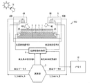
- the display device 100 can also set the luminance (and chromaticity) of the image displayed on the A side and / or B side of the display unit 5 to an arbitrary value (chromaticity coordinates). An example in which this is suitable will be described with reference to FIG.
- the external light 11 is inserted into the display area on the A side in the display unit 5.
- the display quality is remarkably deteriorated.
- the display quality is improved by increasing the luminance of the backlight. That is, since it is necessary to increase the luminance of the light emitted from the corresponding LED, in this case, the luminance of the light emitted from the LED 4A needs to be larger than the luminance of the light emitted from the LED 4B.
- the outside light luminance is sensed by the sensors 6A and 6B. Based on the sensed data, analyze which external light intensity is greater.
- the light source emission condition determination unit 72 increases the current value of the current supplied to the LED 4A in the display ON state (backlight ON) in order to improve the display quality on the side where the external light luminance is large (for example, the A side in FIG. 5).
- the look-up table includes information indicating that the current value supplied to the LEDs 4A and 4B is changed by a predetermined current value based on the external light luminance measured by the sensor.
- the drive control of the LEDs 4A and 4B according to the above-described embodiments is current control in which the amplitude of the current supplied to the LEDs 4A and 4B is variable.
- PWM Pulse Width Modulation
- the display device 100 can achieve the same effects as those of the above-described embodiments. Such a display device 100 will be described in the present embodiment. To do.
- the display device 100 has the same configuration as that shown in FIGS. And about the flow of operation
- the arithmetic unit memory 73 In the arithmetic unit memory 73, the result of comparing the brightness value indicated by the analysis result A and the brightness value indicated by the analysis result B, and the current supplied to the LED 4A and / or LED 4B during one cycle. A lookup table showing the relationship with the change in duty ratio is recorded in advance.
- the light source emission condition determination unit 72 reads the lookup table from the calculation unit memory 73.
- the look-up table includes information indicating that when the luminance value indicated by the analysis result A is greater than the luminance value indicated by the analysis result B, the duty ratio of the current supplied to the LED 4A is reduced by a predetermined ratio. Contains. Further, the lookup table indicates that when the luminance value indicated by the analysis result A is smaller than the luminance value indicated by the analysis result B, the duty ratio of the current supplied to the LED 4A is increased by a predetermined ratio. Contains information.
- the light source emission condition determination unit 72 changes the light emission condition setting value A for changing the duty ratio of the current supplied to the LED 4A by a predetermined ratio in accordance with the information included in the lookup table. 8 to send.
- the light emission condition setting value A indicates the duty ratio of the current supplied to the LED 4A to the light source drive control unit 8. It is a value that is reduced by a predetermined ratio.
- the light emission condition setting value A indicates the duty ratio of the current supplied to the LED 4A to the light source drive control unit 8. The value is increased by a predetermined ratio.
- the lookup table indicates that when the luminance value indicated by the analysis result A is greater than the luminance value indicated by the analysis result B, the duty ratio of the current supplied to the LED 4B is increased by a predetermined ratio. Information may be included.
- the lookup table indicates that when the luminance value indicated by the analysis result A is smaller than the luminance value indicated by the analysis result B, the duty ratio of the current supplied to the LED 4B is reduced by a predetermined ratio. Information may be included.
- the light source light emission condition determining unit 72 uses the same principle as the light emission condition setting value A for changing the duty ratio of the current supplied to the LED 4A, and the light emission condition setting value B for changing the duty ratio of the current supplied to the LED 4B. It transmits to the light source drive control part 8.
- the light source drive control unit 8 receives the light emission condition setting value A or the light emission condition setting value B.
- the light source drive control unit 8 can be constituted by, for example, a general LED drive circuit that drives the LEDs 4A and 4B by supplying a current subjected to PWM modulation to the LEDs 4A and 4B.
- the light source drive control unit 8 can easily generate the light source control signal A, which is the current supplied to the LED 4A, based on the light emission condition setting value A. That is, the light source drive control unit 8 may change the duty ratio of the current of the light source control signal A based on the light emission condition setting value A.
- the light source drive control unit 8 can easily generate the light source control signal B, which is the current supplied to the LED 4B, based on the light emission condition setting value B. That is, the light source drive control unit 8 may change the duty ratio of the current of the light source control signal B based on the light emission condition setting value B.
- the difference between the luminance value indicated by the analysis result A and the luminance value indicated by the analysis result B corresponds to a certain value (for example, a current duty ratio that is expanded and contracted by one operation. When it becomes less than (luminance value), the operation is terminated.
- a certain value for example, a current duty ratio that is expanded and contracted by one operation.
- the operation is terminated.
- the light source emission condition determination unit 72 may obtain it.
- the display device 100 displays on the A side of the display part 5 due to the solid dispersion
- the luminance of the image and the luminance of the image displayed on the B side of the display unit 5 are different, these luminances can be made substantially uniform. That is, the display device 100 can achieve the same effects as those of the above-described embodiments even when the drive control of the LEDs 4A and 4B is PWM.
- RGB-LEDs are used as the LEDs 4A and 4B
- color sensors are used as the sensors 6A and 6B, respectively.
- a look-up table related to chromaticity indicating the relationship between the chromaticity coordinates and the duty ratio of the current supplied to the LED 4A and / or the LED 4B is recorded in advance.
- the lookup table related to the chromaticity matches these chromaticity coordinates.
- Information indicating that the duty ratio of the current supplied to the LED 4A is changed by a predetermined ratio is included.
- the light source emission condition determination unit 72 transmits to the light source drive control unit 8 a light emission condition setting value that changes the duty ratio of the current supplied to the LED 4A by a predetermined ratio according to the lookup table related to the chromaticity.
- the light emission condition setting value is set to the light source drive control unit 8 with these colors. This is a value that changes the duty ratio of the current supplied to the LED 4A by a predetermined ratio so that the degree coordinates coincide.
- the look-up table for chromaticity is such that when the chromaticity coordinates of the chromaticity measured by the sensor 6A and the chromaticity coordinates of the chromaticity measured by the sensor 6B are different, these chromaticity coordinates are matched.
- Information that changes the duty ratio of the current supplied to the LED 4B by a predetermined ratio may be included.
- the calculation unit 7 sets the light emission condition setting value for changing the duty ratio of the current supplied to the LED 4B to the light source drive control unit 8 according to the same principle as the light emission condition setting value for changing the duty ratio of the current supplied to the LED 4A. Send to.
- the light source drive controller 8 generates a current to be supplied to the LED 4A and / or the LED 4B based on the light emission condition setting value, and drives the LED 4A and / or the LED 4B by supplying the current to the LED 4A and / or the LED 4B. .
- the technology according to the present embodiment may be combined with the technology according to the embodiment according to FIG. That is, instead of the sensors 6A and 6B, a single sensor 6 may be used to measure luminance (and further chromaticity, if necessary) in the manner described above.
- the light source drive control unit 8 adjusts the duty ratio (the ratio is large or small) of the current (light source control signal A) supplied to the LED 4A based on the light emission condition setting value A (process A). Or the processing (processing B) of adjusting the duty ratio of the current (light source control signal B) supplied to the LED 4B based on the light emission condition setting value B (the ratio is large or small) is performed.
- the display device 100 according to the embodiment is not limited to this, and may be configured to execute both the process A and the process B.
- the light source drive control unit 8 is based on the light emission condition setting value A.
- a configuration may be employed in which the duty ratio of the light source control signal A is decreased (Processing A) and the duty ratio of the light source control signal B is increased based on the light emission condition setting value B (Processing B).
- the calculation unit 7 in the present display device 100 performs processing for reducing the luminance of the light source that illuminates the display area where the luminance of the emitted light is high, and the emitted light based on the measurement results of the sensors 6A and 6B. At least one of the processes of increasing the luminance of the light source that illuminates the display area where the luminance of light is low is performed.
- the processing of the calculation unit 7 is the same in the following embodiments.
- FIG. 6 shows the configuration of the display device 100 according to this embodiment.
- the sensor 6A shown in FIG. 6 is provided on the path of light emitted from the display area located on the A side in the display unit 5.
- the sensor 6B shown in FIG. 6 is provided on the path of light emitted from the display area located on the B side in the display unit 5. 6 is different from that shown in FIG. 1 in that neither of the sensors 6A and 6B shown in FIG. However, the functions of the sensors 6A and 6B are the same as those shown in FIG.
- the members for providing the sensors 6A and 6B are not particularly limited as long as they are other than the display device 100. Therefore, for the sake of convenience, in FIG. 6, detailed illustration of members that support the sensors 6A and 6B is omitted.
- the sensors 6A and 6B measure the luminance and detect the detection data A and B, respectively, in the same manner as shown in FIGS. Is transmitted to the data analysis unit 71.
- the configurations and operations of the data analysis unit 71, the light source emission condition determination unit 72, and the calculation unit memory 73 are the same as those shown in FIG.
- the light source drive control unit 8 makes the luminances of the images displayed on the A side and the B side of the display unit 5 substantially uniform with each other (the adjustment of the luminance of the LEDs 4A and 4B is completed).
- the received light emission condition setting values A and B are recorded in the memory 10.
- the light source drive control unit 8 reads the light emission condition setting values A and B previously recorded in the memory 10, and the light emission condition setting values A and B are read. Based on B, the brightness of the LEDs 4A and 4B is set.
- the technology according to the present embodiment can be expressed as follows.
- a control method for a display device 100 including a display unit 5 having a plurality of display areas, and a plurality of LEDs 4A and 4B that illuminate the display unit 5 from the back of the display unit 5 and illuminate different display areas.
- the light emission condition setting values A and B received last are recorded in the memory 10 and the LEDs 4A and 4B need to emit light
- the light emission condition settings previously recorded in the memory 10 are recorded.
- the light source drive control unit 8 may be operated so as to read the values A and B and set the luminance of the LEDs 4A and 4B based on the light emission condition setting values A and B.
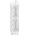
- FIGS. 7A and 7B are perspective views showing the configuration of the display device 110 according to the present embodiment.
- 7A is a view of the display device 110 viewed from the C side
- FIG. 7B is a view of the display device 110 viewed from the D side.
- FIG. 8 is a diagram showing a schematic configuration of the display device 110 according to the present embodiment, corresponding to FIG. However, for convenience of illustration, only a plan view of the display device 110 corresponding to FIG. 1 is shown in FIG.
- the display unit 5 of the display device 100 is a dual view display.
- the display unit 5 of the display device 110 is a quartet view display.
- the display device 110 includes LEDs 4C and 4D and sensors 6C and 6D in addition to the configuration of the display device 100 shown in FIG. Among these, it can be said that the LEDs 4 ⁇ / b> C and 4 ⁇ / b> D are components of the backlight unit 300.
- LEDs (light sources) 4C and 4D are light sources for illuminating the display unit 5 from the back surface of the display unit 5 disposed on the side surface of the light guide plate 2 in the same manner as the LEDs 4A and 4B.
- LED4C is provided in the position which radiate
- LED4D is provided in the position which radiate
- the straight line connecting LED 4A and LED 4B is orthogonal to the straight line connecting LED 4C and LED 4D.
- the positional relationship of LED 4D with respect to LED 4C is equal to the positional relationship of LED 4B with respect to LED 4A.
- the optical path changing member 1, the light guide plate 2, and the reflection sheet 3 exert the same function as the light emitted from the LEDs 4A and 4B on the light emitted from the LEDs 4C and 4D.
- the viewing angle when viewing the display unit 5 from the front direction, the viewing angle is 0 °, and when the viewing angle is tilted from the viewing angle 0 ° to the C side, the angle is set to + and the viewing angle is tilted from the viewing angle 0 ° to the D side.
- the angle is-.
- the angle in order to distinguish between an angle inclined to the A side and an angle inclined to the C side, and to distinguish between an angle inclined to the B side and an angle inclined to the D side, the angle is inclined to the C side or D side.
- [] is added to the angle display.
- the light incident on the optical path changing member 1 from the LED 4C through the light guide plate 2 is emitted from the front of the optical path changing member 1 at an angle corresponding to, for example, a viewing angle [45 °].
- the light incident on the optical path changing member 1 from the LED 4D through the light guide plate 2 is emitted from the front of the optical path changing member 1 at an angle corresponding to, for example, a viewing angle [ ⁇ 45 °].
- the back surface of the display area located on the C side in the display unit 5 is illuminated with light emitted from the optical path changing member 1 through the light guide plate 2 from the LED 4C. Thereby, with respect to the image displayed in the display area located on the C side, a luminance peak is obtained at the viewing angle [45 °].
- the back surface of the display region located on the D side in the display unit 5 is illuminated by light emitted from the optical path changing member 1 through the light guide plate 2 from the LED 4D.
- a luminance peak is obtained at the viewing angle [ ⁇ 45 °].
- the luminance peak for the image displayed on the A side of the display unit 5 the luminance peak for the image displayed on the B side of the display unit 5, and the image displayed on the C side of the display unit 5
- the luminance peak for the image and the luminance peak for the image displayed on the D side of the display unit 5 are in different directions.
- the viewing angle at which the luminance peak can be obtained for each of the images displayed on the A side-D side of the display unit 5 can be set to a desired angle. It is possible to improve the display quality of the image.
- the display device 110 in order to obtain a desired luminance in a direction other than the direction directly in front of the display unit 5 (viewing angles 0 ° and [0 °]), the intensity of light that illuminates the direction in front of the display unit 5 is increased. Therefore, it is possible to reduce power consumption.
- Sensors 6 ⁇ / b> C and 6 ⁇ / b> D are provided on the front side of the display unit 5, that is, on the side where the display unit 5 displays an image, and are provided inside a frame frame 9 as a casing of the display device 110.
- the sensors 6C and 6D are luminance sensors that sense the luminance of light incident on the sensors 6C and 6D.
- the sensor 6C is provided on the path of light emitted from the display area located on the C side in the display unit 5.
- the sensor 6C measures the luminance of the light incident on the sensor 6C, and supplies the result of the measurement to the calculation unit 7 as detection data C different from the detection data A and B.
- the sensor 6D is provided on a path of light emitted from the display area located on the D side in the display unit 5.
- the sensor 6D measures the luminance of the light incident thereon, and supplies the result of the measurement to the calculation unit 7 as detection data D different from the detection data AC.
- the LEDs 4C and 4D and the sensors 6C and 6D are members corresponding to the LEDs 4A and 4B and the sensors 6A and 6B, respectively, and have the same configuration as the LEDs 4A and 4B and the sensors 6A and 6B.
- the display device 110 includes the display device 100 having the cross section shown in FIG. Further, the display device 110 has the same configuration as the cross section shown in FIG. 1 including the LEDs 4C and 4D and the sensors 6C and 6D in the cross sections on the C side and the D side.
- the calculation unit 7 of the display device 110 includes two configurations of the calculation unit 7 shown in FIG. That is, the calculation unit 7 of the display device 110 includes the configuration illustrated in FIG. 2 that adjusts the luminance of the LEDs 4A and 4B and the configuration illustrated in FIG. 2 that adjusts the luminance of the LEDs 4C and 4D. Each of these two configurations exerts the same operation and function on the two corresponding LEDs, and thus a detailed description of the operation and function will be omitted.
- the display part 5 displays on the C side of the display part 5 due to the solid dispersion
- these luminances can be made substantially uniform.
- the technology according to each embodiment described above applied to the configuration for adjusting the luminance of the LEDs 4A and 4B may be combined with the configuration for adjusting the luminance of the LEDs 4C and 4D.
- a color sensor may be used as the sensor 6A-6D instead of the luminance sensor.
- the light emission control of the LEDs 4C and 4D may be current control or PWM control.
- the brightness may be adjusted by using a sensor at the time of inspection before shipment without mounting the sensor on the display device 110 as a final product.
- the luminance values on the A side and the D side are not limited to the same value, and the values of the respective luminances (and further chromaticity values as necessary) can be set to arbitrary values.
- the brightness of the LED as a light source is adjusted by measuring the brightness value (and, if necessary, the value of chromaticity).
- the dual view display separates images in two directions by attaching a parallax barrier (parallax barrier) to the display unit 5. If the parallax barrier is affixed, the area where light can be transmitted differs between the A side and the B side of the display unit 5, which may cause a difference in luminance.
- a parallax barrier parallax barrier
- the luminance of the image displayed on the A side of the display unit 5 and the luminance of the image displayed on the B side of the display unit 5 are different from each other due to the deviation of the attachment of the parallax barrier. In addition, these luminances are made substantially uniform.
- the display device 100 according to the present embodiment is equivalent to a configuration using an image sensor as the sensor 6 shown in FIG.
- the calculation unit 7 calculates each transmissive area on the A side and the B side of the display unit 5 based on the amount of deviation.
- the light source drive control unit 8 calculates the current value (or current duty ratio) of the current supplied to the LEDs 4A and 4B based on each transmissive area calculated by the calculation unit 7, and based on the calculated current value, The brightness of the LEDs 4A and 4B is adjusted.
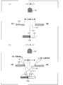
- FIG. 13 are image diagrams for explaining functions of the display device 100 according to the present embodiment.
- FIG. 13A shows a case where there is no deviation
- FIG. 13B shows a case where there is the deviation.
- the image sensor 135 measures the distance from the center 134c of the BM 134 to the A-side end of the opening 131 and the distance from the center 134c to the B-side end of the opening 131. Thereby, the image sensor 135 can easily measure the amount of deviation of the attachment of the parallax barrier 130 from these two distances.
- the light source emission condition determination unit 72 of the calculation unit 7 calculates the size (or a ratio) of the transmissive area in each of the display areas on the A side and the B side based on the shift amount measured by the image sensor 135. .
- the distance from the center 134c to the A-side end of the opening 131 is shorter than the distance from the center 134c to the B-side end of the opening 131. Therefore, based on the principle of the dual view display, the transmissive area on the A side in the display unit 5 is larger than that on the B side in the display unit 5, and the transmissive area of the A side pixel is the transmissive area of the B side pixel. You can see that it is wider.
- the light source emission condition determination unit 72 obtains a current value (or duty ratio) to be supplied to the LED 4A or 4B based on the size of the transmissive area of each display area on the A side and the B side. That is, in the example shown in FIG. 13B, the current value of the current supplied to the LED 4A is decreased by a predetermined value in order to reduce the luminance of the LED 4A that emits light toward the A side having a large transmissive area. Let Of course, instead of decreasing the current value, the duty ratio of the current supplied to the LED 4A may be reduced by a predetermined ratio. Instead of changing the current supplied to the LED 4A, the current supplied to the LED 4B may be changed.
- the light source drive controller 8 generates a current to be supplied to the LED 4A and / or the LED 4B based on the light emission condition setting value, and drives the LED 4A and / or the LED 4B by supplying the current to the LED 4A and / or the LED 4B. . In this way, it is possible to optimally control the luminance values on the A side and B side in the display unit 5.
- the brightness may be adjusted using the image sensor at the time of inspection before shipment, etc. without mounting the image sensor on the display device 100 as the final product.
- the optical path changing member 1 is a kind of so-called optical sheet that plays a role of reflecting, diffusing, and condensing light emitted from the light guide plate 2, but as described above, the optical path changing member 1 of the present embodiment is at least It is a member that changes the optical path of incident light due to its optical characteristics.
- the optical path changing member 1 includes a light incident surface SUF1 on which light emitted from each of the two LEDs 4A and 4B arranged opposite to each other in the left-right direction with respect to the paper surface, and a light incident surface And a light exit surface SUF2 from which light incident from the SUF1 exits. Further, the light incident surface SUF1 and the light emitting surface SUF2 face each other in the vertical direction with respect to the paper surface.
- the optical path changing member 1 has a light exit surface SUF4 (second light exit surface) with respect to the facing direction of at least two LEDs 4A and 4B.
- optical path changing member 1 optical sheet
- optical sheet optical sheet having such optical characteristics
- FIG. 10A shows a configuration of a BL unit (backlight unit) 20a using a diffusion sheet 1a as the optical path changing member 1, and FIG. 10A uses a lens sheet 1b as the optical path changing member 1.
- FIG. The structure of the existing BL unit (backlight unit) 20b is shown.
- the diffusion sheet 1a shown in FIG. 10 (a) has a fine shape on the sheet surface and scattering materials scattered inside, and in general, the above optical characteristics ( ⁇ ⁇ ) are not direction dependent. However, it is possible to have the above-mentioned optical characteristics with respect to a specific direction. Therefore, in the diffusion sheet 1a, in the case where the optical characteristics are given direction dependency, the optical characteristics are preferably given to the facing direction of the LEDs 4A and 4B.
- the diffusion sheet 1a is less isotropic than the lens sheet 1b described later when the optical characteristics are not direction-dependent, but conversely, the optical characteristics ( ⁇ ⁇ ) are isotropic. Since it can be said that it is provided, it is suitable as an optical path changing member 1 for CV display described later (see FIG. 11).
- the diffusion sheet 1a of the present embodiment is composed of a transparent resin and a light diffusing agent (diffusing fine particles) dispersed in the transparent resin.
- a thermoplastic resin for example, a thermosetting resin, or the like
- a polycarbonate resin an acrylic resin, a fluorine acrylic resin, a silicone acrylic resin, an epoxy acrylate Resins, polystyrene resins, cycloolefin polymers, methylstyrene resins, fluorene resins, polyethylene terephthalate (PET), polypropylene, acrylonitrile styrene copolymers, acrylonitrile polystyrene copolymers, and the like can be used.
- PET polyethylene terephthalate
- the scattering material scattering fine particles
- transparent particles made of an inorganic material or a resin can be used.
- transparent particles made of an inorganic material include particles made of an oxide such as silica (SiO 2 ), alumina (Al 2 O 3 ), magnesium oxide (MgO), titania, or other particles such as calcium carbonate and barium sulfate. Particles can be used.
- Transparent particles made of resin include acrylic resin, styrene resin, acrylic styrene resin or a cross-linked product thereof; melamine formaldehyde resin; polytetrafluoroethylene, perfluoroalkoxy resin, tetrafluoroethylene-hexafluoropropylene copolymer, polyfluorovinylidene And particles made of a fluororesin such as ethylenetetrafluoroethylene copolymer; or a silicone resin can be used.
- the diffusing fine particles having a particle size of the same order as the wavelength of visible light can contribute to the diffusion of light.
- the particle size of the diffusing fine particles needs to be 100 nm or more.
- the particle size of each diffusing fine particle is preferably on the order of larger than the wavelength of visible light, and preferably 1 ⁇ m or more. Therefore, the average particle diameter of the diffusion fine particles is preferably 1 ⁇ m or more, and more preferably about 2 ⁇ m.
- the diffusion sheet 1a particles for expressing light diffusibility are mixed in the transparent resin by about 5% by mass.
- the mixing ratio of the particles is slightly different depending on the desired degree of light diffusivity (for example, defined by the haze value).
- the haze value increases unnecessarily.
- the distance that propagates through the diffusion plate is extended, and the transmittance is extremely lowered.
- the thickness of the diffusion sheet 1a is preferably 0.1 to 5 mm.
- the thickness of the diffusion sheet 1a is 0.1 to 5 mm, optimum diffusion performance and brightness can be obtained, which is preferable in terms of optical characteristics.
- the thickness is less than 0.1 mm, the desired diffusion performance cannot be exhibited.
- the thickness exceeds 5 mm, the amount of resin is large, and the luminance decreases due to absorption, which is not preferable.
- the diffusion sheet 1a of the present embodiment has a haze value of 75% and a total light transmittance of 86%, but the haze value is 70% or more and the total light transmittance is 50% or more. Preferably there is.
- thermoplastic resin When a thermoplastic resin is used as the transparent resin, air bubbles may be used as the scattering material.
- the internal surface of the bubble formed inside the thermoplastic resin causes diffused reflection of light, and a light diffusing function equivalent to or higher than that when light diffusing particles are dispersed can be expressed. Therefore, the film thickness of the diffusion sheet 1a can be made thinner.
- Examples of such a diffusion sheet 1a include white PET and white PP.
- White PET is a resin that is incompatible with PET, fillers such as titanium oxide (TiO 2 ), barium sulfate (BaSO 4 ), and calcium carbonate are dispersed in PET, and then the PET is stretched by a biaxial stretching method. By doing so, bubbles are generated around the filler to form.
- the diffusion sheet 1a made of a thermoplastic resin only needs to be stretched in at least one axial direction. This is because bubbles can be generated around the filler by stretching in at least one axial direction.
- thermoplastic resin examples include acrylonitrile polystyrene copolymer, polyethylene terephthalate (PET), polyethylene-2,6-naphthalate, polypropylene terephthalate, polybutylene terephthalate, cyclohexanedimethanol copolymer polyester resin, isophthalic acid copolymer polyester resin, Polyester resins such as sporoglycol copolymer polyester resin and fluorene copolymer polyester resin, polyolefin resins such as polyethylene, polypropylene, polymethylpentene, and alicyclic olefin copolymer resins, acrylic resins such as polymethyl methacrylate, polycarbonate, Polystyrene, polyamide, polyether, polyesteramide, polyetherester, polyvinyl chloride, cycloolefin polymer And their copolymers and component, also can be used as mixtures of these resins are not particularly limited.
- the thickness of the diffusion sheet 1a is preferably 25 to 500 ⁇ m.
- the thickness of the diffusion sheet 1a is less than 25 ⁇ m, it is not preferable because the sheet is insufficiently squeezed and wrinkles are likely to occur in the manufacturing process and display.
- the thickness of the diffusion sheet 1a exceeds 500 ⁇ m, there is no particular problem with optical performance.
- the rigidity is increased, it is difficult to process into a roll shape and the slit cannot be easily formed. This is not preferable because the advantage of thinness obtained in this manner is reduced.
- the diffusion sheet 1a may have a fine concavo-convex structure formed on the light incident surface SUF1 or the light emitting surface SUF2.
- a method of forming this fine concavo-convex structure when forming the diffusion sheet 1a, it is brought into close contact by applying pressure to a mold for shaping the fine concavo-convex structure by a coextrusion forming method or an injection molding method. There is a method of transferring the concavo-convex structure.
- the fine concavo-convex structure there is a method in which the light incident surface SUF1 or the light exit surface SUF2 of the diffusion sheet 1a is molded using a radiation curable resin such as a UV (Ultra Violet) curable resin. It is done. More specifically, after the diffusion sheet 1a is formed as a plate-like member by a coextrusion method, a fine uneven structure is formed by UV forming an uneven shape on the light incident surface SUF1 or the light exit surface SUF2 of the diffusion sheet 1a. be able to.
- a radiation curable resin such as a UV (Ultra Violet) curable resin.
- the surface state of the light incident surface SUF1 or the light exit surface SUF2 is often expressed in terms of roughness as roughness, but here the surface state is defined as haze value and unevenness spacing Sm value (hereinafter referred to as “Sm value”). It shows with.
- the haze value is defined by JIS K 7136, and is represented by an average value when measured five times using a haze meter.
- the Sm value is defined by the surface roughness standard JIS B0601-2001, and is a contact type surface roughness meter. Means an average value when measured under the condition of a cut-off value of 2.0 mm.
- the unevenness interval is fine but the unevenness roughness is insufficient, and the light surface scattering becomes weak. If it exceeds 900 ⁇ m, the unevenness interval is wide and the roughness becomes rough. Scattering becomes stronger, but it leads to lower front luminance.
- the surface roughness of the light incident surface SUF1 or the light exit surface SUF2 is regular, it is advantageous in obtaining a certain scattering effect as compared with the case where the surface roughness is irregular. It becomes easy.
- the surface condition of the mold is adjusted and transferred in-line during injection molding or extrusion molding. And a method of blasting an abrasive.
- the concentration and particle diameter of the diffusing substance and the thickness of the diffusion layer are adjusted.
- thermoplastic resin is heated and melted with an extruder, extruded from a T-die, and formed into a plate shape.
- the co-extrusion method is used in the case of a laminated plate, and a plurality of extruders are used to carry out lamination extrusion from a lamination die such as a feed block die or a manifold die to form a multilayer plate.
- the lens sheet 1b shown in FIG. 10B a plurality of prism rows 1c are formed on the light emitting surface SUF2, and the ridge line (prism axis) of the prism row 1c of this embodiment is It arrange
- the magnitude of the emission angle ⁇ of the emitted light when the light incident on the incident lens sheet 1b at a predetermined incident angle along the propagation direction of the light emitted from the LEDs 4A and 4B exits from the light exit surface SUF2 side is The incident light is smaller than the incident angle ⁇ . Therefore, there is no problem that it is difficult to emit backlight light having luminance directivity in a plurality of different directions.
- the cross section of the prism row 1c is an isosceles triangle, the apex angle (prism apex angle) is 80 to 100 degrees, and the refractive index is 1.5. It is.
- the emission angle ⁇ approaches 0 degrees.
- the light path changing member 1 has an exit angle ⁇ of light emitted from the light exit surface SUF2 with respect to the facing direction of at least two LEDs 4A and 4B, and is incident on the light incident surface SUF1.
- the light emitted from the LED 4A has a luminance directivity in a direction inclined to the left side (A side, for example, viewing angle +45 degrees) with respect to the normal line of the light exit surface SUF2.
- Light light can be emitted.
- the light emitted from the LED 4B can emit backlight light having luminance directivity in a direction inclined to the right side (B side, for example, a viewing angle of ⁇ 45 degrees) with respect to the normal line. .
- the axis of the prism array is along the propagation direction of the light emitted from the light source, there is no problem that it is difficult to emit backlight light having luminance directivity in a plurality of different directions.
- the light emitted from the light exit surface SUF ⁇ b> 2 of the optical path changing member 1 is directly applied to the external display unit 5.
- the optical sheet between the display unit 5 and the light guide plate 2 described later is composed of only one optical path changing member 1. Therefore, the problem that it is difficult to reduce the thickness does not occur.
- the BL unit 20 it is possible to emit backlight light having luminance directivity in a plurality of different directions while realizing a reduction in thickness.
- the light guide plate 2 is a member that receives light emitted from each of the two LEDs 4A and 4B and guides the received light from the light emitting surface SUF4 to the light incident surface SUF1 of the optical path changing member 1.
- the transparent resin plate converts linear light generated from the LEDs 4A and 4B into a surface light source for entering the display unit 5.
- the shape of the light guide plate 2 is a plate shape (cuboid shape), and the shape of the light exit surface SUF4 (bottom surface SUF5) is a rectangular shape.
- the thickness of the light guide plate 2 is 0.2 mm to 3 mm, but the thickness of the light guide plate 2 is not limited to this range.
- the light guide plate 2 has a plate shape in this embodiment, but various shapes such as a wedge shape and a hull shape can be used. Moreover, as a constituent material of the light guide plate 2, a synthetic resin having a high transmittance such as a methacrylic resin, an acrylic resin, a polycarbonate resin, a polyester resin, or a vinyl chloride resin can be used.
- the light guide plate 2 uses a light exit surface SUF4 that is a mirror surface and the other bottom surface SUF5 is a rough surface.
- the bottom surface SUF5 of the light guide plate 2 is subjected to prism processing, dot printing processing, and the like in order to make the luminance uniform and improve the luminance.
- the LED 4A and 4B are located closer to the farther away from the LEDs 4A and 4B.
- the unevenness is a sparse surface on both ends, and the unevenness is dense at a distant place (near the center of the light guide plate 2), the unevenness formed on the light guide plate 2 is not limited to this form.
- the light guide plate 2 of the present embodiment is configured to emit light uniformly diagonally right upward or diagonally upward left as shown in FIG.
- a method of forming the light guide plate 2 by injection molding using a mold having unevenness, or injecting a light guide member having a flat surface in advance examples thereof include a method of forming by a molding method or a casting method, and printing a special ink so that protrusions are formed by screen printing.
- the reflection sheet 3 is a light reflection member that reflects light leaked from the bottom surface UF5 of the light guide plate 2.
- the surface shape of the reflection sheet 3 is a flat shape.
- a film made of polyester resin or polyolefin resin or a white film is used as the constituent material of the reflection sheet 3.
- a pigment such as titanium oxide, barium sulfate, calcium carbonate, aluminum hydroxide, magnesium carbonate, or aluminum oxide is added to the plastic resin so as to be white. It is formed into a film or sheet. It is also possible to use a resin in which an inorganic filler such as calcium carbonate or titanium oxide is contained, a film is formed, and this is stretched to form a large number of microvoids.
- the LEDs 4A and 4B can make the luminance uniformity in the backlight plane and the light distribution angle distribution of irradiation symmetrical.
- a U-shaped fluorescent tube may be adopted, and one fluorescent tube in which two light sources are connected to each other may be used. Further, two L-shaped fluorescent tubes may be used in combination as a plurality of light sources.
- the LEDs 4A and 4B may include a reflector (not shown).
- the inner surface of the reflector has a parabolic shape, and the LEDs 4A and 4B are arranged at the focal position.
- the display unit 5 has a light irradiation surface SUF3 to which light emitted from the light emission surface SUF4 of the light guide plate 2 is directly irradiated, and includes polarizing plates 51 and 56, a parallax barrier (parallax barrier). ) 52, an adhesive layer 53, a CF (color filter) substrate 54, and a TFT (thin film transistor) substrate 55.
- polarizing plates 51 and 56 polarizing plates 51 and 56, a parallax barrier (parallax barrier). ) 52, an adhesive layer 53, a CF (color filter) substrate 54, and a TFT (thin film transistor) substrate 55.
- the polarizing plates 51 and 56 are a polarizing base material containing a polarizing element, a base substrate (not shown) sandwiching the polarizing substrate between both sides, a protective film (not shown) on one side, and a glass substrate on the other side. It consists of a release film (not shown).
- the polarizing plates 51 and 56 are as thin as about 0.12 mm to 0.4 mm even if about 10 layers are stacked.
- a polarizing substrate containing a polarizing element is iodine or a dichroic dye that is a polarizing element, which causes a polarizing effect.
- As the polarizing substrate polyvinyl alcohol (PVA, Poly Vinyle Alcohol) is used, and the polarizing element is included in this medium.
- Triacetyl cellulose (TAC, Triacetyl cellulose, Cellulose triacetate) is used as a base substrate for protecting the polarizing substrate.
- the release film is coated with an adhesive layer on the base substrate side, peeled off when applied to the glass substrate, and attached to the glass substrate with the adhesive layer.
- the parallax barrier 52 is an optical member in which a light transmission region and a blocking region are formed in a stripe shape, and the parallax barrier 52 separates a plurality of images to be displayed into individual display regions.
- a plurality of different left-side images IL (A) are given to a plurality of users existing in the respective directions of a specific viewing angle L and a viewing angle R.
- Side and right side image IR (B side) can be visually recognized.
- the adhesive layer 53 is a transparent resin layer such as an acrylic resin that adheres the parallax barrier 52 and the CF substrate 54. Note that if the parallax barrier 52 and the CF substrate 54 are formed in contact with each other, the function as a parallax barrier cannot be exerted, so the adhesive layer 53 adjusts the distance between the parallax barrier 52 and the CF substrate 54 to an appropriate distance. This distance may be any distance that allows DV display.
- the CF substrate 54 has a colored layer or a black matrix (BM) that transmits red (R), green (G), and blue (B) light on the substrate corresponding to each pixel, and is a protective film. It's covered.
- This colored layer is a coloring material or a colored film applied to the CF substrate 54 with a fine pattern, and a pigment-based or dye-based one is used.
- the BM layer prevents light leakage during black display and color mixing between adjacent colorants, and also prevents generation of photocurrent due to light irradiation to the TFT substrate 55. Those using a photosensitive material for fixing the coloring material are mixed in the coloring material and fixed as they are.
- a thin BM layer of about 0.1 ⁇ m has a lot of metallic chromium, and carbon, titanium, nickel, etc. are also used. Between the BM layers, three colored layers having a thickness larger than that of the BM layer of about 1.2 ⁇ m are arranged in a certain pattern.
- a high-definition screen has many stripe arrangements of colored layer patterns, but a low-definition screen has a good image quality with a good delta arrangement.
- FIG. 14 is a diagram illustrating a BL unit (backlight unit) 20d which is still another configuration example of the backlight unit.
- BL units 20a, 20b, and 20c The difference from the above-described BL units 20a, 20b, and 20c is that a plurality of light guide plates 2 (and light sources 4A and 4B corresponding thereto) are arranged in the left-right direction.
- the two light guide plates 2L and 2R are arranged so as to be adjacent to each other in the horizontal direction (left-right direction) when the liquid crystal panel 5 is viewed in plan.
- Each of the light guide plates 2L and 2R has the same configuration as that of the light guide plate 2 described above, and LEDs 4A and 4B are arranged on both side surfaces of the light guide plate 2L, respectively, and LEDs 4A and 4B are arranged on both side surfaces of the light guide plate 2R, respectively.
- the set which consists of one light-guide plate 2 and LED4A, 4B corresponding to this is not limited to 2 sets like FIG. 14, It is comprised by 4 sets or more according to the magnitude
- the size of each light guide plate can be reduced by arranging a plurality of light guide plates (light guide plates 2L and 2R in FIG. 14) side by side. The number of reflections of light at can be reduced. Therefore, the liquid crystal panel 5 can be enlarged without causing a change in color (variation) while realizing a reduction in the thickness of the BL unit 20d.
- the plurality of light sources emit light including a predetermined color
- the sensor further measures chromaticity of light emitted from each display region
- the calculation unit The chromaticity of each light source that illuminates each display area is preferably adjusted based on the measurement result of the sensor.
- the calculation unit adjusts the chromaticity of each light source based on the chromaticity of the light emitted from each display area in the display unit, which is a measurement result of the sensor.
- the adjustment since the adjustment is performed using the light emitted from the display unit, a factor that changes the chromaticity of the light after the light is incident on the display unit (that is, after the panel is incident). In consideration of this, it is possible to adjust the chromaticity of the image displayed in each display area.
- the chromaticities of a plurality of images displayed in different display areas can be made substantially uniform. According to said structure, it becomes possible to adjust the color of an image in the environment close
- RGB RedRGBGreen Blue
- LED Light EmittingmDiode: light emitting diode
- the display device of the present invention preferably includes a plurality of sensors that measure the luminance of light emitted from any of the plurality of display areas as the sensor.
- the plurality of display areas display images in different periods, and the sensor emits light emitted from each of the plurality of display areas over the different periods. It is preferable to provide one sensor for measuring the luminance.
- the light source of the light source is controlled to emit light by current control, and the arithmetic unit supplies a current value of a current supplied to the light source that illuminates the display area where the luminance of emitted light is high. It is preferable to perform at least one of a process of reducing the current value and a process of increasing the current value of the current supplied to the light source that illuminates the display area where the luminance of the emitted light is low.
- the light source of the light source is controlled to emit light by pulse width modulation
- the arithmetic unit is a duty of a current supplied to the light source that illuminates the display area where the luminance of emitted light is high. It is preferable to perform at least one of a process of reducing the ratio and a process of increasing the duty ratio of the current supplied to the light source that illuminates the display area where the luminance of emitted light is low.
- the light emission control method for the light source according to the present invention may be current control according to the current value of the current, or the pulse width according to the current pulse width (duty ratio). It may be modulation.
- the number of the plurality of light sources in the display device of the present invention is two or four.
- a parallax barrier for separation into a plurality of the display areas is attached to the display unit, and the amount of misalignment of the parallax barrier is measured as the sensor. It is preferable to include an image sensor.
- the dual view display separates images in two directions by attaching a parallax barrier (parallax barrier) to the display unit. If the parallax barrier is attached with a deviation, the display area of the display unit has a different area where light can be transmitted, which may cause a difference in luminance.
- a parallax barrier parallax barrier
- the plurality of light sources are two light sources arranged opposite to each other, and the display device receives light emitted from each of the two light sources and receives the received light.
- a light guide member having a first light emission surface to be emitted, and a second light emission surface that receives light emitted from the first light emission surface of the light guide member and emits the received light toward the display unit.
- an optical path changing member that changes an optical path of the light passing therethrough, wherein the optical path changing member has a luminance direction in which the luminance distribution in at least two directions different from the normal direction of the display screen of the display unit is maximized. It is preferable to emit light having a property from the second light exit surface.
- the present invention can be used for a display device including a plurality of light sources that illuminate different display areas.
- Examples of such a display device include a dual view display and a quartet view display.
- Optical path changing member 2 Light guide plate 3 Reflective sheet 4A-4D LED (light source) DESCRIPTION OF SYMBOLS 5 Display part 6, 6A-6D Sensor 7 Calculation part 8 Light source drive control part 10 Memory 71 Data analysis part 72 Light source light emission condition determination part 73 Calculation part memory 100, 110 Display apparatus 300 Backlight part
Landscapes
- Engineering & Computer Science (AREA)
- Physics & Mathematics (AREA)
- Computer Hardware Design (AREA)
- General Physics & Mathematics (AREA)
- Theoretical Computer Science (AREA)
- Control Of Indicators Other Than Cathode Ray Tubes (AREA)
- Liquid Crystal (AREA)
- Liquid Crystal Display Device Control (AREA)
Abstract
Description
図1は、本実施の形態に係る表示装置100の概略構成を示す図である。
さらに、各LED4Aおよび4Bとしては、赤(R)、緑(G)、および青(B)の3色のLEDから成るRGB-LEDが利用可能である。
上述した各実施の形態では、表示部5の正面側、すなわち表示部5が画像を表示する側において、自身に入射した光の輝度(必要に応じて、さらに色度)を測定するセンサとして、センサ6Aおよび6Bという2つのセンサを用いていた。
LED4Aおよび4Bに、疑似白色LED、または高演色LEDを用いる場合、表示装置100は、実施の形態1に係る構成であるのが好ましい。これにより、表示部5のA側に表示される画像の輝度と表示部5のB側に表示される画像の輝度との均一化を図ることが可能となる(図4参照)。
上述した各実施の形態に係るLED4Aおよび4Bの駆動制御は、各LED4Aおよび4Bに供給する電流の振幅を可変とする電流制御であった。
センサ6Aおよび6B、センサ6に代表される、輝度センサまたはカラーセンサを表示装置100に搭載しない場合、つまり、最終製品としての表示装置100にセンサを搭載しない場合であっても、上述した各実施の形態に相当する技術を実施することは可能である。以下、その一具体例として、表示装置100にセンサを搭載しない場合に、実施の形態1に相当する技術を実施する例について説明する。
図7の(a)および(b)は、本実施の形態に係る表示装置110の構成を示す斜視図である。図7の(a)は、表示装置110をC側から見た図であり、図7の(b)は、表示装置110をD側から見た図である。
上述した各実施の形態では、輝度の値(必要に応じて、さらに色度の値)を測定することで、光源であるLEDの輝度(必要に応じて、さらに色度)の調整を行った。
光路変更部材1は、導光板2からの出射光を反射,拡散,集光させるなどの役割を持ついわゆる光学シートの一種であるが、上述したとおり、本実施形態の光路変更部材1は、少なくともその光学的特性により入射する光の光路を変更する部材である。
2 導光板
3 反射シート
4A-4D LED(光源)
5 表示部
6、6A-6D センサ
7 演算部
8 光源駆動制御部
10 メモリ
71 データ解析部
72 光源発光条件決定部
73 演算部メモリ
100、110 表示装置
300 バックライト部
Claims (10)
- 複数の表示領域を備えた表示部と、
上記表示部における、互いに異なる上記表示領域を照らす、複数の光源と、
各表示領域から出射された光の輝度を測定する、1または複数のセンサと、
上記センサの測定結果に基づいて、出射された光の輝度が大きい上記表示領域を照らす上記光源の輝度を小さくする処理、および、出射された光の輝度が小さい上記表示領域を照らす上記光源の輝度を大きくする処理のうち少なくともいずれか一方の処理を行う演算部とを備えていることを特徴とする表示装置。 - 上記複数の光源は、所定の色を含む光を出射し、
上記センサは、さらに、各表示領域から出射された光の色度を測定し、
上記演算部は、上記センサの測定結果に基づいて、各表示領域を照らす各光源の色度を調整することを特徴とする請求項1に記載の表示装置。 - 上記センサとして、上記複数の表示領域のいずれかから出射された光の輝度を測定するセンサを複数備えていることを特徴とする請求項1または2に記載の表示装置。
- 上記複数の表示領域は、互いに異なる期間に画像を表示し、
上記センサとして、上記互いに異なる期間に亘って、上記複数の表示領域のそれぞれから出射された光の輝度を測定するセンサを1つ備えていることを特徴とする請求項1または2に記載の表示装置。 - 上記光源は、電流制御により発光が制御されており、
上記演算部は、出射された光の輝度が大きい上記表示領域を照らす上記光源に供給する電流の電流値を小さくする処理、および、出射された光の輝度が小さい上記表示領域を照らす上記光源に供給する電流の電流値を大きくする処理のうち少なくともいずれか一方の処理を行うことを特徴とする請求項1~4のいずれか1項に記載の表示装置。 - 上記光源は、パルス幅変調により発光が制御されており、
上記演算部は、出射された光の輝度が大きい上記表示領域を照らす上記光源に供給する電流のデューティー比を小さくする処理、および、出射された光の輝度が小さい上記表示領域を照らす上記光源に供給する電流のデューティー比を大きくする処理のうち少なくともいずれか一方の処理を行うことを特徴とする請求項1~4のいずれか1項に記載の表示装置。 - 上記複数の光源は、2つまたは4つであることを特徴とする請求項1~6のいずれか1項に記載の表示装置。
- 上記表示部に、複数の上記表示領域への分離を行うための視差バリアが貼り付けられており、
上記センサとして、上記視差バリアの貼り付けのズレ量を測定するイメージセンサを備えていることを特徴とする請求項1に記載の表示装置。 - 上記複数の光源は、互いに対向して配置された2つの光源であり、
上記表示装置は、上記2つの光源のそれぞれから発した光を受け、受けた光を出射する第1光出射面を有する導光部材と、上記導光部材の第1光出射面から出射した光を受け、受けた光を上記表示部に向けて出射する第2光出射面を有し、通過する光の光路を変更する光路変更部材と、を備え、
上記光路変更部材は、上記表示部の表示画面の法線方向とは異なる少なくとも2つの方向の輝度分布が極大となる輝度指向性を有する光を上記第2光出射面から出射することを特徴とする請求項1に記載の表示装置。 - 複数の表示領域を備えた表示部と、
上記表示部における、互いに異なる上記表示領域を照らす、複数の光源とを備えた表示装置の制御方法であって、
1または複数のセンサにより、各表示領域から出射された光の輝度を測定する工程と、
上記センサの測定結果に基づいて、出射された光の輝度が大きい上記表示領域を照らす上記光源の輝度を小さくする工程、および、出射された光の輝度が小さい上記表示領域を照らす上記光源の輝度を大きくする工程のうち少なくともいずれか一方の工程とを含んでいることを特徴とする表示装置の制御方法。
Priority Applications (2)
| Application Number | Priority Date | Filing Date | Title |
|---|---|---|---|
| US14/112,329 US20140246982A1 (en) | 2011-04-22 | 2012-04-16 | Display device, and display device control method |
| JP2013510996A JPWO2012144466A1 (ja) | 2011-04-22 | 2012-04-16 | 表示装置 |
Applications Claiming Priority (2)
| Application Number | Priority Date | Filing Date | Title |
|---|---|---|---|
| JP2011096585 | 2011-04-22 | ||
| JP2011-096585 | 2011-04-22 |
Publications (1)
| Publication Number | Publication Date |
|---|---|
| WO2012144466A1 true WO2012144466A1 (ja) | 2012-10-26 |
Family
ID=47041572
Family Applications (1)
| Application Number | Title | Priority Date | Filing Date |
|---|---|---|---|
| PCT/JP2012/060284 Ceased WO2012144466A1 (ja) | 2011-04-22 | 2012-04-16 | 表示装置、および表示装置の制御方法 |
Country Status (3)
| Country | Link |
|---|---|
| US (1) | US20140246982A1 (ja) |
| JP (1) | JPWO2012144466A1 (ja) |
| WO (1) | WO2012144466A1 (ja) |
Cited By (3)
| Publication number | Priority date | Publication date | Assignee | Title |
|---|---|---|---|---|
| CN107784988A (zh) * | 2016-08-30 | 2018-03-09 | 乐金显示有限公司 | 液晶显示装置和液晶显示装置的局部调光的方法 |
| JP2021533408A (ja) * | 2018-08-03 | 2021-12-02 | マジック リープ, インコーポレイテッドMagic Leap, Inc. | 光学ディスプレイのためのled熱特性評価および較正 |
| JP2022023860A (ja) * | 2016-03-02 | 2022-02-08 | フェイスブック・テクノロジーズ・リミテッド・ライアビリティ・カンパニー | 像面湾曲補正ディスプレイ |
Families Citing this family (10)
| Publication number | Priority date | Publication date | Assignee | Title |
|---|---|---|---|---|
| KR100755676B1 (ko) * | 2005-08-26 | 2007-09-05 | 삼성전자주식회사 | 밝기 향상 및 전력 제어를 지원하는 영상 표시 장치 및방법 |
| US20140028955A1 (en) * | 2011-04-22 | 2014-01-30 | Sharp Kabushiki Kaisha | Backlight unit and display device |
| US10269156B2 (en) | 2015-06-05 | 2019-04-23 | Manufacturing Resources International, Inc. | System and method for blending order confirmation over menu board background |
| US10313037B2 (en) | 2016-05-31 | 2019-06-04 | Manufacturing Resources International, Inc. | Electronic display remote image verification system and method |
| WO2018031717A2 (en) * | 2016-08-10 | 2018-02-15 | Manufacturing Resources International, Inc. | Dynamic dimming led backlight for lcd array |
| DE102018129945A1 (de) * | 2018-11-27 | 2020-05-28 | Osram Opto Semiconductors Gmbh | Optoelektronische anzeigevorrichtung und verfahren zum betrieb einer optoelektronischen anzeigevorrichtung |
| US11176859B2 (en) * | 2020-03-24 | 2021-11-16 | Synaptics Incorporated | Device and method for display module calibration |
| US11895362B2 (en) | 2021-10-29 | 2024-02-06 | Manufacturing Resources International, Inc. | Proof of play for images displayed at electronic displays |
| US20240337869A1 (en) * | 2023-04-04 | 2024-10-10 | Denso International America, Inc. | Selective window darkening system |
| JP2025101400A (ja) * | 2023-12-25 | 2025-07-07 | 日亜化学工業株式会社 | 発光装置及び発光装置の駆動方法 |
Citations (6)
| Publication number | Priority date | Publication date | Assignee | Title |
|---|---|---|---|---|
| JP2002082305A (ja) * | 2000-09-11 | 2002-03-22 | Canon Inc | 画像表示装置および頭部装着型表示装置 |
| JP2004286971A (ja) * | 2003-03-20 | 2004-10-14 | Mitsubishi Electric Corp | 画像表示装置および画像表示方法 |
| JP2005024737A (ja) * | 2003-06-30 | 2005-01-27 | Optrex Corp | 液晶表示装置およびその表示方法 |
| JP2006330187A (ja) * | 2005-05-24 | 2006-12-07 | Sharp Corp | 液晶表示装置、及びその輝度むら補正方法 |
| WO2008035488A1 (en) * | 2006-09-20 | 2008-03-27 | Sharp Kabushiki Kaisha | Display device |
| JP2010160383A (ja) * | 2009-01-09 | 2010-07-22 | Epson Imaging Devices Corp | 表示装置の光学特性測定システム |
Family Cites Families (13)
| Publication number | Priority date | Publication date | Assignee | Title |
|---|---|---|---|---|
| US4233545A (en) * | 1978-09-18 | 1980-11-11 | Webster Lee R | Automatic lighting control system |
| JP4386989B2 (ja) * | 1999-05-11 | 2009-12-16 | パナソニック株式会社 | 液晶表示装置 |
| JP2001210122A (ja) * | 2000-01-28 | 2001-08-03 | Matsushita Electric Ind Co Ltd | 照明装置、映像表示装置、映像表示装置の駆動方法、液晶表示パネル、液晶表示パネルの製造方法、液晶表示パネルの駆動方法、アレイ基板、表示装置、ビューファインダおよびビデオカメラ |
| JP4099496B2 (ja) * | 2002-03-01 | 2008-06-11 | シャープ株式会社 | 発光装置並びに該発光装置を用いた表示装置及び読み取り装置 |
| US7656371B2 (en) * | 2003-07-28 | 2010-02-02 | Nichia Corporation | Light emitting apparatus, LED lighting, LED light emitting apparatus, and control method of light emitting apparatus |
| JP4516467B2 (ja) * | 2005-03-29 | 2010-08-04 | シャープ株式会社 | 面照明装置及びそれを備えた液晶表示装置 |
| KR101119180B1 (ko) * | 2006-01-23 | 2012-03-20 | 삼성전자주식회사 | 광발생 장치 및 이를 갖는 액정 표시 장치 |
| JP5058631B2 (ja) * | 2006-03-03 | 2012-10-24 | 日本電気株式会社 | 光源装置、表示装置、端末装置及びそれらの制御方法 |
| JP2008096928A (ja) * | 2006-10-16 | 2008-04-24 | Toshiba Matsushita Display Technology Co Ltd | 液晶表示装置、液晶表示装置の駆動方法、プログラム、及び記録媒体 |
| JP4803069B2 (ja) * | 2007-02-23 | 2011-10-26 | ソニー株式会社 | 光源装置および液晶表示装置 |
| US8434909B2 (en) * | 2007-10-09 | 2013-05-07 | Flex Lighting Ii, Llc | Light emitting display with light mixing within a film |
| JP5154378B2 (ja) * | 2008-11-21 | 2013-02-27 | 株式会社ジャパンディスプレイウェスト | 表示装置 |
| JP6277549B2 (ja) * | 2014-03-10 | 2018-02-14 | Tianma Japan株式会社 | 面状照明装置及び液晶表示装置 |
-
2012
- 2012-04-16 WO PCT/JP2012/060284 patent/WO2012144466A1/ja not_active Ceased
- 2012-04-16 US US14/112,329 patent/US20140246982A1/en not_active Abandoned
- 2012-04-16 JP JP2013510996A patent/JPWO2012144466A1/ja active Pending
Patent Citations (6)
| Publication number | Priority date | Publication date | Assignee | Title |
|---|---|---|---|---|
| JP2002082305A (ja) * | 2000-09-11 | 2002-03-22 | Canon Inc | 画像表示装置および頭部装着型表示装置 |
| JP2004286971A (ja) * | 2003-03-20 | 2004-10-14 | Mitsubishi Electric Corp | 画像表示装置および画像表示方法 |
| JP2005024737A (ja) * | 2003-06-30 | 2005-01-27 | Optrex Corp | 液晶表示装置およびその表示方法 |
| JP2006330187A (ja) * | 2005-05-24 | 2006-12-07 | Sharp Corp | 液晶表示装置、及びその輝度むら補正方法 |
| WO2008035488A1 (en) * | 2006-09-20 | 2008-03-27 | Sharp Kabushiki Kaisha | Display device |
| JP2010160383A (ja) * | 2009-01-09 | 2010-07-22 | Epson Imaging Devices Corp | 表示装置の光学特性測定システム |
Cited By (4)
| Publication number | Priority date | Publication date | Assignee | Title |
|---|---|---|---|---|
| JP2022023860A (ja) * | 2016-03-02 | 2022-02-08 | フェイスブック・テクノロジーズ・リミテッド・ライアビリティ・カンパニー | 像面湾曲補正ディスプレイ |
| CN107784988A (zh) * | 2016-08-30 | 2018-03-09 | 乐金显示有限公司 | 液晶显示装置和液晶显示装置的局部调光的方法 |
| JP2021533408A (ja) * | 2018-08-03 | 2021-12-02 | マジック リープ, インコーポレイテッドMagic Leap, Inc. | 光学ディスプレイのためのled熱特性評価および較正 |
| JP7555904B2 (ja) | 2018-08-03 | 2024-09-25 | マジック リープ, インコーポレイテッド | 光学ディスプレイのためのled熱特性評価および較正 |
Also Published As
| Publication number | Publication date |
|---|---|
| US20140246982A1 (en) | 2014-09-04 |
| JPWO2012144466A1 (ja) | 2014-07-28 |
Similar Documents
| Publication | Publication Date | Title |
|---|---|---|
| WO2012144466A1 (ja) | 表示装置、および表示装置の制御方法 | |
| WO2012144449A1 (ja) | バックライトユニット及び表示装置 | |
| JP4906831B2 (ja) | 面状照明装置 | |
| US20130314942A1 (en) | Packaging comprising a lightguide | |
| KR20040080295A (ko) | 가시광 확산을 위한 표면 형성된 복합 중합체 렌즈 | |
| CN106133561B (zh) | 反射片、面光源装置用反射单元及面光源装置 | |
| JP2011197656A (ja) | 液晶表示装置 | |
| JP2003279712A (ja) | 透明ポリマーフィルム | |
| JP5104459B2 (ja) | 光学部材とそれを用いたバックライト・ユニット、ディスプレイ | |
| JP2010078980A (ja) | 光制御スタック及びそれを用いたバックライトユニット、表示装置 | |
| CN100590349C (zh) | 面状照明装置 | |
| JP2010044270A (ja) | 光拡散板、光学シート、バックライトユニット及びディスプレイ装置 | |
| JP2010044269A (ja) | 光拡散板、光学シート、バックライトユニット及びディスプレイ装置 | |
| JP2011033643A (ja) | 光路変更シート、バックライトユニット及びディスプレイ装置 | |
| JP2003222714A (ja) | 光反射材料及びそれを用いた光源装置 | |
| JP5332469B2 (ja) | 光学部品、バックライトユニット及び表示装置 | |
| JP5636884B2 (ja) | 導光板、バックライトユニット、表示装置、及び導光板の製造方法 | |
| JP6195882B2 (ja) | 突起を有する光透過板 | |
| WO2012144451A1 (ja) | 照明装置および表示装置 | |
| KR101695203B1 (ko) | 도광판용 시트 결합체 | |
| WO2012144468A1 (ja) | バックライトユニットおよび表示装置 | |
| JP2011133556A (ja) | 光学シート、バックライトユニット及びディスプレイ装置、並びに金型 | |
| JP6195881B2 (ja) | 突起を有する光透過板 | |
| JP5267024B2 (ja) | 光学シート、バックライトユニット及びディスプレイ装置 | |
| KR20130028270A (ko) | 반사 시트 및 그의 제조방법, 반사 시트를 포함하는 액정표시장치 |
Legal Events
| Date | Code | Title | Description |
|---|---|---|---|
| 121 | Ep: the epo has been informed by wipo that ep was designated in this application |
Ref document number: 12773823 Country of ref document: EP Kind code of ref document: A1 |
|
| ENP | Entry into the national phase |
Ref document number: 2013510996 Country of ref document: JP Kind code of ref document: A |
|
| WWE | Wipo information: entry into national phase |
Ref document number: 14112329 Country of ref document: US |
|
| NENP | Non-entry into the national phase |
Ref country code: DE |
|
| 122 | Ep: pct application non-entry in european phase |
Ref document number: 12773823 Country of ref document: EP Kind code of ref document: A1 |