WO2012144426A1 - 蛍光体基板および表示装置 - Google Patents
蛍光体基板および表示装置 Download PDFInfo
- Publication number
- WO2012144426A1 WO2012144426A1 PCT/JP2012/060076 JP2012060076W WO2012144426A1 WO 2012144426 A1 WO2012144426 A1 WO 2012144426A1 JP 2012060076 W JP2012060076 W JP 2012060076W WO 2012144426 A1 WO2012144426 A1 WO 2012144426A1
- Authority
- WO
- WIPO (PCT)
- Prior art keywords
- light
- layer
- phosphor
- substrate
- excitation light
- Prior art date
- Legal status (The legal status is an assumption and is not a legal conclusion. Google has not performed a legal analysis and makes no representation as to the accuracy of the status listed.)
- Ceased
Links
Images



















Classifications
-
- C—CHEMISTRY; METALLURGY
- C09—DYES; PAINTS; POLISHES; NATURAL RESINS; ADHESIVES; COMPOSITIONS NOT OTHERWISE PROVIDED FOR; APPLICATIONS OF MATERIALS NOT OTHERWISE PROVIDED FOR
- C09K—MATERIALS FOR MISCELLANEOUS APPLICATIONS, NOT PROVIDED FOR ELSEWHERE
- C09K11/00—Luminescent materials, e.g. electroluminescent or chemiluminescent
- C09K11/08—Luminescent materials, e.g. electroluminescent or chemiluminescent containing inorganic luminescent materials
- C09K11/77—Luminescent materials, e.g. electroluminescent or chemiluminescent containing inorganic luminescent materials containing rare earth metals
- C09K11/7728—Luminescent materials, e.g. electroluminescent or chemiluminescent containing inorganic luminescent materials containing rare earth metals containing europium
- C09K11/7736—Vanadates; Chromates; Molybdates; Tungstates
-
- C—CHEMISTRY; METALLURGY
- C09—DYES; PAINTS; POLISHES; NATURAL RESINS; ADHESIVES; COMPOSITIONS NOT OTHERWISE PROVIDED FOR; APPLICATIONS OF MATERIALS NOT OTHERWISE PROVIDED FOR
- C09K—MATERIALS FOR MISCELLANEOUS APPLICATIONS, NOT PROVIDED FOR ELSEWHERE
- C09K11/00—Luminescent materials, e.g. electroluminescent or chemiluminescent
- C09K11/08—Luminescent materials, e.g. electroluminescent or chemiluminescent containing inorganic luminescent materials
- C09K11/77—Luminescent materials, e.g. electroluminescent or chemiluminescent containing inorganic luminescent materials containing rare earth metals
- C09K11/7728—Luminescent materials, e.g. electroluminescent or chemiluminescent containing inorganic luminescent materials containing rare earth metals containing europium
- C09K11/77342—Silicates
-
- H—ELECTRICITY
- H10—SEMICONDUCTOR DEVICES; ELECTRIC SOLID-STATE DEVICES NOT OTHERWISE PROVIDED FOR
- H10K—ORGANIC ELECTRIC SOLID-STATE DEVICES
- H10K59/00—Integrated devices, or assemblies of multiple devices, comprising at least one organic light-emitting element covered by group H10K50/00
- H10K59/30—Devices specially adapted for multicolour light emission
- H10K59/38—Devices specially adapted for multicolour light emission comprising colour filters or colour changing media [CCM]
Definitions
- the present invention relates to a phosphor substrate and a display device.
- This application claims priority based on Japanese Patent Application No. 2011-092848 filed in Japan on April 19, 2011, the contents of which are incorporated herein by reference.
- the phosphor substrates described in Patent Document 1, Patent Document 2, Patent Document 3, Patent Document 4, and Non-Patent Document 1 are used as phosphor substrates that emit color light with excitation light emitted from a light source.
- the phosphor substrates described in Patent Document 1, Patent Document 3 and Patent Document 4 are color-converted with blue excitation light emitted from an organic EL element using a red phosphor layer, a green phosphor layer, and a blue color filter. Display.
- the phosphor substrates described in Patent Document 2 and Non-Patent Document 1 color-convert blue excitation light emitted from a backlight unit and modulated by a liquid crystal panel using a red phosphor layer, a green phosphor layer, and a blue color filter. In this case, full color display is performed.
- the surface of the phosphor substrate on which the phosphor layer is formed is a light source or an optical member disposed between the light source and the phosphor substrate (in the above example, the organic EL element or the backlight unit is the light source, and the liquid crystal panel is An optical member).
- the excitation light incident surface of the phosphor layer is desirably flat so that the light source or the optical member is not damaged by physical contact when the phosphor layer is bonded to the light source or the optical member.
- Patent Document 3 and Patent Document 4 refer to the flattening of the excitation light incident surface side of the phosphor substrate. However, simply flattening only the excitation light incident surface of the phosphor substrate may cause total reflection or The excitation light is easily reflected by the surface reflection, and the phosphor layer cannot be sufficiently excited.
- the purpose of the aspect of the present invention is to make it possible to improve the fluorescence conversion efficiency (ratio of the amount of extracted fluorescence to the amount of excitation light) by efficiently making excitation light incident on the phosphor layer and absorbing the phosphor.
- the object is to provide a phosphor substrate and a display device.
- the phosphor substrate according to an aspect of the present invention includes a substrate and a phosphor layer that is provided on the substrate and generates fluorescence by excitation light incident from the opposite side of the substrate, and the excitation of the phosphor layer
- the excitation light incident surface on which light is incident has an uneven shape, and a planarizing film is provided on the excitation light incident surface.
- the average surface roughness of the excitation light incident surface may be not less than 1 ⁇ m and not more than 10 ⁇ m.
- the average surface roughness of the surface of the planarizing film opposite to the phosphor layer may be less than 1 ⁇ m.
- a reflecting member that reflects the fluorescence may be provided on a side surface of the phosphor layer.
- a wavelength selective transmission / reflection member that transmits the excitation light and reflects the fluorescence may be provided on the outer surface side of the excitation light incident surface of the phosphor layer.
- the planarization film may function as the wavelength selective transmission / reflection member.
- the phosphor layer may contain an inorganic phosphor.
- a display device includes the phosphor substrate and a light source having a light emitting element that emits excitation light that irradiates the phosphor layer.
- the surface of the phosphor substrate on which the phosphor layer is formed may be bonded to the light source or an optical member disposed between the light source and the phosphor substrate.
- a plurality of pixels including at least a red pixel for displaying with red light, a green pixel for displaying with green light, and a blue pixel for displaying with blue light are provided, and ultraviolet light as the excitation light from the light source is provided.
- the phosphor layer is provided with a red phosphor layer that emits red light using the ultraviolet light as the excitation light, and the green pixel emits green light using the ultraviolet light as the excitation light.
- a green phosphor layer may be provided, and a blue phosphor layer that emits blue light using the ultraviolet light as the excitation light may be provided in the blue pixel.
- a plurality of pixels including at least a red pixel for displaying with red light, a green pixel for displaying with green light, and a blue pixel for displaying with blue light are provided, and blue light as the excitation light from the light source is provided.
- the phosphor layer is provided with a red phosphor layer that emits red light using the blue light as the excitation light, and the green pixel emits green light using the blue light as the excitation light.
- a green phosphor layer may be provided, and the blue pixel may be provided with a light scattering layer that scatters the blue light.
- the light source may be an active matrix drive type light source including a plurality of light emitting elements provided corresponding to the plurality of pixels and a plurality of driving elements that respectively drive the plurality of light emitting elements. .
- the light may be extracted from the direction of the substrate on which the plurality of driving elements are formed.
- the light source may be a light emitting diode, an organic electroluminescence element, or an inorganic electroluminescence element.
- the light source is a planar light source that emits light from a light emitting surface, and controls the transmittance of excitation light emitted from the planar light source for each pixel between the planar light source and the phosphor substrate.
- Possible liquid crystal elements may be provided.
- the light source may have directivity.
- a phosphor substrate and a display device capable of suppressing excitation light from being totally reflected or surface-reflected on the excitation light incident surface of the phosphor layer.
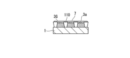
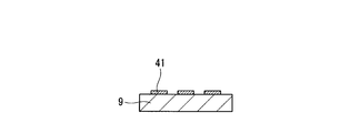
- FIG. 10 is a schematic cross-sectional view showing the manufacturing method of Comparative Example 1.
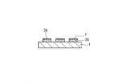
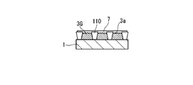
- FIG. 2 is a schematic cross-sectional view showing the manufacturing method of Example 1.
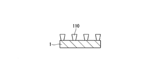
- FIG. 10 is a schematic cross-sectional view showing the production method of Example 2.
- FIG. 10 is a schematic cross-sectional view showing the production method of Example 2.
- FIG. 10 is a schematic cross-sectional view showing the production method of Example 2.
- FIG. 6 is a schematic cross-sectional view showing the production method of Example 3.
- FIG. 6 is a schematic cross-sectional view showing the production method of Example 3.
- FIG. 6 is a schematic cross-sectional view showing the production method of Example 3.
- FIG. 6 is a schematic cross-sectional view showing the production method of Example 3.
- FIG. 10 is a schematic cross-sectional view showing the production method of Example 3.
- FIG. 10 is a schematic cross-sectional view showing the manufacturing method of Comparative Example 2.
- FIG. 10 is a schematic cross-sectional view showing the manufacturing method of Comparative Example 2.
- FIG. 10 is a schematic cross-sectional view showing the manufacturing method of Comparative Example 2.
- FIG. 10 is a schematic cross-sectional view showing the manufacturing method of Comparative Example 2.
- FIG. 10 is a schematic cross-sectional view showing the manufacturing method of Comparative Example 2.
- FIG. 10 is a schematic cross-sectional view showing the production method of Example 4.
- FIG. 10 is a schematic cross-sectional view showing the production method of Example 4.
- FIG. 10 is a schematic cross-sectional view showing the production method of Example 5.
- FIG. 10 is a schematic cross-sectional view showing the production method of Example 5.
- FIG. 10 is a schematic cross-sectional view showing the production method of Example 5.
- FIG. 10 is a schematic cross-sectional view showing the production method of Example 5.
- FIG. 10 is a schematic cross-sectional view showing the production method of Example 5.
- FIG. 10 is a schematic cross-sectional view showing the production method of Example 5.
- FIG. 10 is a schematic cross-sectional view showing the production method of Example 5.
- FIG. 10 is a schematic cross-sectional view showing the production method of Example 5.
- FIG. 10 is a schematic cross-sectional view showing the production method of Example 5.
- FIG. 10 is a schematic cross-sectional view showing the production method of Example 5.
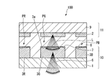
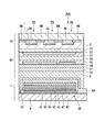
- FIG. 1 is a schematic cross-sectional view of a display device 100 according to the first embodiment.
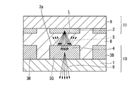
- FIG. 2 is a schematic cross-sectional view of a conventional display device.
- the display device 100 includes a phosphor substrate 10 and a light source 11 bonded to the phosphor substrate 10 via an adhesive layer 8.
- one pixel which is the minimum unit that constitutes an image, is configured by three dots that respectively perform red, green, and blue display.
- a dot that performs red display is referred to as a red pixel PR
- a dot that performs green display is referred to as a green pixel PG
- a dot that performs blue display is referred to as a blue pixel PB.
- ultraviolet light or blue light is emitted as the excitation light L from the light emitting element 2 of the light source 11.
- red fluorescence 6 is generated in the red pixel PR
- green fluorescence 6 is generated in the green pixel PG
- blue fluorescence 6 is generated in the blue pixel PB. Occurs. Then, full color display is performed by these three color lights of red, green and blue.
- a phosphor substrate 10 includes a substrate 1 and phosphor layers 3R, 3G, and 3B that are provided on the substrate 1 and generate fluorescence by excitation light L incident from the opposite side of the substrate 1. ing.
- the surface of the excitation light incident surface 3a on which the excitation light L of the phosphor layers 3R, 3G, 3B is incident is uneven, and the planarizing film 7 is provided on the excitation light incident surface 3a of the phosphor layers 3R, 3G, 3B. It has been.
- the excitation light incident surface 3a is a surface other than the surface where the phosphor layers 3R, 3G, and 3B are in contact with the substrate 1, and the surface on which the excitation light L emitted from the light emitting element 2 of the light source 11 can enter.
- the flattening film 7 is for flattening the surface of the excitation light incident surface 3a.
- the average surface roughness Ra of the surface of the planarizing film 7 opposite to the substrate 1 (surface facing the light source 11) is smaller than the average surface roughness Ra of the portion where the irregularities of the excitation light incident surface 3a are formed. .
- the average surface roughness Ra of the excitation light incident surface 3a is 1 ⁇ m or more and 10 ⁇ m or less, and the average surface roughness Ra of the surface of the planarizing film 7 opposite to the phosphor layers 3R, 3G, 3B is less than 1 ⁇ m. is there.
- the phosphor layers 3R, 3G, and 3B are composed of a plurality of phosphor layers divided for each dot.
- the plurality of phosphor layers 3R, 3G, and 3B are made of different phosphor materials in order to emit color light of different colors depending on the dots.
- the phosphor materials constituting the plurality of phosphor layers 3R, 3G, 3B may have different refractive indexes.
- the phosphor layers 3R, 3G, 3B are made of, for example, a thin film having a rectangular shape in plan view.
- a reflective member that reflects the fluorescent light 6 may be formed so as to cover a part or the entire circumference of the side surfaces of the phosphor layers 3R, 3G, and 3B.
- the wavelength selective transmission / reflection member that transmits the excitation light L and reflects the fluorescence emitted from the phosphor layers 3R, 3G, and 3B to the outer surface side of the excitation light incident surface 3a of the phosphor layers 3R, 3G, and 3B. Is preferably formed.
- the wavelength selective transmission / reflection member By providing the wavelength selective transmission / reflection member, the fluorescence emitted from the phosphor layers 3R, 3G, 3B is incident on the phosphor layers 3R, 3G, 3B again, and the light extraction efficiency can be increased.
- the wavelength selective transmission / reflection member may also serve as a planarization film.
- transmitting the excitation light means transmitting at least light corresponding to the peak wavelength of the excitation light.
- the reflection of the fluorescence generated in the phosphor layers 3R, 3G, 3B means that at least the light corresponding to each emission peak wavelength from the phosphor layers 7R, 7G, 7B is reflected.
- the refractive index of the layer (for example, the adhesive layer 8) in contact with the excitation light incident surface 3a of the phosphor layers 3R, 3G, 3B is higher than the refractive index of the phosphor layers 3R, 3G, 3B. .
- the excitation light 5 incident on the phosphor layers 3R, 3G, 3B is totally reflected.
- the excitation light component 4 that can enter the phosphor layers 3R, 3G, and 3B decreases, and the phosphor layers 3R, 3G, and 3B cannot be excited efficiently (broken arrows in FIG. 2).
- the refractive index of the layer for example, the adhesive layer 8 in contact with the excitation light incident surface 3a of the phosphor layers 3R, 3G, 3B is lower than the refractive index of the phosphor layers 3R, 3G, 3B, as described above. Total reflection does not occur. However, all of the excitation light 5 incident on the phosphor layers 3R, 3G, 3B at an angle of a certain angle or more is reflected on the excitation light incident surface 3a of the phosphor layers 3R, 3G, 3B.
- the excitation light component 4 that can enter the phosphor layers 3R, 3G, and 3B decreases, and the phosphor layers 3R, 3G, and 3B cannot be efficiently excited (broken lines in FIG. 2). Note that surface reflection is more likely to occur as the refractive index difference between the media increases and as the incident angle increases.
- the excitation light incidence of the phosphor layers 3R, 3G, 3B is performed.
- the incident angle of the excitation light L incident on the surface 3a tends to be relatively small. That is, the excitation light L easily enters the excitation light incident surface 3a of the phosphor layers 3R, 3G, and 3B below the critical angle at which total reflection occurs or below the incident angle at which surface reflection occurs. Therefore, the loss of the excitation light component incident on the phosphor layers 3R, 3G, 3B can be reduced, and the fluorescence components generated in the phosphor layers 3R, 3G, 3B can be increased.
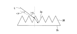
- FIG. 3A shows an example in which the excitation light incident surface 3a of the phosphor layer 3R is flat. It is assumed that the thickness of the phosphor layer 3R shown in FIG. 3A is uniform.
- the excitation light L is incident on the flat excitation light incident surface 3a at an angle larger than the critical angle ⁇ , the excitation light L is totally reflected on the surface of the phosphor layer 3R.
- the incident angle of the excitation light L (incident light) with respect to the bottom surface 3b of the phosphor layer 3R is the same as the excitation light L shown in FIG. 3A
- the incident angle of the excitation light L with respect to the excitation light incident surface 3a is equal to or less than the critical angle ⁇ . It becomes. Therefore, the excitation light L is incident on the phosphor layer 3R.
- the critical angle ⁇ with respect to the flat excitation light incident surface 3a is obtained.
- the excitation light L is incident at the following angle, the excitation light L is incident on the phosphor layer 3R.
- the incident angle of the excitation light L with respect to the bottom surface 3b of the phosphor layer 3R is the same as the excitation light L shown in FIG. 3C
- the incident angle of the excitation light L with respect to the excitation light incident surface 3a is not less than the critical angle ⁇ . Therefore, the excitation light L is totally reflected by the excitation light incident surface 3a. The totally reflected excitation light L reaches the excitation light incident surface 3a again.
- the incident angle of the excitation light L with respect to the excitation light incident surface 3a is equal to or smaller than the critical angle ⁇ and is incident on the phosphor layer 3R.
- the excitation light L is totally reflected by the excitation light incident surface 3a. Thereafter, the excitation light L that has reached the excitation light incident surface 3a again is totally reflected again at the excitation light incident surface 3a because the incident angle of the excitation light L with respect to the excitation light incident surface 3a is equal to or greater than the critical angle ⁇ .
- the totally reflected excitation light L reaches the excitation light incident surface 3a again and enters the excitation light incident surface 3a because the incident angle of the excitation light L with respect to the excitation light incident surface 3a is equal to or smaller than the critical angle ⁇ .
- 3D and 3E show an example in which the light enters the excitation light incident surface 3a after one total reflection or two total reflections of the excitation light L, but the present embodiment is not limited to this. Not.
- the excitation light L repeats total reflection several times at the excitation light incident surface 3a and the incident angle of the excitation light L with respect to the excitation light incident surface 3a becomes equal to or less than the critical angle ⁇ , the excitation light L is incident on the excitation light incident surface 3a.
- the phosphor layer 3R may be configured.
- the excitation light incident surfaces 3a of the phosphor layers 3R, 3G, and 3B are uneven, even if the incident angle of the excitation light L is wide, the excitation light L is the phosphor layer phosphor layer 3R. , 3G, 3B. Therefore, compared with the case where the excitation light incident surfaces 3a of the phosphor layers 3R, 3G, and 3B are flat, the amount of the excitation light L incident is increased and the extraction efficiency of the fluorescence 6 is improved.
- the planarizing film 7 is formed on the excitation light incident surface 3a of the phosphor layers 3R, 3G, 3B, the phosphor substrate 10 and the excitation light side substrate (substrate on which the light emitting element 2 is provided) 9 are provided. It is possible to prevent the light emitting element 2 from being damaged by the surface irregularity shape of the excitation light incident surface 3a of the phosphor layers 3R, 3G, 3B when bonding the layers. Further, the refractive index of the planarizing film 7 is between the refractive index of the phosphor layers 3R, 3G, 3B and the refractive index of the layer (for example, the adhesive layer 8) in contact with the planarizing film 7 on the excitation light incident surface 3a side.
- the adhesive layer 8 may also serve as the planarizing film 7.
- the refractive index of the adhesive layer 8 is between the refractive index of the phosphor layers 3R, 3G, and 3B and the refractive index of the layer of the light emitting element 2 that is in contact with the adhesive layer 8 on the excitation light incident surface side.
- the structural member and the formation method of the fluorescent substance substrate 10 concerning this embodiment are explained concretely, the structural member and the formation method of the fluorescent substance substrate 10 are not limited to this.
- substrate Since the substrate for the phosphor substrate 10 used in the present embodiment needs to take out the fluorescence 6 from the phosphor layers 3R, 3G, 3B to the outside, in the light emitting region of the phosphor layers 3R, 3G, 3B, It is necessary to transmit the fluorescence 6.
- the substrate for the phosphor substrate 10 include an inorganic material substrate made of glass, quartz, and the like, a plastic substrate made of polyethylene terephthalate, polycarbazole, polyimide, and the like, but this embodiment is limited to these substrates. It is not a thing.
- a plastic substrate since it becomes possible to form a bending part and a bending part without stress, it is preferable to use a plastic substrate.
- a substrate obtained by coating a plastic substrate with an inorganic material is more preferable from the viewpoint of improving gas barrier properties. As a result, it is possible to eliminate the deterioration of the organic EL due to the permeation of moisture that may occur when the plastic substrate is used as an organic EL substrate, for example.
- the phosphor layers 3R, 3G, and 3B of the present embodiment absorb excitation light L from the light emitting element 2 such as an ultraviolet light emitting organic EL element, a blue light emitting organic EL element, an ultraviolet light emitting LED, and a blue LED, and red, green, It is composed of a red phosphor layer 3R that emits blue light, a green phosphor layer 3G, and a blue phosphor layer 3B.
- the blue phosphor layer 3B is not provided, and the blue excitation light L may be emitted from the blue pixel PB.
- the blue phosphor layer 3B is not provided, and the directional excitation light L is scattered so as to be emitted as isotropic light.
- a simple light scattering layer may be applied.
- a phosphor layer that emits cyan light and yellow light to the pixels as necessary.
- the color reproduction range can be further expanded as compared with a display device using pixels that emit three primary colors of red, green, and blue.
- the phosphor layers 3R, 3G, and 3B may be composed of only the phosphor materials exemplified below, and may optionally contain additives and the like, and these materials are polymer materials (binding resins). Or the structure disperse
- a known phosphor material can be used as the phosphor material of the present embodiment.
- Such phosphor materials are classified into organic phosphor materials and inorganic phosphor materials, and specific examples of these compounds are shown below, but the phosphor materials are not limited to these materials. .
- Organic phosphor materials include blue fluorescent dyes, stilbenzene dyes: 1,4-bis (2-methylstyryl) benzene, trans-4,4′-diphenylstilbenzene, coumarin dyes: 7-hydroxy- 4-methylcoumarin and the like can be mentioned.
- a green fluorescent dye a coumarin dye: 2,3,5,6-1H, 4H-tetrahydro-8-trifluoromethylquinolidine (9,9a, 1-gh) coumarin (coumarin 153), 3- ( 2'-benzothiazolyl) -7-diethylaminocoumarin (coumarin 6), 3- (2'-benzoimidazolyl) -7-N, N-diethylaminocoumarin (coumarin 7), naphthalimide dyes: basic yellow 51, solvent yellow 11, Solvent yellow 116 etc. are mentioned.
- the red fluorescent dye includes cyanine dye: 4-dicyanomethylene-2-methyl-6- (p-dimethylaminostyryl) -4H-pyran, pyridine dye: 1-ethyl-2- [4- ( p-dimethylaminophenyl) -1,3-butadienyl] -pyridinium-perchlorate, and rhodamine dyes: rhodamine B, rhodamine 6G, rhodamine 3B, rhodamine 101, rhodamine 110, basic violet 11, sulforhodamine 101 and the like. .
- blue phosphors such as Sr 2 P 2 O 7 : Sn 4+ , Sr 4 Al 14 O 25 : Eu 2+ , BaMgAl 10 O 17 : Eu 2+ , SrGa 2 S 4 are used.
- Y 2 O 2 S Eu 3+ , YAlO 3 : Eu 3+ , Ca 2 Y 2 (SiO 4 ) 6 : Eu 3+ , LiY 9 (SiO 4 ) 6 O 2 : Eu 3+ , YVO 4 : Eu 3+ , CaS: Eu 3+ , Gd 2 O 3 : Eu 3+ , Gd 2 O 2 S: Eu 3+ , Y (P, V) O 4 : Eu 3+ , Mg 4 GeO 5.5 F: Mn 4+ , Mg 4 GeO 6 : Mn 4+ , K 5 Eu 2.5 (WO 4 ) 6.25 , Na 5 Eu 2.5 (WO 4 ) 6.25 , K 5 Eu 2.5 (MoO 4 ) 6.25 , Na 5 Eu 2.5 (MoO 4 ) 6.25 and the like.
- the inorganic phosphor may be subjected to a surface modification treatment as necessary.
- the surface modification treatment include chemical treatment using a silane coupling agent, physical treatment using addition of submicron-order fine particles, and combinations thereof.
- an inorganic material it is preferable to use an inorganic material.
- the average particle size (d 50 ) is preferably 0.5 ⁇ m to 50 ⁇ m. When the average particle size is 1 ⁇ m or less, the luminous efficiency of the phosphor is rapidly reduced. Moreover, when it is 50 ⁇ m or more, it becomes difficult to pattern at a high resolution.
- the phosphor layer is formed by using a phosphor layer forming coating solution obtained by dissolving and dispersing the phosphor material and the resin material in a solvent, using a spin coating method, a dipping method, a doctor blade method, a discharge coating method, a spraying method.
- Known wet processes such as coating methods such as coating methods, ink jet methods, letterpress printing methods, intaglio printing methods, screen printing methods, printing methods such as micro gravure coating methods, etc.
- It can be formed by a known dry process such as a vapor deposition method, molecular beam epitaxy (MBE) method, sputtering method, organic vapor deposition (OVPD) method, or a laser transfer method.
- the phosphor layers 3R, 3G, and 3B can be patterned by a photolithography method by using a photosensitive resin as the polymer resin.
- the photosensitive resin a photosensitive resin (photocurable resist material) having a reactive vinyl group such as an acrylic acid resin, a methacrylic acid resin, a polyvinyl cinnamate resin, or a hard rubber resin is used. It is possible to use one kind or a mixture of plural kinds. Also, wet processes such as the ink jet method, relief printing method, intaglio printing method, screen printing method, resistance heating vapor deposition method using shadow mask, electron beam (EB) vapor deposition method, molecular beam epitaxy (MBE) method, sputtering method It is also possible to directly pattern the phosphor material by a known dry process such as an organic vapor deposition (OVPD) method or a laser transfer method.
- OVPD organic vapor deposition
- the film thickness of the phosphor is usually about 100 nm to 100 ⁇ m, preferably 1 ⁇ m to 100 ⁇ m. If the film thickness is less than 100 nm, it is impossible to sufficiently absorb the light emitted from the light source, so that the light emission efficiency is lowered, and the color purity is lowered by mixing the required transmitted light with the transmitted light of the excitation light. Arise. Further, in order to increase the absorption of light emitted from the light source and reduce the transmitted light of the excitation light to such an extent that the color purity is not adversely affected, the film thickness is preferably 1 ⁇ m or more. Further, if the film thickness exceeds 100 ⁇ m, the light emitted from the light source is already sufficiently absorbed. Therefore, the efficiency is not increased but only the material is consumed, and the material cost is increased.
- the light scattering particles may be made of an organic material or an inorganic material, but may be made of an inorganic material. It is preferable. This makes it possible to diffuse or scatter light having directivity from the light emitting element 2 more isotropically and effectively. Further, by using an inorganic material, it is possible to provide a light scattering layer that is stable to light and heat.
- the light scattering particles have high transparency.
- the refractive index ratio with a resin material is contained in the numerical range mentioned above.
- the main component is an oxide of at least one metal selected from the group consisting of silicon, titanium, zirconium, aluminum, indium, zinc, tin, and antimony. Examples thereof include particles (fine particles).
- particles (inorganic fine particles) made of an inorganic material for example, silica beads (refractive index: 1.44), alumina beads (refractive index: 1.63), titanium oxide.
- examples thereof include beads (refractive index: anatase type: 2.50, rutile type: 2.70), zirconia oxide beads (refractive index: 2.05), and zinc oxide beads (refractive index: 2.00).
- particles (organic fine particles) made of an organic material are used as the light scattering particles, for example, polymethyl methacrylate beads (refractive index: 1.49), acrylic beads (refractive index: 1.50), acrylic- Styrene copolymer beads (refractive index: 1.54), melamine beads (refractive index: 1.57), high refractive index melamine beads (refractive index: 1.65), polycarbonate beads (refractive index: 1.57), Styrene beads (refractive index: 1.60), crosslinked polystyrene beads (refractive index: 1.61), polyvinyl chloride beads (refractive index: 1.60), benzoguanamine-melamine formaldehyde beads (refractive index: 1.68), Examples thereof include silicone beads (refractive index: 1.50).
- the resin material used by mixing with the above-described light scattering particles is preferably a translucent resin.
- the resin material include melamine resin (refractive index: 1.57), nylon (refractive index: 1.53), polystyrene (refractive index: 1.60), melamine beads (refractive index: 1.57).
- Polycarbonate (refractive index: 1.57), polyvinyl chloride (refractive index: 1.60), polyvinylidene chloride (refractive index: 1.61), polyvinyl acetate (refractive index: 1.46), polyethylene (refractive Ratio: 1.53), polymethyl methacrylate (refractive index: 1.49), poly MBS (refractive index: 1.54), medium density polyethylene (refractive index: 1.53), high density polyethylene (refractive index: 1.54), tetrafluoroethylene (refractive index: 1.35), polytrifluoroethylene chloride (refractive index: 1.42), polytetrafluoroethylene (refractive index: 1.35), and the like.
- a method for making the surface of the excitation light incident surface 3a of the phosphor layers 3R, 3G, 3B uneven it is preferable to perform a blast treatment.
- a blast treatment known drive blasting such as air blasting or sand blasting or wet blasting can be used.
- Other methods for making the surface of the excitation light incident surface 3a of the phosphor layers 3R, 3G, and 3B uneven are a wet etching process using acid, a dry etching process using plasma gas, and the like. This is not a limitation.
- the method of making the surface of the excitation light incident surface 3a of the phosphor layers 3R, 3G, and 3B uneven is not required to be a single one, and may be performed by combining two or more processes.
- the surface of the excitation light incident surface 3a of the phosphor layers 3R, 3G, and 3B is largely roughened by blasting, and then the etching process is performed to form the irregular shape on the surface of the excitation light incident surface 3a of the phosphor layers 3R, 3G, and 3B May be finely controlled.
- the uneven shape need not be a random shape, and may be a periodic structure.
- the average surface roughness Ra of the irregular shape on the surface of the excitation light incident surface 3a of the phosphor layers 3R, 3G, 3B is preferably 1 ⁇ m or more, more preferably 1 ⁇ m or more and 10 ⁇ m or less.
- the average surface roughness Ra is less than 1 ⁇ m, the uneven shape effect is not exhibited.
- the average surface roughness Ra is larger than 10 ⁇ m, it becomes difficult to cover the entire excitation light incident surface 3a of the phosphor layers 3R, 3G, and 3B with the planarizing film 7, and even if the entire excitation light incident surface 3a is covered.
- the average surface roughness Ra refers to the arithmetic average roughness measured based on the standard of JIS B 0601: 2001.
- the phosphor layers 3R, 3G, and 3B do not have to be a single layer, and may have a multilayer structure of two or more layers. At this time, it is only necessary that the surface irregularities be formed only on the excitation light incident outermost surface of at least the phosphor layers 3R, 3G, 3B.
- the planarizing film 7 used for the excitation light incident surface 3a of the phosphor layers 3R, 3G, 3B of the present embodiment can be formed using a known material.
- the planarizing film 7 include inorganic materials such as silicon oxide, silicon nitride, and tantalum oxide, and organic materials such as polyimide, acrylic resin, and resist material.
- the method for forming the planarizing film 7 include a dry process such as a CVD method and a vacuum deposition method, and a wet process such as a spin coat method.
- the present embodiment is not limited to these materials and the formation method.
- the planarizing film 7 may have a single layer structure or a multilayer structure.
- Color filter In the phosphor substrate 10 of the present embodiment, it is preferable to provide a color filter between the substrate 1 on the light extraction side and the phosphor layers 3R, 3G, 3B.
- a conventional color filter can be used as the color filter.
- the color filter by providing the color filter, the color purity of the red pixel PR, the green pixel PG, and the blue pixel PB can be increased, and the color reproduction range of the display device 100 can be expanded.
- the blue color filter facing the blue phosphor layer 3B, the green color filter facing the green phosphor layer 3G, and the red color filter facing the red phosphor layer 3R are phosphor layers 3R, 3G, Absorbs excitation light that excites 3B.
- the blue color filter, the green color filter, and the red color filter can prevent the excitation light L that is not absorbed and transmitted through the phosphor layers 3R, 3G, and 3B from leaking to the outside, the phosphor layer 3R. , 3G, 3B and the color purity of the light emission due to the color mixture by the excitation light L can be prevented.
- the light source 11 As the light source 11 for exciting the phosphor layers 3R, 3G, and 3B, ultraviolet light and blue light are preferable.
- ultraviolet LED, blue LED, ultraviolet light emitting inorganic EL, blue light emitting inorganic EL, ultraviolet light emitting organic EL, and blue light emitting organic light are used.
- EL etc. are mentioned, this embodiment is not limited to these light sources. Further, by directly switching these light sources, it is possible to control ON / OFF of light emission for displaying an image.
- a layer having a shutter function such as liquid crystal is arranged between the phosphor layers 3R, 3G, 3B and the light source 11, and the ON / OFF of the light emission can be controlled by controlling the layer. Is possible. It is also possible to control ON / OFF of both the light source 11 and the layer having a shutter function such as liquid crystal.
- the light source 11 known ultraviolet LEDs, blue LEDs, ultraviolet light emitting inorganic ELs, blue light emitting inorganic ELs, ultraviolet light emitting organic ELs, blue light emitting organic ELs and the like can be used. It can be produced by a known production method.
- the ultraviolet light preferably emits light having a main light emission peak of 360 nm to 410 nm, and the blue light preferably has light emission of a main light emission peak of 410 nm to 470 nm.
- the light source 11 desirably has directivity. Directivity refers to the property that the intensity of light varies depending on the direction. The directivity may be provided at the time when light enters the phosphor layer.
- the light source 11 desirably makes parallel light incident on the phosphor layer.
- the light-emitting element 2 that can be suitably used for the light source 11 will be described.
- an LED light emitting diode
- a known LED can be used as the LED.
- an ultraviolet light emitting inorganic LED and a blue light emitting inorganic LED are suitable.
- the LED 2A includes, for example, a first buffer layer 23, an n-type contact layer 24, a second n-type cladding layer 25, a first n-type cladding layer 26, an active layer 27, and a first p-type.
- a clad layer 28, a second p-type clad layer 29, a second buffer layer 30, a cathode 22, and an anode 21 are provided.
- the LED 2A has a first buffer layer 23, an n-type contact layer 24, a second n-type clad layer 25, a first n-type clad layer 26, an active layer 27, a first p-type clad on one surface of the substrate 9.
- a layer 28, a second p-type cladding layer 29, and a second buffer layer 30 are sequentially stacked.
- a cathode 22 is formed on the n-type contact layer 24.
- An anode 21 is formed on the second buffer layer 30.
- the specific structure of LED is not restricted to the above-mentioned thing.
- the active layer 27 is a layer that emits light by recombination of electrons and holes, and a known active layer material for LED can be used as the active layer material.
- a known active layer material for LED can be used as the active layer material.
- an active layer material for example, as an ultraviolet active layer material, AlGaN, InAlN, In a Al b Ga 1-ab N (0 ⁇ a, 0 ⁇ b, a + b ⁇ 1), blue active layer material In z Ga 1 -z N (0 ⁇ z ⁇ 1) and the like are exemplified, but the active layer material is not limited thereto.
- the active layer 27 a single quantum well structure or a multiple quantum well structure can be used.
- the active layer of the quantum well structure may be either n-type or p-type.
- the half-value width of the emission wavelength is narrowed by band-to-band emission, and light emission with good color purity can be obtained. Therefore, it is preferable.
- the active layer 27 may be doped with donor impurities and / or acceptor impurities. If the crystallinity of the active layer doped with impurities is the same as that of non-doped, doping with donor impurities can further increase the emission intensity between bands as compared with non-doped ones.
- the acceptor impurity is doped, the peak wavelength can be shifted to a lower energy side by about 0.5 eV than the peak wavelength of interband light emission, but the full width at half maximum is increased.
- both the acceptor impurity and the donor impurity are doped, the light emission intensity can be further increased as compared with the light emission intensity of the active layer doped only with the acceptor impurity.
- the conductivity type of the active layer is preferably doped with a donor impurity such as Si to be n-type.
- n-type cladding layers 25 and 26 known n-type cladding layer materials for LEDs can be used.
- the n-type cladding layer is composed of two layers of the first n-type cladding layer 26 and the second n-type cladding layer 25, but the n-type cladding layer may be a single layer, Three or more layers may be used.
- the n-type cladding layer By forming the n-type cladding layer with a material formed of an n-type semiconductor having a band gap energy larger than that of the active layer 27, a potential barrier against holes is formed between the n-type cladding layer and the active layer 27. Can be confined in the active layer.
- n-type cladding layers 25 and 26 can be formed by n-type Inx Ga1-x N (0 ⁇ x ⁇ 1), but the n-type cladding layers 25 and 26 are not limited to these. Absent.
- the p-type cladding layers 28 and 29 a known p-type cladding layer material for LED can be used.
- the p-type cladding layer is composed of two layers of the first p-type cladding layer 28 and the second p-type cladding layer 29, but the p-type cladding layer may be a single layer, Three or more layers may be used.
- the p-type cladding layer By configuring the p-type cladding layer with a material formed of a p-type semiconductor having a larger band gap energy than the active layer 27, a potential barrier against electrons is formed between the p-type cladding layer and the active layer 27, and the electrons are active. It becomes possible to confine in the layer 27.
- the p-type cladding layers 28 and 29 can be formed of Aly Ga1-y N (0 ⁇ y ⁇ 1), but the p-type cladding layers 28 and 29 are not limited to these.
- n-type contact layer 24 a known contact layer material for LED can be used.
- an n-type contact layer made of n-type GaN can be formed as a layer for forming an electrode (cathode 22) in contact with the n-type cladding layer.
- a p-type contact layer made of p-type GaN as a layer for forming the electrode (anode 21) in contact with the p-type cladding layer.
- this contact layer need not be formed if the second n-type cladding layer 25 and the second p-type cladding layer 29 are made of GaN.
- the second n-type and p-type cladding layers are not necessary. Can be used as a contact layer.
- a known film formation process for LED can be used, but the film formation process is not particularly limited thereto.
- a vapor phase growth method such as MOVPE (metal organic vapor phase epitaxy), MBE (molecular beam vapor phase epitaxy), HDVPE (hydride vapor phase epitaxy), for example, sapphire (C plane, A plane, R ), SiC (including 6H—SiC, 4H—SiC), spinel (MgAl 2 O 4 , especially its (111) plane), ZnO, Si, GaAs, or other oxide single crystal substrates (such as NGO)
- MOVPE metal organic vapor phase epitaxy
- MBE molecular beam vapor phase epitaxy
- HDVPE hydrogen vapor phase epitaxy
- sapphire C plane, A plane, R
- SiC including 6H—SiC, 4H—SiC
- spinel MgAl 2 O 4 , especially its (111) plane
- an organic EL element can be used as the light emitting element 2B.
- a known organic EL can be used.
- the organic EL element 2B includes, for example, an anode 41, a hole injection layer 43, a hole transport layer 44, a light emitting layer 45, a hole prevention layer 46, an electron transport layer 47, an electron on one surface of the substrate 9.
- An injection layer 48 and a cathode 49 are provided.
- the organic EL element 2B includes an anode 41, a hole injection layer 43, a hole transport layer 44, a light emitting layer 45, a hole prevention layer 46, an electron transport layer 47, and an electron injection layer on one surface of the substrate 9.
- the organic EL element 2B only needs to include an organic EL layer including at least a light emitting layer (organic light emitting layer) 45 made of an organic light emitting material between the anode 41 and the cathode 49.
- the specific configuration is as described above. It is not limited to. In the following description, the layers from the hole injection layer 14 to the electron injection layer 19 may be referred to as an organic EL layer.
- the organic EL element 2B is provided in a matrix corresponding to each of the red pixel PR, the green pixel PG, and the blue pixel PB shown in FIG. 1, and is individually controlled to be turned on / off.
- the driving method of the plurality of organic EL elements 2B may be active matrix driving or passive matrix driving. A configuration example using an active matrix organic EL element will be described in detail later.
- substrate As the substrate 9 used in this embodiment, for example, an inorganic substrate made of glass, quartz, etc., a plastic substrate made of polyethylene terephthalate, polycarbazole, polyimide, etc., an insulating substrate such as a ceramic substrate made of alumina, or the like, or A metal substrate made of aluminum (Al), iron (Fe), or the like, or a substrate in which an insulating material made of silicon oxide (SiO 2 ) or an organic insulating material is coated on the substrate, or a metal substrate made of Al or the like Examples thereof include a substrate whose surface is subjected to insulation treatment by a method such as anodization.
- a substrate in which the plastic substrate is coated with an inorganic material, and a substrate in which the metal substrate is coated with an inorganic insulating material are more preferable.
- the film thickness of the organic EL is very thin, about 100 nm to 200 nm, so that the current in the pixel portion due to the protrusions Leakage (short circuit) can be eliminated.
- a substrate that does not melt at a temperature of 500 ° C. or lower and does not cause distortion.
- a general metal substrate has a coefficient of thermal expansion different from that of glass, it is difficult to form a TFT on the metal substrate with a conventional production apparatus, but the linear expansion coefficient is 1 ⁇ 10 ⁇ 5 / ° C. or less.
- a metal substrate which is an iron-nickel alloy of this type and adjusting the linear expansion coefficient to glass, it becomes possible to form TFTs on the metal substrate at low cost using a conventional production apparatus.
- the heat resistant temperature is low, it is possible to transfer and form the TFT on the plastic substrate by forming the TFT on the glass substrate and then transferring the TFT to the plastic substrate.
- the substrate to be used is from the organic EL layer. It is necessary to use a transparent or translucent substrate in order to extract the emitted light.
- the anode 41 and the cathode 49 used in the present embodiment function as a first electrode and a second electrode that supply current to the organic EL layer.
- the anode 41, which is the first electrode is disposed on the substrate 9
- the cathode 49, which is the second electrode is disposed on the opposite side of the substrate 9 across the organic EL layer. It may be. That is, the anode 41 that is the first electrode may be disposed on the opposite side of the substrate 9 with the organic EL layer interposed therebetween, and the cathode 49 that is the second electrode may be disposed on the substrate 9.
- Specific compounds and formation methods are exemplified below, but the compounds and formation methods are not limited to these.
- an electrode material for forming the anode 41 and the cathode 49 a known electrode material can be used.
- an electrode material for forming the anode 41 gold (Au), platinum (Pt), nickel (Ni) or the like having a work function of 4.5 eV or more from the viewpoint of more efficiently injecting holes into the organic EL layer.
- metals such as barium (Ba) and aluminum (Al), or alloys such as Mg: Ag alloy and Li: Al alloy containing these metals.
- the anode 41 and the cathode 49 can be formed using the above materials by a known method such as an EB vapor deposition method, a sputtering method, an ion plating method, or a resistance heating vapor deposition method. Is not limited to these forming methods. If necessary, the formed electrode can be patterned by a photolithographic fee method or a laser peeling method, or a patterned electrode can be directly formed by combining with a shadow mask.
- the film thickness is preferably 50 nm or more. When the film thickness is less than 50 nm, the wiring resistance is increased, which may increase the drive voltage.
- a translucent electrode is used as the anode 41. It is preferable to use it.
- a material used here it is possible to use a metal translucent electrode alone or a combination of a metal translucent electrode and a transparent electrode material, but as a translucent electrode material, from the viewpoint of reflectance and transmittance Silver is preferred.
- the film thickness of the semitransparent electrode is preferably 5 nm to 30 nm. When the film thickness is less than 5 nm, light cannot be sufficiently reflected, and interference effects cannot be obtained sufficiently.
- the film thickness exceeds 30 nm, the light transmittance is drastically reduced, so that the luminance and efficiency may be lowered.
- an electrode with high reflectivity that reflects light as the cathode 49.
- electrode materials used in this case include reflective metal electrodes such as aluminum, silver, gold, aluminum-lithium alloys, aluminum-neodymium alloys, and aluminum-silicon alloys, transparent electrodes, and reflective metal electrodes (reflective electrodes). The electrode etc. which combined these are mentioned.
- the anode 41 When light emitted from the organic EL layer is taken out from the cathode 49 side, the anode 41 may be formed of a highly reflective electrode and the cathode 49 may be a translucent electrode, contrary to the above.
- Organic EL layer used in the present embodiment may be a single layer structure of an organic light emitting layer or a multilayer structure of an organic light emitting layer and a charge transport layer. Specifically, the following configurations may be mentioned. The configuration is not limited by these. In the example of FIG. 5, the following configuration (8) is used. In the following description, holes and electrons are referred to as charges, and a layer that injects charges from the anode 41 or the cathode 49 toward the light emitting layer 45 (hole injection layer or electron injection layer) is referred to as a charge injection layer.
- a layer (hole transport layer, electron transport layer) that transports charges injected from the anode 41 or the cathode 49 by the charge injection layer toward the light emitting layer 45 is referred to as a charge transport layer, and the charge injection layer and the charge transport layer are collectively referred to. Therefore, it may be referred to as a charge injection / transport layer.
- Organic light emitting layer (2) Hole transport layer / organic light emitting layer (3) Organic light emitting layer / electron transport layer (4) Hole transport layer / organic light emitting layer / electron transport layer (5) Hole injection layer / Hole transport layer / organic light emitting layer / electron transport layer (6) hole injection layer / hole transport layer / organic light emitting layer / electron transport layer / electron injection layer (7) hole injection layer / hole transport layer / organic Light emitting layer / Hole prevention layer / Electron transport layer (8) Hole injection layer / Hole transport layer / Organic light emitting layer / Hole prevention layer / Electron transport layer / Electron injection layer (9) Hole injection layer / Hole Transport layer / electron prevention layer / organic light emitting layer / hole prevention layer / electron transport layer / electron injection layer
- Each layer of the organic light emitting layer, hole injection layer, hole transport layer, hole prevention layer, electron prevention layer, electron transport layer and electron injection layer may have a single layer structure or a multilayer structure.
- the organic light emitting layer 45 may be composed of only an organic light emitting material exemplified below, or may be composed of a combination of a light emitting dopant and a host material, and optionally a hole transport material, an electron transport material, Additives (donor, acceptor, etc.) may be included, and these materials may be dispersed in a polymer material (binding resin) or an inorganic material. From the viewpoint of luminous efficiency and lifetime, it is preferable that a luminescent dopant is dispersed in the host material.
- organic light emitting material a known light emitting material for organic EL can be used. Such light-emitting materials are classified into low-molecular light-emitting materials, polymer light-emitting materials, and the like. Specific examples of these compounds are given below, but organic light-emitting materials are not limited to these materials.
- the light-emitting material may be classified into a fluorescent material, a phosphorescent material, and the like, and it is preferable to use a phosphorescent material with high light emission efficiency from the viewpoint of reducing power consumption.
- organic light emitting material is not limited to these materials.
- a known dopant material for organic EL can be used as the light-emitting dopant optionally contained in the light-emitting layer.
- a dopant material for example, as an ultraviolet light emitting material, p-quaterphenyl, 3,5,3,5 tetra-t-butylsecphenyl, 3,5,3,5 tetra-t-butyl-p -Fluorescent materials such as quinckphenyl.
- Fluorescent light emitting materials such as styryl derivatives, bis [(4,6-difluorophenyl) -pyridinato-N, C2 ′] picolinate, iridium (III) (FIrpic), bis (4 ′, 6′-difluorophenyl) And phosphorescent organometallic complexes such as polydinato) tetrakis (1-pyrazoyl) borate, iridium (III) (FIr6), and the like.
- a known host material for organic EL can be used as a host material when using a dopant.
- host materials include the low-molecular light-emitting materials, the polymer light-emitting materials, 4,4′-bis (carbazole) biphenyl, 9,9-di (4-dicarbazole-benzyl) fluorene (CPF), 3 , 6-bis (triphenylsilyl) carbazole (mCP), carbazole derivatives such as (PCF), aniline derivatives such as 4- (diphenylphosphoyl) -N, N-diphenylaniline (HM-A1), 1,3- And fluorene derivatives such as bis (9-phenyl-9H-fluoren-9-yl) benzene (mDPFB) and 1,4-bis (9-phenyl-9H-fluoren-9-yl) benzene (pDPFB).
- the charge injection / transport layer is used to more efficiently inject charges (holes, electrons) from the electrode and transport (injection) to the light emitting layer, and the charge injection layer (hole injection layer, electron injection layer). It is classified as a transport layer (hole transport layer, electron transport layer).
- the charge injecting and transporting layer may be composed only of the charge injecting and transporting material exemplified below, and may optionally contain additives (donor, acceptor, etc.), and these materials are polymer materials (conjugation). Wear resin) or a structure dispersed in an inorganic material.
- charge injection / transport material known charge transport materials for organic EL and organic photoconductors can be used. Such charge injecting and transporting materials are classified into hole injecting and transporting materials and electron injecting and transporting materials. Specific examples of these compounds are given below, but the charge injecting and transporting materials are not limited to these materials. Absent.
- hole injection and hole transport materials include oxides such as vanadium oxide (V 2 O 5 ) and molybdenum oxide (MoO 2 ), inorganic p-type semiconductor materials, porphyrin compounds, N, N′-bis (3 -Methylphenyl) -N, N′-bis (phenyl) -benzidine (TPD), N, N′-di (naphthalen-1-yl) -N, N′-diphenyl-benzidine (NPD), etc.
- oxides such as vanadium oxide (V 2 O 5 ) and molybdenum oxide (MoO 2 )
- inorganic p-type semiconductor materials such as silicon oxide (V 2 O 5 ) and molybdenum oxide (MoO 2 ), inorganic p-type semiconductor materials, porphyrin compounds, N, N′-bis (3 -Methylphenyl) -N, N′-bis (phenyl) -benzidine (TPD), N, N′-d
- Low molecular weight materials such as tertiary amine compounds, hydrazone compounds, quinacridone compounds, styrylamine compounds, polyaniline (PANI), polyaniline-camphor sulfonic acid (PANI-CSA), 3,4-polyethylenedioxythiophene / polystyrene sulfonate ( PEDOT / PSS), poly (triphenylamine) derivative (Poly-TPD), polyvinylcarbazole (PV Cz), poly (p-phenylene vinylene) (PPV), poly (p-naphthalene vinylene) (PNV) and the like.
- the highest occupied molecular orbital than the hole injection transport material used for the hole transport layer 44 is used as a material used as the hole injection layer 43 in terms of more efficiently injecting and transporting holes from the anode 41.
- a material having a low energy level of (HOMO) is preferably used, and a material having a higher hole mobility than the hole injection transport material used for the hole injection layer 43 is used as the hole transport layer 44. preferable.
- acceptor material In order to improve the hole injection and transport properties, it is preferable to dope the hole injection and transport material with an acceptor.
- an acceptor a known acceptor material for organic EL can be used. Although these specific compounds are illustrated below, acceptor material is not limited to these materials.
- Acceptor materials include Au, Pt, W, Ir, POCl 3 , AsF 6 , Cl, Br, I, vanadium oxide (V 2 O 5 ), molybdenum oxide (MoO 2 ), and other inorganic materials, TCNQ (7, 7 , 8,8, -tetracyanoquinodimethane), TCNQF 4 (tetrafluorotetracyanoquinodimethane), TCNE (tetracyanoethylene), HCNB (hexacyanobutadiene), DDQ (dicyclodicyanobenzoquinone), etc.
- TNF trinitrofluorenone
- DNF dinitrofluorenone
- organic materials such as fluoranyl, chloranil and bromanyl.
- compounds having a cyano group such as TCNQ, TCNQF 4 , TCNE, HCNB, DDQ and the like are more preferable because they can increase the carrier concentration more effectively.
- Examples of electron injection and electron transport materials include inorganic materials that are n-type semiconductors, oxadiazole derivatives, triazole derivatives, thiopyrazine dioxide derivatives, benzoquinone derivatives, naphthoquinone derivatives, anthraquinone derivatives, diphenoquinone derivatives, fluorenone derivatives, benzodifuran derivatives. And low molecular weight materials such as poly (oxadiazole) (Poly-OXZ) and polystyrene derivatives (PSS).
- examples of the electron injection material include fluorides such as lithium fluoride (LiF) and barium fluoride (BaF 2 ), and oxides such as lithium oxide (Li 2 O).
- the material used as the electron injection layer 48 is more efficient in injecting and transporting electrons from the cathode 49 than the electron injection and transport material used in the electron transport layer 47. It is preferable to use a material having a high electron mobility, and it is preferable to use a material having a higher electron mobility than the electron injection transport material used for the electron injection layer 48 as the material used for the electron transport layer 47.
- the electron injection and transport material In order to further improve the electron injection and transport properties, it is preferable to dope the electron injection and transport material with a donor.
- a donor a known donor material for organic EL can be used. Although these specific compounds are illustrated below, donor material is not limited to these materials.
- Donor materials include inorganic materials such as alkali metals, alkaline earth metals, rare earth elements, Al, Ag, Cu, In, anilines, phenylenediamines, benzidines (N, N, N ′, N′-tetraphenyl) Benzidine, N, N'-bis- (3-methylphenyl) -N, N'-bis- (phenyl) -benzidine, N, N'-di (naphthalen-1-yl) -N, N'-diphenyl- Benzidine, etc.), triphenylamines (triphenylamine, 4,4′4 ′′ -tris (N, N-diphenyl-amino) -triphenylamine, 4,4′4 ′′ -tris (N-3- Methylphenyl-N-phenyl-amino) -triphenylamine, 4,4′4 ′′ -tris (N- (1-naphthyl) -N
- organic materials such as condensed polycyclic compounds (wherein the condensed polycyclic compounds may have a substituent), TTFs (tetrathiafulvalene), dibenzofuran, phenothiazine, and carbazole.
- a compound having an aromatic tertiary amine as a skeleton, a condensed polycyclic compound, and an alkali metal are more preferable because the carrier concentration can be increased more effectively.
- the organic EL layers such as the light-emitting layer 45, the hole transport layer 44, the electron transport layer 47, the hole injection layer 43, and the electron injection layer 48 are organic EL layer forming coating solutions in which the above materials are dissolved and dispersed in a solvent.
- Coating methods such as spin coating method, dipping method, doctor blade method, discharge coating method, spray coating method, ink jet method, letterpress printing method, intaglio printing method, screen printing method, microgravure coating method, etc.
- a known wet process such as a resistance heating vapor deposition method, an electron beam (EB) vapor deposition method, a molecular beam epitaxy (MBE) method, a sputtering method, an organic vapor deposition (OVPD) method, etc., Alternatively, it can be formed by a laser transfer method or the like.
- the coating liquid for organic EL layer formation may contain the additive for adjusting the physical properties of coating liquid, such as a leveling agent and a viscosity modifier.
- the film thickness of each organic EL layer is usually about 1 nm to 1000 nm, but preferably 10 nm to 200 nm. If the film thickness is less than 10 nm, the properties (charge injection characteristics, transport characteristics, confinement characteristics) that are originally required cannot be obtained. In addition, pixel defects due to foreign matters such as dust may occur. On the other hand, if the film thickness exceeds 200 nm, the drive voltage increases due to the resistance component of the organic EL layer, leading to an increase in power consumption.
- an edge cover 42 is provided for the purpose of preventing leakage between the anode 41 and the cathode 49 at the edge portion of the anode 41 formed on the substrate 9 side.
- the edge cover 42 can be formed by a known method such as an EB vapor deposition method, a sputtering method, an ion plating method, or a resistance heating vapor deposition method using an insulating material, and a known dry or wet photolithography.
- the method of forming the edge cover 42 is not limited to these methods.
- a known material can be used as the material constituting the edge cover 42 and is not particularly limited in the present embodiment.
- the film thickness is preferably 100 nm to 2000 nm.
- the thickness is 100 nm or less, the insulating property is not sufficient, and leakage occurs between the anode 41 and the cathode 49, resulting in an increase in power consumption and non-light emission.
- the thickness is 2000 nm or more, the film forming process takes time, so that the productivity is lowered or the electrode is disconnected at the edge cover 42.
- the organic EL element 2B preferably has a microcavity structure (optical microresonator structure) due to an interference effect between a reflective electrode and a translucent electrode used as the anode 41 and the cathode 49, or a dielectric multilayer film.
- a microcavity structure optical microresonator structure
- the emission spectrum can be adjusted due to the interference effect, and the emission spectrum can be adjusted by adjusting to a desired emission peak wavelength and half width. Thereby, it is possible to control the phosphor layers 3R, 3G, and 3B to a spectrum that can be excited more effectively.
- Organic EL element 2B is electrically connected to an external drive circuit.
- the organic EL element 2B may be directly connected to and driven by an external drive circuit, or a switching circuit such as a TFT is arranged in the pixel, and the external drive circuit (scan line electrode) is connected to a wiring to which the TFT or the like is connected.
- Circuit source driver
- data signal electrode circuit gate driver
- power supply circuit may be electrically connected.
- FIG. 6 is a sectional view of an organic EL element substrate 70 (light source) using the active matrix driving type organic EL element 2B.
- the organic EL element substrate 70 of the present embodiment has a TFT (driving element) 51 formed on one surface of the substrate 9. That is, the gate electrode 52 and the gate line 53 are formed, and the gate insulating film 54 is formed on the substrate body 9 so as to cover the gate electrode 52 and the gate line 53.
- An active layer (not shown) is formed on the gate insulating film 54, and a source electrode 55, a drain electrode 56 and a data line 57 are formed on the active layer, and covers the source electrode 55, the drain electrode 56 and the data line 57.
- a planarizing film 58 is formed.
- planarization film 58 does not have to have a single layer structure, and may be configured by combining another interlayer insulating film and the planarization film. Further, a contact hole 59 that reaches the drain electrode 56 through the planarizing film or the interlayer insulating film is formed, and the organic EL element that is electrically connected to the drain electrode 56 through the contact hole 59 on the planarizing film 58. A 2B anode 41 is formed. The configuration of the organic EL element 2B itself is the same as that described above.
- the TFT 51 is formed on the substrate 9 before forming the organic EL element 2B, and functions as a pixel switching element and an organic EL element driving element.
- Examples of the TFT 51 used in this embodiment include known TFTs, which can be formed using known materials, structures, and formation methods.
- a metal-insulator-metal (MIM) diode can be used instead of the TFT 51.
- Examples of the material of the active layer of the TFT 51 include inorganic semiconductor materials such as amorphous silicon (amorphous silicon), polycrystalline silicon (polysilicon), microcrystalline silicon, and cadmium selenide, zinc oxide, indium oxide-gallium oxide, and the like. Examples thereof include oxide semiconductor materials such as zinc oxide, or organic semiconductor materials such as polythiophene derivatives, thiophene oligomers, poly (p-ferylene vinylene) derivatives, naphthacene, and pentacene. Further, as the structure of the TFT 51, for example, a staggered type, an inverted staggered type, a top gate type, a coplanar type, and the like can be given.
- a method for forming the active layer constituting the TFT 51 (1) a method of ion doping impurities into amorphous silicon formed by plasma induced chemical vapor deposition (PECVD), and (2) a silane (SiH 4 ) gas is used.
- PECVD plasma induced chemical vapor deposition
- SiH 4 silane
- amorphous silicon by low pressure chemical vapor deposition (LPCVD), crystallizing amorphous silicon by solid phase epitaxy to obtain polysilicon, and then ion doping by ion implantation, (3) Si 2 H A method in which amorphous silicon is formed by LPCVD using 6 gases or PECVD using SiH 4 gas, annealed by a laser such as an excimer laser, and amorphous silicon is crystallized to obtain polysilicon, followed by ion doping (Low temperature process), (4) LPCVD How is a polysilicon layer is formed by a PECVD method, a gate insulating film formed by thermal oxidation at 1000 ° C.
- LPCVD low pressure chemical vapor deposition
- the gate insulating film 54 of the TFT 51 used in this embodiment can be formed using a known material. Examples thereof include SiO 2 formed by PECVD, LPCVD, etc., or SiO 2 obtained by thermally oxidizing a polysilicon film. Further, the data line 57, the gate line 53, the source electrode 55, and the drain electrode 56 of the TFT 51 used in this embodiment can be formed using a known conductive material, for example, tantalum (Ta), aluminum (Al ), Copper (Cu), and the like.
- the TFT 51 according to this embodiment can be configured as described above, but is not limited to these materials, structures, and formation methods.
- the interlayer insulating film used in the present embodiment can be formed using a known material.
- the formation method include dry processes such as chemical vapor deposition (CVD) and vacuum deposition, and wet processes such as spin coating. Moreover, it can also pattern by the photolithographic method etc. as needed.
- the present embodiment is not limited to these materials and forming methods.
- unevenness is formed on the surface of the TFT 51 formed on the substrate 9, various wirings, and electrodes. Due to the unevenness, in the organic EL element 2B, for example, defects or disconnection of the anode 41 or the cathode 49, organic There is a possibility that the EL layer may be lost, the anode 41 and the cathode 49 may be short-circuited, or the withstand voltage may be reduced. Therefore, it is desirable to provide the planarization film 58 on the interlayer insulating film for the purpose of preventing these phenomena.
- the planarization film 58 used in the present embodiment can be formed using a known material, for example, an inorganic material such as silicon oxide, silicon nitride, or tantalum oxide, or an organic material such as polyimide, acrylic resin, or resist material. Etc.
- Examples of the method for forming the planarizing film 58 include a dry process such as a CVD method and a vacuum deposition method, and a wet process such as a spin coat method.
- the present embodiment is not limited to these materials and the formation method. .
- the planarizing film 58 may have a single layer structure or a multilayer structure.
- FIG. 7 is a schematic configuration diagram of a display device 100 including the organic EL element substrate 70.
- the display device 100 includes an organic EL element substrate 70, a phosphor substrate 10, a pixel unit 71, a gate signal side drive circuit 72, a data signal side drive circuit 73, a signal wiring 74, a current supply line 75, A flexible printed wiring board 76 (FPC) and an external drive circuit 77 are provided.
- the phosphor substrate 10 is disposed to face the organic EL element substrate 70.
- the pixel portion 71 is provided in a region where the organic EL element substrate 70 and the phosphor substrate 10 face each other.
- the gate signal side drive circuit 72, the data signal side drive circuit 73, the signal wiring 74, and the current supply line 75 supply a drive signal to the pixel portion 71.
- the flexible printed wiring board 76 is connected to the organic EL element substrate 70. *
- the organic EL element substrate 70 is connected to an external drive circuit 77 including a scanning line electrode circuit, a data signal electrode circuit, a power supply circuit, and the like via the FPC 76 in order to drive the organic EL element 2B shown in FIG. Are electrically connected.
- the switching circuit such as the TFT 51 shown in FIG. 6 is disposed in the pixel portion 71, and the organic EL element 2B is driven to the wiring such as the data line 57 and the gate line 53 to which the TFT 51 is connected.
- the data signal side driving circuit 73 and the gate signal side driving circuit 72 are connected to each other, and an external driving circuit 77 is connected to these driving circuits via a signal wiring 74.
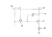
- a plurality of gate lines 53 and a plurality of data lines 57 are arranged, and TFTs 51 are arranged at intersections of the gate lines 53 and the data lines 57.
- the organic EL element according to the present embodiment is driven by a voltage-driven digital gradation method, and two TFTs, a switching TFT 60 and a driving TFT 51, are arranged for each pixel. And the anode of the light emitting portion (organic EL element 2B) are electrically connected through a contact hole 59 formed in the planarization layer 58 shown in FIG. Further, a capacitor 61 for setting the gate potential of the driving TFT 51 to a constant potential is arranged in one pixel so as to be connected to the gate electrode of the driving TFT 51.
- the present embodiment is not particularly limited to these, and the driving method may be the voltage-driven digital gradation method described above or the current-driven analog gradation method.
- the number of TFTs is not particularly limited, and the organic EL element may be driven by the two TFTs described above, and in order to prevent variations in TFT characteristics (mobility, threshold voltage), Alternatively, the organic EL element may be driven using two or more TFTs incorporating a compensation circuit.
- Reference numeral 62 indicates a power line.
- inorganic EL can be used as the light emitting element 2C.
- inorganic EL well-known inorganic EL can be used, for example, ultraviolet light emission inorganic EL and blue light emission inorganic EL are suitable.
- These inorganic EL elements are, for example, a light emitting element having a configuration in which a first electrode 81, a first dielectric layer 82, a light emitting layer 83, a second dielectric layer 84, and a second electrode 85 are sequentially stacked on one surface of a substrate 9. 2C.
- the specific configuration of the inorganic EL is not limited to the above.
- first electrode 81 and the second electrode 85 used in this embodiment metals such as aluminum (Al), gold (Au), platinum (Pt), nickel (Ni), and indium (In) and tin (
- transparent electrode material examples include an oxide (ITO) made of Sn), an oxide of Sn (Sn) (SnO 2 ), an oxide made of indium (In) and zinc (Zn) (IZO), etc. It is not limited to these materials. However, a transparent electrode such as ITO is better in the light extraction direction. A reflective film such as aluminum is preferably used on the side opposite to the light extraction direction.
- the first electrode 81 and the second electrode 85 can be formed by a known method such as an EB vapor deposition method, a sputtering method, an ion plating method, or a resistance heating vapor deposition method using the above materials. Is not limited to these forming methods. If necessary, the formed electrode can be patterned by a photolithographic fee method or a laser peeling method, or a patterned electrode can be directly formed by combining with a shadow mask.
- the film thickness is preferably 50 nm or more. When the film thickness is less than 50 nm, the wiring resistance is increased, which may increase the drive voltage.
- Dielectric layer As the first dielectric layer 82 and the second dielectric layer 84 used in the present embodiment, a known dielectric material for inorganic EL can be used. Examples of such dielectric materials include tantalum pentoxide (Ta 2 O 5 ), silicon oxide (SiO 2 ), silicon nitride (Si 3 N 4 ), aluminum oxide (Al 2 O 3 ), aluminum titanate ( AlTiO 3 ) barium titanate (BaTiO 3 ), strontium titanate (SrTiO 3 ) and the like can be mentioned, but the dielectric material is not limited to these.
- first dielectric layer 82 and the second dielectric layer 84 of the present embodiment may have one type selected from the above dielectric materials or a structure in which two or more types of materials are laminated.
- the film thicknesses of the first dielectric layer 82 and the second dielectric layer 84 are preferably about 200 nm to 500 nm.
- Light emitting layer As the light emitting layer 83 used in the present embodiment, a known light emitting material for inorganic EL can be used. As such a light emitting material, for example, ZnF 2 : Gd as an ultraviolet light emitting material, BaAl 2 S 4 : Eu, CaAl 2 S 4 : Eu, ZnAl 2 S 4 : Eu, Ba 2 as a blue light emitting material. Examples include SiS 4 : Ce, ZnS: Tm, SrS: Ce, SrS: Cu, CaS: Pb, (Ba, Mg) Al 2 S 4 : Eu, and the like, but the light emitting material is not limited thereto.
- the thickness of the light emitting layer 83 is preferably about 300 nm to 1000 nm.
- an LED, an organic EL element, an inorganic EL, or the like can be suitably used as the light emitting element 2 in FIG.
- a sealing film or a sealing substrate for sealing a light emitting element such as an LED, an organic EL element, and an inorganic EL.
- the sealing film and the sealing substrate can be formed by a known sealing material and sealing method.
- the sealing film can be formed by applying a resin on the surface opposite to the substrate main body constituting the light source by using a spin coat method, an ODF, or a laminate method.
- resin is further applied using spin coating, ODF, or lamination.
- the sealing film can be formed by bonding.
- Such a sealing film or sealing substrate can prevent the entry of oxygen and moisture into the light emitting element 2 from the outside, and the life of the light source 11 is improved. Further, when the light source 11 and the phosphor substrate 10 are bonded, it is possible to bond them with an adhesive layer 8 such as a general ultraviolet curable resin or a thermosetting resin. Further, when the light source 11 is directly formed on the phosphor substrate 10, for example, a method of sealing an inert gas such as nitrogen gas or argon gas with a glass plate, a metal plate, or the like can be given. Furthermore, it is preferable to mix a hygroscopic agent such as barium oxide in the enclosed inert gas because deterioration of the organic EL due to moisture can be more effectively reduced. However, this embodiment is not limited to these members and forming methods. When light is extracted from the side opposite to the substrate 1, it is necessary to use a light transmissive material for both the sealing film and the sealing substrate.
- an adhesive layer 8 such as a general ultraviolet curable resin or
- a polarizing plate on the light extraction side.
- the polarizing plate a combination of a conventional linear polarizing plate and a ⁇ / 4 plate can be used.
- the polarizing plate it is possible to prevent external light reflection from the electrodes of the display device 100 and external light reflection from the surface of the substrates 1 and 9 or the sealing substrate. Can be improved.
- FIG. 10 is a schematic cross-sectional view of the display device 200 of the second embodiment.
- the display device 200 is a configuration example in which a liquid crystal element 90 that is an optical member is inserted between the phosphor substrate 10 and the light source 11.
- components common to the display device 200 of the first embodiment are denoted by the same reference numerals, and detailed description thereof is omitted.
- the display device 200 of the present embodiment includes a phosphor substrate 10, an organic EL element substrate 11 (light source), and a liquid crystal element 90.
- the configuration of the phosphor substrate 10 is the same as that of the first embodiment, but only the point that the light absorption layer BM is provided along the boundary portion of each dot (red pixel PR, green pixel G, blue pixel PB). Is different.
- the laminated structure of the organic EL element substrate 11 is the same as that shown in FIG. 5 in the first embodiment.
- driving signals are individually supplied to the organic EL elements corresponding to the respective pixels, and each organic EL element is independently controlled to emit or not emit light.
- the organic EL element 2B is not divided for each pixel, and functions as a planar light source common to all the pixels.
- the liquid crystal element 90 is configured such that the voltage applied to the liquid crystal layer 98 can be controlled for each pixel using the pair of electrodes 93 and 94, and the transmittance of light emitted from the entire surface of the organic EL element 2B is set to the pixel. Control every time. That is, the liquid crystal element 90 has a function as an optical shutter that selectively transmits light from the organic EL element substrate 11 for each pixel.
- a known liquid crystal element can be used as the liquid crystal element 90 of the present embodiment.
- the liquid crystal element 90 includes a pair of polarizing plates 91 and 92, electrodes 93 and 94, alignment films 95 and 96, and a substrate 97.
- the liquid crystal 98 is sandwiched between the alignment films 95 and 96.
- one optically anisotropic layer is disposed between the liquid crystal cell and one polarizing plate 91 or 92, or the optically anisotropic layer is disposed between the liquid crystal cell and both polarizing plates 91 and 92. 2 may be arranged.
- the type of liquid crystal cell is not particularly limited and may be appropriately selected depending on the purpose. Examples thereof include TN mode, VA mode, OCB mode, IPS mode, and ECB mode.
- the liquid crystal element 90 may be passively driven or may be actively driven using a switching element such as a TFT.
- the phosphor substrate 10, the liquid crystal element 90, and the light source 11 are joined and integrated through the adhesive layer 8. That is, the surface of the phosphor substrate 10 on which the phosphor layers 3R, 3G, and 3B are formed and the polarizing plate 91 of the liquid crystal element 90 are bonded together via the adhesive layer 8 to form the organic EL element 2B of the light source 11. The surface and the polarizing plate 92 of the liquid crystal element 90 are bonded to each other with the adhesive layer 8 interposed therebetween.
- a mobile phone shown in FIG. 11A, a television receiver shown in FIG. 11B, and the like can be given.
- a cellular phone 1000 illustrated in FIG. 11A includes a main body 1001, a display unit 1002, a voice input unit 1003, a voice output unit 1004, an antenna 1005, an operation switch 1006, and the like.
- the display unit 1002 uses the display device of the above embodiment. It has been.
- a television receiver 1100 illustrated in FIG. 11B includes a main body cabinet 1101, a display portion 1102, a speaker 1103, a stand 1104, and the like, and the display device of the above embodiment is used for the display portion 1102. In such an electronic device, since the display device of the above-described embodiment is used, an electronic device with low power consumption and excellent display quality can be realized.
- a green phosphor layer 3G having a film thickness of 50 ⁇ m was formed on the substrate 1.
- the green phosphor layer 3G is formed by first adding 30 g of a green phosphor Ba 2 SiO 4 : Eu 2+ having an average particle diameter of 4 ⁇ m and 30 g of a 10 wt% aqueous solution of polyvinyl alcohol, and stirring the green phosphor.
- a coating solution was prepared.
- the green phosphor-forming coating solution produced as described above was pattern-coated on the glass at a width of 100 ⁇ m and a pitch of 160 ⁇ m by screen printing.
- the luminance of this phosphor substrate at 25 ° C. with 450 nm light was measured using a commercially available luminance meter (BM-7: manufactured by Topcontec House Co., Ltd.) as a blue LED as excitation light.
- BM-7 manufactured by Topcontec House Co., Ltd.
- Example 1 [The surface of the excitation light incident surface of the phosphor layer is made uneven] As shown in FIG. 13, like the comparative example 1, after producing the phosphor substrate in which the green phosphor layer 3G is patterned, the excitation light incident surface 3a of the phosphor layer 3G is used by using a sandblasting device, A fine powder of alumina having an average particle diameter of 4 ⁇ m is sprayed, and sand blasting is performed so that the average surface roughness Ra of the excitation light incident surface 3a of the phosphor layer 3G is 2 ⁇ m. The obtained green phosphor layer 3G was obtained.
- an acrylic photosensitive resin was patterned on the phosphor layer 3G by a photolithography technique to obtain a planarizing film 7.
- Example 2 [Adoption of side scattering film] As shown in FIG. 14A, a glass substrate was used as the substrate 1 as in Example 1. Next, a white resist pattern was formed in a forward taper shape with a 70 ⁇ m frame, a film thickness of 60 ⁇ m, and a pitch of 160 ⁇ m on the substrate 1 to produce a barrier 110 for partitioning dots.
- a green phosphor layer 3G dispenser technique was used to form a film having a thickness of 55 ⁇ m in the region partitioned by the barrier 110.
- the excitation light incident surface 3a of the phosphor layer 3G is injected with fine powder of alumina having an average particle diameter of 5 ⁇ m by using a wet blast device, and the excitation light incident on the phosphor layer 3G is incident.
- Wet blasting was performed so that the average surface roughness Ra of the surface 3a was 2 ⁇ m, thereby obtaining a green phosphor layer 3G having an uneven surface shape on the excitation light incident surface 3a.
- acrylic resin is fluorescent with a thickness of 20 ⁇ m by spin coating.
- the flattening layer 7 was formed by forming on the entire surface of the body substrate and heating at 120 ° C. for 30 minutes.
- Example 2 Since the light emission from the phosphor layer is isotropic, the fluorescent component directed to the side of the phosphor layer is lost in Example 1.
- the fluorescent component directed to the side of the phosphor layer is scattered by the barrier 110 and returns to the phosphor layer 3G so that it can be reused in the light extraction direction. That is, the barrier 110 functions as a reflecting member that reflects the fluorescence generated in the phosphor layer. Therefore, it can be considered that the luminance can be further improved as compared with Example 1 by adopting the structure as in Example 2.
- the barrier 110 may be a metal such as silver or aluminum that uses light reflection instead of light scattering. Further, the barrier 110 does not need to be made of a light scattering or light reflecting material, and it is sufficient that a light scattering or light reflecting film is formed at least on the surface of the barrier 110.
- Example 3 [Adoption of side scattering + backside wavelength selective transmission / reflection film] As shown in FIG. 15A, a glass substrate was used as the substrate 1 as in Example 1. Next, a white resist pattern was formed in a forward taper shape with a 70 ⁇ m frame, a film thickness of 60 ⁇ m, and a pitch of 160 ⁇ m on the substrate 1 to produce a barrier 110 for partitioning dots.
- a green phosphor layer 3G dispenser technique was used to form a film thickness of 55 ⁇ m between the barriers 110.
- the excitation light incident surface 3a of the phosphor layer 3G is ejected with fine powder of alumina having an average particle diameter of 4 ⁇ m using a sandblasting device, and the excitation light incident surface of the phosphor layer 3G is injected.
- Sand blasting was performed so that the average surface roughness Ra of 3G was 2 ⁇ m, and a green phosphor layer 3G having an uneven surface shape on the excitation light incident surface 3a was obtained.
- titanium oxide TiO2: refraction
- TiO2 refraction
- the wavelength selective transmission / reflection flattening film 7 functions as a wavelength selective transmission / reflection member that transmits excitation light and reflects fluorescence generated in the phosphor layer, and is formed by unevenness on the surface of the excitation light incident surface of the phosphor layer. It functions as a flattening film for flattening unevenness on the substrate.
- Example 3 Since the light emission from the phosphor layer 3G is isotropic, the fluorescent component toward the rear surface of the phosphor layer (the light incident surface of the phosphor layer) is lost in the second embodiment.
- the fluorescent component toward the rear surface of the phosphor layer is returned to the phosphor layer 3G by the wavelength selective transmission / reflection flattening film 7 and can be reused in the light extraction direction. Therefore, it can be considered that the luminance can be further improved as compared with Example 2 by adopting the structure as in Example 3. Since the wavelength selective transmission / reflection flattening film 7 does not transmit 100% of blue light of 450 nm, it also has a function as a light emission threshold filter of the phosphor layer 3G, and improves the contrast of the display device. Can also bear.
- a green phosphor layer 3G having a film thickness of 50 ⁇ m was formed on the substrate 1.
- the green phosphor layer 3G is formed by first adding 30 g of a green phosphor Ba 2 SiO 4 : Eu 2+ having an average particle diameter of 4 ⁇ m and 30 g of a 10 wt% aqueous solution of polyvinyl alcohol, and stirring the green phosphor. A coating solution was prepared. The green phosphor-forming coating liquid prepared above was applied onto the entire surface of the glass with a slit coater device.
- the excitation light incident surface 3a of the phosphor layer 3G is changed to a sandblasting device. Is used, and an alumina fine powder having an average particle diameter of 25 ⁇ m is sprayed, and sandblasting is performed so that the average surface roughness Ra of the excitation light incident surface 3a of the phosphor layer 3G is 15 ⁇ m. A green phosphor layer 3G having an uneven surface was obtained.
- a reflective electrode is formed by sputtering silver so as to have a thickness of 100 nm, and an indium-tin oxide (ITO) is formed thereon. ) was formed by sputtering to a film thickness of 20 nm.
- ITO indium-tin oxide
- the laminated film of the reflective electrode and the transparent electrode was patterned by a conventional photolithography method to obtain a first electrode 22 patterned in a stripe shape with an electrode width of 70 ⁇ m and a pitch of 160 ⁇ m.
- a patterned edge cover 23 is formed by conventional photolithography so as to cover only the edge portion of the first electrode 22. did.
- a short side of 5 ⁇ m from the end of the first electrode 22 is covered with SiO 2 .
- the substrate 21 is fixed to the substrate holder in the resistance heating vapor deposition apparatus, the pressure is reduced to a vacuum of 1 ⁇ 10 ⁇ 4 Pa or less, and the organic EL layer 24 including the organic light emitting layer is resistance heated. It formed by the vapor deposition method.
- TAPC 1,1-bis-di-4-tolylamino-phenyl-cyclohexane
- a hole injection layer having a thickness of 100 nm was formed by resistance heating vapor deposition.
- N, N′-di-1-naphthyl-N, N′-diphenyl-1,1′-biphenyl-1,1′-biphenyl-4,4′-diamine (NPD) is used as a hole transport material.
- a hole transport layer having a thickness of 40 nm was formed by resistance heating vapor deposition.
- This blue organic light-emitting layer comprises 1,4-bis-triphenylsilyl-benzene (UGH-2) (host material) and bis [(4,6-difluorophenyl) -pyridinato-N, C2 ′] picolinate iridium (III ) (FIrpic) (blue phosphorescent dopant) was prepared by co-evaporation at a deposition rate of 1.5 ⁇ / sec and 0.2 ⁇ / sec.
- UH-2 1,4-bis-triphenylsilyl-benzene
- FIrpic picolinate iridium
- a hole blocking layer (thickness: 10 nm) was formed on the light emitting layer using 2,9-dimethyl-4,7-diphenyl-1,10-phenanthroline (BCP).
- an electron transport layer (thickness: 30 nm) was formed on the hole blocking layer using tris (8-hydroxyquinoline) aluminum (Alq 3 ).
- an electron injection layer (thickness: 0.5 nm) was formed on the electron transport layer using lithium fluoride (LiF).
- a semitransparent electrode was formed as the second electrode 25.
- the substrate 9 is fixed to a metal deposition chamber.
- a shadow mask for forming the second electrode 25 (a mask having an opening so that the second electrode 25 can be formed in a stripe shape having a width of 70 ⁇ m and a pitch of 160 ⁇ m in a direction opposite to the stripe of the first electrode 41. )
- the substrate 21, and the surface of the electron injection layer is co-deposited with magnesium and silver at a deposition rate of 0.1 ⁇ / sec and 0.9 ⁇ / sec, respectively, by a vacuum evaporation method to form magnesium silver in a desired pattern. Formation (thickness: 1 nm).
- silver is formed in a desired pattern at a deposition rate of 1 mm / sec (thickness: 19 nm) for the purpose of emphasizing the interference effect and preventing voltage drop due to wiring resistance at the second electrode 25. did. Thereby, the second electrode 25 was formed.
- a microcavity effect (interference effect) appears between the reflective electrode (first electrode 22) and the semi-transmissive electrode (second electrode 25), and the front luminance can be increased.
- Light emission energy from the EL element can be more efficiently propagated to the phosphor layer.
- the emission peak was adjusted to 460 nm and the half-value width to 50 nm by the microcavity effect.
- an inorganic protective layer made of SiO 2 having a thickness of 3 ⁇ m was formed by patterning from the edge of the display portion to a sealing area of 2 mm in the vertical and horizontal directions by a plasma CVD method (not shown).
- the organic EL element substrate and the phosphor substrate produced as described above were aligned using an alignment marker formed outside the display unit.
- the phosphor substrate is previously coated with a thermosetting resin that also functions as a flattening film for relaxing the surface unevenness of the excitation light incident surface 3a of the phosphor layer. Both substrates were brought into intimate contact with each other and cured by heating at 80 ° C. for 2 hours.
- the above bonding step was performed in a dry air environment (water content: ⁇ 80 ° C.) for the purpose of preventing deterioration of the organic EL due to water.
- the organic EL display device was completed by connecting the terminals formed in the periphery to an external power source.
- the blue light-emitting organic EL is used as an excitation light source that can be arbitrarily switched, and the green phosphor layer converts the light emitted from the blue light to green.
- isotropic light emission was obtained, innumerable dark spots were generated on the display surface, resulting in a display with low luminance. This is because the surface irregularity of the excitation light incident surface 3a of the phosphor layer is as large as 15 ⁇ m, the flattening function of the thermosetting resin is not sufficient, and the second electrode 25 on the organic EL element substrate side is damaged at the time of bonding. It is thought that it was because it received.
- Example 4 [Blue organic EL + phosphor method] As shown in FIG. 18A, 0.7 mm of glass was used as the substrate 1. After washing with water, pure water ultrasonic cleaning 10 minutes, acetone ultrasonic cleaning 10 minutes, and isopropyl alcohol vapor cleaning 5 minutes were performed, followed by drying at 100 ° C. for 1 hour.
- a green phosphor layer 3G having a film thickness of 50 ⁇ m was formed on the substrate 1.
- the green phosphor layer 3G is formed by first adding 30 g of a green phosphor Ba 2 SiO 4 : Eu 2+ having an average particle diameter of 4 ⁇ m and 30 g of a 10 wt% aqueous solution of polyvinyl alcohol, and stirring the green phosphor. A coating solution was prepared. The green phosphor-forming coating liquid prepared above was applied onto the entire surface of the glass with a slit coater device.
- the excitation light incident surface 3a of the phosphor layer 3G is sandblasted.
- alumina fine powder having an average particle diameter of 20 ⁇ m is sprayed, and sand blasting is performed so that the average surface roughness Ra of the excitation light incident surface 3a of the phosphor layer 3G becomes 10 ⁇ m, and the excitation light incident surface 3a.
- a green phosphor layer 3G having an uneven surface was obtained.
- the organic EL element substrate and the phosphor substrate produced as described above were aligned using an alignment marker formed outside the display unit.
- the phosphor substrate is previously coated with a thermosetting resin that also functions as a flattening film for relaxing the surface unevenness of the excitation light incident surface 3a of the phosphor layer. Both substrates were brought into intimate contact with each other and cured by heating at 80 ° C. for 2 hours.
- the above bonding step was performed in a dry air environment (water content: ⁇ 80 ° C.) for the purpose of preventing deterioration of the organic EL due to water.
- the organic EL display device was completed by connecting the terminals formed in the periphery to an external power source.
- the blue light-emitting organic EL is used as an excitation light source that can be arbitrarily switched, and the green phosphor layer converts the light emitted from the blue light to green. Isotropic luminescence was obtained. Also, the dark spots on the display surface remained at two places. Moreover, it turned out that the luminance conversion efficiency from the blue light of Example 4 to the green light of Example 4 is improving about 3 times with respect to the luminance conversion efficiency from the blue light of Comparative Example 2.
- Example 5 [Blue organic EL + phosphor method] As shown in FIG. 19A, a 0.7 mm thick glass substrate is used as the substrate 1, and a silver paste is formed on the substrate 1 with a width of 70 ⁇ m, a film thickness of 60 ⁇ m, and a forward taper shape at a pitch of 160 ⁇ m by a screen printing method. A barrier 110 for partitioning dots was produced.
- the barrier 110 is a light-reflective barrier (hereinafter referred to as a reflection barrier) that reflects fluorescence generated in the phosphor layer.
- a red phosphor layer 3R, a green phosphor layer 3G, and a blue light scattering layer 115 are formed in a pattern in a region partitioned by the reflection barrier 110.
- red phosphor layer 3R In the formation process of the red phosphor layer 3R, 30 g of 10 wt% polyvinyl alcohol aqueous solution is added to 30 g of red phosphor K 5 Eu 2.5 (WO 4 ) 6.25 having an average particle size of 4 ⁇ m, and the mixture is stirred by a disperser. A coating solution was prepared. The prepared red phosphor forming coating solution was applied in a pattern to a region partitioned by the reflective barrier 110 by a dispenser technique. Subsequently, it was dried by heating in a vacuum oven (200 ° C., 10 mmHg) for 4 hours, and the red phosphor layer 3R was patterned with a film thickness of 55 ⁇ m (FIG. 19B).
- the green phosphor layer 3G In the formation process of the green phosphor layer 3G, 30 g of a 10 wt% polyvinyl alcohol aqueous solution was added to 30 g of the green phosphor Ba 2 SiO 4 : Eu 2+ having an average particle diameter of 4 ⁇ m, and the mixture was stirred by a disperser. A liquid was prepared. The green phosphor-forming coating liquid prepared as described above was applied in a pattern to a region partitioned by the reflective barrier 110 by a dispenser technique. Subsequently, it was dried by heating in a vacuum oven (200 ° C., 10 mmHg) for 4 hours to form a green phosphor layer 3G with a film thickness of 55 ⁇ m (FIG. 19C).
- the blue light scattering layer 115 In the step of forming the blue light scattering layer 115, 30 g of a 10 wt% polyvinyl alcohol aqueous solution is added to 30 g of 1.5 ⁇ m silica particles (refractive index: 1.65) and stirred with a disperser to form a blue scatterer layer forming coating solution.
- the blue scatterer layer-forming coating liquid prepared as described above was applied in a pattern to a region partitioned by the reflection barrier 110 by a dispenser technique. Subsequently, it was dried by heating in a vacuum oven (200 ° C., 10 mmHg) for 4 hours to form a blue light scattering layer 115 with a film thickness of 55 ⁇ m (FIG. 19D).
- the excitation light incident surface 3a of the green phosphor layer 3G and the red phosphor layer 3R and the excitation light incident surface 115a of the blue light scattering layer 115 are averaged by using a sandblast device.
- a fine powder of alumina having a diameter of 4 ⁇ m is sprayed, and sandblasting is performed so that the average surface roughness Ra of each excitation light incident surface of the green phosphor layer 3G, the red phosphor layer 3R, and the blue light scattering layer 115 is 2 ⁇ m.
- a green phosphor layer 3G, a red phosphor layer 3R, and a blue light scattering layer 115 having an uneven surface on the excitation light incident surface were obtained.
- a reflective electrode is formed by sputtering silver so as to have a thickness of 100 nm, and an indium-tin oxide (ITO) is formed thereon.
- ITO indium-tin oxide
- the laminated film of the reflective electrode and the transparent electrode was patterned by a conventional photolithography method to obtain the first electrode 41 patterned in a stripe shape with an electrode width of 70 ⁇ m and a pitch of 160 ⁇ m.
- SiO 2 is deposited to 200 nm on the substrate 9 by sputtering, and the edge cover 42 is patterned by a conventional photolithography method so as to cover only the edge portion of the first electrode 41. Formed.
- the short side is covered with SiO 2 by 5 ⁇ m from the end of the first electrode 41. This was washed with water, then subjected to pure water ultrasonic cleaning for 10 minutes, acetone ultrasonic cleaning for 10 minutes, and isopropyl alcohol vapor cleaning for 5 minutes, and dried at 120 ° C. for 1 hour.
- the substrate 9 is fixed to the substrate holder in the resistance heating vapor deposition apparatus, the pressure is reduced to a vacuum of 1 ⁇ 10 ⁇ 4 Pa or less, and the organic EL layer 120 including the organic light emitting layer is resistance heated. It formed by the vapor deposition method.
- TAPC 1,1-bis-di-4-tolylamino-phenyl-cyclohexane
- N, N′-di-1-naphthyl-N, N′-diphenyl-1,1′-biphenyl-1,1′-biphenyl-4,4′-diamine is used as a hole transport material.
- a hole transport layer having a thickness of 40 nm was formed by resistance heating vapor deposition.
- This blue organic light-emitting layer comprises 1,4-bis-triphenylsilyl-benzene (UGH-2) (host material) and bis [(4,6-difluorophenyl) -pyridinato-N, C2 ′] picolinate iridium (III ) (FIrpic) (blue phosphorescent light-emitting dopant) was prepared by co-evaporation at a deposition rate of 1.5 ⁇ / sec and 0.2 ⁇ / sec.
- a hole blocking layer (thickness: 10 nm) was formed on the light emitting layer using 2,9-dimethyl-4,7-diphenyl-1,10-phenanthroline (BCP).
- an electron transport layer (thickness: 30 nm) was formed on the hole blocking layer using tris (8-hydroxyquinoline) aluminum (Alq 3 ).
- an electron injection layer (thickness: 0.5 nm) was formed on the electron transport layer using lithium fluoride (LiF).
- a semitransparent electrode is formed as the second electrode 49.
- the substrate 9 is fixed to a metal deposition chamber.
- a shadow mask for forming the second electrode 49 (a mask having an opening so that the second electrode 49 can be formed in a stripe shape having a width of 70 ⁇ m and a pitch of 160 ⁇ m in a direction opposite to the stripe of the first electrode 41. )
- the substrate 9, and magnesium and silver are co-deposited on the surface of the electron injection layer by a vacuum evaporation method at a deposition rate of 0.1 ⁇ / sec and 0.9 ⁇ / sec, respectively.
- a pattern was formed (thickness: 1 nm).
- silver is formed in a desired pattern at a deposition rate of 1 mm / sec (thickness: 19 nm) for the purpose of emphasizing the interference effect and preventing voltage drop due to wiring resistance at the second electrode 49. did. Thereby, the second electrode 49 was formed.
- a microcavity effect (interference effect) appears between the reflective electrode (first electrode 41) and the semi-transmissive electrode (second electrode 49), and the front luminance can be increased.
- Light emission energy from the EL element can be more efficiently propagated to the phosphor layer.
- the emission peak was adjusted to 460 nm and the half-value width to 50 nm by the microcavity effect.
- an inorganic protective layer made of SiO 2 having a thickness of 3 ⁇ m was formed by patterning from the edge of the display portion to a sealing area of 2 mm in the vertical and horizontal directions by a plasma CVD method (not shown). Thus, a substrate made of an organic EL element was produced.
- thermosetting resin was previously apply
- the above bonding step was performed in a dry air environment (water content: ⁇ 80 ° C.) for the purpose of preventing deterioration of the organic EL due to water.
- the organic EL display device was completed by connecting the terminals formed in the periphery to an external power source.
- the blue light-emitting organic EL is used as an excitation light source that can be arbitrarily switched, and the red phosphor layer and the green phosphor layer emit light from blue light respectively. It is possible to obtain isotropic luminescence of red and green by converting to green, and through the blue scatterer layer, it is possible to obtain isotropic blue luminescence, and full color display is possible. We were able to obtain images with good viewing angle characteristics.
- Example 6 [Active Driven Blue Organic EL + Phosphor Method]
- the phosphor substrate was produced in the same manner as in Example 5.
- an amorphous silicon semiconductor film was formed on a 100 mm ⁇ 100 mm square glass substrate by PECVD.
- a polycrystalline silicon semiconductor film was formed by performing a crystallization treatment.
- the polycrystalline silicon semiconductor film was patterned into a plurality of islands by using a photolithography method.
- a gate insulating film and a gate electrode layer were formed in this order on the patterned polycrystalline silicon semiconductor layer, and patterning was performed using a photolithography method.
- the patterned polycrystalline silicon semiconductor film was doped with an impurity element such as phosphorus to form source and drain regions, and a TFT element was produced.
- planarizing film a silicon nitride film formed by PECVD and an acrylic resin layer were formed in this order using a spin coater.
- the silicon nitride film and the gate insulating film were collectively etched to form a contact hole leading to the source and / or drain region, and then a source wiring was formed. Thereafter, an acrylic resin layer was formed, and a contact hole communicating with the drain region was formed at the same position as the contact hole of the drain region drilled in the gate insulating film and the silicon nitride film, thereby completing the active matrix substrate.
- the function as a planarizing film was realized by an acrylic resin layer.
- the capacitor for setting the gate potential of the TFT to a constant potential was formed by interposing an insulating film such as an interlayer insulating film between the drain of the switching TFT and the source of the driving TFT.
- a driving TFT, a first electrode of a red light emitting organic EL element, a first electrode of a green light emitting organic EL element, and a first electrode of a blue light emitting organic EL element are provided on the active matrix substrate through the planarization layer. Contact holes for electrical connection were provided.
- a first electrode (anode) of each pixel is formed by sputtering for electrical connection to a contact hole provided through a planarization layer connected to a TFT for driving each light emitting pixel.
- the first electrode was formed by laminating Al (aluminum) with a thickness of 150 nm and IZO (indium oxide-zinc oxide) with a thickness of 20 nm.
- the first electrode was patterned into a shape corresponding to each pixel by a conventional photolithography method.
- the area of the first electrode was set to 70 ⁇ m ⁇ 70 ⁇ m. It was formed on a 100 mm ⁇ 100 mm square substrate.
- the display unit was 80 mm ⁇ 80 mm, and a 2 mm wide sealing area was provided on the top, bottom, left, and right of the display unit, and on the short side, a 2 mm terminal lead-out unit was provided outside the sealing area. On the long side, a 2 mm terminal extraction part was provided on the side to be bent.
- the edge cover is made to have a structure in which four sides are covered with SiO 2 by 10 ⁇ m from the end of the first electrode.
- the active substrate was cleaned.
- the cleaning of the active substrate for example, acetone and IPA were used for ultrasonic cleaning for 10 minutes, and then UV-ozone cleaning was performed for 30 minutes.
- this substrate was fixed to a substrate holder in an in-line type resistance heating vapor deposition apparatus, and the pressure was reduced to a vacuum of 1 ⁇ 10 ⁇ 4 Pa or less. Each organic layer was formed.
- TAPC 1,1-bis-di-4-tolylamino-phenyl-cyclohexane
- N, N′-di-1-naphthyl-N, N′-diphenyl-1,1′-biphenyl-1,1′-biphenyl-4,4′-diamine is used as a hole transport material.
- a hole transport layer having a thickness of 40 nm was formed by resistance heating vapor deposition.
- This blue organic light-emitting layer comprises 1,4-bis-triphenylsilyl-benzene (UGH-2) (host material) and bis [(4,6-difluorophenyl) -pyridinato-N, C2 ′] picolinate iridium (III ) (FIrpic) (blue phosphorescent dopant) was prepared by co-evaporation at a deposition rate of 1.5 ⁇ / sec and 0.2 ⁇ / sec.
- UH-2 1,4-bis-triphenylsilyl-benzene
- FIrpic picolinate iridium
- a hole blocking layer (thickness: 10 nm) was formed on the light emitting layer using 2,9-dimethyl-4,7-diphenyl-1,10-phenanthroline (BCP).
- an electron transport layer (thickness: 30 nm) was formed on the hole blocking layer using tris (8-hydroxyquinoline) aluminum (Alq 3 ).
- an electron injection layer (thickness: 0.5 nm) was formed on the electron transport layer using lithium fluoride (LiF).
- a translucent electrode was formed as the second electrode.
- the substrate was fixed to a metal deposition chamber.
- the shadow mask for forming the second electrode (a mask having an opening so that the second electrode can be formed in a stripe shape having a width of 2 mm in a direction opposite to the stripe of the first electrode) and the substrate are aligned.
- magnesium and silver are formed on the surface of the electron injection layer in a desired pattern by co-evaporation at a deposition rate of 0.1 ⁇ / sec and 0.9 ⁇ / sec, respectively, by a vacuum evaporation method (thickness: 1 nm) )did.
- silver is formed in a desired pattern at a deposition rate of 1 mm / sec (thickness: 19 nm) for the purpose of enhancing the interference effect and preventing voltage drop due to wiring resistance at the second electrode. )did. Thereby, the second electrode was formed.
- a microcavity effect (interference effect) appears between the reflective electrode (first electrode) and the semi-transmissive electrode (second electrode), and the front luminance can be increased. It is possible to more efficiently propagate the light emission energy from the phosphor layer and the orientation improving layer. Similarly, the emission peak was adjusted to 460 nm and the half-value width to 50 nm by the microcavity effect.
- an inorganic protective layer made of 3 ⁇ m of SiO 2 was patterned by plasma CVD from the edge of the display portion to a sealing area of 2 mm in the vertical and horizontal directions using a shadow mask.
- the active drive type organic EL element substrate and the phosphor substrate produced as described above were aligned with an alignment marker formed outside the display unit.
- thermosetting resin was previously applied to the phosphor substrate, and both substrates were brought into close contact with each other through the thermosetting resin, and cured by heating at 90 ° C. for 2 hours.
- the above bonding step was performed in a dry air environment (water content: ⁇ 80 ° C.) for the purpose of preventing deterioration of the organic EL due to water.
- a polarizing plate was bonded to the substrate in the light extraction direction to complete the active drive type organic EL.
- the terminal formed on the short side is connected to the power supply circuit via the source driver, and the terminal formed on the long side is connected to the external power supply via the gate driver, thereby displaying an 80 mm ⁇ 80 mm display.
- An active drive organic EL display with a part was completed.
- a blue light emitting organic EL is used as an excitation light source that can be arbitrarily switched by applying a desired current to each pixel from an external power source, and red light and green light are emitted from blue light in a red phosphor layer and a green phosphor layer, respectively.
- red light and green light are emitted from blue light in a red phosphor layer and a green phosphor layer, respectively.
- isotropic light emission of red and green was obtained, and isotropic blue light emission could be obtained through the blue scatterer layer. In this way, full color display was possible, and a good image and an image with good viewing angle characteristics could be obtained.
- Example 7 [Blue LED + phosphor method]
- the phosphor substrate was produced in the same manner as in Example 5.
- TMG trimethylgallium
- NH 3 a buffer layer made of GaN was grown to a thickness of 60 nm on the C surface of the sapphire substrate set in the reaction vessel at 550 ° C.
- n-type contact layer made of Si-doped n-type GaN was grown to a thickness of 5 ⁇ m using SiH 4 gas in addition to TMG and NH 3 .
- TMA trimethylaluminum
- the temperature is lowered to 850 ° C., and the first n-type cladding layer made of Si-doped n-type In 0.01 Ga 0.99 N is made 60 nm using TMG, TMI (trimethylindium), NH 3 and SiH 4. It was made to grow with the film thickness.
- an active layer made of non-doped In 0.05 Ga 0.95 N was grown at a thickness of 5 nm at 850 ° C.
- a new p-type cladding layer made of Mg-doped p-type In 0.01 Ga 0.99 N at 850 ° C. using CPMg (cyclopentadienylmagnesium) is added to 60 nm. Growing with film thickness.
- a second p-type cladding layer made of Mg-doped p-type Al 0.3 Ga 0.7 N is grown to a thickness of 150 nm using TMG, TMA, NH 3 , CPMg. It was.
- a p-type contact layer made of Mg-doped p-type GaN was grown to a thickness of 600 nm.
- the temperature was lowered to room temperature, the wafer was taken out of the reaction vessel, and the wafer was annealed at 720 ° C. to reduce the resistance of the p-type layer.
- a mask having a predetermined shape was formed on the surface of the uppermost p-type contact layer, and etching was performed until the surface of the n-type contact layer was exposed.
- a negative electrode made of titanium (Ti) and aluminum (Al) was formed on the surface of the n-type contact layer, and a positive electrode made of nickel (Ni) and gold (Au) was formed on the surface of the p-type contact layer.
- the wafer is separated into 350 ⁇ m square chips, and the LED chip thus prepared is fixed with a UV curable resin on a substrate on which wiring for connecting to a separately prepared external circuit is formed,
- the chip and the wiring on the substrate were electrically connected to produce a light source substrate composed of a blue LED.
- the light source substrate and the phosphor substrate produced as described above were aligned using an alignment marker formed outside the display unit.
- thermosetting resin was previously applied to the phosphor substrate, and both substrates were brought into close contact with each other through the thermosetting resin, and cured by heating at 80 ° C. for 2 hours. Note that the bonding step was performed in a dry air environment (water content: ⁇ 80 ° C.).
- the LED display device was completed by connecting the terminals formed in the periphery to an external power source.
- a blue LED is used as an excitation light source that can be arbitrarily switched by applying a desired current to a desired striped electrode from an external power source, and the red phosphor layer and the green phosphor layer emit light from blue light in red, By converting to green, isotropic light emission of red and green was obtained, and isotropic blue light emission could be obtained through the blue scatterer layer. In this way, full color display was possible, and a good image and an image with good viewing angle characteristics could be obtained.
- the embodiment of the present invention can be used in the fields of phosphor substrates and display devices.
Landscapes
- Chemical & Material Sciences (AREA)
- Inorganic Chemistry (AREA)
- Engineering & Computer Science (AREA)
- Materials Engineering (AREA)
- Organic Chemistry (AREA)
- Electroluminescent Light Sources (AREA)
- Led Device Packages (AREA)
- Liquid Crystal (AREA)
Abstract
蛍光体基板は、基板と、蛍光体層と、平坦化膜を備える。蛍光体層は、基板上に設けられ、励起光が入射する励起光入射面を有し、基板とは反対側から励起光入射面に入射した前記励起光により蛍光を生じる。平坦化膜は、励起光入射面上に設けられる。励起光入射面は、凹凸形状である。
Description
本発明は、蛍光体基板および表示装置に関する。
本願は、2011年4月19日に、日本に出願された特願2011-092848号に基づき優先権を主張し、その内容をここに援用する。
本願は、2011年4月19日に、日本に出願された特願2011-092848号に基づき優先権を主張し、その内容をここに援用する。
光源から射出された励起光を蛍光体層で色変換して射出する蛍光体基板として、特許文献1、特許文献2、特許文献3、特許文献4および非特許文献1に記載の蛍光体基板が知られている。特許文献1、特許文献3および特許文献4に記載の蛍光体基板は、有機EL素子から射出された青色の励起光を赤色蛍光体層、緑色蛍光体層および青色カラーフィルターで色変換し、フルカラー表示を行うものである。特許文献2および非特許文献1に記載の蛍光体基板は、バックライトユニットから射出され液晶パネルで変調された青色の励起光を赤色蛍光体層、緑色蛍光体層および青色カラーフィルターで色変換し、フルカラー表示を行うものである。
IDW‘09,p.1001(2009)
蛍光体基板の蛍光体層が形成された面は、光源、または、光源と蛍光体基板との間に配置された光学部材(上記の例では有機EL素子やバックライトユニットが光源、液晶パネルが光学部材である)と対向配置される。蛍光体層の励起光入射面は、光源または光学部材と接合する際の物理的接触により光源または光学部材が損傷しないように、平坦であることが望ましい。特許文献3および特許文献4では蛍光体基板の励起光入射面側の表面の平坦化に言及しているが、単純に蛍光体基板の励起光入射面のみを平坦にするだけでは、全反射または表面反射によって励起光が反射されやすくなり、十分に蛍光体層を励起することができない。
本発明の態様における目的は、蛍光体層に励起光を効率よく入射させ蛍光体に吸収させることで蛍光変換効率(励起光の光量に対する取り出した蛍光の光量の割合)を向上させることが可能な蛍光体基板および表示装置を提供することにある。
本発明の一態様における蛍光体基板は、基板と、前記基板上に設けられ、前記基板とは反対側から入射した励起光により蛍光を生じる蛍光体層と、備え、前記蛍光体層の前記励起光が入射する励起光入射面が凹凸形状であり、前記励起光入射面上に平坦化膜が設けられている。
前記励起光入射面の平均表面粗さは1μm以上10μm以下であってもよい。
前記平坦化膜の前記蛍光体層とは反対側の面の平均表面粗さは1μm未満であってもよい。
前記蛍光体層の側面には、前記蛍光を反射する反射部材が設けられていてもよい。
前記蛍光体層の前記励起光入射面の外面側には、前記励起光を透過し前記蛍光を反射する波長選択透過反射部材が設けられていてもよい。
前記平坦化膜は、前記波長選択透過反射部材として機能してもよい。
前記蛍光体層は、無機の蛍光体を含んでいてもよい。
本発明の他の態様における表示装置は、前記蛍光体基板と、前記蛍光体層に照射する励起光を射出する発光素子を有する光源と、を備えている。
前記蛍光体基板の前記蛍光体層が形成された面は、前記光源、または、前記光源と前記蛍光体基板との間に配置された光学部材と接着されていてもよい。
赤色光による表示を行う赤色画素と、緑色光による表示を行う緑色画素と、青色光による表示を行う青色画素と、を少なくとも含む複数の画素が備えられ、前記光源から前記励起光としての紫外光が射出され、前記蛍光体層として、前記赤色画素に前記紫外光を前記励起光として赤色光を発する赤色蛍光体層が設けられ、前記緑色画素に前記紫外光を前記励起光として緑色光を発する緑色蛍光体層が設けられ、前記青色画素に前記紫外光を前記励起光として青色光を発する青色蛍光体層が設けられていてもよい。
赤色光による表示を行う赤色画素と、緑色光による表示を行う緑色画素と、青色光による表示を行う青色画素と、を少なくとも含む複数の画素が備えられ、前記光源から前記励起光としての青色光が射出され、前記蛍光体層として、前記赤色画素に前記青色光を前記励起光として赤色光を発する赤色蛍光体層が設けられ、前記緑色画素に前記青色光を前記励起光として緑色光を発する緑色蛍光体層が設けられ、前記青色画素には前記青色光を散乱させる光散乱層が設けられていてもよい。
前記光源は、前記複数の画素に対応して設けられた複数の発光素子と、前記複数の発光素子をそれぞれ駆動する複数の駆動素子と、を備えたアクティブマトリクス駆動方式の光源であってもよい。
前記複数の駆動素子が形成された基板の方向から光を取り出してもよい。
前記光源は、発光ダイオード、有機エレクトロルミネセンス素子、無機エレクトロルミネセンス素子のいずれかであってもよい。
前記光源は、光射出面から光を射出する面状光源であり、前記面状光源と前記蛍光体基板との間に、画素毎に前記面状光源から射出された励起光の透過率を制御可能な液晶素子が設けられていてもよい。
前記光源は、指向性を有していてもよい。
本発明の態様によれば、蛍光体層の励起光入射面で励起光が全反射または表面反射されるのを抑制することが可能な蛍光体基板および表示装置を提供することができる。
以下に実施形態及び実施例を挙げ、本発明の態様を更に詳細に説明するが、本発明の態様はこれらの実施形態及び実施例に限定されるものではない。
[第1実施形態]
図1は、第1実施形態の表示装置100の断面模式図である。図2は、従来の表示装置の断面模式図である。
図1は、第1実施形態の表示装置100の断面模式図である。図2は、従来の表示装置の断面模式図である。
本実施形態に係る表示装置100は、蛍光体基板10と、蛍光体基板10上に接着剤層8を介して貼り合わされた光源11と、を備えている。表示装置100は、赤色、緑色および青色の表示をそれぞれ行う3つのドットにより画像を構成する最小単位である1つの画素が構成されている。以下の説明では、赤色の表示を行うドットを赤色画素PR、緑色の表示を行うドットを緑色画素PG、青色の表示を行うドットを青色画素PBと称する。
表示装置100では、光源11の発光素子2から励起光Lとして例えば紫外光又は青色光が射出される。蛍光体基板10では、発光素子2から射出された励起光Lを受けて、赤色画素PRにおいて赤色の蛍光6が生じ、緑色画素PGにおいて緑色の蛍光6が生じ、青色画素PBにおいて青色の蛍光6が生じる。そして、これら赤色、緑色および青色の3つの色光によってフルカラー表示が行われる。
(蛍光体基板)
本実施形態に係る蛍光体基板10は、基板1と、基板1上に設けられ、基板1とは反対側から入射した励起光Lにより蛍光を生じる蛍光体層3R,3G,3Bと、を備えている。蛍光体層3R,3G,3Bの励起光Lが入射する励起光入射面3aの表面が凹凸形状であり、蛍光体層3R,3G,3Bの励起光入射面3a上に平坦化膜7が設けられている。
本実施形態に係る蛍光体基板10は、基板1と、基板1上に設けられ、基板1とは反対側から入射した励起光Lにより蛍光を生じる蛍光体層3R,3G,3Bと、を備えている。蛍光体層3R,3G,3Bの励起光Lが入射する励起光入射面3aの表面が凹凸形状であり、蛍光体層3R,3G,3Bの励起光入射面3a上に平坦化膜7が設けられている。
励起光入射面3aは、蛍光体層3R,3G,3Bが基板1と接する面以外の面であって、光源11の発光素子2から射出された励起光Lが入射可能な面である。平坦化膜7は、励起光入射面3aの表面の凹凸平坦化するものである。平坦化膜7の基板1とは反対側の面(光源11と対向する面)の平均表面粗さRaは、励起光入射面3aの凹凸が形成された部位の平均表面粗さRaよりも小さい。例えば、励起光入射面3aの平均表面粗さRaは1μm以上10μm以下であり、平坦化膜7の蛍光体層3R,3G,3Bとは反対側の面の平均表面粗さRaは1μm未満である。
蛍光体層3R,3G,3Bは、ドット毎に分割された複数の蛍光体層からなる。複数の蛍光体層3R,3G,3Bは、ドットによって異なる色の色光を発光するために異なる蛍光体材料で構成されている。なお、これら複数の蛍光体層3R,3G,3Bを構成する蛍光体材料は、互いにその屈折率が異なっていてもよい。
蛍光体層3R,3G,3Bは、例えば平面視矩形状の薄膜からなる。蛍光体層3R,3G,3Bの側面の一部または全周を覆って、蛍光6を反射する反射部材が形成されていてもよい。また、蛍光体層の3R,3G,3Bの励起光入射面3aの外面側に、励起光Lを透過し、蛍光体層3R,3G,3Bから放射された蛍光を反射する波長選択透過反射部材が形成されていることが好ましい。波長選択透過反射部材を設けることで、蛍光体層3R,3G,3Bから放射された蛍光が再度蛍光体層3R,3G,3Bへ入射し、光の取出し効率を上げることができる。またこの場合、波長選択透過反射部材は、平坦化膜を兼ねるものとしてもよい。なお、励起光を透過するとは、励起光のピーク波長にあたる光を少なくとも透過することを意味する。また、蛍光体層3R,3G,3Bで生じた蛍光を反射するとは、蛍光体層7R,7G,7Bからのそれぞれの発光ピーク波長にあたる光を少なくとも反射することを意味する。
ここで、蛍光体層3R,3G,3Bに外部から励起光Lを入射する場合の一例を、図2を用いて説明する。図2に示す例においては、蛍光体層3R,3G,3Bの屈折率よりも蛍光体層3R,3G,3Bの励起光入射面3aと接する層(例えば接着剤層8)の屈折率が高い。この場合、蛍光体層3R,3G,3Bの励起光入射面3aと蛍光体層3R,3G,3B光入射面3aと接する層(例えば接着剤層8)との界面において、臨界角を超える角度で蛍光体層3R,3G,3Bに入射する励起光5は全反射する。その結果、蛍光体層3R,3G,3B内へ入射できる励起光成分4が少なくなり、蛍光体層3R,3G,3Bを効率良く励起することができない(図2の破線矢印)。
一方、蛍光体層3R,3G,3Bの屈折率よりも蛍光体層3R,3G,3Bの励起光入射面3aと接する層(例えば接着剤層8)の屈折率が低い場合、上述のような全反射は起こらない。しかしながら、ある角度以上の角度で蛍光体層3R,3G,3Bに入射する励起光5は、全て蛍光体層3R,3G,3Bの励起光入射面3aにおいて表面反射される。その結果、蛍光体層3R,3G,3B内へ入射できる励起光成分4が少なくなり、蛍光体層3R,3G,3Bを効率良く励起することができない(図2の破線)。なお表面反射は、媒質間の屈折率差が大きいほど、また入射角が大きいほど起こりやすい。
これに対し、本実施形態では、図1に示すように蛍光体層3R,3G,3Bの励起光入射面3aの表面が凹凸形状であるため、蛍光体層3R,3G,3Bの励起光入射面3aへ入射する励起光Lの入射角が相対的に小さくなりやすい。つまり全反射が起こる臨界角以下もしくは表面反射が起こる入射角以下で励起光Lが蛍光体層3R,3G,3Bの励起光入射面3aに入射しやすくなる。そのため、蛍光体層3R,3G,3B内へ入射する励起光成分のロスを少なくすることができ、蛍光体層3R,3G,3B内で生成される蛍光成分を多くすることが可能となる。
蛍光体層3R,3G,3Bの励起光入射面3aが凹凸形状であることの効果について、図3A~図3Eを参照してより詳細に説明する。ここでは、例として蛍光体層3Rを用いて説明する。図3Aには、蛍光体層3Rの励起光入射面3aが平坦であった場合の例を示す。なお、図3Aに示す蛍光体層3Rの厚さは均一であると仮定する。平坦な励起光入射面3aに対し、臨界角θより大きい角度で励起光Lが入射した場合、励起光Lは、蛍光体層3Rの表面で全反射する。
図3Bに示すように、蛍光体層3Rの励起光入射面3aが凹凸を有する場合について説明する。蛍光体層3Rの底面3bに対する励起光L(入射光)の入射角が図3Aに示す励起光Lと同じである場合、励起光入射面3aに対する励起光Lの入射角は、臨界角θ以下となる。従って、励起光Lは、蛍光体層3Rへ入射する。
図3Cに示すように、蛍光体層3Rの励起光入射面3aが平坦であり、かつ蛍光体層3Rの厚さは均一であった場合、平坦な励起光入射面3aに対し、臨界角θ以下の角度で励起光Lが入射した場合、励起光Lは、蛍光体層3Rに入射する。
図3Dに示すように、蛍光体層3Rの励起光入射面3aが凹凸を有する場合について説明する。蛍光体層3Rの底面3bに対する励起光Lの入射角が図3Cに示す励起光Lと同じである場合、励起光入射面3aに対する励起光Lの入射角は、臨界角θ以上となる。従って、励起光Lは、励起光入射面3aで全反射する。全反射した励起光Lは、再度励起光入射面3aに到達する。その際、励起光入射面3aに対する励起光Lの入射角は、臨界角θ以下となり、蛍光体層3Rに入射する。
また、図3Eに示すように、励起光入射面3aに対する励起光Lの入射角が、臨界角θ以上である場合、励起光Lは励起光入射面3aで全反射する。その後、再度励起光入射面3aに到達した励起光Lは、励起光入射面3aに対する励起光Lの入射角が、臨界角θ以上であるため、再度励起光入射面3aで全反射する。全反射した励起光Lは、再度励起光入射面3aに到達し、励起光入射面3aに対する励起光Lの入射角が臨界角θ以下になるため、励起光入射面3aに入射する。
なお、図3D及び図3Eでは、励起光Lの一回の全反射、または二回の全反射の後に、励起光入射面3aに入射する例を示しているが、本実施形態はこれに限定されない。励起光Lが励起光入射面3aで複数回全反射を繰り返し、励起光入射面3aに対する励起光Lの入射角が、臨界角θ以下になったとき、励起光入射面3aに入射するよう、蛍光体層3Rが構成されていればよい。
以上のように、蛍光体層3R,3G,3Bの励起光入射面3aが凹凸形状である場合、励起光Lの入射角が広範囲であっても、励起光Lが蛍光体層蛍光体層3R,3G,3Bへ入射する。従って、蛍光体層3R,3G,3Bの励起光入射面3aが平坦である場合に比べて、励起光Lの入射する量が多くなり、蛍光6の取出し効率が向上する。
また、蛍光体層3R,3G,3Bの励起光入射面3aには平坦化膜7が形成されているため、蛍光体基板10と励起光側基板(発光素子2が設けられている基板)9を貼り合せるときに蛍光体層3R,3G,3Bの励起光入射面3aの表面凹凸形状により発光素子2が損傷することを防ぐことができる。また平坦化膜7の屈折率が蛍光体層3R,3G,3Bの屈折率と励起光入射面3a側で平坦化膜7と接する層(例えば接着剤層8)の屈折率との間の屈折率となるように設計することで、媒質間の屈折率差がなだらかに変化するためより励起光Lの全反射あるいは表面反射が起こりにくくなり、さらに蛍光成分を多くすることが可能となる。接着剤層8は平坦化膜7を兼ねてもよい。この場合、接着剤層8の屈折率が蛍光体層3R、3G、3Bの屈折率と励起光入射面側で接着剤層8と接する発光素子2の層の屈折率との間の屈折率となるように設計することで、媒質間の屈折率差がなだらかに変化し、より励起光Lの全反射あるいは表面反射が起こりにくくなり、さらに蛍光成分を多くすることが可能となる。
以下、本実施形態に係る蛍光体基板10の構成部材及びその形成方法について具体的に説明するが、蛍光体基板10の構成部材およびその形成方法は、これに限定されるものではない。
「基板」
本実施形態で用いられる蛍光体基板10用の基板は、蛍光体層3R,3G,3Bからの蛍光6を外部に取り出す必要がある事から、蛍光体層3R,3G,3Bの発光領域で、蛍光6を透過する必要がある。蛍光体基板10用の基板として、例えば、ガラス、石英等からなる無機材料基板、ポリエチレンテレフタレート、ポリカルバゾール、ポリイミド等からなるプラスティック基板等が挙げられるが、本実施形態はこれらの基板に限定されるものではない。ここで、ストレス無く湾曲部、折り曲げ部を形成することが可能となる為、プラスティック基板を用いる事が好ましい。更に、ガスバリア性の向上させる観点からプラスティック基板に無機材料をコートした基板が更に好ましい。これにより、プラスティック基板を例えば有機ELの基板として用いた場合に生じ得る水分の透過による有機ELの劣化を解消する事が可能となる。
本実施形態で用いられる蛍光体基板10用の基板は、蛍光体層3R,3G,3Bからの蛍光6を外部に取り出す必要がある事から、蛍光体層3R,3G,3Bの発光領域で、蛍光6を透過する必要がある。蛍光体基板10用の基板として、例えば、ガラス、石英等からなる無機材料基板、ポリエチレンテレフタレート、ポリカルバゾール、ポリイミド等からなるプラスティック基板等が挙げられるが、本実施形態はこれらの基板に限定されるものではない。ここで、ストレス無く湾曲部、折り曲げ部を形成することが可能となる為、プラスティック基板を用いる事が好ましい。更に、ガスバリア性の向上させる観点からプラスティック基板に無機材料をコートした基板が更に好ましい。これにより、プラスティック基板を例えば有機ELの基板として用いた場合に生じ得る水分の透過による有機ELの劣化を解消する事が可能となる。
「蛍光体層」
本実施形態の蛍光体層3R,3G,3Bは、紫外発光有機EL素子、青色発光有機EL素子、紫外発光LED、青色LED等の発光素子2からの励起光Lを吸収し、赤色、緑色、青色に発光する赤色蛍光体層3R、緑色蛍光体層3G、青色蛍光体層3Bから構成されている。ただし、発光素子2として青色発光を適用する場合、青色蛍光体層3Bは設けず、青色励起光Lを青色画素PBからの発光としてもよい。また、発光素子2として指向性を有する青色発光を適用する場合は、青色蛍光体層3Bは設けず、指向性を有する励起光Lを散乱し、等方発光にして外部へ取り出すことができるような光散乱層を適用してもよい。
本実施形態の蛍光体層3R,3G,3Bは、紫外発光有機EL素子、青色発光有機EL素子、紫外発光LED、青色LED等の発光素子2からの励起光Lを吸収し、赤色、緑色、青色に発光する赤色蛍光体層3R、緑色蛍光体層3G、青色蛍光体層3Bから構成されている。ただし、発光素子2として青色発光を適用する場合、青色蛍光体層3Bは設けず、青色励起光Lを青色画素PBからの発光としてもよい。また、発光素子2として指向性を有する青色発光を適用する場合は、青色蛍光体層3Bは設けず、指向性を有する励起光Lを散乱し、等方発光にして外部へ取り出すことができるような光散乱層を適用してもよい。
また、必要に応じて、シアン光、イエロー光に発光する蛍光体層を画素に加える事が好ましい。ここで、シアン光、イエロー光に発光する画素のそれぞれの色純度を、色度図上での赤色、緑色、青色に発光する画素の色純度の点で結ばれる三角形より外側にすることで、赤色、緑色、青色の3原色を発光する画素を使用する表示装置より色再現範囲を更に広げる事が可能となる。
蛍光体層3R,3G,3Bは、以下に例示する蛍光体材料のみから構成されていてもよく、任意に添加剤等を含んでいてもよく、これらの材料が高分子材料(結着用樹脂)又は無機材料中に分散された構成であってもよい。
本実施形態の蛍光体材料としては、公知の蛍光体材料を用いることができる。このような蛍光体材料は、有機系蛍光体材料と無機系蛍光体材料に分類され、これらの具体的な化合物を以下に例示するが、蛍光体材料はこれらの材料に限定されるものではない。
有機系蛍光体材料としては、青色蛍光色素として、スチルベンゼン系色素:1,4-ビス(2-メチルスチリル)ベンゼン、トランス-4,4‘-ジフェニルスチルベンゼン、クマリン系色素:7-ヒドロキシ-4-メチルクマリン等が挙げられる。また、緑色蛍光色素として、クマリン系色素:2,3,5,6-1H、4H-テトラヒドロ-8-トリフロメチルキノリジン(9,9a、1-gh)クマリン(クマリン153)、3-(2′-ベンゾチアゾリル)―7-ジエチルアミノクマリン(クマリン6)、3-(2′-ベンゾイミダゾリル)―7-N,N-ジエチルアミノクマリン(クマリン7)、ナフタルイミド系色素:ベーシックイエロー51、ソルベントイエロー11、ソルベントイエロー116等が挙げられる。また、赤色蛍光色素としては、シアニン系色素:4-ジシアノメチレン-2-メチル-6-(p-ジメチルアミノスチルリル)-4H-ピラン、ピリジン系色素:1-エチル-2-[4-(p-ジメチルアミノフェニル)-1,3-ブタジエニル]-ピリジニウム-パークロレート、及びローダミン系色素:ローダミンB、ローダミン6G、ローダミン3B、ローダミン101、ローダミン110、ベーシックバイオレット11、スルホローダミン101等が挙げられる。
また、無機系蛍光体材料としては、青色蛍光体として、Sr2P2O7:Sn4+、Sr4Al14O25:Eu2+、BaMgAl10O17:Eu2+、SrGa2S4:Ce3+、CaGa2S4:Ce3+、(Ba、Sr)(Mg、Mn)Al10O17:Eu2+、(Sr、Ca、Ba2、0 Mg)10(PO4)6Cl2:Eu2+、BaAl2SiO8:Eu2+、Sr2P2O7:Eu2+、Sr5(PO4)3Cl:Eu2+、(Sr,Ca,Ba)5(PO4)3Cl:Eu2+、BaMg2Al16O27:Eu2+、(Ba,Ca)5(PO4)3Cl:Eu2+、Ba3MgSi2O8:Eu2+、Sr3MgSi2O8:Eu2+等が挙げられる。また、緑色蛍光体として、(BaMg)Al16O27:Eu2+,Mn2+、Sr4Al14O25:Eu2+、(SrBa)Al12Si2O8:Eu2+、(BaMg)2SiO4:Eu2+、Y2SiO5:Ce3+,Tb3+、Sr2P2O7-Sr2B2O5:Eu2+、(BaCaMg)5(PO4)3Cl:Eu2+、Sr2Si3O8-2SrCl2:Eu2+、Zr2SiO4、MgAl11O19:Ce3+,Tb3+、Ba2SiO4:Eu2+、Sr2SiO4:Eu2+、(BaSr)SiO4:Eu2+等が挙げられる。
また、赤色蛍光体としては、Y2O2S:Eu3+、YAlO3:Eu3+、Ca2Y2(SiO4)6:Eu3+、LiY9(SiO4)6O2:Eu3+、YVO4:Eu3+、CaS:Eu3+、Gd2O3:Eu3+、Gd2O2S:Eu3+、Y(P,V)O4:Eu3+、Mg4GeO5.5F:Mn4+、Mg4GeO6:Mn4+、K5Eu2.5(WO4)6.25、Na5Eu2.5(WO4)6.25、K5Eu2.5(MoO4)6.25、Na5Eu2.5(MoO4)6.25等が挙げられる。
また、赤色蛍光体としては、Y2O2S:Eu3+、YAlO3:Eu3+、Ca2Y2(SiO4)6:Eu3+、LiY9(SiO4)6O2:Eu3+、YVO4:Eu3+、CaS:Eu3+、Gd2O3:Eu3+、Gd2O2S:Eu3+、Y(P,V)O4:Eu3+、Mg4GeO5.5F:Mn4+、Mg4GeO6:Mn4+、K5Eu2.5(WO4)6.25、Na5Eu2.5(WO4)6.25、K5Eu2.5(MoO4)6.25、Na5Eu2.5(MoO4)6.25等が挙げられる。
また、上記無機系蛍光体は、必要に応じて表面改質処理を施してもよい。表面改質処理の方法としては、シランカップリング剤等の化学的処理によるものや、サブミクロンオーダーの微粒子等の添加による物理的処理によるもの、更にそれらの併用によるもの等が挙げられる。励起光による劣化、発光による劣化等の安定性を考慮すると、無機材料を使用する方が好ましい。更に無機材料を用いる場合には、平均粒径(d50)が、0.5μm~50μmであることが好ましい。平均粒径が1μm以下であると、蛍光体の発光効率が急激に低下する。
また、50μm以上であると、高解像度にパターニングすることが困難になる。
また、50μm以上であると、高解像度にパターニングすることが困難になる。
また、蛍光体層は、上記の蛍光体材料と樹脂材料を溶剤に溶解、分散させた蛍光体層形成用塗液を用いて、スピンコーティング法、ディッピング法、ドクターブレード法、吐出コート法、スプレーコート法等の塗布法、インクジェット法、凸版印刷法、凹版印刷法、スクリーン印刷法、マイクログラビアコート法等の印刷法等による公知のウエットプロセス、上記の材料を抵抗加熱蒸着法、電子線(EB)蒸着法、分子線エピタキシー(MBE)法、スパッタリング法、有機気相蒸着(OVPD)法等の公知のドライプロセス、又は、レーザー転写法等により形成することができる。
また、蛍光体層3R,3G,3Bは、前記高分子樹脂として、感光性の樹脂を用いる事で、フォトリソグラフィー法により、パターン化が可能となる。
ここで、感光性樹脂としては、アクリル酸系樹脂、メタクリル酸系樹脂、ポリ桂皮酸ビニル系樹脂、硬ゴム系樹脂等の反応性ビニル基を有する感光性樹脂(光硬化型レジスト材料)の一種類又は複数種類の混合物を用いる事が可能である。また、前記、インクジェット法、凸版印刷法、凹版印刷法、スクリーン印刷法等ウエットプロセス、シャドーマスクを用いた抵抗加熱蒸着法、電子線(EB)蒸着法、分子線エピタキシー(MBE)法、スパッタリング法、有機気相蒸着(OVPD)法等の公知のドライプロセス、又は、レーザー転写法等により蛍光体材料をダイレクトにパターニングする事も可能である。
上記の蛍光体の膜厚は、通常100nm~100μm程度であるが、1μm~100μmが好ましい。膜厚が100nm未満であると、光源からの発光を十分吸収することが不可能である為、発光効率の低下、必要とされる色に励起光の透過光が混じる事による色純度の低下が生じる。更にこの光源からの発光の吸収を高め、色純度の悪影響を及ぼさない程度に励起光の透過光を低減する為には、膜厚として、1μm以上とする事が好ましい。また、膜厚が100μmを超えると光源からの発光を既に十分吸収する事から、効率の上昇には、繋がらず材料を消費するだけに留まり、材料コストのアップに繋がる。
一方、青色蛍光体層3Bの代わりとして光散乱層を適用する場合、光散乱粒子は、有機材料により構成されていてもよいし、無機材料により構成されていてもよいが、無機材料により構成されていることが好ましい。これにより、発光素子2からの指向性を有する光を、より等方的に効果的に拡散または散乱させることが可能となる。また、無機材料を使用することにより、光および熱に安定な光散乱層を提供することが可能となる。
また、光散乱粒子としては、透明度が高いものであることが好ましい。また、樹脂材料と混合して用いる場合には、樹脂材料との屈折率比が上述した数値範囲に含まれるものであることが好ましい。
光散乱粒子として、無機材料を用いる場合には、例えば、ケイ素、チタン、ジルコニウム、アルミニウム、インジウム、亜鉛、錫、およびアンチモンからなる群より選ばれる少なくとも1種の金属の酸化物を主成分とした粒子(微粒子)等が挙げられる。
また、光散乱粒子として、無機材料により構成された粒子(無機微粒子)を用いる場合には、例えば、シリカビーズ(屈折率:1.44)、アルミナビーズ(屈折率:1.63)、酸化チタンビーズ(屈折率 アナタース型:2.50、ルチル型:2.70)、酸化ジルコニアビーズ(屈折率:2.05)、酸化亜鉛ビーズ(屈折率:2.00)等が挙げられる。
光散乱粒子として、有機材料により構成された粒子(有機微粒子)を用いる場合には、例えば、ポリメチルメタクリレートビーズ(屈折率:1.49)、アクリルビーズ(屈折率:1.50)、アクリル-スチレン共重合体ビーズ(屈折率:1.54)、メラミンビーズ(屈折率:1.57)、高屈折率メラミンビーズ(屈折率:1.65)、ポリカーボネートビーズ(屈折率:1.57)、スチレンビーズ(屈折率:1.60)、架橋ポリスチレンビーズ(屈折率:1.61)、ポリ塩化ビニルビーズ(屈折率:1.60)、ベンゾグアナミン-メラミンホルムアルデヒドビーズ(屈折率:1.68)、シリコーンビーズ(屈折率:1.50)等が挙げられる。
上述した光散乱粒子と混合して用いる樹脂材料としては、透光性の樹脂であることが好ましい。また、樹脂材料としては、例えば、メラミン樹脂(屈折率:1.57)、ナイロン(屈折率:1.53)、ポリスチレン(屈折率:1.60)、メラミンビーズ(屈折率:1.57)、ポリカーボネート(屈折率:1.57)、ポリ塩化ビニル(屈折率:1.60)、ポリ塩化ビニリデン(屈折率:1.61)、ポリ酢酸ビニル(屈折率:1.46)、ポリエチレン(屈折率:1.53)、ポリメタクリル酸メチル(屈折率:1.49)、ポリMBS(屈折率:1.54)、中密度ポリエチレン(屈折率:1.53)、高密度ポリエチレン(屈折率:1.54)、テトラフルオロエチレン(屈折率:1.35)、ポリ三フッ化塩化エチレン(屈折率:1.42)、ポリテトラフルオロエチレン(屈折率:1.35)等が挙げられる。
蛍光体層3R,3G,3Bの励起光入射面3aの表面を凹凸形状にする手法としてはブラスト処理することが好ましい。ブラスト処理の形態としてはエアーブラストやサンドブラストなどの公知のドライブラストあるいはウェットブラストを使うことができる。蛍光体層3R,3G,3Bの励起光入射面3aの表面を凹凸形状にする他の手法としては、酸などによるウェットエッチング処理やプラズマガスを用いたドライエッチング処理などがあるが本実施形態はこれに限るものではない。また、蛍光体層3R,3G,3Bの励起光入射面3aの表面を凹凸形状にする手法は何も一つだけで行う必要はなく2つ以上のプロセスを組み合わせて行っても良い。例えばブラスト処理で蛍光体層3R,3G,3Bの励起光入射面3aの表面を大きく荒らした後に、エッチング処理を行って蛍光体層3R,3G,3Bの励起光入射面3aの表面の凹凸形状を細かく制御してもよい。また、凹凸形状はランダム形状である必要はなく、周期的な構造にしても良い。
蛍光体層3R,3G,3Bの励起光入射面3aの表面の凹凸形状の平均表面粗さRaは1μm以上が好ましく、さらに好適には1μm以上、10μm以下が好ましい。平均表面粗さRaが1μm未満であると、凹凸形状の効果が発現しない。一方、平均表面粗さRaが10μmよりも大きくなると平坦化膜7で蛍光体層3R,3G,3Bの励起光入射面3a全体を覆うことが困難となり、たとえ励起光入射面3a全体を覆うことができたとしても、平坦化膜7の表面はは励起光入射面3aの表面凹凸を反映した状態であるため、基板貼り合せ時に損傷を受ける可能性が高まる。なお、平均表面粗さRaは、JIS B 0601:2001の規格に基づいて測定された算術平均粗さをいう。
また蛍光体層3R,3G,3Bは単層である必要はなく、2層以上の多層構造としても良い。その際少なくとも蛍光体層3R,3G,3Bの励起光入射最表面のみに表面凹凸が形成されていればよい。
「平坦化膜」
本実施形態の蛍光体層3R,3G,3Bの励起光入射面3aに用いられる平坦化膜7は、公知の材料を用いて形成することができる。平坦化膜7としては、例えば、酸化シリコン、窒化シリコン、酸化タンタル等の無機材料、ポリイミド、アクリル樹脂、レジスト材料等の有機材料等が挙げられる。平坦化膜7の形成方法としては、CVD法、真空蒸着法等のドライプロセス、スピンコート法等のウエットプロセスが挙げられるが、本実施形態はこれらの材料及び形成方法に限定されるものではない。また、平坦化膜7は、単層構造でも多層構造でもよい。
本実施形態の蛍光体層3R,3G,3Bの励起光入射面3aに用いられる平坦化膜7は、公知の材料を用いて形成することができる。平坦化膜7としては、例えば、酸化シリコン、窒化シリコン、酸化タンタル等の無機材料、ポリイミド、アクリル樹脂、レジスト材料等の有機材料等が挙げられる。平坦化膜7の形成方法としては、CVD法、真空蒸着法等のドライプロセス、スピンコート法等のウエットプロセスが挙げられるが、本実施形態はこれらの材料及び形成方法に限定されるものではない。また、平坦化膜7は、単層構造でも多層構造でもよい。
「カラーフィルター」
本実施形態の蛍光体基板10には、光取り出し側の基板1と蛍光体層3R,3G,3Bとの間にカラーフィルターを設けることが好ましい。カラーフィルターとしては、従来のカラーフィルターを用いることが可能である。ここで、カラーフィルターを設けることによって、赤色画素PR、緑色画素PG、青色画素PBの色純度を高める事が可能となり、表示装置100の色再現範囲を拡大する事ができる。また、青色蛍光体層3Bと対向する青色カラーフィルター、緑色蛍光体層3Gと対向する緑色カラーフィルター、赤色蛍光体層3Rと対向する赤色カラーフィルターが、外光の各蛍光体層3R,3G,3Bを励起する励起光を吸収する。そのため、外光による蛍光体層3R,3G,3Bの発光を低減または防止することが可能となり、コントラストの低下を低減または防止する事が出来る。また、青色カラーフィルター、緑色カラーフィルター、赤色カラーフィルターにより、蛍光体層3R,3G,3Bにより吸収されず、透過してしまう励起光Lが外部に漏れ出す事を防止できるため、蛍光体層3R,3G,3Bからの発光と励起光Lによる混色による発光の色純度の低下を防止する事が可能となる。
本実施形態の蛍光体基板10には、光取り出し側の基板1と蛍光体層3R,3G,3Bとの間にカラーフィルターを設けることが好ましい。カラーフィルターとしては、従来のカラーフィルターを用いることが可能である。ここで、カラーフィルターを設けることによって、赤色画素PR、緑色画素PG、青色画素PBの色純度を高める事が可能となり、表示装置100の色再現範囲を拡大する事ができる。また、青色蛍光体層3Bと対向する青色カラーフィルター、緑色蛍光体層3Gと対向する緑色カラーフィルター、赤色蛍光体層3Rと対向する赤色カラーフィルターが、外光の各蛍光体層3R,3G,3Bを励起する励起光を吸収する。そのため、外光による蛍光体層3R,3G,3Bの発光を低減または防止することが可能となり、コントラストの低下を低減または防止する事が出来る。また、青色カラーフィルター、緑色カラーフィルター、赤色カラーフィルターにより、蛍光体層3R,3G,3Bにより吸収されず、透過してしまう励起光Lが外部に漏れ出す事を防止できるため、蛍光体層3R,3G,3Bからの発光と励起光Lによる混色による発光の色純度の低下を防止する事が可能となる。
「光源」
次に、本実施形態に係る光源11について説明する。蛍光体層3R,3G,3Bを励起する光源11としては、紫外光、青色光が好ましく、例えば、紫外LED、青色LED、紫外発光無機EL、青色発光無機EL、紫外発光有機EL、青色発光有機EL等が挙げられるが、本実施形態はこれらの光源に限定されるものではない。また、これらの光源を直接スイッチングする事で、画像を表示する為の、発光のON/OFFをコントロールする事が可能である。これに加え、蛍光体層3R,3G,3Bと光源11との間に、液晶の様なシャッター機能を有する層を配置し、それを、コントロールする事で発光のON/OFFをコントロールする事も可能である。また、液晶の様なシャッター機能を有する層と光源11とを両方共ON/OFFをコントロールする事も可能である。
次に、本実施形態に係る光源11について説明する。蛍光体層3R,3G,3Bを励起する光源11としては、紫外光、青色光が好ましく、例えば、紫外LED、青色LED、紫外発光無機EL、青色発光無機EL、紫外発光有機EL、青色発光有機EL等が挙げられるが、本実施形態はこれらの光源に限定されるものではない。また、これらの光源を直接スイッチングする事で、画像を表示する為の、発光のON/OFFをコントロールする事が可能である。これに加え、蛍光体層3R,3G,3Bと光源11との間に、液晶の様なシャッター機能を有する層を配置し、それを、コントロールする事で発光のON/OFFをコントロールする事も可能である。また、液晶の様なシャッター機能を有する層と光源11とを両方共ON/OFFをコントロールする事も可能である。
光源11としては、公知の紫外LED、青色LED、紫外発光無機EL、青色発光無機EL、紫外発光有機EL、青色発光有機EL等が使用可能であり、特に限定されるものではなく、公知の材料、公知の製造方法で作製する事が可能である。ここで、紫外光としては、主発光ピークが360nm~410nmの発光が好ましく、青色光としては、主発光ピークが410nm~470nmの発光が好ましい。光源11は、指向性を有していることが望ましい。指向性とは、光の強度が方向によって異なる性質をいう。指向性は、光が蛍光体層に入射する時点で有していればよい。光源11は、平行光を蛍光体層に入射させることが望ましい。
以下、光源11に好適に利用可能な発光素子2について説明する。
「LED」
図4に示すように、LED(発光ダイオード)を発光素子2Aとして用いることができる。LEDとしては、公知のLEDを用いる事が可能で、例えば、紫外発光無機LED、青色発光無機LEDが好適である。LED2Aは、例えば、第1のバッファ層23と、n型コンタクト層24と、第2のn型クラッド層25と、第1のn型クラッド層26と、活性層27と、第1のp型クラッド層28と、第2のp型クラッド層29と、第2のバッファ層30と、陰極22と、陽極21と、を備える。LED2Aは、基板9の一面に、第1のバッファ層23、n型コンタクト層24、第2のn型クラッド層25、第1のn型クラッド層26、活性層27、第1のp型クラッド層28、第2のp型クラッド層29、第2のバッファ層30が順次積層され、構成されている。n型コンタクト層24上には、陰極22が形成される。第2のバッファ層30上には、陽極21が形成される。なお、LEDの具体的な構成は前記のものに限ることはない。
図4に示すように、LED(発光ダイオード)を発光素子2Aとして用いることができる。LEDとしては、公知のLEDを用いる事が可能で、例えば、紫外発光無機LED、青色発光無機LEDが好適である。LED2Aは、例えば、第1のバッファ層23と、n型コンタクト層24と、第2のn型クラッド層25と、第1のn型クラッド層26と、活性層27と、第1のp型クラッド層28と、第2のp型クラッド層29と、第2のバッファ層30と、陰極22と、陽極21と、を備える。LED2Aは、基板9の一面に、第1のバッファ層23、n型コンタクト層24、第2のn型クラッド層25、第1のn型クラッド層26、活性層27、第1のp型クラッド層28、第2のp型クラッド層29、第2のバッファ層30が順次積層され、構成されている。n型コンタクト層24上には、陰極22が形成される。第2のバッファ層30上には、陽極21が形成される。なお、LEDの具体的な構成は前記のものに限ることはない。
活性層27は、電子と正孔の再結合より発光を行う層であり、活性層材料としては、LED用の公知の活性層材料を用いることができる。このような活性層材料としては、例えば、紫外活性層材料としては、AlGaN、InAlN、InaAlbGa1-a-bN(0≦a、0≦b、a+b≦1)、青色活性層材料としては、Inz Ga1-z N(0<z<1)等が挙げられるが、活性層材料はこれらに限定されるものではない。
活性層27としては、単一量子井戸構造または多重量子井戸構造のものが利用できる。
量子井戸構造の活性層はn型、p型のいずれでもよいが、特にノンドープ(不純物無添加)とすることによりバンド間発光により発光波長の半値幅が狭くなり、色純度のよい発光が得られるため好ましい。
量子井戸構造の活性層はn型、p型のいずれでもよいが、特にノンドープ(不純物無添加)とすることによりバンド間発光により発光波長の半値幅が狭くなり、色純度のよい発光が得られるため好ましい。
活性層27にドナー不純物および/またはアクセプター不純物をドープしてもよい。不純物をドープした活性層の結晶性がノンドープと同じであれば、ドナー不純物をドープすると、ノンドープのものに比べてバンド間発光強度をさらに強くすることができる。アクセプター不純物をドープするとバンド間発光のピーク波長よりも約0.5eV低エネルギー側にピーク波長をシフトさせることができるが、半値幅は広くなる。アクセプター不純物とドナー不純物との両者をドープすると、アクセプター不純物のみをドープした活性層の発光強度に比べその発光強度をさらに大きくすることができる。特に、アクセプター不純物をドープした活性層を形成する場合、活性層の導電型はSi等のドナー不純物をもドープしてn型とすることが好ましい。
n型クラッド層25,26としては、LED用の公知のn型クラッド層材料を用いることができる。図4の例では、n型クラッド層を第1のn型クラッド層26と第2のn型クラッド層25の2層で構成しているが、n型クラッド層は、1層でもよいし、3層以上の多層でも良い。活性層27よりバンドギャップエネルギーが大きいn型半導体で形成される材料によりn型クラッド層を構成する事で、n型クラッド層と活性層27の間には正孔に対する電位障壁ができ、正孔を活性層に閉じ込める事が可能となる。例えば、n型Inx Ga1-x N(0≦x<1)によりn型クラッド層を25,26形成する事が可能であるが、n型クラッド層25,26は、これらに限定されるものではない。
p型クラッド層28,29としては、LED用の公知のp型クラッド層材料を用いることができる。図4の例では、p型クラッド層を第1のp型クラッド層28と第2のp型クラッド層29の2層で構成しているが、p型クラッド層は、1層でもよいし、3層以上の多層でも良い。活性層27よりバンドギャップエネルギーが大きいp型半導体で形成される材料によりp型クラッド層を構成する事で、p型クラッド層と活性層27の間には電子に対する電位障壁ができ、電子は活性層27に閉じ込める事が可能となる。例えば、Aly Ga1-y N(0≦y≦1)でp型クラッド層28,29を形成する事が可能であるが、p型クラッド層28,29は、これらに限定されるものではない。
n型コンタクト層24としては、LED用の公知のコンタクト層材料を用いることができる。例えば、n型クラッド層に接して電極(陰極22)を形成する層としてn型GaNよりなるn型コンタクト層を形成することが可能である。また、p型クラッド層に接して電極(陽極21)を形成する層としてp型GaNよりなるp型コンタクト層を形成することも可能である。但し、このコンタクト層は、第2のn型クラッド層25、第2のp型クラッド層29をGaNで形成されていれば、特に形成する必要はなく、第2のn型およびp型クラッド層をコンタクト層とすることも可能である。
上記各層は、LED用の公知の成膜プロセスを用いる事が可能であるが、成膜プロセスは特にこれらに限定されるものではない。例えば、MOVPE(有機金属気相成長法)、MBE(分子線気相成長法)、HDVPE(ハイドライド気相成長法)等の気相成長法を用いて、例えばサファイア(C面、A面、R面を含む)、SiC(6H-SiC、4H-SiCも含む)、スピネル(MgAl2O4、特にその(111)面)、ZnO、Si、GaAs、あるいは他の酸化物単結晶基板(NGO等)等の基板上に上記各層を形成することが可能である。
「有機EL素子」
図5に示すように、有機EL素子を発光素子2Bとして用いることができる。本実施形態で用いられる有機EL素子は、公知の有機ELを用いる事が可能である。有機EL素子2Bは、例えば、基板9の一面に陽極41と、正孔注入層43と、正孔輸送層44と、発光層45と、正孔防止層46と、電子輸送層47と、電子注入層48と、陰極49と、を備える。有機EL素子2Bは、基板9の一面に陽極41と、正孔注入層43と、正孔輸送層44と、発光層45と、正孔防止層46と、電子輸送層47と、電子注入層48と、陰極49とが順次積層されて構成されている。陽極41の端面を覆うようにエッジカバー42が形成されている。有機EL素子2Bとしては、陽極41と陰極49との間に少なくとも有機発光材料からなる発光層(有機発光層)45を含む有機EL層を含んでいればよく、具体的な構成は前記のものに限ることはない。なお、以下の説明では、正孔注入層14から電子注入層19までの層を有機EL層と称することがある。
図5に示すように、有機EL素子を発光素子2Bとして用いることができる。本実施形態で用いられる有機EL素子は、公知の有機ELを用いる事が可能である。有機EL素子2Bは、例えば、基板9の一面に陽極41と、正孔注入層43と、正孔輸送層44と、発光層45と、正孔防止層46と、電子輸送層47と、電子注入層48と、陰極49と、を備える。有機EL素子2Bは、基板9の一面に陽極41と、正孔注入層43と、正孔輸送層44と、発光層45と、正孔防止層46と、電子輸送層47と、電子注入層48と、陰極49とが順次積層されて構成されている。陽極41の端面を覆うようにエッジカバー42が形成されている。有機EL素子2Bとしては、陽極41と陰極49との間に少なくとも有機発光材料からなる発光層(有機発光層)45を含む有機EL層を含んでいればよく、具体的な構成は前記のものに限ることはない。なお、以下の説明では、正孔注入層14から電子注入層19までの層を有機EL層と称することがある。
有機EL素子2Bは、図1に示した赤色画素PR、緑色画素PG、青色画素PBの各々に対応してマトリクス状に設けられ、個別にオン/オフが制御されるようになっている。
複数の有機EL素子2Bの駆動方法は、アクティブマトリクス駆動でもよいし、パッシブマトリクス駆動でもよい。アクティブマトリクス方式の有機EL素子を用いた構成例は、後の説明で詳述する。
複数の有機EL素子2Bの駆動方法は、アクティブマトリクス駆動でもよいし、パッシブマトリクス駆動でもよい。アクティブマトリクス方式の有機EL素子を用いた構成例は、後の説明で詳述する。
以下、有機EL素子2Bの各構成要素について詳細に説明する。
「基板」
本実施形態で用いられる基板9としては、例えば、ガラス、石英等からなる無機材料基板、ポリエチレンテレフタレート、ポリカルバゾール、ポリイミド等からなるプラスティック基板、アルミナ等からなるセラミックス基板等の絶縁性基板、又は、アルミニウム(Al)、鉄(Fe)等からなる金属基板、または、前記基板上に酸化シリコン(SiO2)、有機絶縁材料等からなる絶縁物を表面にコーティングした基板、Al等からなる金属基板の表面を陽極酸化等の方法で絶縁化処理を施した基板等が挙げられる。さらに、前記プラスティック基板に無機材料をコートした基板、前記金属基板に無機絶縁材料をコートした基板が更に好ましい。これにより、プラスティック基板を有機ELの基板として用いた場合に生じ得る水分の透過による有機ELの劣化を解消する事が可能となる。また、金属基板を有機ELの基板として用いた場合生じ得る金属基板の突起によるリーク(ショート)(有機ELの膜厚は、100nm~200nm程度と非常に薄いため、突起による画素部での電流にリーク(ショート)が生じ得る)を解消する事が可能となる。
本実施形態で用いられる基板9としては、例えば、ガラス、石英等からなる無機材料基板、ポリエチレンテレフタレート、ポリカルバゾール、ポリイミド等からなるプラスティック基板、アルミナ等からなるセラミックス基板等の絶縁性基板、又は、アルミニウム(Al)、鉄(Fe)等からなる金属基板、または、前記基板上に酸化シリコン(SiO2)、有機絶縁材料等からなる絶縁物を表面にコーティングした基板、Al等からなる金属基板の表面を陽極酸化等の方法で絶縁化処理を施した基板等が挙げられる。さらに、前記プラスティック基板に無機材料をコートした基板、前記金属基板に無機絶縁材料をコートした基板が更に好ましい。これにより、プラスティック基板を有機ELの基板として用いた場合に生じ得る水分の透過による有機ELの劣化を解消する事が可能となる。また、金属基板を有機ELの基板として用いた場合生じ得る金属基板の突起によるリーク(ショート)(有機ELの膜厚は、100nm~200nm程度と非常に薄いため、突起による画素部での電流にリーク(ショート)が生じ得る)を解消する事が可能となる。
また、有機EL素子をアクティブマトリックス駆動するためのTFTを形成する場合には、500℃以下の温度で融解せず、歪みも生じない基板を用いることが好ましい。また、一般的な金属基板は、ガラスと熱膨張率が異なるため、従来の生産装置で金属基板上にTFTを形成することが困難であるが、線膨張係数が1×10⁻⁵/ ℃ 以下の鉄-ニッケル系合金である金属基板を用いて、線膨張係数をガラスに合わせ込む事で金属基板上にTFTを従来の生産装置を用いて安価に形成する事が可能となる。また、プラスティック基板の場合には、耐熱温度が低いため、ガラス基板上にTFTを形成した後、プラスティック基板にTFTを転写する事で、プラスティック基板上にTFTを転写形成する事が可能である。
更に、有機EL層からの発光を基板9と反対側から取り出す場合には、基板としての制約はないが、有機EL層からの発光を基板側から取り出す場合には、用いる基板として有機EL層からの発光を外部に取り出す為に、透明又は半透明の基板を用いる必要がある。
「陽極」及び「陰極」
本実施形態で用いられる陽極41及び陰極49は、有機EL層に電流を供給する第1電極及び第2電極として機能する。図5では、第1電極である陽極41を基板9上に配置し、第2電極である陰極49を有機EL層を挟んで基板9とは反対側に配置しているが、この関係は逆にしてもよい。つまり、第1電極である陽極41を有機EL層を挟んで基板9とは反対側に配置し、第2電極である陰極49を基板9上に配置してもよい。以下に、具体的な化合物及び形成方法を例示するが、化合物及び形成方法はこのようなものに限定されるものではない。
本実施形態で用いられる陽極41及び陰極49は、有機EL層に電流を供給する第1電極及び第2電極として機能する。図5では、第1電極である陽極41を基板9上に配置し、第2電極である陰極49を有機EL層を挟んで基板9とは反対側に配置しているが、この関係は逆にしてもよい。つまり、第1電極である陽極41を有機EL層を挟んで基板9とは反対側に配置し、第2電極である陰極49を基板9上に配置してもよい。以下に、具体的な化合物及び形成方法を例示するが、化合物及び形成方法はこのようなものに限定されるものではない。
陽極41及び陰極49を形成する電極材料としては公知の電極材料を用いることができる。陽極41を形成する電極材料としては、有機EL層への正孔の注入をより効率よく行う観点から、仕事関数が4.5eV以上の金(Au)、白金(Pt)、ニッケル(Ni)等の金属、及び、インジウム(In)と錫(Sn)からなる酸化物(ITO)、錫(Sn)の酸化物(SnO2)インジウム(In)と亜鉛(Zn)からなる酸化物(IZO)等が透明電極材料として挙げられる。また、陰極49を形成する電極材料としては、有機EL層への電子の注入をより効率よく行う観点から、仕事関数が4.5eV以下のリチウム(Li)、カルシウム(Ca)、セリウム(Ce)、バリウム(Ba)、アルミニウム(Al)等の金属、又は、これらの金属を含有するMg:Ag合金、Li:Al合金等の合金が挙げられる。
陽極41及び陰極49は、上記の材料を用いてEB蒸着法、スパッタリング法、イオンプレーティング法、抵抗加熱蒸着法等の公知の方法により形成することができるが、陽極41及び陰極49の形成方法はこれらの形成方法に限定されるものではない。また、必要に応じて、フォトリソグラフフィー法、レーザー剥離法により、形成した電極をパターン化することもでき、シャドーマスクと組み合わせることで直接パターン化した電極を形成することもできる。その膜厚は、50nm以上が好ましい。膜厚が50nm未満の場合には、配線抵抗が高くなることから、駆動電圧の上昇が生じるおそれがある。
色純度の向上、発光効率の向上、正面輝度の向上等の目的でマイクロキャビティ効果を用いる場合には、有機EL層からの発光を陽極41側から取り出す場合には、陽極41として半透明電極を用いることが好ましい。ここで用いる材料として、金属の半透明電極単体、もしくは、金属の半透明電極と透明電極材料の組み合わせを用いる事が可能であるが、半透明電極材料としては、反射率及び透過率の観点から、銀が好ましい。半透明電極の膜厚は、5nm~30nmが好ましい。膜厚が5nm未満の場合には、光の反射が十分行えず、干渉の効果を十分得るとこができない。また、膜厚が30nmを超える場合には、光の透過率が急激に低下することから輝度、効率が低下するおそれがある。また、陰極49として光を反射する反射率の高い電極を用いることが好ましい。この際に用いる電極材料としては、例えば、アルミニウム、銀、金、アルミニウム-リチウム合金、アルミニウム-ネオジウム合金、アルミニウム-シリコン合金等の反射性金属電極、透明電極と前記反射性金属電極(反射電極)を組み合わせた電極等が挙げられる。
有機EL層からの発光を陰極49側から取り出す場合には、上記とは逆に、陽極41を反射率の高い電極で形成し、陰極49を半透明電極とすればよい。
「有機EL層」
本実施形態で用いられる有機EL層は、有機発光層の単層構造でも、有機発光層と電荷輸送層の多層構造でもよく、具体的には、下記の構成が挙げられるが、有機EL層の構成はこれらにより限定されるものではない。図5の例では、下記(8)の構成が用いられている。なお、以下の説明では、正孔および電子を電荷と称し、陽極41又は陰極49から発光層45に向けて電荷を注入する層(正孔注入層又は電子注入層)を電荷注入層と称し、電荷注入層によって陽極41又は陰極49から注入された電荷を発光層45に向けて輸送する層(正孔輸送層、電子輸送層)を電荷輸送層と称し、電荷注入層と電荷輸送層を総称して電荷注入輸送層と称することがある。
本実施形態で用いられる有機EL層は、有機発光層の単層構造でも、有機発光層と電荷輸送層の多層構造でもよく、具体的には、下記の構成が挙げられるが、有機EL層の構成はこれらにより限定されるものではない。図5の例では、下記(8)の構成が用いられている。なお、以下の説明では、正孔および電子を電荷と称し、陽極41又は陰極49から発光層45に向けて電荷を注入する層(正孔注入層又は電子注入層)を電荷注入層と称し、電荷注入層によって陽極41又は陰極49から注入された電荷を発光層45に向けて輸送する層(正孔輸送層、電子輸送層)を電荷輸送層と称し、電荷注入層と電荷輸送層を総称して電荷注入輸送層と称することがある。
(1)有機発光層
(2)正孔輸送層/有機発光層
(3)有機発光層/電子輸送層
(4)正孔輸送層/有機発光層/電子輸送層
(5)正孔注入層/正孔輸送層/有機発光層/電子輸送層
(6)正孔注入層/正孔輸送層/有機発光層/電子輸送層/電子注入層
(7)正孔注入層/正孔輸送層/有機発光層/正孔防止層/電子輸送層
(8)正孔注入層/正孔輸送層/有機発光層/正孔防止層/電子輸送層/電子注入層
(9)正孔注入層/正孔輸送層/電子防止層/有機発光層/正孔防止層/電子輸送層/電子注入層
(2)正孔輸送層/有機発光層
(3)有機発光層/電子輸送層
(4)正孔輸送層/有機発光層/電子輸送層
(5)正孔注入層/正孔輸送層/有機発光層/電子輸送層
(6)正孔注入層/正孔輸送層/有機発光層/電子輸送層/電子注入層
(7)正孔注入層/正孔輸送層/有機発光層/正孔防止層/電子輸送層
(8)正孔注入層/正孔輸送層/有機発光層/正孔防止層/電子輸送層/電子注入層
(9)正孔注入層/正孔輸送層/電子防止層/有機発光層/正孔防止層/電子輸送層/電子注入層
有機発光層、正孔注入層、正孔輸送層、正孔防止層、電子防止層、電子輸送層及び電子注入層の各層は、単層構造でも多層構造でもよい。
有機発光層45は、以下に例示する有機発光材料のみから構成されていてもよく、発光性のドーパントとホスト材料の組み合わせから構成されていてもよく、任意に正孔輸送材料、電子輸送材料、添加剤(ドナー、アクセプター等)等を含んでいてもよく、また、これらの材料が高分子材料(結着用樹脂)又は無機材料中に分散された構成であってもよい。発光効率及び寿命の観点からは、ホスト材料中に発光性のドーパントが分散されたものが好ましい。
有機発光材料としては、有機EL用の公知の発光材料を用いることができる。このような発光材料は、低分子発光材料、高分子発光材料等に分類され、これらの具体的な化合物を以下に例示するが、有機発光材料はこれらの材料に限定されるものではない。また、上記発光材料は、蛍光材料、燐光材料等に分類されるものでもよく、低消費電力化の観点で、発光効率の高い燐光材料を用いる事が好ましい。
ここで、具体的な化合物を以下に例示するが、有機発光材料はこれらの材料に限定されるものではない。
発光層に任意に含まれる発光性のドーパントとしては、有機EL用の公知のドーパント材料を用いることができる。このようなドーパント材料としては、例えば、紫外発光材料としては、p-クォーターフェニル、3,5,3,5テトラ-t-ブチルセクシフェニル、3,5,3,5テトラ-t-ブチル-p-クィンクフェニル等の蛍光発光材料等が挙げられる。青色発光材料として、スチリル誘導体等の蛍光発光材料、ビス[(4,6-ジフルオロフェニル)-ピリジナト-N,C2‘]ピコリネート イリジウム(III)(FIrpic)、ビス(4’,6‘-ジフルオロフェニルポリジナト)テトラキス(1-ピラゾイル)ボレート イリジウム(III)(FIr6)等の燐光発光有機金属錯体等が挙げられる。
また、ドーパントを用いる時のホスト材料としては、有機EL用の公知のホスト材料を用いることができる。このようなホスト材料としては、上述した低分子発光材料、高分子発光材料、4,4‘-ビス(カルバゾール)ビフェニル、9,9-ジ(4-ジカルバゾール-ベンジル)フルオレン(CPF)、3,6-ビス(トリフェニルシリル)カルバゾール(mCP)、(PCF)等のカルバゾール誘導体、4-(ジフェニルフォスフォイル)-N,N-ジフェニルアニリン(HM-A1)等のアニリン誘導体、1,3-ビス(9-フェニル-9H-フルオレン-9-イル)ベンゼン(mDPFB)、1,4-ビス(9-フェニル-9H-フルオレン-9-イル)ベンゼン(pDPFB)等のフルオレン誘導体等が挙げられる。
電荷注入輸送層は、電荷(正孔、電子)の電極からの注入と発光層への輸送(注入)をより効率よく行う目的で、電荷注入層(正孔注入層、電子注入層)と電荷輸送層(正孔輸送層、電子輸送層)に分類される。電荷注入輸送層は、以下に例示する電荷注入輸送材料のみから構成されていてもよく、任意に添加剤(ドナー、アクセプター等)等を含んでいてもよく、これらの材料が高分子材料(結着用樹脂)又は無機材料中に分散された構成であってもよい。
電荷注入輸送材料としては、有機EL用、有機光導電体用の公知の電荷輸送材料を用いることができる。このような電荷注入輸送材料は、正孔注入輸送材料及び電子注入輸送材料に分類され、これらの具体的な化合物を以下に例示するが、電荷注入輸送材料はこれらの材料に限定されるものではない。
正孔注入及び正孔輸送材料としては、例えば、酸化バナジウム(V2O5)、酸化モリブデン(MoO2)等の酸化物、無機p型半導体材料、ポルフィリン化合物、N,N’-ビス(3-メチルフェニル)-N,N’-ビス(フェニル)-ベンジジン(TPD)、N,N’-ジ(ナフタレン-1-イル)-N,N’-ジフェニル-ベンジジン(NPD)等の芳香族第三級アミン化合物、ヒドラゾン化合物、キナクリドン化合物、スチリルアミン化合物等の低分子材料、ポリアニリン(PANI)、ポリアニリン-樟脳スルホン酸(PANI-CSA)、3,4-ポリエチレンジオキシチオフェン/ポリスチレンサルフォネイト(PEDOT/PSS)、ポリ(トリフェニルアミン)誘導体(Poly-TPD)、ポリビニルカルバゾール(PVCz)、ポリ(p-フェニレンビニレン)(PPV)、ポリ(p-ナフタレンビニレン)(PNV)等の高分子材料等が挙げられる。
また、陽極41からの正孔の注入及び輸送をより効率よく行う点で、正孔注入層43として用いる材料としては、正孔輸送層44に使用する正孔注入輸送材料より最高被占分子軌道(HOMO)のエネルギー準位が低い材料を用いることが好ましく、正孔輸送層44としては、正孔注入層43に使用する正孔注入輸送材料より正孔の移動度が高い材料を用いることが好ましい。
また、より正孔の注入及び輸送性を向上させるため、前記正孔注入及び輸送材料にアクセプターをドープする事が好ましい。アクセプターとしては、有機EL用の公知のアクセプター材料を用いることができる。これらの具体的な化合物を以下に例示するが、アクセプター材料はこれらの材料に限定されるものではない。
アクセプター材料としては、Au、Pt、W,Ir、POCl3 、AsF6 、Cl、Br、I、酸化バナジウム(V2O5)、酸化モリブデン(MoO2)等の無機材料、TCNQ(7,7,8,8,-テトラシアノキノジメタン)、TCNQF4 (テトラフルオロテトラシアノキノジメタン)、TCNE(テトラシアノエチレン)、HCNB(ヘキサシアノブタジエン)、DDQ(ジシクロジシアノベンゾキノン)等のシアノ基を有する化合物、TNF(トリニトロフルオレノン)、DNF(ジニトロフルオレノン)等のニトロ基を有する化合物、フルオラニル、クロラニル、ブロマニル等の有機材料が挙げられる。この内、TCNQ、TCNQF4 、TCNE、HCNB、DDQ等のシアノ基を有する化合物がよりキャリア濃度を効果的に増加させることが可能であるためより好ましい。
電子注入及び電子輸送材料としては、例えば、n型半導体である無機材料、オキサジアゾール誘導体、トリアゾール誘導体、チオピラジンジオキシド誘導体、ベンゾキノン誘導体、ナフトキノン誘導体、アントラキノン誘導体、ジフェノキノン誘導体、フルオレノン誘導体、ベンゾジフラン誘導体等の低分子材料;ポリ(オキサジアゾール)(Poly-OXZ)、ポリスチレン誘導体(PSS)等の高分子材料が挙げられる。特に、電子注入材料としては、特にフッ化リチウム(LiF)、フッ化バリウム(BaF2)等のフッ化物、酸化リチウム(Li2O)等の酸化物等が挙げられる。
電子の陰極49からの注入及び輸送をより効率よく行う点で、電子注入層48として用いる材料としては、電子輸送層47に使用する電子注入輸送材料より最低空分子軌道(LUMO)のエネルギー準位が高い材料を用いることが好ましく、電子輸送層47として用いる材料としては、電子注入層48に使用する電子注入輸送材料より電子の移動度が高い材料を用いることが好ましい。
また、より電子の注入及び輸送性を向上させるため、前記電子注入及び輸送材料にドナーをドープする事が好ましい。ドナーとしては、有機EL用の公知のドナー材料を用いることができる。これらの具体的な化合物を以下に例示するが、ドナー材料はこれらの材料に限定されるものではない。
ドナー材料としては、アルカリ金属、アルカリ土類金属、希土類元素、Al、Ag、Cu、In等の無機材料、アニリン類、フェニレンジアミン類、ベンジジン類(N,N,N’,N’-テトラフェニルベンジジン、N,N’-ビス-(3-メチルフェニル)-N,N’-ビス-(フェニル)-ベンジジン、N,N’-ジ(ナフタレン-1-イル)-N,N’-ジフェニル-ベンジジン等)、トリフェニルアミン類(トリフェニルアミン、4,4’4''-トリス(N,N-ジフェニル-アミノ)-トリフェニルアミン、4,4’4''-トリス(N-3-メチルフェニル-N-フェニル-アミノ)-トリフェニルアミン、4,4’4''-トリス(N-(1-ナフチル)-N-フェニル-アミノ)-トリフェニルアミン等)、トリフェニルジアミン類(N,N’-ジ-(4-メチル-フェニル)-N,N’-ジフェニル-1,4-フェニレンジアミン)等の芳香族3級アミンを骨格にもつ化合物、フェナントレン、ピレン、ペリレン、アントラセン、テトラセン、ペンタセン等の縮合多環化合物(ただし、縮合多環化合物は置換基を有してもよい)、TTF(テトラチアフルバレン)類、ジベンゾフラン、フェノチアジン、カルバゾール等の有機材料がある。
この内特に、芳香族3級アミンを骨格にもつ化合物、縮合多環化合物、アルカリ金属がよりキャリア濃度を効果的に増加させることが可能であるためより好ましい。
この内特に、芳香族3級アミンを骨格にもつ化合物、縮合多環化合物、アルカリ金属がよりキャリア濃度を効果的に増加させることが可能であるためより好ましい。
発光層45、正孔輸送層44、電子輸送層47、正孔注入層43及び電子注入層48等の有機EL層は、上記の材料を溶剤に溶解、分散させた有機EL層形成用塗液を用いて、スピンコーティング法、ディッピング法、ドクターブレード法、吐出コート法、スプレーコート法等の塗布法、インクジェット法、凸版印刷法、凹版印刷法、スクリーン印刷法、マイクログラビアコート法等の印刷法等による公知のウエットプロセス、上記の材料を抵抗加熱蒸着法、電子線(EB)蒸着法、分子線エピタキシー(MBE)法、スパッタリング法、有機気相蒸着(OVPD)法等の公知のドライプロセス、又は、レーザー転写法等により形成することができる。なお、ウエットプロセスにより有機EL層を形成する場合には、有機EL層形成用塗液は、レベリング剤、粘度調整剤等の塗液の物性を調整するための添加剤を含んでいてもよい。
上記の各有機EL層の膜厚は、通常1nm~1000nm程度であるが、10nm~200nmが好ましい。膜厚が10nm未満であると、本来必要とされる物性(電荷の注入特性、輸送特性、閉じ込め特性)が得なれない。また、ゴミ等の異物による画素欠陥が生じるおそれがある。また、膜厚が200nmを超えると有機EL層の抵抗成分により駆動電圧の上昇が生じ、消費電力の上昇に繋がる。
「エッジカバー」
図5の例では、基板9側に形成された陽極41のエッジ部で、陽極41と陰極49との間でリークを起こす事を防止する目的でエッジカバー42が設けられている。ここで、エッジカバー42は、絶縁材料を用いてEB蒸着法、スパッタリング法、イオンプレーティング法、抵抗加熱蒸着法等の公知の方法により形成することができ、公知のドライ及びウエット法のフォトリソグラフィー法によりパターン化をすることができるが、エッジカバー42の形成方法はこれらの形成方法に限定されるものではない。
図5の例では、基板9側に形成された陽極41のエッジ部で、陽極41と陰極49との間でリークを起こす事を防止する目的でエッジカバー42が設けられている。ここで、エッジカバー42は、絶縁材料を用いてEB蒸着法、スパッタリング法、イオンプレーティング法、抵抗加熱蒸着法等の公知の方法により形成することができ、公知のドライ及びウエット法のフォトリソグラフィー法によりパターン化をすることができるが、エッジカバー42の形成方法はこれらの形成方法に限定されるものではない。
また、エッジカバー42を構成する材料は、公知の材料を使用することができ、本実施形態では特に限定されないが、光を透過する必要がある場合には、例えば、SiO、SiON、SiN、SiOC、SiC、HfSiON、ZrO、HfO、LaO等が挙げられる。また、膜厚としては、100nm~2000nmが好ましい。100nm以下であると、絶縁性が十分ではなく、陽極41と陰極49との間でリークが起こり、消費電力の上昇、非発光の原因となる。また、2000nm以上であると、成膜プロセスに時間がかかりるため生産性が低下したり、エッジカバー42での電極の断線の原因となったりする。
有機EL素子2Bは、陽極41及び陰極49として用いられる反射電極と半透明電極との干渉効果による、もしくは、誘電体多層膜によるマイクロキャビティ構造(光微小共振器構造)を有する事が好ましい。これにより、有機EL素子2Bの発光を正面方向に集光する(指向性を持たせる)事が可能とり、周囲に逃げる発光ロスを低減する事が可能となり、正面での発光効率を高める事が、可能となる。これにより、より効率良く有機EL素子2Bの発光層45中で生じる発光エネルギーを蛍光体層3R,3G,3Bへ伝搬する事が可能となり、正面輝度を高める事が可能となる。また、干渉効果により、発光スペクトルの調整も可能となり、所望の発光ピーク波長、半値幅に調整する事により発光スペクトルの調整が可能となる。これにより、蛍光体層3R,3G,3Bをより効果的に励起することが可能なスペクトルに制御する事ができる。
有機EL素子2Bは、外部駆動回路に電気的に接続される。この場合、有機EL素子2Bは直接外部駆動回路に接続され、駆動されてもよいし、TFT等のスイッチング回路を画素内に配置し、TFT等が接続される配線に外部駆動回路(走査線電極回路(ソースドライバ)、データ信号電極回路(ゲートドライバ)、電源回路)が電気的に接続されてもよい。
「アクティブマトリクス駆動型有機EL素子」
図6は、アクティブマトリクス駆動型の有機EL素子2Bを用いた有機EL素子基板70(光源)の断面図である。
図6は、アクティブマトリクス駆動型の有機EL素子2Bを用いた有機EL素子基板70(光源)の断面図である。
本実施形態の有機EL素子基板70は、基板9の一面にTFT(駆動素子)51が形成されている。すなわち、ゲート電極52およびゲート線53が形成され、これらゲート電極52およびゲート線53を覆うように基板本体9上にゲート絶縁膜54が形成されている。ゲート絶縁膜54上には活性層(図示略)が形成され、活性層上にソース電極55、ドレイン電極56およびデータ線57が形成され、これらソース電極55、ドレイン電極56およびデータ線57を覆うように平坦化膜58が形成されている。
なお、この平坦化膜58は単層構造でなくてもよく、他の層間絶縁膜と平坦化膜を組み合わせた構成としてもよい。また、平坦化膜もしくは層間絶縁膜を貫通してドレイン電極56に達するコンタクトホール59が形成され、平坦化膜58上にコンタクトホール59を介してドレイン電極56と電気的に接続された有機EL素子2Bの陽極41が形成されている。有機EL素子2B自体の構成は前述したものと同様である。
TFT51は、有機EL素子2Bを形成する前に基板9上に形成され、画素スイッチング用素子および有機EL素子駆動用素子として機能する。本実施形態で用いられるTFT51としては、公知のTFTが挙げられ、公知の材料、構造および形成方法を用いて形成することができる。また、本実施形態では、TFT51の代わりに、金属-絶縁体-金属(MIM)ダイオードを用いることもできる。
TFT51の活性層の材料としては、例えば、非晶質シリコン(アモルファスシリコン)、多結晶シリコン(ポリシリコン)、微結晶シリコン、セレン化カドミウム等の無機半導体材料、酸化亜鉛、酸化インジウム-酸化ガリウム-酸化亜鉛等の酸化物半導体材料、またはポリチオフェン誘導体、チオフェンオリゴマー、ポリ(p-フェリレンビニレン)誘導体、ナフタセン、ペンタセン等の有機半導体材料などが挙げられる。また、TFT51の構造としては、例えば、スタガ型、逆スタガ型、トップゲート型、コプレーナ型などが挙げられる。
TFT51を構成する活性層の形成方法としては、(1)プラズマ誘起化学気相成長(PECVD)法により成膜したアモルファスシリコンに不純物をイオンドーピングする方法、(2)シラン(SiH4)ガスを用いた減圧化学気相成長(LPCVD)法によりアモルファスシリコンを形成し、固相成長法によりアモルファスシリコンを結晶化してポリシリコンを得た後、イオン打ち込み法によりイオンドーピングする方法、(3)Si2H6ガスを用いたLPCVD法またはSiH4ガスを用いたPECVD法によりアモルファスシリコンを形成し、エキシマレーザー等のレーザーによりアニールし、アモルファスシリコンを結晶化してポリシリコンを得た後、イオンドーピングを行う方法(低温プロセス)、(4)LPCVD法またはPECVD法によりポリシリコン層を形成し、1000℃以上で熱酸化することによりゲート絶縁膜を形成し、その上に、n+ポリシリコンのゲート電極を形成し、その後、イオンドーピングを行う方法(高温プロセス)、(5)有機半導体材料をインクジェット法等により形成する方法、(6)有機半導体材料の単結晶膜を得る方法等が挙げられる。
本実施形態で用いられるTFT51のゲート絶縁膜54は、公知の材料を用いて形成することができる。例えば、PECVD法、LPCVD法等により形成されたSiO2またはポリシリコン膜を熱酸化して得られるSiO2等が挙げられる。また、本実施形態で用いられるTFT51のデータ線57、ゲート線53、ソース電極55およびドレイン電極56は、公知の導電性材料を用いて形成することができ、例えばタンタル(Ta)、アルミニウム(Al)、銅(Cu)等が挙げられる。本実施形態に係るTFT51は、前記のような構成とすることができるが、これらの材料、構造および形成方法に限定されるものではない。
本実施形態に用いられる層間絶縁膜は、公知の材料を用いて形成することができ、例えば、酸化シリコン(SiO2)、窒化シリコン(SiN、または、Si3N4)、酸化タンタル(TaO、または、Ta2O5)等の無機材料、または、アクリル樹脂、レジスト材料等の有機材料等が挙げられる。また、その形成方法としては、化学気相成長(CVD)法、真空蒸着法等のドライプロセス、スピンコート法等のウエットプロセスが挙げられる。また、必要に応じて、フォトリソグラフィー法等によりパターニングすることもできる。
その他、有機EL素子2Bからの光を基板9の反対側から取り出す場合には、基板9上に形成されたTFT51に外光が入射し、TFT51の電気的特性に変化が生じることを防ぐ目的で、遮光性を兼ね備えた遮光性絶縁膜を用いることが好ましい。また、前記の層間絶縁膜と遮光性絶縁膜を組み合わせて用いることもできる。遮光性絶縁膜としては、フタロシアニン、キナクロドン等の顔料または染料をポリイミド等の高分子樹脂に分散したもの、カラーレジスト、ブラックマトリクス材料、NixZnyFe2O4等の無機絶縁材料等が挙げられる。しかしながら、本実施形態はこれらの材料および形成方法に限定されるものではない。
本実施形態においては、基板9上に形成したTFT51や各種配線、電極により、その表面に凸凹が形成され、この凸凹によって有機EL素子2Bにおいて、例えば、陽極41や陰極49の欠損や断線、有機EL層の欠損、陽極41と陰極49との短絡、耐圧の低下等が発生するおそれがある。よって、これらの現象を防止する目的で層間絶縁膜上に平坦化膜58を設けることが望ましい。本実施形態で用いられる平坦化膜58は、公知の材料を用いて形成することができ、例えば、酸化シリコン、窒化シリコン、酸化タンタル等の無機材料、ポリイミド、アクリル樹脂、レジスト材料等の有機材料等が挙げられる。平坦化膜58の形成方法としては、CVD法、真空蒸着法等のドライプロセス、スピンコート法等のウエットプロセスが挙げられるが、本実施形態はこれらの材料および形成方法に限定されるものではない。また、平坦化膜58は、単層構造でも多層構造でもよい。
図7は、上記有機EL素子基板70を備えた表示装置100の概略構成図である。
表示装置100は、有機EL素子基板70と、蛍光体基板10と、画素部71と、ゲート信号側駆動回路72と、データ信号側駆動回路73と、信号配線74と、電流供給線75と、フレキシブルプリント配線板76(FPC)と、外部駆動回路77とを備えている。蛍光体基板10は、有機EL素子基板70と対向配置される。画素部71は、有機EL素子基板70と蛍光体基板10とが対向する領域に設けられる。ゲート信号側駆動回路72、データ信号側駆動回路73、信号配線74、及び電流供給線75は、画素部71に駆動信号を供給する。フレキシブルプリント配線板76は、有機EL素子基板70に接続される。
本実施形態に係る有機EL素子基板70は、図6に示した有機EL素子2Bを駆動するために走査線電極回路、データ信号電極回路、電源回路等を含む外部駆動回路77に、FPC76を介して電気的に接続されている。本実施形態の場合、図6に示したTFT51等のスイッチング回路が画素部71内に配置され、TFT51等が接続されるデータ線57、ゲート線53等の配線に有機EL素子2Bを駆動するためのデータ信号側駆動回路73、ゲート信号側駆動回路72がそれぞれ接続され、これら駆動回路に信号配線74を介して外部駆動回路77が接続されている。画素部71内には、複数のゲート線53および複数のデータ線57が配置され、ゲート線53とデータ線57との交差部にTFT51が配置されている。
本実施形態に係る有機EL素子は、図8に示すように、電圧駆動デジタル階調方式によって駆動が行われ、画素毎にスイッチング用TFT60および駆動用TFT51の2つのTFTが配置され、駆動用TFT51と発光部(有機EL素子2B)の陽極とが、図6に示した平坦化層58に形成されるコンタクトホール59を介して電気的に接続されている。また、一つの画素内には駆動用TFT51のゲート電位を定電位にするためのコンデンサー61が、駆動用TFT51のゲート電極に接続されるように配置されている。しかし、本実施形態では、特にこれらに限定されるものではなく、駆動方式は、前述した電圧駆動デジタル階調方式でも良く、電流駆動アナログ階調方式でもよい。また、TFTの数も特に限定されるものではなく、前述した2つのTFTにより有機EL素子を駆動しても良いし、TFTの特性(移動度、閾値電圧)バラツキを防止する目的で、画素内に補償回路を内蔵した2個以上のTFTを用いて有機EL素子を駆動してもよい。なお、参照番号62は、電源線を示す。
「無機EL」
図9に示すように、無機ELを発光素子2Cとして用いることができる。無機ELとしては、公知の無機ELを用いる事が可能で、例えば、紫外発光無機EL、青色発光無機ELが好適である。これらの無機ELは、例えば、基板9の一面に第1電極81、第1誘電体層82、発光層83、第2誘電体層84、および第2電極85が順次積層された構成の発光素子2Cである。なお、無機ELの具体的な構成は前記のものに限定されるものではない。
図9に示すように、無機ELを発光素子2Cとして用いることができる。無機ELとしては、公知の無機ELを用いる事が可能で、例えば、紫外発光無機EL、青色発光無機ELが好適である。これらの無機ELは、例えば、基板9の一面に第1電極81、第1誘電体層82、発光層83、第2誘電体層84、および第2電極85が順次積層された構成の発光素子2Cである。なお、無機ELの具体的な構成は前記のものに限定されるものではない。
以下、無機EL2Cの各構成要素について詳細に説明する。
「第1電極」および「第2電極」
本実施形態で用いられる第1電極81及び第2電極85としては、アルミニウム(Al)、金(Au)、白金(Pt)、ニッケル(Ni)等の金属、及び、インジウム(In)と錫(Sn)からなる酸化物(ITO)、錫(Sn)の酸化物(SnO2)インジウム(In)と亜鉛(Zn)からなる酸化物(IZO)等が透明電極材料として挙げられるが、電極材料はこれらの材料に限定されるものではない。しかし、光を取り出す方向には、ITO等の透明電極が良く。光を取り出す方向と反対側には、アルミニウム等の反射膜を用いる事が好ましい。
本実施形態で用いられる第1電極81及び第2電極85としては、アルミニウム(Al)、金(Au)、白金(Pt)、ニッケル(Ni)等の金属、及び、インジウム(In)と錫(Sn)からなる酸化物(ITO)、錫(Sn)の酸化物(SnO2)インジウム(In)と亜鉛(Zn)からなる酸化物(IZO)等が透明電極材料として挙げられるが、電極材料はこれらの材料に限定されるものではない。しかし、光を取り出す方向には、ITO等の透明電極が良く。光を取り出す方向と反対側には、アルミニウム等の反射膜を用いる事が好ましい。
第1電極81及び第2電極85は、上記の材料を用いてEB蒸着法、スパッタリング法、イオンプレーティング法、抵抗加熱蒸着法等の公知の方法により形成することができるが、電極の形成方法はこれらの形成方法に限定されるものではない。また、必要に応じて、フォトリソグラフフィー法、レーザー剥離法により、形成した電極をパターン化することもでき、シャドーマスクと組み合わせることで直接パターン化した電極を形成することもできる。その膜厚は、50nm以上が好ましい。膜厚が50nm未満の場合には、配線抵抗が高くなることから、駆動電圧の上昇が生じるおそれがある。
「誘電体層」
本実施形態で用いられる第1誘電体層82及び第2誘電体層84としては、無機EL用の公知の誘電体材料を用いることができる。このような誘電体材料としては、例えば、五酸化タンタル(Ta2O5)、酸化珪素(SiO2)、窒化珪素(Si3N4)、酸化アルミニウム(Al2O3)、チタン酸アルミニウム(AlTiO3)チタン酸バリウム(BaTiO3)およびチタン酸ストロンチウム(SrTiO3)等が挙げられるが、誘電体材料はこれらに限定されるものではない。また、本実施形態の第1誘電体層82及び第2誘電体層84は上記の誘電体材料のうちから選んだ1種類でも、2種類以上の材料を積層した構成でも良い。また、第1誘電体層82及び第2誘電体層84の膜厚は、200nm~500nm程度が、好ましい。
本実施形態で用いられる第1誘電体層82及び第2誘電体層84としては、無機EL用の公知の誘電体材料を用いることができる。このような誘電体材料としては、例えば、五酸化タンタル(Ta2O5)、酸化珪素(SiO2)、窒化珪素(Si3N4)、酸化アルミニウム(Al2O3)、チタン酸アルミニウム(AlTiO3)チタン酸バリウム(BaTiO3)およびチタン酸ストロンチウム(SrTiO3)等が挙げられるが、誘電体材料はこれらに限定されるものではない。また、本実施形態の第1誘電体層82及び第2誘電体層84は上記の誘電体材料のうちから選んだ1種類でも、2種類以上の材料を積層した構成でも良い。また、第1誘電体層82及び第2誘電体層84の膜厚は、200nm~500nm程度が、好ましい。
「発光層」
本実施形態で用いられる発光層83としては、無機EL用の公知の発光材料を用いることができる。このような発光材料としては、例えば、紫外発光材料としては、ZnF2:Gd、青色発光材料としては、BaAl2S4:Eu、CaAl2S4:Eu、ZnAl2S4:Eu、Ba2SiS4:Ce、ZnS:Tm、SrS:Ce、SrS:Cu、CaS:Pb、(Ba,Mg)Al2S4:Eu等が挙げられるが、発光材料はこれらに限定されるものではない。また、発光層83の膜厚は、300nm~1000nm程度が、好ましい。
本実施形態で用いられる発光層83としては、無機EL用の公知の発光材料を用いることができる。このような発光材料としては、例えば、紫外発光材料としては、ZnF2:Gd、青色発光材料としては、BaAl2S4:Eu、CaAl2S4:Eu、ZnAl2S4:Eu、Ba2SiS4:Ce、ZnS:Tm、SrS:Ce、SrS:Cu、CaS:Pb、(Ba,Mg)Al2S4:Eu等が挙げられるが、発光材料はこれらに限定されるものではない。また、発光層83の膜厚は、300nm~1000nm程度が、好ましい。
上述のように、図1の発光素子2としては、LED、有機EL素子、無機ELなどを好適に用いることができる。これらの構成例において、LED、有機EL素子、無機EL等の発光素子を封止する封止膜または封止基板を設けることが好ましい。封止膜および封止基板は、公知の封止材料および封止方法により形成することができる。具体的には、光源を構成する基板本体と逆側の表面上にスピンコート法、ODF、ラミレート法を用いて樹脂を塗布することによって封止膜とすることもできる。もしくは、プラズマCVD法、イオンプレーティング法、イオンビーム法、スパッタ法等により、SiO、SiON、SiN等の無機膜を形成した後、さらに、スピンコート法、ODF、ラミレート法を用いて樹脂を塗布する、または、貼り合わせることによって封止膜とすることもできる。
このような封止膜や封止基板により、外部からの発光素子2内への酸素や水分の混入を防止することができ、光源11の寿命が向上する。また、光源11と蛍光体基板10とを接合するときは、一般の紫外線硬化樹脂、熱硬化樹脂等の接着剤層8で接着させることが可能である。また、蛍光体基板10上に光源11を直接形成した場合には、例えば窒素ガス、アルゴンガス等の不活性ガスをガラス板、金属板等で封止する方法が挙げられる。さらに、封入した不活性ガス中に酸化バリウム等の吸湿剤等を混入すると、水分による有機ELの劣化をより効果的に低減できるため、好ましい。ただし、本実施形態は、これらの部材や形成方法に限定されるものではない。また、基板1と反対側から光を取り出す場合は、封止膜、封止基板ともに光透過性の材料を使用する必要がある。
また、図1の表示装置100には、光取り出し側に偏光板を設けることが好ましい。偏光板としては、従来の直線偏光板とλ/4板とを組み合わせたものを用いることが可能である。ここで、偏光板を設けることによって、表示装置100の電極からの外光反射、基板1,9もしくは封止基板の表面での外光反射を防止する事が可能であり、表示装置100のコントラストを向上させることができる。
[第2実施形態]
図10は、第2実施形態の表示装置200の断面模式図である。表示装置200は、蛍光体基板10と光源11との間に、光学部材である液晶素子90を装入した構成例である。
図10において、第1実施形態の表示装置200と共通する構成要素については、同じ符号を付し、詳細な説明は省略する。
図10は、第2実施形態の表示装置200の断面模式図である。表示装置200は、蛍光体基板10と光源11との間に、光学部材である液晶素子90を装入した構成例である。
図10において、第1実施形態の表示装置200と共通する構成要素については、同じ符号を付し、詳細な説明は省略する。
本実施形態の表示装置200は、蛍光体基板10と、有機EL素子基板11(光源)と、液晶素子90と、を備えている。蛍光体基板10の構成は第1の実施形態と同様であるが、各ドット(赤色画素PR、緑色画素G,青色画素PB)の境界部に沿って光吸収層BMが設けられている点のみが異なる。
有機EL素子基板11の積層構造は、第1の実施形態において図5に示したものと同様である。しかし、第1の実施形態では、各画素に対応する有機EL素子に個別に駆動信号が供給され、各有機EL素子が独立して発光、非発光が制御されていたのに対し、本実施形態では、有機EL素子2Bは、画素毎に分割されておらず、全ての画素に共通の面状光源として機能する。また、液晶素子90は、一対の電極93,94を用いて液晶層98に印加する電圧を画素毎に制御可能な構成とされ、有機EL素子2Bの全面から射出された光の透過率を画素毎に制御する。すなわち、液晶素子90は、有機EL素子基板11からの光を画素毎に選択的に透過させる光シャッターとしての機能を有するようになっている。
本実施形態の液晶素子90は、公知の液晶素子を用いることが可能であり、例えば一対の偏光板91,92と、電極93,94と、配向膜95,96と、基板97と、を有し、配向膜95,96間に液晶98が挟持されている。さらに、液晶セルと一方の偏光板91,92との間に光学異方性層が1枚配置されるか、または、液晶セルと双方の偏光板91,92との間に光学異方性層が2枚配置されることもある。 液晶セルの種類としては特に制限はなく、目的に応じて適宜選択することができ、例えばTNモード、VAモード、OCBモード、IPSモード、ECBモードなどが挙げられる。また、液晶素子90は、パッシブ駆動でも良いし、TFT等のスイッチング素子を用いたアクティブ駆動でもよい。
蛍光体基板10と液晶素子90と光源11とは、接着剤層8を介して接合され、一体化されている。すなわち、蛍光体基板10の蛍光体層3R,3G,3Bが形成された面と液晶素子90の偏光板91とが接着剤層8を介して貼り合わされ、光源11の有機EL素子2Bが形成された面と液晶素子90の偏光板92とが接着剤層8を介して貼り合わされている。
[電子機器の例]
前記実施形態の表示装置を備えた電子機器の例として、図11Aに示す携帯電話機、図11Bに示すテレビ受信装置などが挙げられる。
図11Aに示す携帯電話機1000は、本体1001、表示部1002、音声入力部1003、音声出力部1004、アンテナ1005、操作スイッチ1006等を備えており、表示部1002に前記実施形態の表示装置が用いられている。
図11Bに示すテレビ受信装置1100は、本体キャビネット1101、表示部1102、スピーカー1103、スタンド1104等を備えており、表示部1102に前記実施形態の表示装置が用いられている。
このような電子機器においては、前記実施形態の表示装置が用いられているため、表示品位に優れた低消費電力の電子機器を実現することができる。
前記実施形態の表示装置を備えた電子機器の例として、図11Aに示す携帯電話機、図11Bに示すテレビ受信装置などが挙げられる。
図11Aに示す携帯電話機1000は、本体1001、表示部1002、音声入力部1003、音声出力部1004、アンテナ1005、操作スイッチ1006等を備えており、表示部1002に前記実施形態の表示装置が用いられている。
図11Bに示すテレビ受信装置1100は、本体キャビネット1101、表示部1102、スピーカー1103、スタンド1104等を備えており、表示部1102に前記実施形態の表示装置が用いられている。
このような電子機器においては、前記実施形態の表示装置が用いられているため、表示品位に優れた低消費電力の電子機器を実現することができる。
以下、実施例および比較例によって本発明の態様をさらに詳細に説明するが、本発明の態様はこれらの例に限定されるものではない。
(比較例1)
図12に示すように、基板1として、0.7mmのガラスを用いた。これを水洗後、純水超音波洗浄10分、アセトン超音波洗浄10分、イソプロピルアルコール蒸気洗浄5分を行い、100℃にて1時間乾燥させた。
図12に示すように、基板1として、0.7mmのガラスを用いた。これを水洗後、純水超音波洗浄10分、アセトン超音波洗浄10分、イソプロピルアルコール蒸気洗浄5分を行い、100℃にて1時間乾燥させた。
次に基板1上に膜厚50μmの緑色蛍光体層3Gを形成した。
ここで、緑色蛍光体層3Gの形成は、まず、平均粒径4μmの緑色蛍光体Ba2SiO4:Eu2+30gとポリビニルアルコール10wt%水溶液30gを加え、分散機により攪拌した緑色蛍光体形成用塗液を作製した。以上作製した緑色蛍光体形成用塗液を、スクリーン印刷法で、前記ガラス上に幅100μm、ピッチ160μmでパターン塗布した。
ここで、緑色蛍光体層3Gの形成は、まず、平均粒径4μmの緑色蛍光体Ba2SiO4:Eu2+30gとポリビニルアルコール10wt%水溶液30gを加え、分散機により攪拌した緑色蛍光体形成用塗液を作製した。以上作製した緑色蛍光体形成用塗液を、スクリーン印刷法で、前記ガラス上に幅100μm、ピッチ160μmでパターン塗布した。
引き続き真空オーブン(200℃、10mmHgの条件)で4時間加熱乾燥し、緑色蛍光体層3Gを形成し、励起光入射面の平均表面粗さRaが700nmの蛍光体基板を完成した。
最後に、この蛍光体基板を市販の輝度計(BM-7:株式会社トップコンテクノハウス社製)を用いて、青色LEDを励起光として450nmの光での25℃での輝度を測定した。
(実施例1)[蛍光体層の励起光入射面の表面を凹凸形状にする]
図13に示すように、比較例1と同様に、緑色蛍光体層3Gがパターン形成された蛍光体基板を作製した後に、蛍光体層3Gの励起光入射面3aを、サンドブラスト装置を使用し、平均粒径4μmのアルミナの微粉を噴射して、蛍光体層3Gの励起光入射面3aの平均表面粗さRaが2μmとなるようにサンドブラスト処理を行い、励起光入射面3aに表面凹凸形状を有した緑色蛍光体層3Gを得た。
図13に示すように、比較例1と同様に、緑色蛍光体層3Gがパターン形成された蛍光体基板を作製した後に、蛍光体層3Gの励起光入射面3aを、サンドブラスト装置を使用し、平均粒径4μmのアルミナの微粉を噴射して、蛍光体層3Gの励起光入射面3aの平均表面粗さRaが2μmとなるようにサンドブラスト処理を行い、励起光入射面3aに表面凹凸形状を有した緑色蛍光体層3Gを得た。
次にアクリル系感光性樹脂をフォトリソグラフィー手法にて蛍光体層3G上にパターン形成し、平坦化膜7を得た。
最後に、この蛍光体基板を市販の輝度計(BM-7:株式会社トップコンテクノハウス社製)を用いて、青色LEDを励起光として450nmの光での25℃での輝度を測定した。その結果、比較例1に対して1.2倍の輝度向上が観測された。
(実施例2)[側面散乱膜の採用]
図14Aに示すように、実施例1と同様に基板1としてガラス基板を用いた。
次に基板1上に、白色レジストを70μm枠、膜厚60μmで、160μmピッチで順テーパー形状にパターン形成し、ドットを仕切る障壁110を作製した。
図14Aに示すように、実施例1と同様に基板1としてガラス基板を用いた。
次に基板1上に、白色レジストを70μm枠、膜厚60μmで、160μmピッチで順テーパー形状にパターン形成し、ドットを仕切る障壁110を作製した。
次に、図14Bに示すように、実施例1と同様にして、障壁110に区画された領域に緑色蛍光体層3Gディスペンサー手法により膜厚55μmで形成した。
次に、図14Cに示すように、蛍光体層3Gの励起光入射面3aを、ウェットブラスト装置を使用し、平均粒径5μmのアルミナの微粉を噴射して、蛍光体層3Gの励起光入射面3aの平均表面粗さRaが2μmとなるようにウェットブラスト処理を行い、励起光入射面3aに表面凹凸形状を有した緑色蛍光体層3Gを得た。
次に、蛍光体層3G表面の凹凸を抑え且つ蛍光体層3Gと障壁110によって生じる蛍光体基板表面高さの不釣り合いを最小限に抑えるためにアクリル樹脂をスピンコート法により厚さ20μmで蛍光体基板表面全体に形成し、120℃で30分加熱することで平坦化層7を形成した。
最後に、この蛍光体基板を市販の輝度計(BM-7:株式会社トップコンテクノハウス社製)を用いて、青色LEDを励起光として450nmの光での25℃での輝度を測定した。その結果、実施例1に対して1.5倍の輝度向上が観測された。
蛍光体層からの発光は等方的なので、蛍光体層側方に向かう蛍光成分は実施例1ではロスになる。実施例2では蛍光体層側方に向かう蛍光成分は障壁110によって散乱されて蛍光体層3Gに戻り、光取出し方向へ再利用可能となる。すなわち、障壁110は蛍光体層で生じた蛍光を反射する反射部材として機能する。従って実施例2のような構造を取ることで、実施例1よりもさらに輝度を向上させることができたと考えられる。
なお、障壁110としては光散乱ではなく光反射を利用する銀やアルミニウムなどの金属でも良い。また障壁110を光散乱や光反射性の材料で構成する必要はなく、少なくとも障壁110の表面に光散乱や光反射性の膜が形成されておれば良い。
(実施例3)[側面散乱+背面波長選択透過反射膜の採用]
図15Aに示すように、実施例1と同様に基板1としてガラス基板を用いた。
次に基板1上に、白色レジストを70μm枠、膜厚60μmで、160μmピッチで順テーパー形状にパターン形成し、ドットを仕切る障壁110を作製した。
図15Aに示すように、実施例1と同様に基板1としてガラス基板を用いた。
次に基板1上に、白色レジストを70μm枠、膜厚60μmで、160μmピッチで順テーパー形状にパターン形成し、ドットを仕切る障壁110を作製した。
次に、図15Bに示すように、実施例2と同様にして、障壁110の間に緑色蛍光体層3Gディスペンサー手法により膜厚55μmで形成した。
次に、図15Cに示すように、蛍光体層3Gの励起光入射面3aを、サンドブラスト装置を使用し、平均粒径4μmのアルミナの微粉を噴射して、蛍光体層3Gの励起光入射面3Gの平均表面粗さRaが2μmとなるようにサンドブラスト処理を行い、励起光入射面3aに表面凹凸形状を有した緑色蛍光体層3Gを得た。
次に、蛍光体層3Gの励起光入射面3aの表面凹凸を抑え且つ蛍光体層3Gと障壁110によって生じる蛍光体基板表面高さの不釣り合いを最小限に抑えるために酸化チタン(TiO2:屈折率=2.30)と酸化シリコン(SiO2:屈折率=1.47)をEB蒸着法で交互に30層成膜して膜厚10μmの波長選択透過反射平坦化膜7を形成し、蛍光体基板を完成した。波長選択透過反射平坦化膜7は、励起光を透過し蛍光体層で生じた蛍光を反射する波長選択透過反射部材として機能するとともに、蛍光体層の励起光入射面の表面の凹凸によって形成された基板上の凹凸を平坦化する平坦化膜として機能する。
最後に、この蛍光体基板を市販の輝度計(BM-7:株式会社トップコンテクノハウス社製)を用いて、青色LEDを励起光として450nmの光での25℃での輝度を測定した。その結果、実施例2に対して1.3倍の輝度向上が観測された。
蛍光体層3Gからの発光は等方的なので、蛍光体層背面(蛍光体層の光入射面)に向かう蛍光成分は実施例2ではロスになる。実施例3では蛍光体層背面に向かう蛍光成分は波長選択透過反射平坦化膜7によって蛍光体層3Gに戻し、光取出し方向へ再利用可能となる。従って実施例3のような構造を取ることで、実施例2よりもさらに輝度を向上させることができたと考えられる。なお波長選択透過反射平坦化膜7は450nmの青色光を100%透過させるわけではないので、蛍光体層3Gの発光しきい値フィルタとしての機能も併せ持っており、表示装置のコントラストを向上させる役割も担うことができる。
(比較例2)[青色有機EL+蛍光体方式]
図16Aに示すように、基板1として、0.7mmのガラスを用いた。これを水洗後、純水超音波洗浄10分、アセトン超音波洗浄10分、イソプロピルアルコール蒸気洗浄5分を行い、100℃にて1時間乾燥させた。
図16Aに示すように、基板1として、0.7mmのガラスを用いた。これを水洗後、純水超音波洗浄10分、アセトン超音波洗浄10分、イソプロピルアルコール蒸気洗浄5分を行い、100℃にて1時間乾燥させた。
次に基板1上に膜厚50μmの緑色蛍光体層3Gを形成した。
ここで、緑色蛍光体層3Gの形成は、まず、平均粒径4μmの緑色蛍光体Ba2SiO4:Eu2+30gとポリビニルアルコール10wt%水溶液30gを加え、分散機により攪拌した緑色蛍光体形成用塗液を作製した。以上作製した緑色蛍光体形成用塗液を、スリットコーター装置で、前記ガラス上に全面塗布した。
次に図16Bに示すように、真空オーブン(200℃、10mmHgの条件)で4時間加熱乾燥し、緑色蛍光体層3Gを形成した後に、蛍光体層3Gの励起光入射面3aを、サンドブラスト装置を使用し、平均粒径25μmのアルミナの微粉を噴射して、蛍光体層3Gの励起光入射面3aの平均表面粗さRaが15μmとなるようにサンドブラスト処理を行い、励起光入射面3aに表面凹凸形状を有した緑色蛍光体層3Gを得た。
次に、図17Aに示すように、0.7mmの厚みのガラス基板21上に、銀を膜厚100nmとなるようスパッタして反射電極を成膜し、その上にインジウム-スズ酸化物(ITO)を、膜厚20nmとなるようスパッタ法により成膜した。
そして、従来のフォトリソグラフィー法により、反射電極と透明電極との積層膜をパターニングし、電極幅が70μm幅、160μmピッチでストライプ状にパターニングされた第1電極22を得た。
次に、図17Bに示すように、基板上にSiO2をスパッタ法により200nm積層し、従来のフォトリソグラフィー法により、第1電極22のエッジ部のみを覆うように、パターン化しエッジカバー23を形成した。ここでは、第1電極22の端から5μm分だけ短辺をSiO2で覆う構造とした。
これを水洗後、純水超音波洗浄10分、アセトン超音波洗浄10分、イソプロピルアルコール蒸気洗浄5分を行い、120℃にて1時間乾燥させた。
次に、図17Cに示すように、基板21を抵抗加熱蒸着装置内の基板ホルダーに固定し、1×10⁻⁴Pa以下の真空まで減圧し、有機発光層を含む有機EL層24を抵抗加熱蒸着法により形成した。
まず、正孔注入材料として、1,1-ビス-ジ-4-トリルアミノ-フェニル-シクロヘキサン(TAPC)を用い抵抗加熱蒸着法により膜厚100nmの正孔注入層を形成した。
次に正孔輸送材料として、N,N‘-di-l-ナフチル-N,N’-ジフェニル-1,1‘-ビフェニル-1,1’-ビフェニル-4,4‘-ジアミン(NPD)を用い抵抗加熱蒸着法により膜厚40nmの正孔輸送層を形成した。
次に正孔輸送材料として、N,N‘-di-l-ナフチル-N,N’-ジフェニル-1,1‘-ビフェニル-1,1’-ビフェニル-4,4‘-ジアミン(NPD)を用い抵抗加熱蒸着法により膜厚40nmの正孔輸送層を形成した。
次いで、正孔輸送層の上に青色有機発光層(厚さ:30nm)を形成した。この青色有機発光層は、1,4-ビス-トリフェニルシリル-ベンゼン(UGH-2)(ホスト材料)とビス[(4,6-ジフルオロフェニル)-ピリジナト-N,C2‘]ピコリネート イリジウム(III)(FIrpic)(青色燐光発光ドーパント)をそれぞれの蒸着速度を1.5Å/sec、0.2Å/ secとし、共蒸着することで作製した。
次いで、発光層の上に2,9-ジメチルー4,7-ジフェニル-1,10-フェナントロリン(BCP)を用いて正孔防止層(厚さ:10nm)を形成した。
次いで、正孔防止層の上にトリス(8-ヒドロキシキノリン)アルミニウム(Alq3)を用いて電子輸送層(厚さ:30nm)を形成した。
次いで、電子輸送層の上にフッ化リチウム(LiF)を用いて電子注入層(厚さ:0.5nm)を形成した。
この後、図17Cに示すように、第2電極25として半透明電極を形成した。まず、上記基板9を金属蒸着用チャンバーに固定する。次に、第2電極25形成用のシャドーマスク(前記第1電極41のストライプと対抗する向きに70μm幅、160μmピッチのストライプ状に第2電極25を形成できるように開口部が空いているマスク)と基板21をアライメントし、電子注入層の表面に真空蒸着法によりマグネシウムと銀をそれぞれ0.1Å/sec、0.9Å/secの割合の蒸着速度で共蒸着でマグネシウム銀を所望のパターンで形成(厚さ:1nm)した。
更にその上に、干渉効果を強調する目的、及び、第2電極25での配線抵抗による電圧降下を防止する目的で銀を1Å/secの蒸着速度で所望のパターンで形成(厚さ:19nm)した。これにより、第2電極25を形成した。
ここで、有機EL素子としては、反射電極(第1電極22)と半透過電極(第2電極25)間でマイクロキャビティ効果(干渉効果)が、発現し、正面輝度を高める事が可能となり有機EL素子からの発光エネルギーをより効率良く、蛍光体層に伝搬させることが可能となる。また、同様にマイクロキャビティ効果により発光ピークを460nm、半値幅を50nmに調整した。
次にプラズマCVD法により、3μmのSiO2からなる無機保護層を、シャドーマスクを用いて表示部の端から上下左右2mmの封止エリアまでパターニング形成した(図示せず)。
以上により、有機EL素子からなる基板を作製した。
次に以上のようにして作製した有機EL素子基板と蛍光体基板を、表示部の外に形成されている位置合わせマーカーにより位置合わせを行った。
尚、事前に蛍光体基板には、蛍光体層の励起光入射面3aの表面凹凸を緩和するための平坦化膜としての機能も兼用する熱硬化樹脂が全面に塗布されており、熱硬化樹脂を介して両基板を密着し、80℃、2時間加熱することで硬化を行った。尚、上記貼り合わせ工程は、有機ELの水分による劣化を防止する目的でドライエアー環境下(水分量:-80℃)で行った。
最後に、周辺に形成している端子を外部電源に接続することで有機EL表示装置を完成した。
ここで、外部電源により所望の電流を所望のストライプ状電極に印加することで青色発光有機ELを任意にスイッチング可能な励起光源とし緑色蛍光体層で青色光からの発光を緑色に変換し、緑色の等方発光が得られたが、表示面には無数のダークスポットが発生し、低輝度な表示となった。これは、蛍光体層の励起光入射面3aの表面凹凸が15μmと非常に大きく、熱硬化樹脂の平坦化機能が十分でなく、貼り合せ時に有機EL素子基板側の第二電極25が損傷を受けたためだと考えられる。
(実施例4)[青色有機EL+蛍光体方式]
図18Aに示すように、基板1として、0.7mmのガラスを用いた。これを水洗後、純水超音波洗浄10分、アセトン超音波洗浄10分、イソプロピルアルコール蒸気洗浄5分を行い、100℃にて1時間乾燥させた。
図18Aに示すように、基板1として、0.7mmのガラスを用いた。これを水洗後、純水超音波洗浄10分、アセトン超音波洗浄10分、イソプロピルアルコール蒸気洗浄5分を行い、100℃にて1時間乾燥させた。
次に基板1上に膜厚50μmの緑色蛍光体層3Gを形成した。
ここで、緑色蛍光体層3Gの形成は、まず、平均粒径4μmの緑色蛍光体Ba2SiO4:Eu2+30gとポリビニルアルコール10wt%水溶液30gを加え、分散機により攪拌した緑色蛍光体形成用塗液を作製した。以上作製した緑色蛍光体形成用塗液を、スリットコーター装置で、前記ガラス上に全面塗布した。
次に、図18Bに示すように、真空オーブン(200℃、10mmHgの条件)で4時間加熱乾燥し、緑色蛍光体層3Gを形成した後に、蛍光体層3Gの励起光入射面3aを、サンドブラスト装置を使用し、平均粒径20μmのアルミナの微粉を噴射して、蛍光体層3Gの励起光入射面3aの平均表面粗さRaが10μmとなるようにサンドブラスト処理を行い、励起光入射面3aに表面凹凸形状を有した緑色蛍光体層3Gを得た。
有機EL素子基板については比較例2と同一なので説明は省略する。
次に以上のようにして作製した有機EL素子基板と蛍光体基板を、表示部の外に形成されている位置合わせマーカーにより位置合わせを行った。
尚、事前に蛍光体基板には、蛍光体層の励起光入射面3aの表面凹凸を緩和するための平坦化膜としての機能も兼用する熱硬化樹脂が全面に塗布されており、熱硬化樹脂を介して両基板を密着し、80℃、2時間加熱することで硬化を行った。尚、上記貼り合わせ工程は、有機ELの水分による劣化を防止する目的でドライエアー環境下(水分量:-80℃)で行った。
最後に、周辺に形成している端子を外部電源に接続することで有機EL表示装置を完成した。
ここで、外部電源により所望の電流を所望のストライプ状電極に印加することで青色発光有機ELを任意にスイッチング可能な励起光源とし緑色蛍光体層で青色光からの発光を緑色に変換し、緑色の等方発光が得られた。また表示面におけるダークスポットは2箇所にとどまった。また比較例2の青色光から緑色光への輝度変換効率に対して、実施例4の青色光から緑色光への輝度変換効率はおよそ3倍にまで向上していることがわかった。
(実施例5)[青色有機EL+蛍光体方式]
図19Aに示すように、基板1として0.7mm厚のガラス基板を用い、基板1上に、銀ペーストを幅70μm、膜厚60μmで、160μmピッチで順テーパー形状にスクリーン印刷手法によりパターン形成し、ドットを仕切る障壁110を作製した。この障壁110は蛍光体層で生じた蛍光を反射する光反射性の障壁(以下、反射障壁という)である。
図19Aに示すように、基板1として0.7mm厚のガラス基板を用い、基板1上に、銀ペーストを幅70μm、膜厚60μmで、160μmピッチで順テーパー形状にスクリーン印刷手法によりパターン形成し、ドットを仕切る障壁110を作製した。この障壁110は蛍光体層で生じた蛍光を反射する光反射性の障壁(以下、反射障壁という)である。
次に、図19Bないし図19Dに示すように、反射障壁110によって区画された領域に、赤色蛍光体層3R、緑色蛍光体層3G、青色光散乱層115をパターン形成した。
赤色蛍光体層3Rの形成工程においては、平均粒径4μmの赤色蛍光体K5Eu2.5(WO4)6.2530gに、10wt%ポリビニルアルコール水溶液30gを加え、分散機により攪拌した赤色蛍光体形成用塗液を作製した。以上作製した赤色蛍光体形成用塗液を、ディスペンサー手法で、反射障壁110で区画された領域にパターン塗布した。引き続き真空オーブン(200℃、10mmHgの条件)で4時間加熱乾燥し、赤色蛍光体層3Rを膜厚55μmでパターン形成した(図19B)。
緑色蛍光体層3Gの形成工程においては、平均粒径4μmの緑色蛍光体Ba2SiO4:Eu2+30gに、10wt%ポリビニルアルコール水溶液30gを加え、分散機により攪拌した緑色蛍光体形成用塗液を作製した。以上作製した緑色蛍光体形成用塗液を、ディスペンサー手法で、反射障壁110で区画された領域にパターン塗布した。
引き続き真空オーブン(200℃、10mmHgの条件)で4時間加熱乾燥し、緑色蛍光体層3Gを膜厚55μmでパターン形成した(図19C)。
引き続き真空オーブン(200℃、10mmHgの条件)で4時間加熱乾燥し、緑色蛍光体層3Gを膜厚55μmでパターン形成した(図19C)。
青色光散乱層115の形成工程においては、1.5μmのシリカ粒子(屈折率:1.65)30gに、10wt%ポリビニルアルコール水溶液30gを加え、分散機により攪拌した青色散乱体層形成用塗液を作製した。以上作製した青色散乱体層形成用塗液を、ディスペンサー手法で、反射障壁110で区画された領域にパターン塗布した。
引き続き真空オーブン(200℃、10mmHgの条件)で4時間加熱乾燥し、青色光散乱層115を膜厚55μmで形成した(図19D)。
引き続き真空オーブン(200℃、10mmHgの条件)で4時間加熱乾燥し、青色光散乱層115を膜厚55μmで形成した(図19D)。
次に、図19Eに示すように、緑色蛍光体層3G及び赤色蛍光体層3Rの励起光入射面3aと青色光散乱層115の励起光入射面115aとを、サンドブラスト装置を使用し、平均粒径4μmのアルミナの微粉を噴射して、緑色蛍光体層3G、赤色蛍光体層3R及び青色光散乱層115の各励起光入射面の平均表面粗さRaが2μmとなるようにサンドブラスト処理を行い、励起光入射面に表面凹凸形状を有した緑色蛍光体層3G、赤色蛍光体層3Rおよび青色光散乱層115を得た。
次に、緑色蛍光体層3G、赤色蛍光体層3R及び青色光散乱層115の表面の凹凸を抑え且つ緑色蛍光体層3G、赤色蛍光体層3R及び青色光散乱層115と反射障壁110によって生じる蛍光体基板表面高さの不釣り合いを最小限に抑えるためにアクリル樹脂をスピンコート法により厚さ20μmで蛍光体基板表面全体に形成し、120℃30分加熱することで平坦化層7を形成した。
以上により蛍光体基板を完成させた。
以上により蛍光体基板を完成させた。
次に、図20Aに示すように、0.7mmの厚みのガラス基板9上に、銀を膜厚100nmとなるようスパッタして反射電極を成膜し、その上にインジウム-スズ酸化物(ITO)を、膜厚20nmとなるようスパッタ法により成膜した。
そして、従来のフォトリソグラフィー法により、反射電極と透明電極との積層膜をパターニングし、電極幅が70μm幅、160μmピッチでストライプ状にパターニングされた第1電極41を得た。
そして、従来のフォトリソグラフィー法により、反射電極と透明電極との積層膜をパターニングし、電極幅が70μm幅、160μmピッチでストライプ状にパターニングされた第1電極41を得た。
次に、図20Bに示すように、基板9上にSiO2をスパッタ法により200nm積層し、従来のフォトリソグラフィー法により、第1電極41のエッジ部のみを覆うように、パターン化しエッジカバー42を形成した。ここでは、第1電極41の端から5μm分だけ短辺をSiO2で覆う構造とした。
これを水洗後、純水超音波洗浄10分、アセトン超音波洗浄10分、イソプロピルアルコール蒸気洗浄5分を行い、120℃にて1時間乾燥させた。
これを水洗後、純水超音波洗浄10分、アセトン超音波洗浄10分、イソプロピルアルコール蒸気洗浄5分を行い、120℃にて1時間乾燥させた。
次に、図20Cに示すように、基板9を抵抗加熱蒸着装置内の基板ホルダーに固定し、1×10⁻⁴Pa以下の真空まで減圧し、有機発光層を含む有機EL層120を抵抗加熱蒸着法により形成した。
まず、正孔注入材料として、1,1-ビス-ジ-4-トリルアミノ-フェニル-シクロヘキサン(TAPC)を用い抵抗加熱蒸着法により膜厚100nmの正孔注入層を形成した。
次に正孔輸送材料として、N,N‘-di-l-ナフチル-N,N’-ジフェニル-1,1‘-ビフェニル-1,1’-ビフェニル-4,4‘-ジアミン(NPD)を用い抵抗加熱蒸着法により膜厚40nmの正孔輸送層を形成した。
次いで、正孔輸送層の上に青色有機発光層(厚さ:30nm)を形成した。この青色有機発光層は、1,4-ビス-トリフェニルシリル-ベンゼン(UGH-2)(ホスト材料)とビス[(4,6-ジフルオロフェニル)-ピリジナト-N,C2‘]ピコリネート イリジウム(III)(FIrpic)(青色燐光発光ドーパント)をそれぞれの蒸着速度を1.5Å/sec、0.2Å/secとし、共蒸着することで作製した。
次いで、発光層の上に2,9-ジメチルー4,7-ジフェニル-1,10-フェナントロリン(BCP)を用いて正孔防止層(厚さ:10nm)を形成した。
次いで、正孔防止層の上にトリス(8-ヒドロキシキノリン)アルミニウム(Alq3)を用いて電子輸送層(厚さ:30nm)を形成した。
次いで、電子輸送層の上にフッ化リチウム(LiF)を用いて電子注入層(厚さ:0.5nm)を形成した。
この後、第2電極49として半透明電極を形成する。まず、上記基板9を金属蒸着用チャンバーに固定する。次に、第2電極49形成用のシャドーマスク(前記第1電極41のストライプと対抗する向きに70μm幅、160μmピッチのストライプ状に第2電極49を形成できるように開口部が空いているマスク)と基板9をアライメントし、電子注入層の表面に真空蒸着法によりマグネシウムと銀をそれぞれ0.1Å/sec、0.9Å/secの割合の蒸着速度で共蒸着することでマグネシウム銀を所望のパターンで形成(厚さ:1nm)した。
更にその上に、干渉効果を強調する目的、及び、第2電極49での配線抵抗による電圧降下を防止する目的で銀を1Å/secの蒸着速度で所望のパターンで形成(厚さ:19nm)した。これにより、第2電極49を形成した。
ここで、有機EL素子としては、反射電極(第1電極41)と半透過電極(第2電極49)間でマイクロキャビティ効果(干渉効果)が、発現し、正面輝度を高める事が可能となり有機EL素子からの発光エネルギーをより効率良く、蛍光体層に伝搬させることが可能となる。また、同様にマイクロキャビティ効果により発光ピークを460nm、半値幅を50nmに調整した。
次にプラズマCVD法により、3μmのSiO2からなる無機保護層をシャドーマスクを用いて表示部の端から上下左右2mmの封止エリアまでパターニング形成した(図示せず)。
以上により、有機EL素子からなる基板を作製した。
以上により、有機EL素子からなる基板を作製した。
次に以上のようにして作製した有機EL素子基板と蛍光体基板を、表示部の外に形成されている位置合わせマーカーにより位置合わせを行った。
尚、事前に蛍光体基板には、熱硬化樹脂が塗布されており、熱硬化樹脂を介して両基板を密着し、80℃、2時間加熱することで硬化を行った。尚、上記貼り合わせ工程は、有機ELの水分による劣化を防止する目的でドライエアー環境下(水分量:-80℃)で行った。
尚、事前に蛍光体基板には、熱硬化樹脂が塗布されており、熱硬化樹脂を介して両基板を密着し、80℃、2時間加熱することで硬化を行った。尚、上記貼り合わせ工程は、有機ELの水分による劣化を防止する目的でドライエアー環境下(水分量:-80℃)で行った。
最後に、周辺に形成している端子を外部電源に接続することで有機EL表示装置を完成した。
ここで、外部電源により所望の電流を所望のストライプ状電極に印加することで青色発光有機ELを任意にスイッチング可能な励起光源とし赤色蛍光体層、緑色蛍光体層で青色光から発光をそれぞれ赤色、緑色に変換し、赤色、緑色の等方発光が得られ、かつ、青色散乱体層を介する事で、等方的な青色発光を得ることが可能であり、フルカラー表示が可能で、良好な画像、視野角特性の良い画像を得る事ができた。
(実施例6)[アクティブ駆動青色有機EL+蛍光体方式]
蛍光体基板は実施例5と同様にして作製した。
次に、100mm×100mm角のガラス基板上に、PECVD法を用いて、アモルファスシリコン半導体膜を形成した。続いて、結晶化処理を施すことにより多結晶シリコン半導体膜を形成した。次に、フォトリソグラフィー法を用いて多結晶シリコン半導体膜を複数の島状にパターンニングした。続いて、パターニングした多結晶シリコン半導体層の上にゲート絶縁膜及びゲート電極層をこの順番で形成し、フォトリソグラフィー法を用いてパターニングを行った。
蛍光体基板は実施例5と同様にして作製した。
次に、100mm×100mm角のガラス基板上に、PECVD法を用いて、アモルファスシリコン半導体膜を形成した。続いて、結晶化処理を施すことにより多結晶シリコン半導体膜を形成した。次に、フォトリソグラフィー法を用いて多結晶シリコン半導体膜を複数の島状にパターンニングした。続いて、パターニングした多結晶シリコン半導体層の上にゲート絶縁膜及びゲート電極層をこの順番で形成し、フォトリソグラフィー法を用いてパターニングを行った。
その後、パターニングした多結晶シリコン半導体膜にリン等の不純物元素をドーピングすることによりソース及びドレイン領域を形成し、TFT素子を作製した。
その後、平坦化膜を形成した。平坦化膜としては、PECVD法で形成した窒化シリコン膜、スピンコーターでアクリル系樹脂層をこの順で積層し形成した。
まず、窒化シリコン膜を形成した後、窒化シリコン膜とゲート絶縁膜とを一括してエッチングすることによりソース及び/又はドレイン領域に通ずるコンタクトホールを形成し、続いて、ソース配線を形成した。その後、アクリル系樹脂層を形成し、ゲート絶縁膜及び窒化シリコン膜に穿孔したドレイン領域のコンタクトホールと同じ位置に、ドレイン領域に通ずるコンタクトホールを形成することにより、アクティブマトリクス基板が完成した。平坦化膜としての機能は、アクリル系樹脂層で実現した。
なお、TFTのゲート電位を定電位にするためのコンデンサーは、スイッチング用TFTのドレインと駆動用TFTのソースとの間に層間絶縁膜等の絶縁膜を介することで形成した。
アクティブマトリクス基板上には、平坦化層を貫通して駆動用TFTと、赤色発光有機EL素子の第1電極、緑色発光有機EL素子の第1電極、青色発光有機EL素子の第1電極とをそれぞれ電気的に接続するコンタクトホールを設けた。
次に、各発光画素を駆動する為のTFTと接続した平坦化層を貫通して設けられたコンタクトホールに電気的に接続する用にスパッタ法により、各画素の第1電極(陽極)を形成した。第1電極は、Al(アルミニウム)を150nmとIZO(酸化インジウム-酸化亜鉛)を20nmの膜厚で積層して形成した。
次に第1電極を各画素に対応した形状に従来のフォトリソグラフィー法でパターン化した。ここでは、第1電極の面積としては、70μm×70μmとした。また100mm×100mm角の基板に形成した。
表示部は、80mm×80mmで、表示部の上下左右に2mm幅の封止エリアを設け、短辺側には、更に封止エリアの外にそれぞれ2mmの端子取出し部を設けた。長辺側は、折り曲げを行う方に、2mm端子取出し部を設けた。
表示部は、80mm×80mmで、表示部の上下左右に2mm幅の封止エリアを設け、短辺側には、更に封止エリアの外にそれぞれ2mmの端子取出し部を設けた。長辺側は、折り曲げを行う方に、2mm端子取出し部を設けた。
次に第1電極のSiO2をスパッタ法により200nm積層し、従来のフォトリソグラフィー法により、第1電極のエッジ部を覆うように、パターン化した。ここでは、第1電極の端から10μm分だけ4辺をSiO2で覆う構造としエッジカバーとした。
次に、前記アクティブ基板を洗浄した。アクティブ基板の洗浄としては、例えば、アセトン、IPAを用いて、超音波洗浄を10分間行い、次に、UV-オゾン洗浄を30分間行った。
次に、この基板をインライン型抵抗加熱蒸着装置内の基板ホルダーに固定し、1×10⁻⁴Pa以下の真空まで減圧した。各有機層の成膜を行った。
まず、正孔注入材料として、1,1-ビス-ジ-4-トリルアミノ-フェニル-シクロヘキサン(TAPC)を用い抵抗加熱蒸着法により膜厚100nmの正孔注入層を形成した。
次に正孔輸送材料として、N,N‘-di-l-ナフチル-N,N’-ジフェニル-1,1‘-ビフェニル-1,1’-ビフェニル-4,4‘-ジアミン(NPD)を用い抵抗加熱蒸着法により膜厚40nmの正孔輸送層を形成した。
次いで、正孔輸送層の上に青色有機発光層(厚さ:30nm)を形成した。この青色有機発光層は、1,4-ビス-トリフェニルシリル-ベンゼン(UGH-2)(ホスト材料)とビス[(4,6-ジフルオロフェニル)-ピリジナト-N,C2‘]ピコリネート イリジウム(III)(FIrpic)(青色燐光発光ドーパント)をそれぞれの蒸着速度を1.5Å/sec、0.2Å/ secとし、共蒸着することで作製した。
次いで、発光層の上に2,9-ジメチルー4,7-ジフェニル-1,10-フェナントロリン(BCP)を用いて正孔防止層(厚さ:10nm)を形成した。
次いで、正孔防止層の上にトリス(8-ヒドロキシキノリン)アルミニウム(Alq3)を用いて電子輸送層(厚さ:30nm)を形成した。
次いで、電子輸送層の上にフッ化リチウム(LiF)を用いて電子注入層(厚さ:0.5nm)を形成した。
この後、第2電極として半透明電極を形成した。まず、上記基板を金属蒸着用チャンバーに固定した。
次に、第2電極形成用のシャドーマスク(前記第1電極のストライプと対抗する向きに2mm幅のストライプ状に第2電極を形成できるように開口部が空いているマスク)と前記基板をアライメントし、電子注入層の表面に真空蒸着法によりマグネシウムと銀をそれぞれ0.1Å/sec、0.9Å/secの割合の蒸着速度で共蒸着でマグネシウム銀を所望のパターンで形成(厚さ:1nm)した。
更にその上に、干渉効果を強調する目的、及び、第2電極での配線抵抗による電圧降下を防止する目的で銀を1Å/secの蒸着速度で銀を所望のパターンで形成(厚さ:19nm)した。これにより、第2電極を形成した。
ここで、有機EL素子としては、反射電極(第1電極)と半透過電極(第2電極)間でマイクロキャビティ効果(干渉効果)が、発現し、正面輝度を高める事が可能となり有機EL素子からの発光エネルギーをより効率良く、蛍光体層、及び配向性向上層に伝搬させることが可能となる。また、同様にマイクロキャビティ効果により発光ピークを460nm、半値幅を50nmに調整した。
次にプラズマCVD法により、3μmのSiO2からなる無機保護層を、シャドーマスクを用いて表示部の端から上下左右2mmの封止エリアまでパターニング形成した。
以上により、アクティブ駆動型有機EL素子基板を作製した。
次に以上のようにして作製したアクティブ駆動型有機EL素子基板と蛍光体基板を、表示部の外に形成されている位置合わせマーカーにより位置合わせを行った。
尚、事前に蛍光体基板には、熱硬化樹脂が塗布されており、熱硬化樹脂を介して両基板を密着し、90℃、2時間加熱することで硬化を行った。尚、上記貼り合わせ工程は、有機ELの水分による劣化を防止する目的でドライエアー環境下(水分量:-80℃)で行った。
次に、光取り出し方向の基板に、偏光板を張り合わせ、アクティブ駆動型有機ELは完成した。
最後に、短辺側に形成している端子をソースドライバを介して電源回路に、長辺側に形成している端子をゲートドライバを介して外部電源に接続することで、80mm×80mmの表示部を持つアクティブ駆動型有機ELディスプレイを完成した。
ここで、外部電源により所望の電流を各画素に印加することで青色発光有機ELを任意にスイッチング可能な励起光源とし、赤色蛍光体層、緑色蛍光体層で青色光から発光をそれぞれ赤色、緑色に変換し、赤色、緑色の等方発光が得られ、かつ、青色散乱体層を介する事で、等方的な青色発光を得ることができた。このようにして、フルカラー表示が可能で、良好な画像、視野角特性の良い画像を得る事ができた。
(実施例7)[青色LED+蛍光体方式]
蛍光体基板は実施例5と同様にして作製した。
TMG(トリメチルガリウム)とNH3とを用い、反応容器にセットしたサファイア基板のC面に550℃でGaNよりなるバッファ層を60nmの膜厚で成長させた。
蛍光体基板は実施例5と同様にして作製した。
TMG(トリメチルガリウム)とNH3とを用い、反応容器にセットしたサファイア基板のC面に550℃でGaNよりなるバッファ層を60nmの膜厚で成長させた。
次に温度を1050℃まで上げ、TMG、NH3に加えSiH4ガスを用い、Siドープn型GaNよりなるn型コンタクト層を5μmの膜厚で成長させた。
続いて原料ガスにTMA(トリメチルアルミニウム)を加え、同じく1050℃でSiドープn型Al0.3Ga0.7N層よりなる第2のクラッド層を0.2μmの膜厚で成長させた。
次に、温度を850℃に下げ、TMG、TMI(トリメチルインジウム)、NH3およびSiH4を用い、Siドープn型In0.01Ga0.99Nよりなる第1のn型クラッド層を60nmの膜厚で成長させた。
続いてTMG、TMIおよびNH3を用い、850℃でノンドープIn0.05Ga0.95Nよりなる活性層を5nmの膜厚で成長させた。
更に、TMG、TMI、NH3に加え新たにCPMg(シクロペンタジエニルマグネシウム)を用い850℃でMgドープp型In0.01Ga0.99Nよりなる第1のp型クラッド層を60nmの膜厚で成長させた。
次に温度を1100℃に上げ、TMG、TMA、NH3、CPMgを用い、Mgドープp型Al0.3Ga0.7Nよりなる第2のp型クラッド層を150nmの膜厚で成長させた。
続いて、1100℃でTMG、NH3およびCPMgを用い、Mgドープp型GaNよりなるp型コンタクト層を600nmの膜厚で成長させた。
以上の操作終了後、温度を室温まで下げてウェーハを反応容器から取り出し、720℃でウェーハのアニーリングを行い、p型層を低抵抗化した。
次に、最上層のp型コンタクト層の表面に所定の形状のマスクを形成し、n型コンタクト層の表面が露出するまでエッチングした。
エッチング後、n型コンタクト層の表面にチタン(Ti)とアルミニウム(Al)よりなる負電極、p型コンタクト層の表面にニッケル(Ni)と金(Au)よりなる正電極を形成した。
電極形成後、ウェーハを350μm角のチップに分離した後、別に用意してある外部回路に接続するための配線を形成してある基板上に前記作製したLEDチップをUV硬化樹脂で固定し、LEDチップと基板上の配線を電気的に接続し、青色LEDからなる光源基板を作製した。
次に以上のようにして作製した光源基板と蛍光体基板を、表示部の外に形成されている位置合わせマーカーにより位置合わせを行った。
尚、事前に蛍光体基板には、熱硬化樹脂が塗布されており、熱硬化樹脂を介して両基板を密着し、80℃、2時間加熱することで硬化を行った。尚、上記貼り合わせ工程は、ドライエアー環境下(水分量:-80℃)で行った。
最後に、周辺に形成している端子を外部電源に接続することでLED表示装置を完成した。
ここで、外部電源により所望の電流を所望のストライプ状電極に印加することで青色LEDを任意にスイッチング可能な励起光源とし、赤色蛍光体層、緑色蛍光体層で青色光から発光をそれぞれ赤色、緑色に変換し、赤色、緑色の等方発光が得られ、かつ、青色散乱体層を介する事で、等方的な青色発光を得ることができた。このようにして、フルカラー表示が可能で、良好な画像、視野角特性の良い画像を得る事ができた。
本発明の態様は、蛍光体基板および表示装置の分野に利用することができる。
1…基板、2…発光素子、3R…赤色蛍光体層、3G…緑色蛍光体層、3B…青色蛍光体層、3a…励起光入射面、6…蛍光、7…平坦化膜、9…基板、10…蛍光体基板、11…光源、51…TFT(駆動素子)、70…有機EL素子基板(光源)、90…液晶素子(光学部材)、100…表示装置、110…障壁(反射部材)、115…光散乱層、L…励起光、PR…赤色画素、PG…緑色画素、PB…青色画素。
Claims (18)
- 第1の基板と、
前記第1の基板上に設けられ、励起光が入射する励起光入射面を有し、前記第1の基板とは反対側から前記励起光入射面に入射した前記励起光により蛍光を生じる蛍光体層と、
前記励起光入射面上に設けられた平坦化膜を備え、
前記励起光入射面は、凹凸形状である蛍光体基板。 - 前記励起光入射面の平均表面粗さは1μm以上10μm以下である請求項1に記載の蛍光体基板。
- 前記平坦化膜の前記蛍光体層とは反対側の面の平均表面粗さは1μm未満である請求項2に記載の蛍光体基板。
- さらに、前記蛍光体層の側面には、前記蛍光を反射する反射部材が設けられている請求項1に記載の蛍光体基板。
- さらに、前記蛍光体層の前記励起光入射面の上面には、前記励起光を透過し前記蛍光を反射する波長選択透過反射部材が設けられている請求項1に記載の蛍光体基板。
- 前記平坦化膜は、前記励起光を透過し前記蛍光を反射する波長選択透過反射部材として機能する請求項3に記載の蛍光体基板。
- 前記蛍光体層は、無機の蛍光体を含む請求項1に記載の蛍光体基板。
- 請求項1に記載の蛍光体基板と、
前記励起光を射出する発光素子を有する光源と、を備えている表示装置。 - 前記蛍光体基板の前記蛍光体層が形成された面の一部は、前記光源、または、前記光源と前記蛍光体基板との間に配置された光学部材と接着されている請求項8に記載の表示装置。
- さらに、赤色光による表示を行う赤色画素と、緑色光による表示を行う緑色画素と、青色光による表示を行う青色画素と、を少なくとも含む複数の画素を備え、
前記光源から前記励起光として紫外光が射出され、
前記蛍光体層として、前記赤色画素に前記紫外光を前記励起光として赤色光を発する赤色蛍光体層が設けられ、前記緑色画素に前記紫外光を前記励起光として緑色光を発する緑色蛍光体層が設けられ、前記青色画素に前記紫外光を前記励起光として青色光を発する青色蛍光体層が設けられている請求項8に記載の表示装置。 - さらに、赤色光による表示を行う赤色画素と、緑色光による表示を行う緑色画素と、青色光による表示を行う青色画素と、を少なくとも含む複数の画素と、
前記青色画素に設けられた前記青色光を散乱させる光散乱層と、を備え、
前記光源から前記励起光として青色光が射出され、
前記蛍光体層として、前記赤色画素に前記青色光を前記励起光として赤色光を発する赤色蛍光体層が設けられ、前記緑色画素に前記青色光を前記励起光として緑色光を発する緑色蛍光体層が設けられている請求項8に記載の表示装置。 - 前記光源は、前記複数の画素に対応して設けられた複数の発光素子と、前記複数の発光素子をそれぞれ駆動する複数の駆動素子と、を備えたアクティブマトリクス駆動方式の光源である請求項10に記載の表示装置。
- さらに第2の基板を有し、
前記複数の駆動素子は、前記第2の基板に形成され、
前記第2の基板を介して光を取り出す請求項12に記載の表示装置。 - 前記光源は、前記複数の画素に対応して設けられた複数の発光素子と、前記複数の発光素子をそれぞれ駆動する複数の駆動素子と、を備えたアクティブマトリクス駆動方式の光源である請求項11に記載の表示装置。
- 前記複数の駆動素子が形成された基板の方向から光を取り出す請求項14に記載の表示装置。
- 前記光源は、発光ダイオード、有機エレクトロルミネセンス素子、無機エレクトロルミネセンス素子のいずれかである請求項8に記載の表示装置。
- 前記光源は、光射出面から光を射出する面状光源であり、
前記面状光源と前記蛍光体基板との間に、画素毎に前記面状光源から射出された励起光の透過率を制御可能な液晶素子が設けられている請求項8に記載の表示装置。 - 前記光源は、指向性を有している請求項8に記載の表示装置。
Applications Claiming Priority (2)
| Application Number | Priority Date | Filing Date | Title |
|---|---|---|---|
| JP2011-092848 | 2011-04-19 | ||
| JP2011092848A JP2014132515A (ja) | 2011-04-19 | 2011-04-19 | 蛍光体基板および表示装置 |
Publications (1)
| Publication Number | Publication Date |
|---|---|
| WO2012144426A1 true WO2012144426A1 (ja) | 2012-10-26 |
Family
ID=47041534
Family Applications (1)
| Application Number | Title | Priority Date | Filing Date |
|---|---|---|---|
| PCT/JP2012/060076 Ceased WO2012144426A1 (ja) | 2011-04-19 | 2012-04-12 | 蛍光体基板および表示装置 |
Country Status (2)
| Country | Link |
|---|---|
| JP (1) | JP2014132515A (ja) |
| WO (1) | WO2012144426A1 (ja) |
Cited By (2)
| Publication number | Priority date | Publication date | Assignee | Title |
|---|---|---|---|---|
| WO2014084012A1 (ja) * | 2012-11-30 | 2014-06-05 | シャープ株式会社 | 散乱体基板 |
| WO2018101348A1 (ja) * | 2016-11-30 | 2018-06-07 | 富士フイルム株式会社 | 波長変換部材およびバックライトユニット |
Families Citing this family (2)
| Publication number | Priority date | Publication date | Assignee | Title |
|---|---|---|---|---|
| KR102730458B1 (ko) * | 2016-03-02 | 2024-11-14 | 마테리온 코포레이션 | 광적으로 강화된 광 컨버터 |
| US11384920B2 (en) | 2018-04-12 | 2022-07-12 | Panasonic Intellectual Property Management Co., Ltd. | Illumination device |
Citations (7)
| Publication number | Priority date | Publication date | Assignee | Title |
|---|---|---|---|---|
| JP2000284705A (ja) * | 1999-04-01 | 2000-10-13 | Idemitsu Kosan Co Ltd | 光学的表示装置および光学的表示装置の製造方法 |
| JP2001027811A (ja) * | 1999-05-07 | 2001-01-30 | Toray Ind Inc | 感光性ペーストおよびディスプレイ |
| JP2001083501A (ja) * | 1999-09-14 | 2001-03-30 | Toray Ind Inc | 自発光ディスプレイ |
| JP2002023145A (ja) * | 2000-07-12 | 2002-01-23 | Nec Corp | 液晶表示装置 |
| JP2004152738A (ja) * | 2002-11-01 | 2004-05-27 | Seiko Epson Corp | 有機elパネルおよびその製造方法、それを用いた電気光学パネル並びに電子機器 |
| JP2004258586A (ja) * | 2003-02-28 | 2004-09-16 | Dainippon Printing Co Ltd | 光学フィルターおよびこれを用いた有機elディスプレイ |
| JP2006228677A (ja) * | 2005-02-21 | 2006-08-31 | Matsushita Toshiba Picture Display Co Ltd | 多色発光装置 |
-
2011
- 2011-04-19 JP JP2011092848A patent/JP2014132515A/ja not_active Withdrawn
-
2012
- 2012-04-12 WO PCT/JP2012/060076 patent/WO2012144426A1/ja not_active Ceased
Patent Citations (7)
| Publication number | Priority date | Publication date | Assignee | Title |
|---|---|---|---|---|
| JP2000284705A (ja) * | 1999-04-01 | 2000-10-13 | Idemitsu Kosan Co Ltd | 光学的表示装置および光学的表示装置の製造方法 |
| JP2001027811A (ja) * | 1999-05-07 | 2001-01-30 | Toray Ind Inc | 感光性ペーストおよびディスプレイ |
| JP2001083501A (ja) * | 1999-09-14 | 2001-03-30 | Toray Ind Inc | 自発光ディスプレイ |
| JP2002023145A (ja) * | 2000-07-12 | 2002-01-23 | Nec Corp | 液晶表示装置 |
| JP2004152738A (ja) * | 2002-11-01 | 2004-05-27 | Seiko Epson Corp | 有機elパネルおよびその製造方法、それを用いた電気光学パネル並びに電子機器 |
| JP2004258586A (ja) * | 2003-02-28 | 2004-09-16 | Dainippon Printing Co Ltd | 光学フィルターおよびこれを用いた有機elディスプレイ |
| JP2006228677A (ja) * | 2005-02-21 | 2006-08-31 | Matsushita Toshiba Picture Display Co Ltd | 多色発光装置 |
Cited By (7)
| Publication number | Priority date | Publication date | Assignee | Title |
|---|---|---|---|---|
| WO2014084012A1 (ja) * | 2012-11-30 | 2014-06-05 | シャープ株式会社 | 散乱体基板 |
| WO2018101348A1 (ja) * | 2016-11-30 | 2018-06-07 | 富士フイルム株式会社 | 波長変換部材およびバックライトユニット |
| CN110023796A (zh) * | 2016-11-30 | 2019-07-16 | 富士胶片株式会社 | 波长转换部件及背光单元 |
| US20190292453A1 (en) * | 2016-11-30 | 2019-09-26 | Fujifilm Corporation | Wavelength conversion member and backlight unit |
| JPWO2018101348A1 (ja) * | 2016-11-30 | 2019-10-24 | 富士フイルム株式会社 | 波長変換部材およびバックライトユニット |
| US10781369B2 (en) | 2016-11-30 | 2020-09-22 | Fujifilm Corporation | Wavelength conversion member and backlight unit |
| CN110023796B (zh) * | 2016-11-30 | 2021-10-08 | 富士胶片株式会社 | 波长转换部件及背光单元 |
Also Published As
| Publication number | Publication date |
|---|---|
| JP2014132515A (ja) | 2014-07-17 |
Similar Documents
| Publication | Publication Date | Title |
|---|---|---|
| CN103733243B (zh) | 荧光体基板、显示装置和电子设备 | |
| US9117977B2 (en) | Light emitting device, display apparatus, and illuminating apparatus | |
| US8908125B2 (en) | Fluorescent substrate and method for producing the same, and display device | |
| JP5538519B2 (ja) | 発光素子、ディスプレイ及び表示装置 | |
| US8796914B2 (en) | Organic electroluminescence element, organic electroluminescence display, and organic electroluminescence display apparatus | |
| WO2012108384A1 (ja) | 蛍光体基板、およびこれを用いた表示装置、照明装置 | |
| US20140009905A1 (en) | Fluorescent substrate, display apparatus, and lighting apparatus | |
| JP2013109907A (ja) | 蛍光体基板および表示装置 | |
| US9082730B2 (en) | Organic EL display unit and organic EL display device | |
| JP2014224836A (ja) | 発光デバイス、表示装置、照明装置および発電装置 | |
| JP2015064391A (ja) | 蛍光体基板、表示装置および電子機器 | |
| JPWO2014084012A1 (ja) | 散乱体基板 | |
| WO2013154133A1 (ja) | 光散乱体、光散乱体膜、光散乱体基板、光散乱体デバイス、発光デバイス、表示装置、および照明装置 | |
| JP2014052606A (ja) | 蛍光体基板、発光デバイス、表示装置、及び照明装置 | |
| WO2013183751A1 (ja) | 蛍光体基板、発光デバイス、表示装置、及び照明装置 | |
| JP2016218151A (ja) | 波長変換基板、発光装置並びにこれを備えた表示装置、照明装置および電子機器 | |
| WO2013183696A1 (ja) | 蛍光体基板、表示装置および照明装置 | |
| WO2011145418A1 (ja) | 蛍光体表示装置および蛍光体層 | |
| WO2012043611A1 (ja) | 有機el表示装置、及びその製造方法 | |
| WO2012043172A1 (ja) | 蛍光体基板、およびこれを用いた表示装置、照明装置 | |
| WO2012081536A1 (ja) | 発光デバイス、表示装置、電子機器及び照明装置 | |
| WO2011102024A1 (ja) | 表示装置 | |
| WO2012144426A1 (ja) | 蛍光体基板および表示装置 | |
| WO2012121287A1 (ja) | 蛍光体基板および表示装置 | |
| WO2012046599A1 (ja) | 発光デバイス、表示装置、及び電子機器 |
Legal Events
| Date | Code | Title | Description |
|---|---|---|---|
| 121 | Ep: the epo has been informed by wipo that ep was designated in this application |
Ref document number: 12773541 Country of ref document: EP Kind code of ref document: A1 |
|
| NENP | Non-entry into the national phase |
Ref country code: DE |
|
| 122 | Ep: pct application non-entry in european phase |
Ref document number: 12773541 Country of ref document: EP Kind code of ref document: A1 |
|
| NENP | Non-entry into the national phase |
Ref country code: JP |