WO2012144232A1 - Elément d'aspiration - Google Patents
Elément d'aspiration Download PDFInfo
- Publication number
- WO2012144232A1 WO2012144232A1 PCT/JP2012/002748 JP2012002748W WO2012144232A1 WO 2012144232 A1 WO2012144232 A1 WO 2012144232A1 JP 2012002748 W JP2012002748 W JP 2012002748W WO 2012144232 A1 WO2012144232 A1 WO 2012144232A1
- Authority
- WO
- WIPO (PCT)
- Prior art keywords
- label
- conduction hole
- adhesive
- suction
- sintered body
- Prior art date
- Legal status (The legal status is an assumption and is not a legal conclusion. Google has not performed a legal analysis and makes no representation as to the accuracy of the status listed.)
- Ceased
Links
Images
Classifications
-
- B—PERFORMING OPERATIONS; TRANSPORTING
- B65—CONVEYING; PACKING; STORING; HANDLING THIN OR FILAMENTARY MATERIAL
- B65C—LABELLING OR TAGGING MACHINES, APPARATUS, OR PROCESSES
- B65C9/00—Details of labelling machines or apparatus
- B65C9/26—Devices for applying labels
- B65C9/36—Wipers; Pressers
Definitions
- the present invention relates to an adsorption member that adsorbs a label, and more particularly, to an adsorption member that can prevent an adhesive from adhering to an adsorption surface.
- label sticking is performed by peeling the label from the mount, adsorbing the label printing surface with an adsorbing member, and pressing it onto the adherend.
- an adhesive surface of a label to be attached to a specific adherend to which an adhesive having a strong adhesive force is applied in order to improve adhesion (a label attached to a tire, etc.).
- the label is adsorbed to the adsorbing member, for example, while the end of the peeled label is brought into sliding contact with the adsorbing surface. If an adhesive is present at the end of the adhesive surface of the label, the adhesive will protrude from the end toward the printing surface. It is difficult to avoid that the protruding adhesive adheres to the suction surface during the sliding contact.
- a fluorine resin is used as the adsorbing member.
- the fluororesin include polytetrafluoroethylene, tetrafluoroethylene / hexafluoropropylene copolymer, tetrafluoroethylene / ethylene copolymer, tetrafluoroethylene / perfluoroalkyl vinyl ether copolymer, polychlorotrifluoroethylene, Examples thereof include polyvinylidene fluoride. Since these fluororesins have low surface tension and excellent non-adhesive properties, it is difficult for glue sticking out from the label to adhere to pads made of fluororesin.
- An object of the present invention is to provide an adsorbing member that can maintain the adhering and sticking operation of a label for a long period of time as compared with an adsorbing member made of a conventional fluororesin.
- the present invention covers the substrate on which the plurality of holes are formed, the substrate surface, A pad portion having a conduction hole that conducts to the hole, the pad portion being formed by thermal spraying on the surface of the base material, and a silicon-based resin layer formed by coating the surface of the sintered body layer
- the adsorbing member is constituted.
- the adsorption surface of the pad that adsorbs the label is formed of silicon resin. Silicon-based resins have a smaller surface tension than fluorine-based resins. If the surface tension is small, the adhesion torque is lowered and the non-adhesiveness is improved.
- the silicon resin is embedded in the convex portions during coating. Therefore, the contact area between the sintered body surface and the silicon-based resin is increased, and the bondability is enhanced.
- a recess is formed on the surface of the substrate.
- the concave shape is reflected on the pad surface.
- the sintered body layer is formed by thermal spraying. Since the sintered body is used, surface processing becomes easy. Accordingly, a surface having a desired surface roughness is formed. The uneven surface of the sintered body can be easily processed. *
- the silicon resin layer is formed by plasma coating. High density coating is possible. As the density is increased, the surface tension can be reduced and the separation property is improved. *
- the conduction hole includes a first conduction hole for intake and a second conduction hole for exhaust.
- Conductive holes that are involved in label adsorption are for intake, and conductive holes that are not involved in adsorption are for exhaust.
- the first conduction hole performs intake and the second conduction hole performs exhaust. Since the second conduction hole is exhausted, adhesion of the adhesive into the second conduction hole is prevented. Therefore, the second conduction hole is not blocked by the adhesive. Also, the conduction hole is changed from the first conduction hole to the second conduction hole or vice versa according to the suction operation.
- the conduction hole at the position where the label end exists is made the second conduction hole so that the label edge from which the adhesive protrudes does not contact the suction surface.
- the adsorbing member of the present invention uses a silicon-based resin for the member that directly adsorbs the label, and therefore has a stronger non-adhesive action on the adhesive and a longer sticking operation compared to the case of using a conventional fluorine-based resin. Enable. Since the silicon-based resin coats the base material via the sintered body, the possibility that the silicon-based resin is peeled off from the adsorption member is very low. Moreover, since a sintered body is used, film formation can be easily performed. In addition, since the high density silicon-based resin is coated by plasma coating, the adhesion torque on the label adsorption surface can be reduced and the non-adhesiveness can be increased.
- the recess formed on the surface of the base material is reflected on the suction surface, and the contact area between the label and the suction surface is reduced. This improves the ease of suction and separation of the label.
- the second conduction holes that are not involved in label adsorption can have an exhaust action. In this second conduction hole, adhesion of the adhesive material is intentionally prevented.
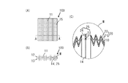
- FIG. 1 (A) shows the adhesion surface of the adsorbing member.
- FIG. 1B is a cross-sectional view taken along the line AA ′ in FIG.
- FIG. 1C is an enlarged cross-sectional view of the suction surface portion M.
- the adsorbing member 100 of the present invention is a member used to temporarily adsorb and hold the label L when adhering the label L to an adherend, and is used as an internal assembly in a label adhering device or a label adhering line.
- the adsorbing member 100 includes a base material 10 and a pad portion 20 that covers the base material surface.
- Examples of the substrate 10 include various metals and various resins.
- plate-like aluminum which is a light metal material excellent in shape stability and processability, is used.
- the substrate 10 has a plate shape composed of a substrate surface 12 and a substrate back surface 13 on which a plurality of linear recesses 11 are formed, and a large number of holes 14 penetrating the front and back are formed.
- the pad portion 20 includes a sintered body layer 21 that is formed by thermal spraying on the substrate surface 12 and a silicon-based resin layer 22 that is formed by coating the surface of the sintered body layer 21. *
- Examples of the coating material for the sintered body layer 21 include inorganic sintered bodies (ceramics), metal sintered bodies (sintering metals), and organic sintered bodies (sintered plastics). Use superior ceramics. Specifically, white alumina, gray alumina, alumina zirconia, alumina titania, chromium oxide, zirconia-yttria, etc. are preferably used.
- the base material 10 and the coating material are physically bonded by a thermal spray molding method.
- the thermal spray molding method is a technique in which a ceramic film, which is a melted (semi-molten) film material, is sprayed onto the substrate surface 12 by gas (air, carrier gas) to form a film.
- a dense sintered body layer 21 is formed on the substrate surface 12 by thermal spray molding. In the formed sintered body layer 21, a sintered hole 23 that is electrically connected to the hole 14 is formed. *
- the silicon-based resin used for the silicon-based resin layer 22 may be organic polysiloxane having general resin properties, and is preferably a blend of alkyd resin or acrylic resin in order to improve paintability.
- the sintered body layer 21 and the silicon-based resin are physically bonded by plasma coating.
- the plasma coating is a technique for forming a film by plasma ionizing a silicon-based resin as a coating material and striking it on the sintered body layer 21. Compared to a normal spray coat or the like, a film having excellent uniformity and physical strength can be formed.
- Preferred film properties are film thickness: 200 ⁇ m, surface roughness Ra 1 ⁇ m to Ra 3 ⁇ m: surface hardness: HRC45.
- Resin holes 24 communicating with the sintered holes 23 are formed in the formed silicon-based resin layer 22.
- the communicating sintered hole 23 and the resin hole 24 form a communicating hole 25.
- the holes 14 communicate with an intake or exhaust device (not shown) so as to perform an intake or exhaust action individually or collectively as a part or as a whole. *
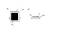
- FIG. 2A is an explanatory diagram of a state in which the label is adsorbed on the adsorption surface of the adsorption member 100.
- FIG. 1B is a cross-sectional view taken along line BB ′ in FIG.
- the adsorbing member 100 shown in FIG. 2B is provided with a first conduction hole 26 that conducts to the hole 14 communicated only with the intake device.
- the adsorbing member 100 adsorbs the label L to the pad portion 20 by the suction action by the first conduction hole 26.
- the adhesive of the label L has no fear of adhering to the suction surface because the suction surface is formed of a silicon-based resin having excellent non-stickiness.
- the suction surface has a shape reflecting the concave portion 11, the contact area with the label L is reduced, and the suction force required for label suction can be suppressed. *
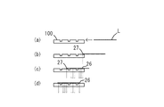
- the adsorbing member 100 shown in FIG. 3 includes a first conduction hole 26 communicated with the intake device and a second conduction hole 27 communicated with the exhaust device.
- the conduction hole 25 changes to the first conduction hole 26 or the second conduction hole 27 according to the suction operation.
- the change of the conduction hole 25 is performed by changing the device to communicate with. *
- FIG. 3A shows a process in which the peeled label L is conveyed to the adsorption member 100. At this time, the conduction hole 25 has no intake or exhaust action.
- FIG. 3B shows a state in which the label L starts to slidably contact the suction surface.
- the conduction hole 25 close to the end of the label L acts as the second conduction hole 27 so that the end of the label L does not contact the suction surface. Since the end portion of the label L where the adhesive may protrude is not in contact with the adhesive surface, the adhesive does not adhere to the adsorption surface.
- FIG. 3A shows a process in which the peeled label L is conveyed to the adsorption member 100. At this time, the conduction hole 25 has no intake or exhaust action.
- FIG. 3B shows a state in which the label L starts to slidably contact the suction surface.
- the conduction hole 25 close to the end of the label L acts as the second conduction hole 27 so that the end of the label L does
- FIG. 3C shows a state where the label L moves on the suction surface.
- the conduction hole 25 where the end of the label L is located acts as the second conduction hole 27, and the conduction hole 25 covered with the label L acts as the first conduction hole 26.
- the second conduction hole 27 also moves.
- FIG. 3D shows a state where the label L is positioned at the suction position. At this time, the conduction hole 25 covered with the label L acts as the first conduction hole 26.
- the said description assumed that the adhesive agent protruded only from the moving front-end
- the conduction hole 25 corresponding to a place where the adhesive may ooze out from the rear end or the side end of the label L can act as the second conduction hole 27.
- suction member of this invention forms the adsorption
- the suction surface has a shape reflecting the concave portion of the base material, the contact area with the label is reduced, and the suction force required for label suction and the separation force required for sticking can be suppressed.
- exhaust is performed to the conduction hole corresponding to the portion where the adhesive may ooze out, and the adhesive is prevented from coming into contact with the suction surface. That is, it is possible to consciously prevent the adhesive protruding from the label from adhering to the adsorption surface.
- Adsorbing member 10 Substrate 11 Recess 12 Substrate surface 13 Substrate surface 14 Substrate back surface 14 Hole 20 Pad part 21 Sintered body layer 22 Silicone resin layer 23 Sintered hole 24 Resin hole 25 Conductive hole 26 First conductive hole 27 Second conductive Hole L Label M Adsorption surface part
Landscapes
- Labeling Devices (AREA)
- Manipulator (AREA)
Abstract
L'invention comporte un substrat (10), dans lequel une pluralité de trous (14) ont été formés; et un élément plat (20), qui couvre la surface du substrat (10) et comporte un trou traversant (25) interconnectant les trous (14). Un élément d'aspiration (100), dans lequel l'élément plat (20) est formé à partir d'une couche de corps fritté (21) moulée par pulvérisation sur la surface (12) du substrat et d'une couche de résine (23) à base de silicium, formée comme un revêtement sur la surface de la couche du corps fritté, permet de maintenir l'opération de fixation par aspiration d'une étiquette pendant une longue durée, par rapport à des éléments d'aspiration classiques équipés d'un élément plat comprenant une résine fluorée.
Applications Claiming Priority (2)
| Application Number | Priority Date | Filing Date | Title |
|---|---|---|---|
| JP2011-095591 | 2011-04-22 | ||
| JP2011095591A JP5901138B2 (ja) | 2011-04-22 | 2011-04-22 | 吸着部材 |
Publications (1)
| Publication Number | Publication Date |
|---|---|
| WO2012144232A1 true WO2012144232A1 (fr) | 2012-10-26 |
Family
ID=47041361
Family Applications (1)
| Application Number | Title | Priority Date | Filing Date |
|---|---|---|---|
| PCT/JP2012/002748 Ceased WO2012144232A1 (fr) | 2011-04-22 | 2012-04-20 | Elément d'aspiration |
Country Status (2)
| Country | Link |
|---|---|
| JP (1) | JP5901138B2 (fr) |
| WO (1) | WO2012144232A1 (fr) |
Citations (3)
| Publication number | Priority date | Publication date | Assignee | Title |
|---|---|---|---|---|
| JPS63317439A (ja) * | 1988-05-27 | 1988-12-26 | Terumo Corp | 可撓性物品のラベル貼着用金型 |
| JP2008094468A (ja) * | 2006-10-16 | 2008-04-24 | Sato Corp | ラベル貼付装置 |
| JP2010222008A (ja) * | 2009-03-19 | 2010-10-07 | Lintec Corp | ラベル貼付装置 |
-
2011
- 2011-04-22 JP JP2011095591A patent/JP5901138B2/ja active Active
-
2012
- 2012-04-20 WO PCT/JP2012/002748 patent/WO2012144232A1/fr not_active Ceased
Patent Citations (3)
| Publication number | Priority date | Publication date | Assignee | Title |
|---|---|---|---|---|
| JPS63317439A (ja) * | 1988-05-27 | 1988-12-26 | Terumo Corp | 可撓性物品のラベル貼着用金型 |
| JP2008094468A (ja) * | 2006-10-16 | 2008-04-24 | Sato Corp | ラベル貼付装置 |
| JP2010222008A (ja) * | 2009-03-19 | 2010-10-07 | Lintec Corp | ラベル貼付装置 |
Also Published As
| Publication number | Publication date |
|---|---|
| JP5901138B2 (ja) | 2016-04-06 |
| JP2012224387A (ja) | 2012-11-15 |
Similar Documents
| Publication | Publication Date | Title |
|---|---|---|
| TW200636905A (en) | Suction device, polishing device, semiconductor device and manufacturing method of semiconductor device | |
| WO2006091519A3 (fr) | Systeme d'usinage rapide et procedes de fabrication d'articles abrasifs | |
| JP2005503947A5 (fr) | ||
| EP2058378A4 (fr) | Matériau de revêtement destiné à former une couche barrière contre les gaz et corps multicouche barrière contre les gaz | |
| ATE416914T1 (de) | Laminierter körper | |
| KR102488733B1 (ko) | 첩합 디바이스의 제조 장치 | |
| WO2008128948A3 (fr) | Composant présentant un corps céramique métallisé | |
| EP2374612A8 (fr) | Matériau pour film métallique de surface, son procédé de fabrication, procédé de fabrication d'un matériau de motif métallique et matériau de motif métallique | |
| KR20130142095A (ko) | 흡착 필름과 그 제조 방법, 및 이형 필름이 부착된 흡착 필름과 그 제조 방법 | |
| JP2005205888A5 (fr) | ||
| US11548194B2 (en) | Method for manufacturing fluid device composite member | |
| JP2010135443A (ja) | 真空吸着パッドおよび真空吸着装置 | |
| EP2133922A3 (fr) | Revêtement isolant, procédés de fabrication associés et articles le comportant | |
| JP2018041776A (ja) | チャックテーブル及び搬送パッド | |
| WO2007019014A3 (fr) | Textile architectural | |
| JP5901138B2 (ja) | 吸着部材 | |
| JP2013226769A (ja) | 白色反射膜付基材、それを用いた白色反射膜付カバーレイシート及び白色反射膜付回路基板 | |
| WO2008045022A3 (fr) | Particules d'additif présentant des caractéristiques superhydrophobes et revêtements et procédés de fabrication et d'utilisation de celles-ci | |
| JP3179929U (ja) | 機能性シート部材 | |
| CN109478525A (zh) | 基板载体 | |
| ATE543209T1 (de) | Halbleitende struktur auf einem substrat mit starker rauheit | |
| CN111433388B (zh) | 基板用保护具以及附膜基板的制造方法 | |
| WO2017180502A1 (fr) | Préparation de circuits électriques par transfert d'adhésif | |
| JP3179220U (ja) | 耐摩耗性シート部材 | |
| KR102365285B1 (ko) | 제품 기판을 코팅하기 위한 방법 및 장치 |
Legal Events
| Date | Code | Title | Description |
|---|---|---|---|
| 121 | Ep: the epo has been informed by wipo that ep was designated in this application |
Ref document number: 12774620 Country of ref document: EP Kind code of ref document: A1 |
|
| NENP | Non-entry into the national phase |
Ref country code: DE |
|
| 122 | Ep: pct application non-entry in european phase |
Ref document number: 12774620 Country of ref document: EP Kind code of ref document: A1 |