WO2012141122A1 - 半導体集積回路装置および半導体集積回路装置の製造方法 - Google Patents
半導体集積回路装置および半導体集積回路装置の製造方法 Download PDFInfo
- Publication number
- WO2012141122A1 WO2012141122A1 PCT/JP2012/059642 JP2012059642W WO2012141122A1 WO 2012141122 A1 WO2012141122 A1 WO 2012141122A1 JP 2012059642 W JP2012059642 W JP 2012059642W WO 2012141122 A1 WO2012141122 A1 WO 2012141122A1
- Authority
- WO
- WIPO (PCT)
- Prior art keywords
- channel
- region
- film
- integrated circuit
- semiconductor integrated
- Prior art date
- Legal status (The legal status is an assumption and is not a legal conclusion. Google has not performed a legal analysis and makes no representation as to the accuracy of the status listed.)
- Ceased
Links
Images











Classifications
-
- H—ELECTRICITY
- H10—SEMICONDUCTOR DEVICES; ELECTRIC SOLID-STATE DEVICES NOT OTHERWISE PROVIDED FOR
- H10D—INORGANIC ELECTRIC SEMICONDUCTOR DEVICES
- H10D84/00—Integrated devices formed in or on semiconductor substrates that comprise only semiconducting layers, e.g. on Si wafers or on GaAs-on-Si wafers
- H10D84/80—Integrated devices formed in or on semiconductor substrates that comprise only semiconducting layers, e.g. on Si wafers or on GaAs-on-Si wafers characterised by the integration of at least one component covered by groups H10D12/00 or H10D30/00, e.g. integration of IGFETs
- H10D84/82—Integrated devices formed in or on semiconductor substrates that comprise only semiconducting layers, e.g. on Si wafers or on GaAs-on-Si wafers characterised by the integration of at least one component covered by groups H10D12/00 or H10D30/00, e.g. integration of IGFETs of only field-effect components
- H10D84/83—Integrated devices formed in or on semiconductor substrates that comprise only semiconducting layers, e.g. on Si wafers or on GaAs-on-Si wafers characterised by the integration of at least one component covered by groups H10D12/00 or H10D30/00, e.g. integration of IGFETs of only field-effect components of only insulated-gate FETs [IGFET]
-
- H—ELECTRICITY
- H10—SEMICONDUCTOR DEVICES; ELECTRIC SOLID-STATE DEVICES NOT OTHERWISE PROVIDED FOR
- H10D—INORGANIC ELECTRIC SEMICONDUCTOR DEVICES
- H10D30/00—Field-effect transistors [FET]
- H10D30/01—Manufacture or treatment
- H10D30/021—Manufacture or treatment of FETs having insulated gates [IGFET]
-
- H—ELECTRICITY
- H10—SEMICONDUCTOR DEVICES; ELECTRIC SOLID-STATE DEVICES NOT OTHERWISE PROVIDED FOR
- H10D—INORGANIC ELECTRIC SEMICONDUCTOR DEVICES
- H10D84/00—Integrated devices formed in or on semiconductor substrates that comprise only semiconducting layers, e.g. on Si wafers or on GaAs-on-Si wafers
- H10D84/01—Manufacture or treatment
- H10D84/0123—Integrating together multiple components covered by H10D12/00 or H10D30/00, e.g. integrating multiple IGBTs
- H10D84/0126—Integrating together multiple components covered by H10D12/00 or H10D30/00, e.g. integrating multiple IGBTs the components including insulated gates, e.g. IGFETs
- H10D84/0165—Integrating together multiple components covered by H10D12/00 or H10D30/00, e.g. integrating multiple IGBTs the components including insulated gates, e.g. IGFETs the components including complementary IGFETs, e.g. CMOS devices
- H10D84/0172—Manufacturing their gate conductors
- H10D84/0177—Manufacturing their gate conductors the gate conductors having different materials or different implants
-
- H—ELECTRICITY
- H10—SEMICONDUCTOR DEVICES; ELECTRIC SOLID-STATE DEVICES NOT OTHERWISE PROVIDED FOR
- H10D—INORGANIC ELECTRIC SEMICONDUCTOR DEVICES
- H10D84/00—Integrated devices formed in or on semiconductor substrates that comprise only semiconducting layers, e.g. on Si wafers or on GaAs-on-Si wafers
- H10D84/01—Manufacture or treatment
- H10D84/0123—Integrating together multiple components covered by H10D12/00 or H10D30/00, e.g. integrating multiple IGBTs
- H10D84/0126—Integrating together multiple components covered by H10D12/00 or H10D30/00, e.g. integrating multiple IGBTs the components including insulated gates, e.g. IGFETs
- H10D84/0165—Integrating together multiple components covered by H10D12/00 or H10D30/00, e.g. integrating multiple IGBTs the components including insulated gates, e.g. IGFETs the components including complementary IGFETs, e.g. CMOS devices
- H10D84/0188—Manufacturing their isolation regions
-
- H—ELECTRICITY
- H10—SEMICONDUCTOR DEVICES; ELECTRIC SOLID-STATE DEVICES NOT OTHERWISE PROVIDED FOR
- H10D—INORGANIC ELECTRIC SEMICONDUCTOR DEVICES
- H10D84/00—Integrated devices formed in or on semiconductor substrates that comprise only semiconducting layers, e.g. on Si wafers or on GaAs-on-Si wafers
- H10D84/01—Manufacture or treatment
- H10D84/02—Manufacture or treatment characterised by using material-based technologies
- H10D84/03—Manufacture or treatment characterised by using material-based technologies using Group IV technology, e.g. silicon technology or silicon-carbide [SiC] technology
- H10D84/038—Manufacture or treatment characterised by using material-based technologies using Group IV technology, e.g. silicon technology or silicon-carbide [SiC] technology using silicon technology, e.g. SiGe
-
- H—ELECTRICITY
- H10—SEMICONDUCTOR DEVICES; ELECTRIC SOLID-STATE DEVICES NOT OTHERWISE PROVIDED FOR
- H10D—INORGANIC ELECTRIC SEMICONDUCTOR DEVICES
- H10D84/00—Integrated devices formed in or on semiconductor substrates that comprise only semiconducting layers, e.g. on Si wafers or on GaAs-on-Si wafers
- H10D84/80—Integrated devices formed in or on semiconductor substrates that comprise only semiconducting layers, e.g. on Si wafers or on GaAs-on-Si wafers characterised by the integration of at least one component covered by groups H10D12/00 or H10D30/00, e.g. integration of IGFETs
- H10D84/82—Integrated devices formed in or on semiconductor substrates that comprise only semiconducting layers, e.g. on Si wafers or on GaAs-on-Si wafers characterised by the integration of at least one component covered by groups H10D12/00 or H10D30/00, e.g. integration of IGFETs of only field-effect components
- H10D84/83—Integrated devices formed in or on semiconductor substrates that comprise only semiconducting layers, e.g. on Si wafers or on GaAs-on-Si wafers characterised by the integration of at least one component covered by groups H10D12/00 or H10D30/00, e.g. integration of IGFETs of only field-effect components of only insulated-gate FETs [IGFET]
- H10D84/8314—Integrated devices formed in or on semiconductor substrates that comprise only semiconducting layers, e.g. on Si wafers or on GaAs-on-Si wafers characterised by the integration of at least one component covered by groups H10D12/00 or H10D30/00, e.g. integration of IGFETs of only field-effect components of only insulated-gate FETs [IGFET] the IGFETs characterised by having gate insulating layers with different properties
Definitions
- the present invention relates to a technology effective when applied to a semiconductor integrated circuit device and a threshold voltage control technology in a method of manufacturing a semiconductor integrated circuit device (or a semiconductor device).
- Non-Patent Document 1 includes an n-MISFET (Metal Insulator Semiconductor Field Effect Transistor) having a High-k gate insulating film and a p-MISFET.
- n-MISFET Metal Insulator Semiconductor Field Effect Transistor
- another kind of metal or metal oxide is formed on the High-k gate insulating film in each region, and the components are reduced.
- Non-Patent Document 2 In order to control the threshold voltage of the n-MISFET and the p-MISFET, the concentration of the additive component introduced into the High-k gate insulating film is not lowered due to diffusion caused by subsequent high-temperature heat treatment or the like.
- -K gate insulating film Technique of extending the Engineering end to offset side wall end portion is disclosed.
- High-k gate insulating films and metal gate electrodes are introduced in MISFETs used for SOC (System on Chip) and the like after the 32 nm technology node.
- MISFETs System on Chip
- the absolute value of the threshold voltage of the n-MISFET and the p-MISFET is increased by the subsequent high-temperature heat treatment. Therefore, by forming various threshold voltage adjusting metal films or threshold voltage adjusting metal oxide films on the High-k gate insulating film, and introducing these film components into the High-k gate insulating film therefrom. The threshold voltage is controlled.
- An object of the present invention is to provide a highly reliable semiconductor integrated circuit device or a manufacturing process of a semiconductor integrated circuit device.
- the N-channel threshold adjustment element outward diffusion prevention region is provided in the lower part of the gate stack of the n-MISFET and on the surface of the element isolation region around it, the high-k gate insulation of the n-MISFET Lanthanum or the like introduced into the film can be prevented from moving to an STI region (element isolation region) or the like by a subsequent heat treatment.
- FIG. 2 is a device cross-sectional view corresponding to the X-X ′ cross section of FIG. 1.
- FIG. 2 is a device sectional view corresponding to a Y-Y ′ section in FIG. 1; 1 is a device cross-sectional view (STI) corresponding to the XX ′ cross-section of FIG. 1 for explaining a main process in the method for manufacturing a semiconductor integrated circuit device according to the embodiment of the present application (N-channel threshold adjusting element ion implantation method). The region is being formed).
- STI device cross-sectional view
- 1 is a device cross-sectional view corresponding to the XX ′ cross section of FIG. 1 for explaining a main process in the method for manufacturing a semiconductor integrated circuit device according to the embodiment of the present application (N-channel threshold adjusting element ion implantation method). Channel threshold adjustment element ion implantation step).
- 1 is a device cross-sectional view (STI) corresponding to the XX ′ cross-section of FIG. 1 for explaining a main process in the method for manufacturing a semiconductor integrated circuit device according to the embodiment of the present application (N-channel threshold adjusting element ion implantation method).
- 1 is a device cross-sectional view (well) corresponding to the XX ′ cross section of FIG.
- 1 for explaining a main process in the method for manufacturing a semiconductor integrated circuit device according to the embodiment of the present application (N-channel threshold adjustment element ion implantation method); Region forming step).
- 1 is a device cross-sectional view corresponding to the XX ′ cross section of FIG. 1 for explaining a main process in the method for manufacturing a semiconductor integrated circuit device according to the embodiment of the present application (N-channel threshold adjustment element ion implantation method). This is a resist film forming step for hard mask for channel threshold adjustment film processing).
- 1 is a device cross-sectional view corresponding to the XX ′ cross section of FIG. 1 for explaining a main process in the method for manufacturing a semiconductor integrated circuit device according to the embodiment of the present application (N-channel threshold adjustment element ion implantation method).
- 1 for explaining a main process in the method for manufacturing a semiconductor integrated circuit device according to the embodiment of the present application (N-channel threshold adjusting element ion implantation method).
- 1 is a device cross-sectional view corresponding to the XX ′ cross section of FIG. 1 for explaining a main process in the method for manufacturing a semiconductor integrated circuit device according to the embodiment of the present application (N-channel threshold adjustment element ion implantation method).
- 1 is a device cross-sectional view (metal) corresponding to the XX ′ cross-section of FIG. 1 for explaining a main process in the method for manufacturing a semiconductor integrated circuit device according to the embodiment of the present application (N-channel threshold adjustment element ion implantation method).
- 1 for explaining a main process in the method for manufacturing a semiconductor integrated circuit device according to the embodiment of the present application (N-channel threshold adjusting element ion implantation method).
- Channel threshold adjustment element-containing film patterning step). 1 is a device cross-sectional view corresponding to the XX ′ cross section of FIG. 1 for explaining a main process in the method for manufacturing a semiconductor integrated circuit device according to the embodiment of the present application (N-channel threshold adjusting element ion implantation method).
- Channel threshold adjustment element-containing film patterning heat treatment step). 1 is a device cross-sectional view corresponding to the XX ′ cross section of FIG.
- 1 for explaining a main process in the method for manufacturing a semiconductor integrated circuit device according to the embodiment of the present application (N-channel threshold adjusting element ion implantation method).
- 1 is a device cross-sectional view corresponding to the XX ′ cross section of FIG. 1 for explaining a main process in the method for manufacturing a semiconductor integrated circuit device according to the embodiment of the present application (N-channel threshold adjusting element ion implantation method).
- Channel threshold value adjusting element-containing film sidewall forming step). 1 is a device cross-sectional view corresponding to the XX ′ cross section of FIG.
- N-channel threshold adjusting element ion implantation method N-channel threshold adjusting element ion implantation method.
- Channel threshold adjustment element-containing film sidewall removal step 1 is a device cross-sectional view (STI) corresponding to the XX ′ cross-section of FIG. 1 for explaining a main process in the method for manufacturing a semiconductor integrated circuit device according to the embodiment of the present application (N-channel threshold adjusting element ion implantation method).
- Forming silicon nitride film removal step). 1 corresponds to the XX ′ cross section of FIG. 1 for explaining Modification 3 (N channel threshold value adjusting element-containing film formation & hard mask method) of the method for manufacturing a semiconductor integrated circuit device of one embodiment of the present application.
- FIG. 1 corresponds to the XX ′ cross section of FIG. 1 for explaining Modification 3 (N channel threshold value adjusting element-containing film formation & hard mask method) of the method for manufacturing a semiconductor integrated circuit device of one embodiment of the present application.
- It is device sectional drawing (N channel threshold value adjustment element containing film
- FIG. 28 is a device sectional view corresponding to a section taken along line X-X ′ of FIG. 27.
- FIG. 28 is a device sectional view corresponding to a Y-Y ′ section in FIG.
- Semiconductor integrated circuit devices including: (A) an element isolation region provided on the surface of the first main surface of the semiconductor substrate; (B) an N channel active region and a P channel active region provided on the surface of the first main surface of the semiconductor substrate and separated from each other by the element isolation region; (C) an N-channel gate stack which is provided on the first main surface of the semiconductor substrate and traverses the N-channel active region and constitutes an N-channel MISFET; (D) a P-channel gate stack which is provided on the first main surface of the semiconductor substrate and traverses the P-channel active region and constitutes a P-channel MISFET; (E) An N channel threshold adjustment element outward diffusion prevention region provided in a surface region of the element isolation region under and around the N channel gate stack.
- the N channel threshold adjustment element outward diffusion prevention region is doped with an N channel threshold adjustment element.
- the N channel threshold adjustment element outward diffusion prevention region is doped with nitrogen.
- the N channel threshold adjustment element outward diffusion prevention region is formed by ion implantation of the N channel threshold adjustment element.
- the N channel threshold value adjusting element outward diffusion preventing region is formed by ion implantation of nitrogen.
- N channel threshold adjustment element outward diffusion prevention region is formed by forming a surface of the element isolation region in a portion to be the N channel threshold adjustment element outward diffusion prevention region.
- an N channel threshold adjusting element or an oxide thereof is formed and heat-treated.
- the N channel threshold value adjusting element is La, Y, Mg, or Sc.
- semiconductor device or “semiconductor integrated circuit device” mainly refers to various types of transistors (active elements) alone, and resistors, capacitors, etc. as semiconductor chips (eg, single crystal). The one integrated on the silicon substrate).
- MISFET Metal Insulator Semiconductor Effect Transistor
- MOSFET Metal Oxide Field Element Effect Transistor
- CMOS Complementary Metal Oxide Semiconductor
- a semiconductor process of today's semiconductor integrated circuit device is usually carried out from the introduction of a silicon wafer as a raw material to a premetal process (interlayer insulating film between the lower end of the M1 wiring layer and the gate electrode structure).
- a premetal process interlayer insulating film between the lower end of the M1 wiring layer and the gate electrode structure.
- FEOL Front End of Line
- M1 wiring layer formation to the process of forming a contact hole, tungsten plug, embedding, etc.
- the pad opening to the final passivation film on the aluminum-based pad electrode Can be roughly divided into BEOL (Back End of Line) processes up to the formation of the wafer (including the process in the wafer level package process).
- the gate electrode patterning process, the contact hole forming process, and the like are microfabrication processes that require particularly fine processing.
- a via and trench formation process in particular, a relatively lower local wiring (for example, M1 to M3 in a buried wiring having a structure of about four layers, M1 in a buried wiring having a structure of about 10 layers.
- fine processing is required for fine embedded wiring from M to around M5.
- M1 is a first layer wiring
- M3 is a third layer wiring.
- the material, composition, etc. may be referred to as “X consisting of A”, etc., except when clearly stated otherwise and clearly from the context, except for A It does not exclude what makes an element one of the main components.
- the component it means “X containing A as a main component”.
- silicon member is not limited to pure silicon, but also includes SiGe alloys, other multi-component alloys containing silicon as a main component, and members containing other additives. Needless to say.
- silicon oxide film not only relatively pure undoped silicon oxide (Undoped Silicon Dioxide), but also FSG (Fluorosilicate Glass), TEOS-based silicon oxide ( Thermal oxide films such as TEOS-based silicon oxide, SiOC (Silicon Oxicarbide), carbon-doped silicon oxide, or OSG (Organosilicate glass), PSG (Phosphorus Silicate glass), BPSG (Borophosphosilicate glass), CVD Oxide film, SOG (Spin ON Glass), nano-clustering silica (Nano-Clustering Silica: NCS) coated silicon oxide, silica-based low-k insulating film (porous insulating) Needless to say, a film) and a composite film with other silicon-based insulating films including these as main constituent elements are included.
- FSG Fluorosilicate Glass
- TEOS-based silicon oxide Thermal oxide films such as TEOS-based silicon oxide, SiOC (Silicon Oxicarbide), carbon-d
- silicon nitride insulating films that are commonly used in the semiconductor field include silicon nitride insulating films.
- Materials belonging to this system include SiN, SiCN, SiNH, SiCNH, and the like.
- SiN silicon nitride
- SiNH silicon nitride
- SiCNH silicon nitride insulating films.
- SiC has similar properties to SiN, but SiON is often classified as a silicon oxide insulating film.
- the silicon nitride film is frequently used as an etch stop film or CESL (Contact Etch Stop Layer) in SAC (Self-Aligned Contact) technology, and also as a stress applying film (stressor or stressor film) in SMT (Stress Memoryization Technique). used.
- nickel silicide usually refers to nickel monosilicide, but includes not only relatively pure ones but also alloys, mixed crystals, and the like whose main components are nickel monosilicide. Further, the silicide is not limited to nickel silicide, but may be cobalt silicide, titanium silicide, tungsten silicide, or the like that has been proven in the past.
- the metal film for silicidation includes, for example, a Ni—Pt alloy film (Ni and Pt alloy film), a Ni—V alloy film (Ni and V alloy film), A nickel alloy film such as a Ni—Pd alloy film (Ni and Pd alloy film), a Ni—Yb alloy film (Ni and Yb alloy film) or a Ni—Er alloy film (Ni and Er alloy film) is used. be able to.
- nickel-based silicide silicides having nickel as a main metal element are collectively referred to as “nickel-based silicide”.
- “Wafer” usually refers to a single crystal silicon wafer on which a semiconductor integrated circuit device (same as a semiconductor device and an electronic device) is formed, but an insulating substrate such as an epitaxial wafer, an SOI substrate, an LCD glass substrate and the like. Needless to say, a composite wafer such as a semiconductor layer is also included.
- gate includes “real gate”, that is, what is actually a gate, and so-called “dummy gate” and “replacement gate” that are removed later.
- the “gate stack” refers to a stacked body mainly composed of a gate insulating film and a gate electrode (referred to as an “actual gate stack” when it is particularly necessary to distinguish from a “dummy gate stack”).
- the term “High-k gate stack” refers to a gate insulating film having a High-k gate insulating layer.
- gate side structure refers to gate peripheral structures such as offset spacers and sidewall spacers formed on the side walls of the gate stack. Further, the gate peripheral structure including the gate stack and the gate side surface structure is referred to as a “gate structure”.
- the “gate first method” refers to a method in which the formation of the actual gate stack is performed before the activation heat treatment of the source / drain in the manufacturing method of the integrated circuit device in which the MISFET is integrated.
- the “gate last method” refers to a method in which the main elements of the actual gate stack are formed after the activation heat treatment of the source and drain.
- the interface gate insulating film (interface actual gate insulating film) and the high-k gate insulating film (actual gate insulating film) are executed before the activation heat treatment of the source / drain
- a method of forming the main elements of the gate stack after the activation heat treatment of the source / drain is called “High-k first-metal gate last method”.
- the interface gate insulating film (so-called IL) and the high-k gate insulating film are elements constituting the dummy gate stack, but are also elements constituting the actual gate stack. Therefore, the name at that time may be used in the description of the process.
- an “active region” is a region surrounded by an element isolation region on the device surface of a semiconductor substrate, and refers to a portion to be a channel region or a source / drain region of a MISFET or the like.
- hatching or the like may be omitted even in a cross section when it becomes complicated or when it is clearly distinguished from a gap.
- the contour line of the background may be omitted even if the hole is planarly closed.
- it may be hatched to clearly indicate that it is not a void.
- the gate first method will be mainly described for convenience of explanation, but it goes without saying that the present invention can also be applied to a gate last method including an intermediate form such as a High-k first-metal gate last method.
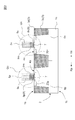
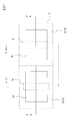
- FIG. 1 is a top view of an essential part of a device for explaining a device structure (N-channel threshold adjustment element-doped STI structure) and the like of a semiconductor integrated circuit device according to an embodiment of the present application.
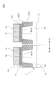
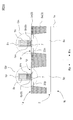
- FIG. 2 is a device cross-sectional view corresponding to the X-X ′ cross section of FIG. 1.
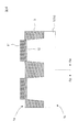
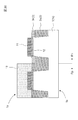
- FIG. 3 is a device cross-sectional view corresponding to the Y-Y ′ cross section of FIG. 1. Based on these, the device structure (N-channel threshold adjustment element doped STI structure) of the semiconductor integrated circuit device according to the embodiment of the present application will be described.
- the semiconductor chip 2 is divided into a substrate portion 1s (P-type single crystal silicon substrate portion) and a well portion thereon, and the well portion corresponds to the N channel device region Rn. It is divided into an N-type well region 6n and a P-type well region 6p corresponding to the P-channel device region Rp.
- An N-type source / drain region 20n and a P-type source / drain region 20p are provided in the surface regions of the N-channel gate stack 5n and the P-channel gate stack 5p, respectively.
- the N-channel gate stack 5n includes, from below, an IL (Interfacial Layer), that is, an interfacial silicon oxide insulating film 7, an N-channel High-k gate insulating film 8n (High-k gate insulating film 8), a metal gate electrode film 9m, a poly It is composed of a silicon gate electrode film 9s and the like.
- the P channel gate stack 5p is composed of an IL, that is, an interfacial silicon oxide insulating film 7, a P channel High-k gate insulating film 8p (High-k gate insulating film 8), a metal gate electrode film 9m, a polysilicon gate from the bottom.
- the electrode film is composed of 9s and the like.
- an N channel threshold adjustment element introduction region 3d is provided on the surface of the STI region 3 (element isolation region) below or around the N channel gate stack 5n.
- the N channel threshold adjustment element introduction region 3d is not provided on the surface of the STI region 3 (element isolation region) below or around the P channel gate stack 5p. This is because the threshold voltage control of the P channel MISFET (Qp) is adversely affected.
- the N-channel threshold adjustment element introduction region 3d is generally almost the entire surface region of the STI region 3 (element isolation region) corresponding to the N-channel device region Rn for ease of manufacturing. However, it may be formed only on the surface region of the STI region 3 (element isolation region) below or around the N-channel gate stack 5n.
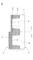
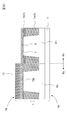
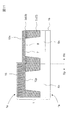
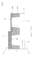
- FIG. 1 for explaining the main process in the method of manufacturing a semiconductor integrated circuit device (N channel threshold value adjusting element ion implantation method) of the one embodiment of the present application. It is a figure (STI formation silicon nitride film etc. removal process). 7 is a device cross-section corresponding to the XX ′ cross-section of FIG. 1 for explaining the main process in the method of manufacturing a semiconductor integrated circuit device according to the embodiment of the present application (N-channel threshold adjustment element ion implantation method). It is a figure (well area
- FIG. 8 is a device cross-section corresponding to the XX ′ cross-section of FIG.
- FIG. 11 is a device cross-section corresponding to the XX ′ cross-section of FIG. 1 for explaining the main process in the method for manufacturing a semiconductor integrated circuit device (N-channel threshold adjustment element ion implantation method) of the one embodiment of the present application. It is a figure (N channel threshold value adjustment film
- the silicon nitride film 11 for STI formation and the pad silicon oxide film 12 are patterned by normal lithography (for example, ArF lithography) to form a trench formation opening (for example, a width of about 70 nm).
- a trench for example, a depth of about 300 nm is formed by anisotropic dry etching using a halogen-based etching gas, for example, using the patterned silicon nitride film 11 for forming STI as a mask.
- a liner silicon oxide film (for example, about 3 nm thick) is formed in the trench by, for example, thermal oxidation.
- a buried silicon oxide film is formed on almost the entire device surface 1a side of the wafer 1 and in the trench by, for example, HDP (High Density Plasma) -CVD.
- the surface is planarized by, for example, CMP (Chemical Mechanical Polishing), and stopped on the STI forming silicon nitride film 11.
- CMP Chemical Mechanical Polishing
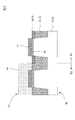
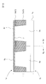
- the N-channel threshold adjustment element introduction resist film 14 (for example, about 300 nm thick) is patterned by normal lithography (for example, ArF lithography). For example, lanthanum is ion-implanted into the surface of the STI region 3 corresponding to the N-channel device region Rn by using the patterned resist film 14 for introducing the N-channel threshold adjustment element as an ion implantation mask. Region 3d (N-channel threshold adjustment element outward diffusion prevention region) is formed.
- ion implantation conditions for example, ion species: lanthanum, implantation energy: about 150 KeV, dose amount: 5 ⁇ 10 14 / cm 2 or the like (for example, implantation energy: about 50 to 300 KeV, dose amount: 5 ⁇ 10 13 / Cm 2 to 5 ⁇ 10 15 / cm 2 etc.) can be exemplified as a suitable one.
- ion implantation of lanthanum or the like is performed in the state where the silicon nitride film 11 for forming the STI and the pad silicon oxide film 12 are present, it is possible to prevent undesired introduction of lanthanum or the like into the N channel active region 4n. There is a merit that can be.
- the resist film 14 for introducing the N-channel threshold adjustment element that has become unnecessary is removed by, for example, ashing.
- the silicon nitride film 11 for forming the STI is removed by, for example, hot phosphoric acid, and the device surface 1a of the wafer 1 is etched back by using, for example, a hydrofluoric acid-based etchant, whereby the pad silicon oxide film 12 is obtained. When these are removed, the result is as shown in FIG.
- N-type well region 6n and P-type well region 6p are formed in the corresponding portions, respectively.
- a silicon oxide insulating film 7 (for example, a thickness) is formed on almost the entire semiconductor surface of the device surface 1a of the wafer 1 as an IL (interfacial oxide insulating film) by, for example, thermal oxidation.
- a silicon oxynitride film of about 1 nm is formed.
- a non-doped High-k gate insulating film 8 (for example, a hafnium oxide High-k gate insulating film having a thickness of about 2 nm) is formed on almost the entire surface of the interfacial silicon oxide insulating film 7 by, for example, ALD (Atomic Layer deposition). ).
- a P-channel threshold adjustment film 10p (for example, an alumina film having a thickness of about 1 nm) is formed on almost the entire surface of the non-doped High-k gate insulating film 8 by sputtering, for example.
- a metal cap film or a hard mask film 15 for processing the P channel threshold adjustment film (for example, a TiN film having a thickness of about 10 nm) is formed on almost the entire surface of the P channel threshold adjustment film 10p by, for example, reactive sputtering. Form a film.
- a P-channel threshold adjustment film processing hard mask resist film 16 (for example, a thickness of about 300 nm) is formed on the P-channel threshold adjustment film processing hard mask film 15, and this is applied to normal lithography (for example, ArF Patterning is performed by lithography.
- the P channel threshold adjustment film processing hard mask film 15 is patterned by, for example, wet etching using the P channel threshold adjustment film processing hard mask resist film 16 as a mask. Thereafter, the P-channel threshold adjustment film processing hard mask resist film 16 that has become unnecessary is removed.
- the P-channel threshold adjustment film 10p on the N-channel device region Rn side is removed, for example, by wet etching or the like.
- wet etching solution for example, SPM (Sulfuric Acid Peroxide Mixture) can be exemplified as a suitable one.
- an N-channel threshold adjustment film 10n (for example, a lanthanum oxide film having a thickness of about 1 nm) is formed on almost the entire surface of the wafer 1 on the device surface 1a side by, for example, sputtering film formation. To do. Thereafter, by performing a heat treatment (for example, an RTA process of about 850 degrees Celsius), as shown in FIG. 12, the non-doped High-k gate insulating film 8 in the N-channel device region Rn becomes an N-channel High-k gate insulating film. A film 8n (lanthanum-added hafnium oxide-based High-k gate insulating film) is formed.
- a heat treatment for example, an RTA process of about 850 degrees Celsius
- the non-doped High-k gate insulating film 8 in the P-channel device region Rp becomes a P-channel High-k gate insulating film 8p (aluminum-added hafnium oxide-based High-k gate insulating film).
- the P-channel threshold adjustment film processing hard mask film 15 that is no longer needed is removed by, for example, wet etching or the like, the result is as shown in FIG.
- a wet etching liquid SPM etc. can be illustrated as a suitable thing, for example.
- a metal gate electrode film 9m for example, a TiN film having a thickness of about 10 nm
- a polysilicon gate electrode film 9s (for example, a polysilicon film or an amorphous silicon film having a thickness of about 10 nm) is formed on almost the entire surface of the metal gate electrode film 9m by, for example, CVD.
- the N-channel gate stack 5n and the P-channel gate stack 5p are patterned by a combination of normal lithography (for example, ArF lithography) and anisotropic dry etching, for example.
- a halogen-based etching gas such as HBr
- a halogen-based etching gas such as Cl 2 / HBr
- an etching gas for the ⁇ k gate insulating film 8 (8n, 8p) for example, a halogen-based etching gas such as BCl 3 / Cl 2 can be exemplified as a preferable one.
- the process shifts to a copper-based buried wiring process such as a damascene method.
- FIG. 16 is a device cross-section corresponding to the XX ′ cross-section of FIG. 1 for explaining the main process in the method of manufacturing a semiconductor integrated circuit device according to the embodiment of the present application (N-channel threshold adjustment element ion implantation method). It is a figure (N channel threshold value adjustment element containing film
- FIG. 17 is a device cross section corresponding to the XX ′ cross section of FIG. 1 for explaining the main process in the method of manufacturing a semiconductor integrated circuit device according to the embodiment of the present application (N-channel threshold adjustment element ion implantation method). It is a figure (N channel threshold value adjustment element containing film
- 18 is a device cross-section corresponding to the XX ′ cross-section of FIG.
- FIG. 19 is a device cross-section corresponding to the XX ′ cross-section of FIG. 1 for explaining the main process in the method of manufacturing a semiconductor integrated circuit device according to the embodiment of the present application (N-channel threshold adjustment element ion implantation method). It is a figure (N channel threshold value adjustment element containing film
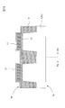
- an N channel threshold adjustment element-containing film 17 (for example, a lanthanum oxide film having a thickness of about 1 nm is formed on the entire surface of the wafer 1 on the device surface 1 a side by, for example, sputtering film formation. ).
- the resist film 17 for N-channel threshold adjustment element-containing film processing (for example, about 300 nm thick) is patterned by, for example, normal lithography (for example, ArF lithography).
- normal lithography for example, ArF lithography
- the N channel threshold adjustment element containing film 17 on the P channel device region Rp is removed, for example, by wet etching or the like.
- SPM etc. can be illustrated as a suitable thing, for example.
- the N-channel threshold adjustment element-containing film processing resist film 17 that is no longer needed is removed by, for example, ashing, as shown in FIG.
- N channel threshold adjustment element ion implantation method As described above, in the method of introducing the N channel threshold adjustment element from the N channel threshold adjustment element containing film (N channel threshold adjustment element containing film deposition basic method), a method by ion implantation (N channel threshold adjustment element ion implantation method). As compared with the above, there is an advantage that the high concentration N-channel threshold adjustment element-containing region 3d can be formed relatively easily.
- FIG. 20 is a device cross section corresponding to the XX ′ cross section of FIG. 1 for describing the main process in the method for manufacturing a semiconductor integrated circuit device (N-channel threshold adjustment element ion implantation method) of the one embodiment of the present application. It is a figure (N channel threshold value adjustment element containing film
- FIG. 21 is a device cross section corresponding to the XX ′ cross section of FIG. 1 for explaining the main process in the method of manufacturing a semiconductor integrated circuit device according to the embodiment of the present application (N channel threshold adjustment element ion implantation method). It is a figure (N channel threshold value adjustment element containing film
- FIG. 22 is a device cross section corresponding to the XX ′ cross section of FIG.
- N-channel threshold adjustment element ion implantation method N-channel threshold adjustment element ion implantation method. It is a figure (STI formation silicon nitride film etc. removal process). Based on these, a second modification of the method for manufacturing a semiconductor integrated circuit device according to the embodiment of the present application (N-channel threshold adjustment element-containing film formation & sidewall method) will be described.
- an N channel threshold adjustment element introduction region 3d (N A channel threshold adjustment element outward diffusion prevention region) is formed, and the element isolation region 3 is divided into this region and the original N-channel threshold adjustment element non-introduction region 3u as before.
- FIG. 23 is a cross-sectional view taken along the line XX ′ of FIG. 1 for explaining a third modification of the method for manufacturing a semiconductor integrated circuit device according to the embodiment of the present application (film formation with N-channel threshold value adjusting element-containing film and hard mask method).
- FIG. 6 is a device cross-sectional view corresponding to (P channel device region covering hard mask film forming step).
- 24 is a cross-sectional view taken along the line XX ′ of FIG. 1 for explaining a third modification of the method for manufacturing a semiconductor integrated circuit device according to the embodiment of the present application (N channel threshold value adjusting element-containing film formation & hard mask method).
- FIG. 4 is a device cross-sectional view corresponding to (P channel device region covering hard mask film patterning step).
- FIG. 25 is a cross-sectional view taken along the line XX ′ of FIG. 1 for explaining a third modification of the method for manufacturing a semiconductor integrated circuit device according to the embodiment of the present application (N-channel threshold adjustment element-containing film formation & hard mask method).
- FIG. 6 is a device cross-sectional view corresponding to (N channel threshold value adjusting element-containing film forming step).
- FIG. 26 is a cross-sectional view taken along the line XX ′ of FIG. 1 for explaining a third modification of the method for manufacturing a semiconductor integrated circuit device according to the embodiment of the present application (deposition of an N-channel threshold adjustment element-containing film and hard mask method).
- the cap film or the hard mask film 25 for covering the P channel device region (for example, by reactive sputtering film formation, for example, over almost the entire surface on the device surface 1 a side of the wafer 1.
- a TiN film having a thickness of about 10 nm is formed.
- TaN can be exemplified as a suitable material in addition to the TiN film.
- the resist film 26 for example, having a thickness of about 300 nm
- the resist film 26 for example, having a thickness of about 300 nm
- normal lithography for example, ArF lithography
- the P channel device region covering hard mask film 25 in the N channel device region Rn is removed by, for example, wet etching or the like.
- a wet etching liquid SPM etc. can be illustrated as a suitable thing, for example.
- the P-channel device region-covering hard mask processing resist film 26 that has become unnecessary is removed by, for example, ashing.
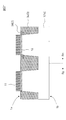
- an N-channel threshold adjustment element-containing film 17 (for example, a lanthanum oxide film having a thickness of about 1 nm) is formed on almost the entire surface of the wafer 1 on the device surface 1a side by, for example, sputtering film formation. Film.
- an N channel threshold value adjusting element introduction region 3d (N A channel threshold adjustment element outward diffusion prevention region) is formed, and the element isolation region 3 is divided into this region and the original N-channel threshold adjustment element non-introduction region 3u as before.
- the N-channel threshold adjustment element-containing film 17 and the P-channel device region covering hard mask film 25 are removed by wet etching using SPM, for example. Thereafter, the process proceeds to the process of FIG.
- the pattern accuracy can be improved as compared with patterning the N-channel threshold adjustment element-containing film 17 directly with a resist film.
- FIG. 27 is a top view of a device main part (corresponding to FIG. 1) for explaining a modified example (nitrogen-doped STI structure) of the device structure of the semiconductor integrated circuit device according to the embodiment of the present application.
- FIG. 28 is a device cross-sectional view corresponding to the X-X ′ cross section of FIG. 27.
- FIG. 29 is a device cross-sectional view corresponding to the Y-Y ′ cross section of FIG. 27.
- the semiconductor chip 2 is divided into a substrate portion 1s (P-type single crystal silicon substrate portion) and a well portion thereon, and the well portion corresponds to the N channel device region Rn. It is divided into an N-type well region 6n and a P-type well region 6p corresponding to the P-channel device region Rp.
- An N-type source / drain region 20n and a P-type source / drain region 20p are provided in the surface regions of the N-channel gate stack 5n and the P-channel gate stack 5p, respectively.
- the N-channel gate stack 5n includes, from below, an IL (Interfacial Layer), that is, an interfacial silicon oxide insulating film 7, an N-channel High-k gate insulating film 8n (High-k gate insulating film 8), a metal gate electrode film 9m, a poly It is composed of a silicon gate electrode film 9s and the like.
- the P channel gate stack 5p is composed of an IL, that is, an interfacial silicon oxide insulating film 7, a P channel High-k gate insulating film 8p (High-k gate insulating film 8), a metal gate electrode film 9m, a polysilicon gate from the bottom.
- the electrode film is composed of 9s and the like.
- a nitrogen introduction region 3n is provided on the surface of the STI region 3 (element isolation region) below or around the N-channel gate stack 5n.
- the nitrogen introduction region 3n is not provided on the surface of the STI region 3 (element isolation region) below or around the P channel gate stack 5p. This is because the threshold voltage control of the P-channel type MISFET (Qp) may be adversely affected.
- the nitrogen-introduced region 3n is usually formed over almost the entire surface region of the STI region 3 (element isolation region) corresponding to the N-channel device region Rn for ease of manufacturing. Alternatively, it may be formed only on the surface region of the STI region 3 (element isolation region) below or around the N-channel gate stack 5n.
- the merit of using the nitrogen introduction region 3n as the N channel threshold adjustment element outward diffusion prevention region is less affected by the etching characteristics of the STI than the N channel threshold adjustment element introduction region 3d.
- the influence on the device region Rp is small.
- the N-channel threshold adjustment element introduction region 3d is more effective because it can be easily removed by heat treatment or the like.
- FIG. 30 is a diagram illustrating a main process in a manufacturing method (nitrogen ion implantation method) corresponding to a modified example (nitrogen-doped STI structure) of the device structure of the semiconductor integrated circuit device according to the embodiment of the present application.
- FIG. 10 is a device cross-sectional view (nitrogen ion implantation step) corresponding to a cross section taken along line XX ′.
- FIG. 31 is a diagram illustrating a main process in a manufacturing method (nitrogen ion implantation method) corresponding to a modification (nitrogen-doped STI structure) of the device structure of the semiconductor integrated circuit device according to the embodiment of the present application.
- FIG. 30 is a diagram illustrating a main process in a manufacturing method (nitrogen ion implantation method) corresponding to a modified example (nitrogen-doped STI structure) of the device structure of the semiconductor integrated circuit device according to the embodiment of the present application.
- FIG. 10 is a device sectional view corresponding to a section taken along line XX ′ (step of removing a silicon nitride film for forming an STI or the like). Based on these, the main process in the manufacturing method of the semiconductor integrated circuit device corresponding to the modification of the device structure of the semiconductor integrated circuit device of the one embodiment of the present application will be described.
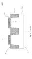
- the nitrogen-introducing resist film 19 (for example, about 300 nm thick) is patterned by normal lithography (for example, ArF lithography). Using the patterned nitrogen-introducing resist film 19 as an ion implantation mask, nitrogen is ion-implanted into the surface of the STI region 3 corresponding to the N-channel device region Rn, so that the nitrogen-introducing region 3n (N channel threshold adjusting element outward) A diffusion prevention region) is formed.
- ion implantation conditions for example, ion species: nitrogen, implantation energy: about 15 KeV, dose amount: 5 ⁇ 10 14 / cm 2 or the like (for example, implantation energy: about 5 to 30 KeV, dose amount: 5 ⁇ 10 13 / Cm 2 to 5 ⁇ 10 15 / cm 2 etc.) can be exemplified as a suitable one.
- ion implantation of nitrogen or the like is performed in the state where the silicon nitride film 11 for forming the STI and the pad silicon oxide film 12 are present, it is possible to prevent undesired introduction of nitrogen or the like into the N channel active region 4n. There is a merit that can be.
- the unnecessary nitrogen-introducing resist film 19 is removed by, for example, ashing.
- the silicon nitride film 11 for forming the STI is removed by, for example, hot phosphoric acid, and the device surface 1a of the wafer 1 is etched back by using, for example, a hydrofluoric acid-based etchant, whereby the pad silicon oxide film 12 is obtained. When these are removed, the result is as shown in FIG.
- the gate-first (Gate First) method has been mainly described as an example in the above-described embodiment, but the present invention is not limited thereto, and the gate-last (Gate Last) is described. It goes without saying that it can also be applied to the method.
- the present invention can be widely applied to a threshold voltage control technique in a semiconductor integrated circuit device and a method for manufacturing a semiconductor integrated circuit device (or a semiconductor device).
Landscapes
- Metal-Oxide And Bipolar Metal-Oxide Semiconductor Integrated Circuits (AREA)
- Semiconductor Memories (AREA)
- Insulated Gate Type Field-Effect Transistor (AREA)
Abstract
Description
先ず、本願において開示される発明の代表的な実施の形態について概要を説明する。
(a)半導体基板の第1の主面の表面に設けられた素子分離領域;
(b)前記半導体基板の前記第1の主面の前記表面に設けられ、前記素子分離領域によって相互に分離されたNチャネルアクティブ領域およびPチャネルアクティブ領域;
(c)前記半導体基板の前記第1の主面上に設けられ、前記Nチャネルアクティブ領域を横断し、Nチャネル型MISFETを構成するNチャネルゲートスタック;
(d)前記半導体基板の前記第1の主面上に設けられ、前記Pチャネルアクティブ領域を横断し、Pチャネル型MISFETを構成するPチャネルゲートスタック;
(e)前記Nチャネルゲートスタック下およびその周辺の前記素子分離領域の表面領域に設けられたNチャネル閾値調整元素外方拡散防止領域。
(a)半導体ウエハの第1の主面の表面に素子分離領域を形成することにより、前記半導体基板の前記第1の主面の前記表面に、Nチャネルアクティブ領域およびPチャネルアクティブ領域を区画する工程;
(b)前記半導体基板の前記第1の主面上に、前記Nチャネルアクティブ領域を横断し、Nチャネル型MISFETを構成するNチャネルゲートスタック(真性ゲートスタックおよびダミーゲートスタックを含む)を形成する工程;
(c)前記半導体基板の前記第1の主面上に、前記Pチャネルアクティブ領域を横断し、Pチャネル型MISFETを構成するPチャネルゲートスタックを形成する工程;
(d)前記工程(b)および(c)の前であって、前記工程(a)の後に、前記Nチャネルゲートスタック下およびその周辺の前記素子分離領域の表面領域に、Nチャネル閾値調整元素外方拡散防止領域を形成する工程。
1.本願において、実施の態様の記載は、必要に応じて、便宜上複数のセクションに分けて記載する場合もあるが、特にそうでない旨明示した場合を除き、これらは相互に独立別個のものではなく、単一の例の各部分、一方が他方の一部詳細または一部または全部の変形例等である。また、原則として、同様の部分は繰り返しを省略する。また、実施の態様における各構成要素は、特にそうでない旨明示した場合、理論的にその数に限定される場合および文脈から明らかにそうでない場合を除き、必須のものではない。
実施の形態について更に詳述する。各図中において、同一または同様の部分は同一または類似の記号または参照番号で示し、説明は原則として繰り返さない。
以下の例では、32nmテクノロジノードのCMIS半導体集積回路装置を例に取り具体的に説明するが、
これよりも微細な製品およびこれよりも寸法の大きな製品にも適用できることは言うまでもない。
このセクションでは、セクション1で説明したデバイス構造を実現するための要部プロセスを説明する。以下の説明では、主に、ゲートスタックのパターニングまでを説明する。これは、ゲートスタックのパターニング後のゲート側面構造体等を含むゲート構造体の形成およびソースドレイン領域の導入等は、ゲートファースト方式またはゲートラスト方式の選択も含めて、採用するプロセス方式によって、必要に応じて種々選択できるからである。
セクション2では、セクション1のデバイス構造を実現するデバイスの製法として、ランタン等のNチャネル閾値調整元素をイオン注入する方法を説明したが、このセクションでは、その変形例として、Nチャネル閾値調整元素含有膜からNチャネル閾値調整元素を導入する方法を説明する。いうまでもないことであるが、セクション2の方法を併用することを排除するものではない。
このセクションに於いては、セクション3と同様に、Nチャネル閾値調整元素含有膜成膜方式ではあるが、Nチャネル閾値調整元素導入領域3dを、Nチャネルデバイス領域Rnに対応する素子分離領域3の表面の内、Nチャネルアクティブ領域4nに近接した領域のみに限定することができるNチャネル閾値調整元素含有膜成膜&サイドウォール方式を説明する。
このセクションで説明する例は、セクション3で説明した製法の変形例で、ランタン等の選択的導入のために、ハードマスクを利用するところが特徴となっている。このは、たとえば、SRAM(Static Random Access Memory)等のように段差の激しい製品の加工に有利である。
このセクションでは、セクション1で説明したデバイス構造の変形例を説明する。セクション1の例では、Nチャネル閾値調整元素外方拡散防止領域として、Nチャネル閾値調整元素導入領域3d(図1から図3)を使用しているが、このセクションの例では、その代わりに、窒素導入領域3n(図27から図29)を使用している。
このセクションでは、セクション6で説明したデバイス構造を実現するための製造方法の一例を説明する。
以上本発明者によってなされた発明を実施形態に基づいて具体的に説明したが、本発明はそれに限定されるものではなく、その要旨を逸脱しない範囲において種々変更可能であることは言うまでもない。
1a (ウエハ又はチップの)表側主面(デバイス面)
1b (ウエハ又はチップの)裏側主面
1s (ウエハ又はチップの)基板部(P型単結晶シリコン基板部)
2 半導体チップ
3 STI領域(素子分離領域)
3d Nチャネル閾値調整元素導入領域(Nチャネル閾値調整元素外方拡散防止領域)
3n 窒素導入領域(Nチャネル閾値調整元素外方拡散防止領域)
3u Nチャネル閾値調整元素等非導入領域
4n Nチャネルアクティブ領域
4p Pチャネルアクティブ領域
5n Nチャネルゲートスタック
5p Pチャネルゲートスタック
6n N型ウエル領域
6p P型ウエル領域
7 IL(界面酸化シリコン系絶縁膜)
8 High-kゲート絶縁膜(酸化ハフニウム系High-kゲート絶縁膜)
8n NチャネルHigh-kゲート絶縁膜(ランタン添加酸化ハフニウム系High-kゲート絶縁膜)
8p PチャネルHigh-kゲート絶縁膜(アルミニウム添加酸化ハフニウム系High-kゲート絶縁膜)
9m メタルゲート電極膜(TiN膜)
9s ポリシリコンゲート電極膜
10n Nチャネル閾値調整膜(酸化ランタン膜)
10p Pチャネル閾値調整膜(アルミナ膜)
11 STI形成用窒化シリコン膜
12 パッド酸化シリコン膜
14 Nチャネル閾値調整元素導入用レジスト膜
15 Pチャネル閾値調整膜加工用ハードマスク膜(TiN膜)
16 Pチャネル閾値調整膜加工用ハードマスク用レジスト膜
17 Nチャネル閾値調整元素含有膜(酸化ランタン膜)
17s Nチャネル閾値調整元素含有膜サイドウォール
18 Nチャネル閾値調整元素含有膜加工用レジスト膜
19 窒素導入用レジスト膜
20n N型ソースドレイン領域
20p P型ソースドレイン領域
25 Pチャネルデバイス領域被覆用ハードマスク膜(TiN膜)
26 Pチャネルデバイス領域被覆ハードマスク加工用レジスト膜
Qn Nチャネル型MISFET
Qp Pチャネル型MISFET
Rn Nチャネルデバイス領域
Rp Pチャネルデバイス領域
Claims (11)
- 以下を含む半導体集積回路装置:
(a)半導体基板の第1の主面の表面に設けられた素子分離領域;
(b)前記半導体基板の前記第1の主面の前記表面に設けられ、前記素子分離領域によって相互に分離されたNチャネルアクティブ領域およびPチャネルアクティブ領域;
(c)前記半導体基板の前記第1の主面上に設けられ、前記Nチャネルアクティブ領域を横断し、Nチャネル型MISFETを構成するNチャネルゲートスタック;
(d)前記半導体基板の前記第1の主面上に設けられ、前記Pチャネルアクティブ領域を横断し、Pチャネル型MISFETを構成するPチャネルゲートスタック;
(e)前記Nチャネルゲートスタック下およびその周辺の前記素子分離領域の表面領域に設けられたNチャネル閾値調整元素外方拡散防止領域。 - 前記1項の半導体集積回路装置において、前記Nチャネル閾値調整元素外方拡散防止領域には、Nチャネル閾値調整元素がドープされている。
- 前記2項の半導体集積回路装置において、前記Nチャネル閾値調整元素は、La,Y,MgまたはScである。
- 前記1項の半導体集積回路装置において、前記Nチャネル閾値調整元素外方拡散防止領域には、窒素がドープされている。
- 前記3項の半導体集積回路装置において、前記Pチャネルゲートスタック下およびその周辺の前記素子分離領域の表面領域には、前記Nチャネル閾値調整元素外方拡散防止領域は設けられていない。
- 以下の工程を含む半導体集積回路装置の製造方法:
(a)半導体ウエハの第1の主面の表面に素子分離領域を形成することにより、前記半導体基板の前記第1の主面の前記表面に、Nチャネルアクティブ領域およびPチャネルアクティブ領域を区画する工程;
(b)前記半導体基板の前記第1の主面上に、前記Nチャネルアクティブ領域を横断し、Nチャネル型MISFETを構成するNチャネルゲートスタックを形成する工程;
(c)前記半導体基板の前記第1の主面上に、前記Pチャネルアクティブ領域を横断し、Pチャネル型MISFETを構成するPチャネルゲートスタックを形成する工程;
(d)前記工程(b)および(c)の前であって、前記工程(a)の後に、前記Nチャネルゲートスタック下およびその周辺の前記素子分離領域の表面領域に、Nチャネル閾値調整元素外方拡散防止領域を形成する工程。 - 前記6項の半導体集積回路装置の製造方法において、前記Nチャネル閾値調整元素外方拡散防止領域の形成は、Nチャネル閾値調整元素をイオン注入することによって行われる。
- 前記6項の半導体集積回路装置の製造方法において、前記Nチャネル閾値調整元素外方拡散防止領域の形成は、窒素をイオン注入することによって行われる。
- 前記6項の半導体集積回路装置の製造方法において、前記Nチャネル閾値調整元素外方拡散防止領域の形成は、前記Nチャネル閾値調整元素外方拡散防止領域となるべき部分の前記素子分離領域の表面に、Nチャネル閾値調整元素または、その酸化物を成膜し、熱処理することによって行われる。
- 前記7項の半導体集積回路装置の製造方法において、前記Nチャネル閾値調整元素外方拡散防止領域の形成は、前記Pチャネルゲートスタック下およびその周辺の前記素子分離領域の表面領域には、前記Nチャネル閾値調整元素外方拡散防止領域が形成されないように行われる。
- 前記10項の半導体集積回路装置の製造方法において、前記Nチャネル閾値調整元素は、La,Y,MgまたはScである。
Priority Applications (2)
| Application Number | Priority Date | Filing Date | Title |
|---|---|---|---|
| JP2013509894A JP5684371B2 (ja) | 2011-04-14 | 2012-04-09 | 半導体集積回路装置の製造方法 |
| US14/111,549 US9287259B2 (en) | 2011-04-14 | 2012-04-09 | Semiconductor integrated circuit device and method for manufacturing semiconductor integrated circuit device |
Applications Claiming Priority (2)
| Application Number | Priority Date | Filing Date | Title |
|---|---|---|---|
| JP2011089693 | 2011-04-14 | ||
| JP2011-089693 | 2011-04-14 |
Publications (1)
| Publication Number | Publication Date |
|---|---|
| WO2012141122A1 true WO2012141122A1 (ja) | 2012-10-18 |
Family
ID=47009295
Family Applications (1)
| Application Number | Title | Priority Date | Filing Date |
|---|---|---|---|
| PCT/JP2012/059642 Ceased WO2012141122A1 (ja) | 2011-04-14 | 2012-04-09 | 半導体集積回路装置および半導体集積回路装置の製造方法 |
Country Status (3)
| Country | Link |
|---|---|
| US (1) | US9287259B2 (ja) |
| JP (1) | JP5684371B2 (ja) |
| WO (1) | WO2012141122A1 (ja) |
Cited By (1)
| Publication number | Priority date | Publication date | Assignee | Title |
|---|---|---|---|---|
| CN110970428A (zh) * | 2018-09-28 | 2020-04-07 | 台湾积体电路制造股份有限公司 | 集成电路 |
Families Citing this family (4)
| Publication number | Priority date | Publication date | Assignee | Title |
|---|---|---|---|---|
| US20140103452A1 (en) * | 2012-10-15 | 2014-04-17 | Marvell World Trade Ltd. | Isolation components for transistors formed on fin features of semiconductor substrates |
| KR102532497B1 (ko) | 2016-09-19 | 2023-05-17 | 삼성전자주식회사 | 반도체 소자 및 이의 제조 방법 |
| US10340343B2 (en) | 2017-10-31 | 2019-07-02 | Taiwan Semiconductor Manufacturing Company Ltd. | Semiconductor device and method for manufacturing the same |
| US11222782B2 (en) * | 2020-01-17 | 2022-01-11 | Microchip Technology Inc. | Self-aligned implants for silicon carbide (SiC) technologies and fabrication method |
Citations (6)
| Publication number | Priority date | Publication date | Assignee | Title |
|---|---|---|---|---|
| JP2005333060A (ja) * | 2004-05-21 | 2005-12-02 | Seiko Epson Corp | 半導体装置および半導体装置の製造方法 |
| JP2008235351A (ja) * | 2007-03-16 | 2008-10-02 | Seiko Epson Corp | 半導体装置の製造方法及び半導体装置。 |
| JP2009194352A (ja) * | 2008-01-17 | 2009-08-27 | Toshiba Corp | 半導体装置の製造方法 |
| JP2010205917A (ja) * | 2009-03-03 | 2010-09-16 | Panasonic Corp | 半導体装置 |
| JP2011009373A (ja) * | 2009-06-24 | 2011-01-13 | Renesas Electronics Corp | 半導体装置の製造方法および半導体装置 |
| JP2012038800A (ja) * | 2010-08-04 | 2012-02-23 | Panasonic Corp | 半導体装置及びその製造方法 |
Family Cites Families (13)
| Publication number | Priority date | Publication date | Assignee | Title |
|---|---|---|---|---|
| JP2000082808A (ja) * | 1998-09-04 | 2000-03-21 | Toshiba Corp | 半導体装置及びその製造方法 |
| JP2003017555A (ja) * | 2001-06-29 | 2003-01-17 | Hitachi Ltd | 半導体集積回路装置およびその製造方法 |
| JP2003179157A (ja) * | 2001-12-10 | 2003-06-27 | Nec Corp | Mos型半導体装置 |
| US6734082B2 (en) * | 2002-08-06 | 2004-05-11 | Chartered Semiconductor Manufacturing Ltd. | Method of forming a shallow trench isolation structure featuring a group of insulator liner layers located on the surfaces of a shallow trench shape |
| US20040164373A1 (en) * | 2003-02-25 | 2004-08-26 | Koester Steven John | Shallow trench isolation structure for strained Si on SiGe |
| US20060267130A1 (en) * | 2003-06-26 | 2006-11-30 | Rj Mears, Llc | Semiconductor Device Including Shallow Trench Isolation (STI) Regions with a Superlattice Therebetween |
| US7514328B2 (en) * | 2003-06-26 | 2009-04-07 | Mears Technologies, Inc. | Method for making a semiconductor device including shallow trench isolation (STI) regions with a superlattice therebetween |
| US7812339B2 (en) * | 2007-04-23 | 2010-10-12 | Mears Technologies, Inc. | Method for making a semiconductor device including shallow trench isolation (STI) regions with maskless superlattice deposition following STI formation and related structures |
| US7615840B2 (en) * | 2007-06-21 | 2009-11-10 | Infineon Technologies Ag | Device performance improvement using flowfill as material for isolation structures |
| US8216913B2 (en) * | 2007-12-24 | 2012-07-10 | Texas Instruments Incorporated | Strain modulation in active areas by controlled incorporation of nitrogen at si-SiO2 interface |
| US8034678B2 (en) * | 2008-01-17 | 2011-10-11 | Kabushiki Kaisha Toshiba | Complementary metal oxide semiconductor device fabrication method |
| US8222093B2 (en) * | 2010-02-17 | 2012-07-17 | GlobalFoundries, Inc. | Methods for forming barrier regions within regions of insulating material resulting in outgassing paths from the insulating material and related devices |
| US9543188B2 (en) * | 2010-11-09 | 2017-01-10 | Institute Of Microelectonics, Chinese Academy Of Sciences | Isolation structure, method for manufacturing the same, and semiconductor device having the structure |
-
2012
- 2012-04-09 WO PCT/JP2012/059642 patent/WO2012141122A1/ja not_active Ceased
- 2012-04-09 US US14/111,549 patent/US9287259B2/en not_active Expired - Fee Related
- 2012-04-09 JP JP2013509894A patent/JP5684371B2/ja not_active Expired - Fee Related
Patent Citations (6)
| Publication number | Priority date | Publication date | Assignee | Title |
|---|---|---|---|---|
| JP2005333060A (ja) * | 2004-05-21 | 2005-12-02 | Seiko Epson Corp | 半導体装置および半導体装置の製造方法 |
| JP2008235351A (ja) * | 2007-03-16 | 2008-10-02 | Seiko Epson Corp | 半導体装置の製造方法及び半導体装置。 |
| JP2009194352A (ja) * | 2008-01-17 | 2009-08-27 | Toshiba Corp | 半導体装置の製造方法 |
| JP2010205917A (ja) * | 2009-03-03 | 2010-09-16 | Panasonic Corp | 半導体装置 |
| JP2011009373A (ja) * | 2009-06-24 | 2011-01-13 | Renesas Electronics Corp | 半導体装置の製造方法および半導体装置 |
| JP2012038800A (ja) * | 2010-08-04 | 2012-02-23 | Panasonic Corp | 半導体装置及びその製造方法 |
Cited By (3)
| Publication number | Priority date | Publication date | Assignee | Title |
|---|---|---|---|---|
| CN110970428A (zh) * | 2018-09-28 | 2020-04-07 | 台湾积体电路制造股份有限公司 | 集成电路 |
| US12199086B2 (en) | 2018-09-28 | 2025-01-14 | Taiwan Semiconductor Manufacturing Company, Ltd. | Stack-gate circuit |
| US12349469B2 (en) | 2018-09-28 | 2025-07-01 | Taiwan Semiconductor Manufacturing Company, Ltd. | Stack-gate circuit |
Also Published As
| Publication number | Publication date |
|---|---|
| JP5684371B2 (ja) | 2015-03-11 |
| US20140035055A1 (en) | 2014-02-06 |
| JPWO2012141122A1 (ja) | 2014-07-28 |
| US9287259B2 (en) | 2016-03-15 |
Similar Documents
| Publication | Publication Date | Title |
|---|---|---|
| JP5661445B2 (ja) | 半導体集積回路装置およびその製造方法 | |
| US9111906B2 (en) | Method for fabricating semiconductor device having spacer elements | |
| CN102117774B (zh) | 集成电路元件的形成方法 | |
| US10134731B2 (en) | Dielectric liner added after contact etch before silicide formation | |
| CN103137624B (zh) | 高栅极密度器件和方法 | |
| CN102103995B (zh) | 集成电路元件的形成方法 | |
| US8652955B2 (en) | Manufacturing method of semiconductor integrated circuit device | |
| US8372706B2 (en) | Semiconductor device fabrication method including hard mask and sacrificial spacer elements | |
| US8536005B2 (en) | Semiconductor integrated circuit device and manufacturing method thereof | |
| US20120252180A1 (en) | Manufacturing method of semiconductor integrated circuit device | |
| US20130200466A1 (en) | Integrated circuit having silicide block resistor | |
| TW202211373A (zh) | 半導體結構及其形成方法 | |
| JP5684371B2 (ja) | 半導体集積回路装置の製造方法 | |
| CN104795362B (zh) | 一种制作半导体器件的方法 | |
| US8513742B2 (en) | Method for manufacturing contact and semiconductor device having said contact | |
| JP2012129291A (ja) | 半導体集積回路装置 | |
| JP2012209332A (ja) | 半導体集積回路装置の製造方法 | |
| TW202326935A (zh) | 製造半導體裝置的方法及半導體裝置 | |
| JP2010272597A (ja) | 半導体装置およびその製造方法 | |
| JP2012256659A (ja) | 半導体集積回路装置の製造方法 |
Legal Events
| Date | Code | Title | Description |
|---|---|---|---|
| 121 | Ep: the epo has been informed by wipo that ep was designated in this application |
Ref document number: 12771644 Country of ref document: EP Kind code of ref document: A1 |
|
| ENP | Entry into the national phase |
Ref document number: 2013509894 Country of ref document: JP Kind code of ref document: A |
|
| WWE | Wipo information: entry into national phase |
Ref document number: 14111549 Country of ref document: US |
|
| NENP | Non-entry into the national phase |
Ref country code: DE |
|
| 122 | Ep: pct application non-entry in european phase |
Ref document number: 12771644 Country of ref document: EP Kind code of ref document: A1 |