WO2012140765A1 - 光学素子、ヘッドアップディスプレイ及び光源ユニット - Google Patents
光学素子、ヘッドアップディスプレイ及び光源ユニット Download PDFInfo
- Publication number
- WO2012140765A1 WO2012140765A1 PCT/JP2011/059281 JP2011059281W WO2012140765A1 WO 2012140765 A1 WO2012140765 A1 WO 2012140765A1 JP 2011059281 W JP2011059281 W JP 2011059281W WO 2012140765 A1 WO2012140765 A1 WO 2012140765A1
- Authority
- WO
- WIPO (PCT)
- Prior art keywords
- microlens array
- microlens
- lens
- microlenses
- optical element
- Prior art date
- Legal status (The legal status is an assumption and is not a legal conclusion. Google has not performed a legal analysis and makes no representation as to the accuracy of the status listed.)
- Ceased
Links
Images







Classifications
-
- G—PHYSICS
- G02—OPTICS
- G02B—OPTICAL ELEMENTS, SYSTEMS OR APPARATUS
- G02B3/00—Simple or compound lenses
- G02B3/0006—Arrays
- G02B3/0037—Arrays characterized by the distribution or form of lenses
- G02B3/005—Arrays characterized by the distribution or form of lenses arranged along a single direction only, e.g. lenticular sheets
-
- G—PHYSICS
- G02—OPTICS
- G02B—OPTICAL ELEMENTS, SYSTEMS OR APPARATUS
- G02B27/00—Optical systems or apparatus not provided for by any of the groups G02B1/00 - G02B26/00, G02B30/00
- G02B27/01—Head-up displays
- G02B27/0101—Head-up displays characterised by optical features
-
- G—PHYSICS
- G02—OPTICS
- G02B—OPTICAL ELEMENTS, SYSTEMS OR APPARATUS
- G02B3/00—Simple or compound lenses
- G02B3/0006—Arrays
- G02B3/0037—Arrays characterized by the distribution or form of lenses
- G02B3/0056—Arrays characterized by the distribution or form of lenses arranged along two different directions in a plane, e.g. honeycomb arrangement of lenses
-
- G—PHYSICS
- G02—OPTICS
- G02B—OPTICAL ELEMENTS, SYSTEMS OR APPARATUS
- G02B27/00—Optical systems or apparatus not provided for by any of the groups G02B1/00 - G02B26/00, G02B30/00
- G02B27/01—Head-up displays
- G02B27/0101—Head-up displays characterised by optical features
- G02B2027/0118—Head-up displays characterised by optical features comprising devices for improving the contrast of the display / brillance control visibility
-
- G—PHYSICS
- G02—OPTICS
- G02B—OPTICAL ELEMENTS, SYSTEMS OR APPARATUS
- G02B27/00—Optical systems or apparatus not provided for by any of the groups G02B1/00 - G02B26/00, G02B30/00
- G02B27/48—Laser speckle optics
-
- G—PHYSICS
- G02—OPTICS
- G02B—OPTICAL ELEMENTS, SYSTEMS OR APPARATUS
- G02B3/00—Simple or compound lenses
- G02B3/0006—Arrays
Definitions
- the present invention relates to an optical element using a microlens array.
- Patent Document 1 proposes an image forming apparatus including a laser projector that uses a laser beam as a light source and projects an image formed by an array of a plurality of pixels, and a microlens array in which a plurality of microlenses are arrayed. Yes.
- a microlens array is used, incident light can be appropriately dispersed and a necessary diffusion angle can be freely designed.
- Patent Documents 2 and 3 and Non-Patent Document 1 propose that a screen is configured using two microlens arrays or two diffraction gratings.
- Non-Patent Document 1 there is a tendency that uneven brightness occurs when only one microlens array is used. However, such uneven brightness occurs when two microlens arrays are used. It is described that can be suppressed.
- an image (hereinafter referred to as “intermediate image”) is formed in which the focal point of each microlens included in the microlens array is a pixel position.
- the light source is a laser
- the condensing characteristic at the focal point of the microlens array is high. Therefore, in some cases, pixels formed by each microlens (that is, pixels corresponding to the focal point of the microlens) are separated on the intermediate image plane by the microlens array. In other words, a bright portion and a dark portion may appear prominently on the intermediate image plane.
- Patent Documents 1 to 3 and Non-Patent Document 1 described above do not describe a technique for suppressing such excessive pixel bright spots.
- An object of the present invention is to provide an optical element, a head-up display, and a light source unit that can appropriately suppress excessive pixel bright spots in a configuration using a microlens array.
- an optical element having a first microlens array part and a second microlens array part in which a plurality of microlenses are arranged, the first microlens array part and the second microlens array part.
- the lens array unit is disposed opposite to each other at positions spaced apart from each other by a distance longer than the focal length of the microlens arranged in the first microlens array unit, and the microarray arranged in the second microlens array unit.
- An interval between the lenses is configured to be narrower than an interval between the microlenses arranged in the first microlens array portion, and the first microlens array portion is light with respect to the second microlens array portion. It is arranged on the incident side.
- a head-up display includes the optical element according to any one of the first to sixteenth aspects, and an image formed by the optical element is visually recognized as a virtual image from the position of the user's eyes.
- the light source unit includes a light source, a first microlens array in which a plurality of microlenses are arranged at a predetermined interval, and a plurality of microlenses arranged at an interval narrower than the predetermined interval.
- a second microlens array wherein the second microlens array is disposed at a position separated by a distance longer than a focal length of a macro lens disposed in the first microlens array,
- One microlens array is disposed on the incident side of light emitted from the light source with respect to the second microlens array.
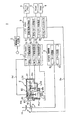
- the structure of the image display apparatus which concerns on a present Example is shown.
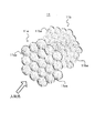
- the perspective view of the screen which concerns on a present Example is shown.
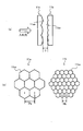
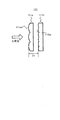
- the structure of the 1st and 2nd micro lens array part which concerns on a present Example is shown.
- the figure for demonstrating the excessive pixel luminescent spot which may be produced by the general micro lens array part is shown.
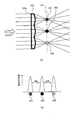
- action and effect of the screen which concerns on a present Example is shown.
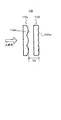
- the concrete structure of the screen which concerns on the modification 1 is shown.
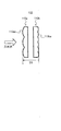
- the specific structure of the screen which concerns on the other example of the modification 1 is shown.
- the specific structure of the screen which concerns on the modification 2 is shown.
- the concrete structure of the screen which concerns on the modification 3 is shown.
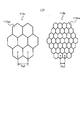
- the specific structure of the screen which concerns on the modification 4 is shown.
- the specific structure of the screen which concerns on the modification 5 is shown.
- the specific structure of the screen which concerns on the other example of the modification 5 is shown.
- the specific structure of the screen which concerns on the modification 6 is shown.
- the specific structure of the screen which concerns on the other example of the modification 6 is shown.
- the specific structure of the screen which concerns on the modification 7 is shown.
- the specific structure of the screen which concerns on the other example of the modification 7 is shown.
- the specific structure of the screen which concerns on the modification 8 is shown.
- the specific structure of the screen which concerns on the other example of the modification 8 is shown.
- an optical element having a first microlens array section and a second microlens array section in which a plurality of microlenses are arranged, the first microlens array section and the second microlens.
- the array unit is disposed opposite to each other at a position separated from each other by a distance longer than the focal length of the micro lens arranged in the first micro lens array unit, and the micro lens arranged in the second micro lens array unit
- the interval between each other is configured to be narrower than the interval between the microlenses arranged in the first microlens array unit, and the first microlens array unit transmits light to the second microlens array unit. It is arranged on the incident side.
- the above-described optical element has first and second microlens array portions each having a plurality of microlenses arranged therein.
- the optical element corresponds to a screen.
- the first and second microlens array units are arranged to face each other at positions separated from each other by a distance longer than the focal length of the microlenses arranged in the first microlens array unit.
- the first microlens array part is disposed on the light incident side with respect to the second microlens array part.
- the first and second microlens array units are configured such that the interval between the microlenses arranged in the second microlens array unit is narrower than the interval between the microlenses arranged in the first microlens array unit. ing.
- the lens pitch of the microlenses of the second microlens array portion is configured to be smaller than the lens pitch of the microlenses of the first microlens array portion.
- the lens diameter of one microlens of the second microlens array unit is configured to be smaller than the lens diameter of one microlens of the first microlens array unit.
- the light collected by one microlens of the first microlens array unit is incident on two or more microlenses of the second microlens array unit.
- one pixel formed by one microlens of the first microlens array unit is distributed by two or more microlenses of the second microlens array unit, and two or more pixels (distribution pixels) are obtained. It is formed.
- the intervals between the distribution pixels are equal to the lens pitch of the second microlens array unit that is smaller than the lens pitch of the first microlens array unit.
- the second microlens array part the light collection characteristic for each pixel is expanded.
- optical element it is possible to make pixel separation inconspicuous, that is, to make pixel luminescent spots inconspicuous. Therefore, according to the optical element, it is possible to appropriately suppress the occurrence of excessive pixel bright spots even when the intermediate image by the second microlens array unit is enlarged and displayed.
- light collected by one microlens of the first microlens array unit is distributed by being incident on two or more microlenses of the second microlens array unit.
- the interval between the microlenses arranged in the first microlens array portion and the second microlens array portion is set.
- the first light is collected so that the light collected by one microlens of the first microlens array unit is distributed by being incident on two or more microlenses of the second microlens array unit.
- An interval between the microlenses arranged in the microlens array unit and the second microlens array unit is set. Thereby, generation
- an interval between the microlenses arranged in the second microlens array unit is “1” which is an interval between the microlenses arranged in the first microlens array unit. / 2 "or less.
- the interval between the microlenses is an interval between centroids of adjacent microlenses.
- the interval between microlenses is the distance between the centers of adjacent microlenses.
- the first microlens array unit and the second microlens array unit are 1.5 times or more the focal length of the microlens arranged in the first microlens array unit, and Oppositely arranged at a position separated by a distance of three times or less.
- each of the plurality of microlenses is configured with a polygonal lens outline in a plan view, and the first microlens array unit and the second microlens array unit The angle between the apex direction of the lens outline of the microlens arranged in the first microlens array part and the apex direction of the lens outline of the microlens arranged in the second microlens array part are shifted. Has been.
- the first and second microlens array portions are arranged in a polygonal apex direction which is a lens contour of the microlens arranged in the first microlens array portion, and in the second microlens array portion.
- the angle difference from the apex direction of the polygonal shape that is the lens contour of the arranged microlenses is configured to a predetermined angle. That is, a plurality of microlenses are arranged in the first and second microlens array portions so that the polygonal shape that is the lens contour is rotated by a predetermined angle.
- optical element unnecessary interference due to a polygonal image that may occur on the incident surface can be suppressed, and the influence of the positional deviation in the first and second microlens array portions can be appropriately suppressed. It becomes. Further, according to the optical element described above, since it is not necessary to strictly adjust the positions of the first and second microlens array portions, it is possible to produce the optical element easily and at low cost.
- the polygonal shape is a regular hexagonal shape
- the apex direction of the lens contour of the microlens arranged in the first microlens array portion is approximately 30 degrees or approximately 90 degrees. According to this aspect, it is possible to effectively suppress the influence due to the displacement in the first and second microlens array portions.
- the polygonal shape is a square shape
- the apex direction of the lens contour of the microlens arranged in the first microlens array portion, and the second microlens array The angle difference between the microlenses arranged in the section and the apex direction of the lens contour is approximately 45 degrees or approximately 135 degrees. According to this aspect, it is possible to effectively suppress the influence due to the displacement in the first and second microlens array portions.
- each of the plurality of microlenses has a regular polygonal lens profile in plan view
- the first microlens array unit and the second microlens array unit are The angle between the apex direction of the lens outline of the microlens arranged in the first microlens array part and the apex direction of the lens outline of the microlens arranged in the second microlens array part, It is configured to be shifted by half of one interior angle included in the regular polygon shape. Also according to this aspect, it is possible to effectively suppress the influence of the positional deviation in the first and second microlens array portions.
- each of the first microlens array unit and the second microlens array unit includes the plurality of microlenses arranged at equal intervals, and the microlens is one microlens.
- the microlenses arranged adjacent to the apex of the one microlens at a predetermined angle, and arranged in the first microlens array unit, and arranged in the second microlens array unit
- the microlens is configured to be shifted from the one microlens by half the predetermined angle. Also according to this aspect, it is possible to effectively suppress the influence due to the displacement in the first and second microlens array portions.
- the optical element includes a first lens array having the first microlens array portion on one surface and a second lens array having the second microlens array portion on one surface. Is done.
- the first and second microlens array units are configured separately, and a plurality of microlenses are formed on one side of each.
- the first microlens array part and the second microlens array part are formed on opposing surfaces of the first lens array and the second lens array, respectively.
- each of the first and second microlens array units has a plurality of microlenses formed on the opposing surfaces of the first and second microlens array units.
- the first microlens array portion is formed on a surface of the first lens array that does not face the surface of the second lens array on which the second microlens array portion is formed. ing.
- one of the first and second microlens array units has a plurality of microlenses formed on opposing surfaces of the first and second microlens array units, and the first and second microlens array units.
- the other has a plurality of microlenses formed on the surface opposite to the opposing surface.
- first microlens array part and the second microlens array part are formed on surfaces of the first lens array and the second lens array that are not opposed to each other.
- each of the first and second microlens array units has a plurality of microlenses formed on the surface opposite to the opposing surface of the first and second microlens array units.
- the first microlens array portion is provided on one surface, and the second microlens array portion is provided on the other surface.
- the first and second microlens array portions are integrally formed, and a plurality of microlenses are formed on opposite surfaces of the optical element. According to this aspect, since the two microlens array portions are integrally formed, it is only necessary to create one component on which the microlens array is formed, thereby further reducing the cost required for the optical element. It becomes possible.
- the above-described optical element can be suitably applied to a head-up display that visually recognizes an image as a virtual image from the position of the user's eyes.
- the light source unit includes a light source, a first microlens array in which a plurality of microlenses are arranged at a predetermined interval, and a plurality of microlenses arranged at an interval narrower than the predetermined interval.
- a second microlens array wherein the second microlens array is disposed at a position separated by a distance longer than a focal length of a macro lens disposed in the first microlens array,
- the microlens array is disposed on the incident side of the light emitted from the light source with respect to the second microlens array.
- FIG. 1 shows a configuration of an image display device to which an optical element according to the present embodiment is applied.
- the image display device 1 includes an image signal input unit 2, a video ASIC 3, a frame memory 4, a ROM 5, a RAM 6, a laser driver ASIC 7, a MEMS control unit 8, and a laser light source unit 9.
- the image display device 1 is applied to, for example, a head-up display.
- the head-up display is a device that visually recognizes an image as a virtual image from the position (eye point) of the driver's eyes.
- the image signal input unit 2 receives an image signal input from the outside and outputs it to the video ASIC 3.
- the video ASIC 3 is a block that controls the laser driver ASIC 7 and the MEMS control unit 8 based on the image signal input from the image signal input unit 2 and the scanning position information Sc input from the MEMS mirror 10, and is ASIC (Application Specific Integrated). Circuit).
- the video ASIC 3 includes a synchronization / image separation unit 31, a bit data conversion unit 32, a light emission pattern conversion unit 33, and a timing controller 34.
- the synchronization / image separation unit 31 separates the image data displayed on the screen as the image display unit and the synchronization signal from the image signal input from the image signal input unit 2 and writes the image data to the frame memory 4.
- the bit data conversion unit 32 reads the image data written in the frame memory 4 and converts it into bit data.
- the light emission pattern conversion unit 33 converts the bit data converted by the bit data conversion unit 32 into a signal representing the light emission pattern of each laser.
- the timing controller 34 controls the operation timing of the synchronization / image separation unit 31 and the bit data conversion unit 32.
- the timing controller 34 also controls the operation timing of the MEMS control unit 8 described later.
- the image data separated by the synchronization / image separation unit 31 is written.
- the ROM 5 stores a control program and data for operating the video ASIC 3. Various data are sequentially read from and written into the RAM 6 as a work memory when the video ASIC 3 operates.
- the laser driver ASIC 7 is a block that generates a signal for driving a laser diode provided in a laser light source unit 9 described later, and is configured as an ASIC.
- the laser driver ASIC 7 includes a red laser driving circuit 71, a blue laser driving circuit 72, and a green laser driving circuit 73.
- the red laser driving circuit 71 drives the red laser LD1 based on the signal output from the light emission pattern conversion unit 33.
- the blue laser drive circuit 72 drives the blue laser LD2 based on the signal output from the light emission pattern conversion unit 33.
- the green laser drive circuit 73 drives the green laser LD3 based on the signal output from the light emission pattern conversion unit 33.
- the MEMS control unit 8 controls the MEMS mirror 10 based on a signal output from the timing controller 34.
- the MEMS control unit 8 includes a servo circuit 81 and a driver circuit 82.
- the servo circuit 81 controls the operation of the MEMS mirror 10 based on a signal from the timing controller.
- the driver circuit 82 amplifies the control signal of the MEMS mirror 10 output from the servo circuit 81 to a predetermined level and outputs the amplified signal.
- the laser light source unit 9 emits laser light to the MEMS mirror 10 based on the drive signal output from the laser driver ASIC 7.
- the MEMS mirror 10 as a scanning unit reflects the laser light emitted from the laser light source unit 9 toward the screen 11. In this way, the MEMS mirror 10 forms an image to be displayed on the screen 11.
- the MEMS mirror 10 moves so as to scan on the screen 11 under the control of the MEMS control unit 8 in order to display the image input to the image signal input unit 2, and the scanning position information (for example, information such as a mirror angle) is output to the video ASIC 3.
- the screen 11 is an example of the “optical element” according to the present invention, is configured as a transmissive screen, and includes a microlens array unit (not shown) in which a plurality of microlenses are arranged.
- the microlens array unit appropriately disperses incident light. Specifically, the microlens array unit diffuses light at a diffusion angle corresponding to the curvature of the lens.
- the curvature of the lens in the microlens array unit is designed in advance according to the required diffusion angle. Details of the screen 11 will be described later.
- the image display device 1 actually displays an image corresponding to the light emitted from the screen 11 as described above, the light reflected by the reflecting mirror (combiner), the light enlarged by the magnifying element, and the like. It is visually recognized as a virtual image from the driver's eye position (eye point).
- the laser light source unit 9 includes a case 91, a wavelength selective element 92, a collimator lens 93, a red laser LD1, a blue laser LD2, a green laser LD3, a monitor light receiving element (hereinafter simply referred to as “light receiving element”). 50).
- the case 91 is formed in a substantially box shape with resin or the like.
- the case 91 is provided with a hole penetrating into the case 91 and a CAN attachment portion 91a having a concave cross section, and a surface perpendicular to the CAN attachment portion 91a. A hole penetrating inward is formed, and a collimator mounting portion 91b having a concave cross section is formed.
- the wavelength-selective element 92 as a combining element is configured by, for example, a trichroic prism, and is provided with a reflective surface 92a and a reflective surface 92b.
- the reflection surface 92a transmits the laser light emitted from the red laser LD1 toward the collimator lens 93, and reflects the laser light emitted from the blue laser LD2 toward the collimator lens 93.
- the reflecting surface 92b transmits most of the laser light emitted from the red laser LD1 and the blue laser LD2 toward the collimator lens 93 and reflects a part thereof toward the light receiving element 50.
- the reflection surface 92 b reflects most of the laser light emitted from the green laser LD 3 toward the collimator lens 93 and transmits part of the laser light toward the light receiving element 50. In this way, the emitted light from each laser is superimposed and incident on the collimator lens 93 and the light receiving element 50.
- the wavelength selective element 92 is provided in the vicinity of the collimator mounting portion 91b in the case 91.
- the collimator lens 93 emits the laser beam incident from the wavelength selective element 92 to the MEMS mirror 10 as parallel light.
- the collimator lens 93 is fixed to the collimator mounting portion 91b of the case 91 with a UV adhesive or the like. That is, the collimator lens 93 is provided after the synthesis element.
- the red laser LD1 as a laser light source emits red laser light.
- the red laser LD1 is fixed at a position that is coaxial with the wavelength selective element 92 and the collimator lens 93 in the case 91 while the semiconductor laser light source is in the chip state or the chip is mounted on a submount or the like. ing.
- Blue laser LD2 as a laser light source emits blue laser light.
- the blue laser LD2 is fixed at a position where the emitted laser light can be reflected toward the collimator lens 93 by the reflecting surface 92a while the semiconductor laser light source is in the chip state or the chip is mounted on the submount or the like. ing.
- the positions of the red laser LD1 and the blue laser LD2 may be switched.
- the green laser LD3 as a laser light source is attached to the CAN package or attached to the frame package, and emits green laser light.
- the green laser LD 3 has a semiconductor laser light source chip B that generates green laser light in a CAN package, and is fixed to a CAN mounting portion 91 a of the case 91.
- the light receiving element 50 receives a part of the laser light emitted from each laser light source.
- the light receiving element 50 is a photoelectric conversion element such as a photodetector, and supplies a detection signal Sd, which is an electrical signal corresponding to the amount of incident laser light, to the laser driver ASIC 7.
- a detection signal Sd which is an electrical signal corresponding to the amount of incident laser light
- the laser driver ASIC 7 adjusts the power of the red laser LD1, the blue laser LD2, and the green laser LD3 according to the detection signal Sd.
- the laser driver ASIC 7 operates only the red laser driving circuit 71, supplies a driving current to the red laser LD1, and emits red laser light from the red laser LD1. A part of the red laser light is received by the light receiving element 50, and a detection signal Sd corresponding to the amount of light is fed back to the laser driver ASIC7.
- the laser driver ASIC 7 adjusts the drive current supplied from the red laser drive circuit 71 to the red laser LD1 so that the light amount indicated by the detection signal Sd is an appropriate light amount. In this way, power adjustment is performed.
- the power adjustment of the blue laser LD2 and the power adjustment of the green laser LD3 are similarly performed.
- the above-described configuration unit including at least the laser light source unit 9 and the screen 11 corresponds to an example of the “light source unit” according to the present invention.
- the screen 11 is an example of the “optical element” according to the present invention.
- FIG. 2 is a perspective view of the screen 11 according to the present embodiment.
- the screen 11 includes a first microlens array part 11 a and a second microlens array part 11 b that are opposed to each other with a predetermined distance therebetween.
- the first microlens array part 11a and the second microlens array part 11b are each configured in a substantially disc shape.
- each of the first microlens array unit 11a and the second microlens array unit 11b includes a plurality of microlenses 11aa and 11ba each having a regular hexagonal lens outline in a plan view in a lattice shape on one side. Is formed.
- the first microlens array portion 11a is disposed on the incident light side, and the second microlens array portion 11b is disposed on the outgoing light side. That is, the light first enters the first microlens array unit 11a, and the light emitted from the first microlens array unit 11a enters the second microlens array unit 11b.
- FIG. 3 is a diagram illustrating a specific configuration of the first microlens array unit 11a and the second microlens array unit 11b according to the present embodiment.
- FIG. 3A is a cross-sectional view of the first microlens array unit 11a and the second microlens array unit 11b taken along a plane perpendicular to the light traveling direction. Specifically, a cross-sectional view showing a part of the first microlens array portion 11a and the second microlens array portion 11b in an enlarged manner is shown. As shown in FIG.
- the first microlens array portion 11a and the second microlens array portion 11b are arranged to face each other so that the surfaces on which the plurality of microlenses 11aa and 11ba are formed face each other. That is, the first microlens array portion 11a and the second microlens array portion 11b are formed with a plurality of microlenses 11aa and 11ba on the opposing surfaces, respectively. Further, the first microlens array unit 11a and the second microlens array unit 11b are arranged to face each other at a position separated by a distance D.
- the first microlens array unit 11a and the second microlens array unit 11b are arranged at positions separated by a distance D that is at least longer than the focal length of the microlenses 11aa arranged in the first microlens array unit 11a. Place them facing each other.
- the first microlens array unit 11a and the second microlens array unit 11b are arranged at positions separated by a distance D that is 1.5 to 3 times the focal length of the microlens 11aa.
- FIG. 3B is a plan view of the first microlens array unit 11a and the second microlens array unit 11b. Specifically, the top view which expanded and represented a part of 1st micro lens array part 11a and the 2nd micro lens array part 11b observed from the direction along the advancing direction of light is shown.
- each of the first microlens array unit 11a and the second microlens array unit 11b includes a plurality of microlenses 11aa and 11ba each having a regular hexagonal lens profile in plan view. Are arranged in a grid pattern. Specifically, the plurality of microlenses 11aa and 11ba are arranged with adjacent sides forming a regular hexagonal shape.
- the first microlens array unit 11a and the second microlens array unit 11b are configured so that the lens pitch Pb is different.
- the lens diameter Pb in the second microlens array unit 11b is smaller than the lens pitch Pa in the first microlens array unit 11a, in other words, the lens diameter of one microlens 11ba is one microlens.
- the first microlens array unit 11a and the second microlens array unit 11b are configured to be smaller than the lens diameter of 11aa.
- the first microlens array unit 11a and the second microlens array unit 11b are configured so that the lens pitch Pb of the microlens 11ba is equal to or less than “1 ⁇ 2” of the lens pitch Pa of the microlens 11aa.
- the lens pitches Pa and Pb described above are, in other words, intervals between adjacent microlenses 11aa and 11ba arranged in the first microlens array unit 11a and the second microlens array unit 11b, and adjacent microlenses 11aa. , 11ba, which corresponds to the distance between the centers of gravity (that is, the distance between the centers). The same shall apply hereinafter.
- FIG. 4A shows a diagram for explaining an intermediate image formed by a general microlens array unit 200.
- an intermediate image having a focal point of each microlens 200a of the microlens array unit 200 as a pixel position is a surface indicated by reference numeral 201 (a focal plane, hereinafter “ Called an "intermediate image plane”).
- the intermediate image is composed of pixels 202, 203, and 204 formed at the focal position of the microlens 200a.
- Such an interval between the pixels 202, 203, and 204 is equal to the lens pitch Pa of the microlens array unit 200.
- FIG. 4B shows a luminance intensity distribution on the intermediate image plane 201. Specifically, the luminance intensity distribution (generally Gaussian distribution) corresponding to the pixels 202, 203, and 204 formed on the intermediate image plane 201 is shown.
- the luminance intensity distribution generally Gaussian distribution
- the intermediate image plane 201 tends to be in a state where the pixels 202, 203, and 204 are separated. That is, in the intermediate image plane 201, a bright portion and a dark portion tend to appear remarkably.
- the pixels 202, 203, and 204 formed by the microlenses 200a of the microlens array unit 200 are conspicuous as excessive pixel bright spots. there is a possibility. Such a phenomenon can occur in the same manner even when two microlens array units 200 are used (the microlens array units 200 having substantially the same lens pitch are used).
- FIG. 5A is a diagram for explaining an intermediate image formed by the first microlens array unit 11a and the second microlens array unit 11b.
- the lens pitch Pb of the second microlens array unit 11b is configured to be smaller than the lens pitch Pa of the first microlens array unit 11a, one microlens 11aa of the first microlens array unit 11a.
- the light condensed in step 2 enters two or more microlenses 11ba of the second microlens array portion 11b. In the example shown in FIG.
- the lens pitch Pb of the microlens 11ba is configured to be “1/3” of the lens pitch Pa of the microlens 11aa
- the light condensed by one microlens 11aa The light enters the three microlenses 11ba.
- one pixel formed by one microlens 11aa of the first microlens array unit 11a is distributed by the three microlenses 11ba of the second microlens array unit 11b to form three pixels (
- the pixels distributed by the second microlens array unit 11b are referred to as “distributed pixels”).
- pixels 212, 213, and 214 are formed as intermediate images on the intermediate image surface 211 located at the focal point of the microlens 11aa of the first microlens array unit 11a, and the second microlens array unit.
- distribution pixels 216a to 216c, 217a to 217c, and 218a to 218c are formed as intermediate images on the intermediate image plane 215 located at the focal point of the micro lens 11ba of 11b.
- the distribution pixels 216a to 216c are three pixels to which the pixel 212 formed by the micro lens 11aa is distributed, and the distribution pixels 217a to 217c are three pixels to which the pixel 213 formed by the micro lens 11aa is distributed, The distribution pixels 218a to 218c are three pixels obtained by distributing the pixels 214 formed by the microlenses 11aa.
- FIG. 5B shows the intensity distribution of luminance at the intermediate image plane 215.
- the intensity distribution of luminance generally Gaussian distribution
- the distribution pixels 216a to 216c, 217a to 217c, and 218a to 218c correspond to the pixels 212, 213, and 214, respectively
- the distribution pixels 216a to 216c, 217a to 217c, and 218a to 218c are grouped together.
- the interval between the pixels is equal to the lens pitch of the first microlens array unit 11a.
- the intervals between the distribution pixels 216a to 216c, 217a to 217c, and 218a to 218c are equal to the lens pitch of the second microlens array unit 11b, which is smaller than the lens pitch of the first microlens array unit 11a.
- the condensing characteristic for each pixel is expanded. That is, the intensity distribution in the luminance of the distribution pixel formed by the second microlens array unit 11b tends to expand in space.
- the separation of the distribution pixels 216a to 216c, 217a to 217c, and 218a to 218c becomes inconspicuous on the intermediate image plane 215. That is, as compared with the case where the general microlens array unit 200 as described above is used (see the arrow 206 in FIG. 4B), according to the present embodiment, pixel separation is made inconspicuous. That is, the pixel bright spot can be made inconspicuous. Therefore, according to the present embodiment, it is possible to appropriately suppress the occurrence of excessive pixel bright spots as described above even when the intermediate image is enlarged and displayed by, for example, a head-up display.
- the first microlens array unit 11a and the second microlens array unit 11b are opposed to each other at a position separated by a distance D that is at least longer than the focal length of the microlens 11aa of the first microlens array unit 11a. It is arranged.
- a distance D that is at least longer than the focal length of the microlens 11aa of the first microlens array unit 11a. It is arranged.
- light incident on one microlens 11aa in the first microlens array unit 11a can be incident on a number of microlenses 11ba in the second microlens array unit 11b.
- light can be condensed by each microlens 11ba of the second microlens array portion 11b to form a pixel.
- light since light can be appropriately dispersed, it is possible to form a uniform image with less unevenness (luminance unevenness).
- Non-Patent Document 1 and the like described above describe that a screen (hereinafter referred to as a “screen according to a comparative example”) is configured using two microlens arrays.
- the two microlens arrays are separated by the focal length of the microlens.
- the first microlens array unit 11a and the second microlens array unit are located at positions separated by a distance D that is at least longer than the focal length of the microlens 11aa of the first microlens array unit 11a.
- 11b is arranged oppositely.
- the resolution tends to be lower than the configuration of the comparative example in which two microlens arrays are arranged to be strictly separated from each other by the focal length of the microlens.
- the accuracy required when the lens array portion 11a and the second microlens array portion 11b are arranged to face each other can be reduced.
- the influence can be reduced even if the incident angle changes. Therefore, it is possible to appropriately cope with a laser scanning light source having a relatively large angle of view. Therefore, there is no need to use a condenser lens arranged between the laser projector and the microlens array as described in Patent Document 1. Therefore, according to the present embodiment, the number of parts of the image display device 1 can be reduced.
- FIG. 5 shows an example in which the lens pitch Pb in the microlens 11ba of the second microlens array unit 11b is configured to be “1/3” of the lens pitch Pa in the microlens 11aa of the first microlens array unit 11a.
- the lens pitch Pb in the second microlens array unit 11b may be configured to be “1/2”, “1/4”, “1/5”, or the like of the lens pitch Pa in the first microlens array unit 11a. good.
- one pixel formed by the first microlens array unit 11a is distributed to two pixels or four or more pixels by the second microlens array unit 11b.
- the smaller the lens pitch Pb of the second microlens array unit 11b is smaller than the lens pitch Pa of the first microlens array unit 11a, the first microlens array unit 11a and the second microlens array unit. It becomes possible to suppress the influence by the position shift with 11b.
- n is an integer
- the lens pitch Pb in the second microlens array unit 11b is configured to be “1 / n” of the lens pitch Pa in the first microlens array unit 11a.
- one pixel formed by the first microlens array unit 11a is distributed to n pixels by the second microlens array unit 11b.
- the lens pitch Pb in the second microlens array unit 11b is configured to be “2/5”, “2/7”, “3/7”, or the like of the lens pitch Pa in the first microlens array unit 11a. is there.
- the light condensed by the two adjacent microlenses 11aa in the first microlens array portion 11a tends to enter the same one microlens 11ba in the second microlens array portion 11b. is there.
- the light condensed by the two microlenses 11aa tends to be mixed in one microlens 11ba (this phenomenon occurs in all the microlenses 11ba of the second microlens array unit 11b). Do not mean).
- the first microlens array unit 11a is affected by the pixels formed by the adjacent microlenses 11aa.
- n by setting the above-mentioned “n” to a larger value, that is, by making the lens pitch Pb of the second microlens array unit 11b smaller than the lens pitch Pa of the first microlens array unit 11a, Such influence can be reduced.
- the influence by the position shift of the 1st micro lens array part 11a and the 2nd micro lens array part 11b can also be suppressed.
- the light collected by the two microlenses 11aa may be slightly mixed in one microlens 11ba.
- the first microlens array unit 11a and the second microlens array unit 11b are formed with a plurality of microlenses 11aa and 11ba on the opposing surfaces.
- one of the first and second microlens array units has a plurality of microlenses formed on the opposing surfaces, and the other of the first and second microlens array units is A plurality of microlenses are formed on the surface opposite to the facing surface.
- the first and second microlens array units have a plurality of surfaces facing in the same direction (specifically, a surface facing the incident light side or a surface facing the outgoing light side), and a plurality of screens.
- a microlens is formed.
- FIG. 6 is a diagram illustrating a specific configuration of the screen 111 according to the first modification.
- FIG. 6 is a cross-sectional view of the first microlens array unit 111a and the second microlens array unit 111b of the screen 111 cut along a plane perpendicular to the light traveling direction. Specifically, a cross-sectional view showing a part of the first microlens array part 111a and the second microlens array part 111b in an enlarged manner is shown. It is assumed that light enters from the first microlens array unit 111a side.
- a plurality of microlenses 111aa are formed on the surface opposite to the opposing surface of the first microlens array unit 111a and the second microlens array unit 111b. ing. In the second microlens array unit 111b, a plurality of microlenses 111ba are formed on the opposing surfaces of the first microlens array unit 111a and the second microlens array unit 111b.
- the first microlens array unit 111a and the second microlens array unit 111b include a surface of the first microlens array unit 111a in which the microlens 111aa is not formed and a second microlens array in which the microlens 111ba is formed. It is arranged so as to face the surface of the part 111b.
- first microlens array unit 111a and the second microlens array unit 111b are arranged at positions separated by a distance D1 that is at least longer than the focal length of the microlens 111aa of the first microlens array unit 111a.
- the lens pitch of the microlens 111ba of the second microlens array unit 111b is larger than the lens pitch of the microlens 111aa of the first microlens array unit 111a. Is configured to be small (for example, “1 ⁇ 2” or less).
- a plurality of microlenses 111aa and 111ba are formed on the surfaces facing the incident light side in the first microlens array portion 111a and the second microlens array portion 111b.
- a plurality of microlenses can be formed on the surfaces of the first and second microlens array portions facing the outgoing light side.
- FIG. 7 is a diagram illustrating a specific configuration of the screen 112 according to another example of the first modification.
- FIG. 7 shows a cross-sectional view of the first microlens array portion 112a and the second microlens array portion 112b of the screen 112 cut along a plane perpendicular to the light traveling direction. Specifically, a cross-sectional view showing a part of the first microlens array part 112a and the second microlens array part 112b in an enlarged manner is shown. It is assumed that light enters from the first microlens array portion 112a side.
- a plurality of microlenses 112aa are formed on the opposing surfaces of the first microlens array portion 112a and the second microlens array portion 112b.
- a plurality of microlenses 112ba are formed on the surface opposite to the opposing surfaces of the first microlens array portion 112a and the second microlens array portion 112b.
- the first microlens array part 112a and the second microlens array part 112b include a surface of the first microlens array part 112a where the microlens 112aa is formed and a second microlens array where the microlens 112ba is not formed. It is arranged so as to face the surface of the portion 112b.
- first microlens array part 112a and the second microlens array part 112b are arranged at positions separated by a distance D2 that is at least longer than the focal length of the microlens 112aa of the first microlens array part 112a.
- the lens pitch of the microlens 112ba of the second microlens array unit 112b is larger than the lens pitch of the microlens 112aa of the first microlens array unit 112a. Is configured to be small (for example, “1 ⁇ 2” or less).
- the screens 111 and 112 according to the modified example 1 as described above have the same operations and effects as the screen 11 according to the above-described embodiment.
- Modification 2 The screen according to the modified example 2 is different from the above-described example and modified example 1 in that a plurality of microlenses are formed on the surfaces opposite to the opposed surfaces of the first and second microlens array portions. .
- FIG. 8 is a diagram illustrating a specific configuration of the screen 113 according to the second modification.
- FIG. 8 is a cross-sectional view in which the first microlens array portion 113a and the second microlens array portion 113b of the screen 113 are cut along a plane perpendicular to the light traveling direction. Specifically, a cross-sectional view in which a part of the first microlens array portion 113a and the second microlens array portion 113b is enlarged is shown. It is assumed that light enters from the first microlens array portion 113a side.
- a plurality of microlenses 113aa and 113ba are formed on the opposite surfaces of the opposing surfaces. That is, the first microlens array portion 113a and the second microlens array portion 113b are arranged to face each other so that the surfaces on which the plurality of microlenses 113aa and 113ba are formed face in opposite directions.
- first microlens array unit 113a and the second microlens array unit 113b are arranged at positions separated by a distance D3 that is at least longer than the focal length of the microlens 113aa of the first microlens array unit 113a.
- the lens pitch of the microlens 113ba of the second microlens array unit 113b is larger than the lens pitch of the microlens 113aa of the first microlens array unit 113a. Is configured to be small (for example, “1 ⁇ 2” or less).
- the screen 113 according to the second modified example has the same operation and effect as the screen 11 according to the above-described embodiment.
- Modification 3 In Modification 3, the first and second microlens array portions are not configured separately as in the above-described embodiments and Modifications 1 and 2, and the first and second microlens array portions are configured integrally. A plurality of microlenses are formed on both sides of the screen.
- FIG. 9 is a diagram illustrating a specific configuration of the screen 114 according to the third modification.
- FIG. 9 shows a cross-sectional view of the screen 114 taken along a plane perpendicular to the light traveling direction. Specifically, a cross-sectional view showing a part of the screen 114b in an enlarged manner is shown. It is assumed that light enters from the first microlens array unit 114a side.
- the screen 114 has a plurality of microlenses 114aa and 114ba formed on two opposing surfaces constituting the screen 114 (that is, on both surfaces).
- the screen 114 is integrally formed with a first microlens array part 114a in which a plurality of microlenses 114aa are formed and a second microlens array part 114b in which a plurality of microlenses 114ba are formed.
- the screen 114 has a surface opposite to a surface on which the plurality of microlenses 114aa are formed in the first microlens array portion 114a and a surface on which the plurality of microlenses 114ba are formed in the second microlens array portion 114b. It is configured integrally by overlapping with the opposite surface.
- the screen 114 is arranged such that the plurality of microlenses 114aa and the plurality of microlenses 114ba are separated from each other by a distance D4 that is at least longer than the focal length of the microlens 114aa. That is, the screen 114 has a thickness corresponding to the distance D4 that is at least longer than the focal length of the microlens 114aa.
- the lens pitch of the microlens 114ba of the second microlens array unit 114b is larger than the lens pitch of the microlens 114aa of the first microlens array unit 114a. Is configured to be small (for example, “1 ⁇ 2” or less).
- the screen 114 according to the modification 3 has the same operation and effect as the screen 11 according to the above-described embodiment. Further, in the screen 114 according to the modified example 3, since the first microlens array unit 114a and the second microlens array unit 114b are integrally configured, only one component on which the microlens array is formed is created. Therefore, the cost required for the screen 114 can be further reduced as compared with the above-described embodiment and the first and second modifications.
- the screen according to Modification 4 includes a vertex direction of a lens contour of a microlens arranged in one of the first and second microlens array units, and a microlens arranged in the other of the first and second microlens array units. This is different from the above-described embodiment and modifications 1 to 3 in that the angle with respect to the apex direction of the lens contour is shifted.
- FIG. 10 is a diagram illustrating a specific configuration of the screen 115 according to the fourth modification.
- FIG. 10A is an enlarged plan view showing a part of the first microlens array unit 115a and the second microlens array unit 115b of the screen 115, which is observed from the direction along the light traveling direction. ing. It is assumed that light enters from the first microlens array unit 115a side.
- FIG. 10B is a diagram defining the apex direction of a regular hexagon that is the lens contour of the first microlens array unit 115a and the second microlens array unit 115b.
- the vertex direction is defined by the direction from the center point (center of gravity) of the regular hexagon as the lens contour toward each vertex of the regular hexagon.
- the left side of FIG. 10B shows the apex direction of the regular hexagon in the lens contour of the micro lens 115aa
- the right side of FIG. 10B shows the apex direction of the regular hexagon in the lens contour of the micro lens 115ba. Show.
- the plurality of microlenses 115aa and 115ba are arranged in a lattice pattern, that is, the plurality of microlenses 115aa and 115ba are arranged in the same direction. Yes. Therefore, the vertex directions of the regular hexagonal shape are the same in the entire first microlens array portion 115a and the second microlens array portion 115b.
- a regular hexagonal apex direction that is the lens contour of the microlens 115aa arranged in the first microlens array portion 115a, and the second The angle difference from the apex direction of the regular hexagon that is the lens contour of the micro lens 115ba arranged in the micro lens array unit 115b is configured to be 30 degrees. That is, the first microlens array unit 115a and the second microlens array unit 115b have a plurality of microlenses 115aa, so that the regular hexagonal shapes that are the lens contours of the microlenses 115aa and 115ba are rotated by 30 degrees. 115ba are arranged.
- the first microlens array unit 115a and the second microlens array unit 115b are configured so that the regular hexagonal shapes which are the lens contours of the microlenses 115aa and 115ba are rotated by 30 degrees with each other. Suppressing unnecessary interference between the regular hexagonal image formed by the first microlens array unit 115a on the incident surface of the microlens array unit 115b and the regular hexagonal shape that is the lens contour of the second microlens array unit 115b. it can.
- the apex direction of the lens contour of the first microlens array unit 115a is shifted from the apex direction of the lens contour of the second microlens array unit 115b, and thus the second microlens array unit 115b. It is possible to blur the regular hexagonal image on the incident surface. Thereby, it is possible to appropriately suppress the influence due to the positional deviation between the first microlens array unit 115a and the second microlens array unit 115b.
- the first microlens array unit 115a and the second microlens array are arranged by shifting the vertex directions of the lens contours in the first microlens array unit 115a and the second microlens array unit 115b. There is no need to exactly match the apex direction of the lens contour in the portion 115b, or to strictly configure the angle difference in the apex direction of the lens contour to a predetermined angle.
- the configuration of the comparative example (configuration described in Non-Patent Document 1) in which two microlens arrays are arranged so that the apex directions of the lens contours of the microlenses exactly coincide with each other.
- the accuracy required for the arrangement of the lens contours in the apex direction in the first microlens array unit 115a and the second microlens array unit 115b can be reduced. From the above, according to the modified example 4, it is possible to create the screen 11 easily and at low cost as compared with the comparative example.
- the unnecessary interference due to the regular hexagonal image as described above is that the angle difference in the apex direction of the regular hexagonal shape which is the lens contour of the first microlens array unit 115a and the second microlens array unit 115b is 30 degrees. Even without it, it is possible to suppress it. That is, in the above example, the angle difference in the apex direction of the regular hexagon that is the lens contour of the first microlens array unit 115a and the second microlens array unit 115b is shown as 30 degrees. The angle difference may not be 30 degrees, and the angle difference may be different from 30 degrees.
- the first microlens array unit 115a and the second microlens array unit 115b according to Modification 4 also have a lens pitch Pb1 in the microlens 115ba of the second microlens array unit 115b.
- the first microlens array unit 115a is configured to be smaller than the lens pitch Pa1 of the microlens 115aa (for example, “1 ⁇ 2” or less).
- the first microlens array unit 115a and the second microlens array unit 115b are arranged to face each other at a position separated by at least a distance longer than the focal length of the microlens 115aa of the first microlens array unit 115a. Therefore, the screen 115 according to the modified example 4 has the same operation and effect as the screen 11 according to the above-described embodiment.
- first microlens array portion 115a and the second microlens array portion 115b according to the modification 4 are arranged in the arrangement relationship as shown in the above-described embodiment and the modifications 1 and 2 (FIGS. 3A and 6). , FIG. 7 or FIG. 8) is applied. Or as shown in the modification 3 (refer FIG. 9), the 1st micro lens array part 115a and the 2nd micro lens array part 115b are comprised integrally.
- the screens according to the above-described embodiments and modification examples 1 to 4 are configured by first and second microlens array units having microlenses having a regular hexagonal shape in which the lens contour has the same length of all sides. It had been.
- the screen according to the modified example 5 has the first and second microlenses having a substantially regular hexagonal shape (that is, a hexagonal shape in which the lengths of all sides are not the same), and the lens contour is not a regular hexagonal shape.
- the second microlens array unit is configured.
- FIG. 11 is a diagram illustrating a specific configuration of the screen 116 according to the fifth modification. Specifically, FIG. 11 is an enlarged plan view showing a part of the first microlens array unit 116a and the second microlens array unit 116b included in the screen 116, as observed from the direction along the light traveling direction. Is shown. It is assumed that light is incident from the first microlens array unit 116a side.
- each of the first microlens array unit 116a and the second microlens array unit 116b includes a plurality of microlenses 116aa and 116ba each having a hexagonal lens outline in a plan view.
- the microlenses 116aa and 116ba are not regular hexagonal shapes (that is, the lengths of all the sides are not the same), but are configured by hexagonal lens contours having line-symmetric shapes.
- the lens pitch Pb2 in the microlens 116ba of the second microlens array part 116b is the lens pitch in the microlens 116aa of the first microlens array part 116a. It is configured to be smaller than Pa2 (for example, “1 ⁇ 2” or less). Further, the first microlens array unit 116a and the second microlens array unit 116b are disposed to face each other at a position separated by at least a distance longer than the focal length of the microlens 116aa of the first microlens array unit 116a.
- the first microlens array part 116a and the second microlens array part 116b are arranged as shown in the above-described embodiments and modifications 1 and 2 (FIG. 3A, FIG. 6, FIG. Any of (see FIG. 8) is applied. Or as shown in the modification 3 (refer FIG. 9), the 1st micro lens array part 116a and the 2nd micro lens array part 116b are comprised integrally.
- the screen 116 according to the modification 5 has the same operation and effect as the screen 11 according to the above-described embodiment.
- the configuration as shown in Modification 4 may be applied to the screen according to Modification 5.
- the first and second microlens array portions having the microlenses configured with the substantially regular hexagonal lens contour as shown in FIG. 11 are arranged in the lens contour of the microlens arranged in one microlens array portion.
- the angle between the apex direction and the apex direction of the lens contour of the microlens arranged in the other microlens array unit may be shifted.
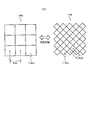
- FIG. 12 is a diagram illustrating a specific configuration of a screen 117 according to another example of the fifth modification. Specifically, FIG. 12 is an enlarged plan view showing a part of the first microlens array unit 117a and the second microlens array unit 117b of the screen 117, which is observed from the direction along the light traveling direction. Is shown. It is assumed that light is incident from the first microlens array unit 117a side.
- the hexagonal apex direction which is the lens contour of the microlens 117aa arranged in the first microlens array portion 117a, and the lens contour of the microlens 117ba arranged in the second microlens array portion 117b.
- the angle difference from the vertex direction of the hexagonal shape is 90 degrees. That is, the first microlens array unit 117a and the second microlens array unit 117b have a plurality of microlenses 117aa and 117ba so that the hexagonal shapes that are the lens contours of the microlenses 117aa and 117ba are rotated by 90 degrees. It is arranged.
- the first micro lens array unit 117a and the second micro lens array unit 117b have a lens pitch Pb3 in the micro lens 117ba of the second micro lens array unit 117b and a lens pitch in the micro lens 117aa of the first micro lens array unit 117a. It is configured to be smaller than Pa3 (for example, “1 ⁇ 2” or less). Further, the first microlens array unit 117a and the second microlens array unit 117b are disposed to face each other at a position separated by at least a distance longer than the focal length of the microlens 117aa of the first microlens array unit 117a.
- the first microlens array unit 117a and the second microlens array unit 117b are arranged as shown in the above-described embodiment and modification examples 1 and 2 (FIG. 3A, FIG. 6, FIG. Any of (see FIG. 8) is applied. Or as shown in the modification 3 (refer FIG. 9), the 1st micro lens array part 117a and the 2nd micro lens array part 117b are comprised integrally.
- the screen 117 according to another example of the modification 5 has the same operation and effect as the screen 11 according to the above-described embodiment and the screen 115 according to the modification 4.
- the hexagonal shape shown in FIGS. 11 and 12 is merely an example, and the present invention is not limited to configuring the lens contour of the microlens in such a hexagonal shape. Further, as shown in FIG. 12, the angle difference in the apex direction of the hexagonal shape that is the lens contour is not limited to 90 degrees.
- the screens according to the above-described Examples and Modifications 1 to 5 are configured by the first and second microlens array units having microlenses whose lens contour is a hexagonal shape (regular hexagonal shape or substantially regular hexagonal shape). It was.
- the screen according to the modification 6 includes first and second microlens array units having microlenses whose lens contours are square.
- FIG. 13 is a diagram illustrating a specific configuration of the screen 118 according to the sixth modification. Specifically, FIG. 13 is an enlarged plan view showing a part of the first microlens array unit 118a and the second microlens array unit 118b of the screen 118, which is observed from the direction along the light traveling direction. Is shown. It is assumed that light is incident from the first microlens array unit 118a side.
- each of the first microlens array unit 118a and the second microlens array unit 118b includes a plurality of microlenses 118aa and 118ba each having a square lens outline in a plan view. It is arranged. Further, in the first microlens array unit 118a and the second microlens array unit 118b, the lens pitch Pb4 in the microlens 118ba of the second microlens array unit 118b is the lens pitch in the microlens 118aa of the first microlens array unit 118a. It is configured to be smaller than Pa4 (for example, “1 ⁇ 2” or less).
- first microlens array unit 118a and the second microlens array unit 118b are disposed to face each other at a position separated by at least a distance longer than the focal length of the microlens 118aa of the first microlens array unit 118a.
- first microlens array unit 118a and the second microlens array unit 118b are arranged as shown in the above-described embodiments and the first and second modifications (FIGS. 3A, 6, 7, and 7). Any of (see FIG. 8) is applied.
- the 1st micro lens array part 118a and the 2nd micro lens array part 118b are comprised integrally.
- the screen 118 according to Modification 6 has the same operation and effect as the screen 11 according to the above-described embodiment.
- the configuration as shown in Modification 4 may be applied to the screen according to Modification 6. That is, the first and second microlens array portions having microlenses configured with square lens contours as shown in FIG. 13 are arranged at the apexes of the lens contours of the microlenses arranged in one microlens array portion. The angle between the direction and the apex direction of the lens contour of the microlens arranged in the other microlens array unit may be shifted.
- FIG. 14 is a diagram illustrating a specific configuration of a screen 119 according to another example of the sixth modification. Specifically, FIG. 14 is an enlarged plan view showing a part of the first microlens array part 119a and the second microlens array part 119b of the screen 119, which is observed from the direction along the light traveling direction. Is shown. It is assumed that light enters from the first microlens array portion 119a side.
- the square apex direction which is the lens outline of the microlens 119aa arranged in the first microlens array part 119a and the lens outline of the microlens 119ba arranged in the second microlens array part 119b.
- the angle difference from the square apex direction is 45 degrees. That is, a plurality of microlenses 119aa and 119ba are provided in the first microlens array portion 119a and the second microlens array portion 119b so that the square shapes which are the lens contours of the microlenses 119aa and 119ba are rotated by 45 degrees. It is arranged.
- the first microlens array unit 119a and the second microlens array unit 119b have a lens pitch Pb5 in the microlens 119ba of the second microlens array unit 119b and a lens pitch in the microlens 119aa of the first microlens array unit 119a. It is configured to be smaller than Pa5 (for example, “1 ⁇ 2” or less). Further, the first microlens array unit 119a and the second microlens array unit 119b are disposed to face each other at a position separated by at least a distance longer than the focal length of the microlens 119aa of the first microlens array unit 119a.
- the first microlens array unit 119a and the second microlens array unit 119b are arranged as shown in the above-described embodiments and the first and second modifications (FIGS. 3A, 6, 7, and 7). Any of (see FIG. 8) is applied. Or as shown in the modification 3 (refer FIG. 9), the 1st micro lens array part 119a and the 2nd micro lens array part 119b are comprised integrally.
- the screen 119 according to another example of the modification 6 has the same functions and effects as the screen 11 according to the above-described embodiment and the screen 115 according to the modification 4.
- the screen according to the modification 7 includes first and second microlens array units having microlenses having a square lens outline. However, the screen according to the modified example 7 is different from the screen according to the modified example 6 in the arrangement of the microlenses having a square shape.
- FIG. 15 is a diagram illustrating a specific configuration of the screen 120 according to the modified example 7. Specifically, FIG. 15 is an enlarged plan view showing a part of the first microlens array unit 120a and the second microlens array unit 120b of the screen 120, which is observed from the direction along the light traveling direction. Is shown. It is assumed that light is incident from the first microlens array unit 120a side.
- each of the first microlens array unit 120a and the second microlens array unit 120b includes a plurality of microlenses 120aa and 120ba each having a square lens outline in plan view. Yes. Specifically, the first microlens array unit 120a and the second microlens array unit 120b are configured such that the microlenses 120aa and 120ba adjacent in the vertical direction are shifted by half the length of one side in the square shape. It is arranged.
- the lens pitch Pb6 in the microlens 120ba of the second microlens array unit 120b is the lens pitch in the microlens 120aa of the first microlens array unit 120a. It is configured to be smaller than Pa6 (for example, “1 ⁇ 2” or less). Furthermore, the first microlens array unit 120a and the second microlens array unit 120b are disposed to face each other at a position separated by at least a distance longer than the focal length of the microlens 120aa of the first microlens array unit 120a.
- the first microlens array unit 120a and the second microlens array unit 120b are arranged as shown in the above-described embodiments and the first and second modifications (FIGS. 3A, 6, 7, and 7). Any of (see FIG. 8) is applied. Or as shown in the modification 3 (refer FIG. 9), the 1st micro lens array part 120a and the 2nd micro lens array part 120b are comprised integrally.
- the screen 120 according to the modified example 7 has the same functions and effects as the screen 11 according to the above-described embodiment.
- the configuration as shown in Modification 4 may be applied to the screen according to Modification 7. That is, the first and second microlens array portions having microlenses configured with a square lens contour as shown in FIG. 15 are arranged at the apexes of the lens contours of the microlenses arranged in one microlens array portion. The angle between the direction and the apex direction of the lens contour of the microlens arranged in the other microlens array unit may be shifted.
- FIG. 16 is a diagram illustrating a specific configuration of a screen 121 according to another example of the modification example 7. Specifically, FIG. 16 is an enlarged plan view showing a part of the first microlens array unit 121a and the second microlens array unit 121b included in the screen 121, as observed from the direction along the light traveling direction. Is shown. It is assumed that light enters from the first microlens array part 121a side.
- a square apex direction which is a lens outline of the microlens 121aa arranged in the first microlens array part 121a and a lens outline of the microlens 121ba arranged in the second microlens array part 121b.
- the angle difference from the square apex direction is 45 degrees. That is, the first microlens array unit 121a and the second microlens array unit 121b have a plurality of microlenses 121aa and 121ba so that the square shapes of the lens contours of the microlenses 121aa and 121ba are rotated by 45 degrees. It is arranged.
- the lens pitch Pb7 in the microlens 121ba of the second microlens array unit 121b is the lens pitch in the microlens 121aa of the first microlens array unit 121a. It is configured to be smaller than Pa7 (for example, “1 ⁇ 2” or less). Furthermore, the first microlens array unit 121a and the second microlens array unit 121b are arranged to face each other at a position separated by at least a distance longer than the focal length of the microlens 121aa of the first microlens array unit 121a.
- the first microlens array part 121a and the second microlens array part 121b are arranged as shown in the above-described embodiments and modifications 1 and 2 (FIG. 3A, FIG. 6, FIG. Any of (see FIG. 8) is applied. Or as shown in the modification 3 (refer FIG. 9), the 1st micro lens array part 121a and the 2nd micro lens array part 121b are comprised integrally.
- the screen 121 according to another example of the modified example 7 has the same functions and effects as the screen 11 according to the above-described embodiment and the screen 115 according to the modified example 4.
- the modification 6 and 7 showed the example which comprises the lens outline of a micro lens in square shape, it is not limited to this, As described in the modification 5, the lens outline of a micro lens is substantially square shape. You may comprise (for example, rectangular shape).
- the screens according to the above-described Examples and Modifications 1 to 7 have first and second microlenses having a lens contour having a regular hexagonal shape (including a substantially regular hexagonal shape) or a square shape (including a substantially square shape). It consisted of a microlens array part.
- the screen according to the modified example 8 includes first and second microlens array units having microlenses having a circular lens outline.
- FIG. 17 is a diagram showing a specific configuration of the screen 122 according to the modified example 7. Specifically, FIG. 17 is an enlarged plan view showing a part of the first microlens array unit 122a and the second microlens array unit 122b of the screen 122, which are observed from a direction along the light traveling direction. Is shown. It is assumed that light enters from the first microlens array portion 122a side.
- each of the first microlens array unit 122a and the second microlens array unit 122b includes a plurality of microlenses 122aa and 122ba each having a circular lens outline in plan view. .
- each of the micro lenses 122aa and 122ba has a plurality of micro lenses 122aa and 122ba arranged at equal intervals.
- the micro lenses 122aa and 122ba are arranged adjacent to each other at predetermined angles around one micro lens.
- FIG. 17 illustrates a case where the predetermined angle is 60 degrees.
- the lens pitch Pb8 in the microlens 122ba of the second microlens array unit 122b is the lens pitch in the microlens 122aa of the first microlens array unit 122a. It is configured to be smaller than Pa8 (for example, “1 ⁇ 2” or less). Further, the first microlens array part 122a and the second microlens array part 122b are arranged to face each other at a position separated by at least a distance longer than the focal length of the microlens 122aa of the first microlens array part 122a.
- the first microlens array part 122a and the second microlens array part 122b are arranged as shown in the above-described embodiments and modifications 1 and 2 (FIG. 3A, FIG. 6, FIG. Any of (see FIG. 8) is applied. Or as shown in the modification 3 (refer FIG. 9), the 1st micro lens array part 122a and the 2nd micro lens array part 122b are comprised integrally.
- the screen 122 according to the modified example 8 has the same operation and effect as the screen 11 according to the above-described embodiment.
- the configuration as shown in Modification 4 may be applied to the screen according to Modification 8. That is, the first and second microlens array units having microlenses configured with circular lens contours as shown in FIG. 17 may be configured to be in a relationship rotated by a predetermined angle.
- FIG. 18 is a diagram illustrating a specific configuration of a screen 123 according to another example of the modification 8. Specifically, FIG. 18 is an enlarged plan view showing a part of the first microlens array portion 123a and the second microlens array portion 123b of the screen 123, which is observed from the direction along the light traveling direction. Is shown. It is assumed that light enters from the first microlens array portion 123a side.
- the microlens 123aa arranged in the first microlens array unit 123a and the microlens 123ba arranged in the second microlens array unit 123b have a predetermined angle with respect to one microlens. It is shifted by 30 degrees corresponding to half.
- the lens pitch Pb9 in the microlens 123ba of the second microlens array unit 123b is the lens pitch in the microlens 123aa of the first microlens array unit 123a. It is configured to be smaller than Pa9 (for example, “1 ⁇ 2” or less).
- first microlens array unit 123a and the second microlens array unit 123b are disposed to face each other at a position separated by at least a distance longer than the focal length of the microlens 123aa of the first microlens array unit 123a.
- the first microlens array part 123a and the second microlens array part 123b are arranged as shown in the above-described embodiments and modifications 1 and 2 (FIG. 3A, FIG. 6, FIG. Any of (see FIG. 8) is applied.
- the 1st micro lens array part 123a and the 2nd micro lens array part 123b are comprised integrally.
- the screen 123 according to another example of the modification 8 has the same operation and effect as the screen 11 according to the above-described embodiment and the screen 115 according to the modification 4.
- the lens contour of the microlens is not limited to being configured in a circular shape, and as described in the fifth modification, the lens contour of the microlens may be configured in a substantially circular shape (for example, an oval shape). Furthermore, as shown in FIG. 18, the first and second microlens array units are not limited to be configured so as to have a relationship of being rotated by 30 degrees.
- Modification 9 Although the example which applies this invention to a head up display was shown above, application of this invention is not limited to this.
- the present invention can be applied to a laser projector other than a head-up display. Since laser projectors usually suffer from speckle noise, it can be said that it is not desirable to use a screen for a liquid crystal projector.
- the screen according to the present invention can appropriately suppress spec noise and sufficiently secure a viewing angle, so that the screen according to the present invention can be suitably applied to a laser projector. it can.
- the present invention can be applied to a head mounted display other than a head-up display and a laser projector.
- the present invention can be used for image display devices such as a head-up display, a head-mounted display, and a laser projector.
Landscapes
- Physics & Mathematics (AREA)
- General Physics & Mathematics (AREA)
- Optics & Photonics (AREA)
- Overhead Projectors And Projection Screens (AREA)
- Lenses (AREA)
- Devices For Indicating Variable Information By Combining Individual Elements (AREA)
Abstract
Description
図1は、本実施例に係る光学素子が適用された画像表示装置の構成を示す。図1に示すように、画像表示装置1は、画像信号入力部2と、ビデオASIC3と、フレームメモリ4と、ROM5と、RAM6と、レーザドライバASIC7と、MEMS制御部8と、レーザ光源ユニット9と、MEMSミラー10と、スクリーン11と、を備える。
次に、本実施例に係るスクリーン11の構成について具体的に説明する。なお、前述したように、スクリーン11は本発明に係る「光学素子」の一例である。
次に、上述した本実施例に係るスクリーン11の作用・効果について説明する。
以下では、上記した実施例の変形例について説明する。なお、上記した実施例と同様の構成については、その説明を適宜省略する。また、特に説明しない構成については、上記した実施例と同様であるものとする。
上記した実施例に係るスクリーン11では、第1マイクロレンズアレイ部11a及び第2マイクロレンズアレイ部11bは、それぞれの対向する面に複数のマイクロレンズ11aa、11baが形成されていた。これに対して、変形例1に係るスクリーンでは、第1及び第2マイクロレンズアレイ部の一方は、対向する面に複数のマイクロレンズが形成され、第1及び第2マイクロレンズアレイ部の他方は、対向する面の反対側の面に複数のマイクロレンズが形成される。言い換えると、変形例1に係るスクリーンでは、第1及び第2マイクロレンズアレイ部において同じ方向を向く面に(具体的には入射光側を向く面または出射光側を向く面に)、複数のマイクロレンズが形成される。
変形例2に係るスクリーンでは、第1及び第2マイクロレンズアレイ部の対向する面の反対側の面に、複数のマイクロレンズがそれぞれ形成される点で、上記した実施例及び変形例1と異なる。
変形例3では、上記した実施例及び変形例1、2のように第1及び第2マイクロレンズアレイ部が別体に構成されておらず、第1及び第2マイクロレンズアレイ部が一体に構成されており、スクリーンの両面に複数のマイクロレンズが形成される。
変形例4に係るスクリーンは、第1及び第2マイクロレンズアレイ部の一方に配列されたマイクロレンズのレンズ輪郭の頂点方向と、第1及び第2マイクロレンズアレイ部の他方に配列されたマイクロレンズのレンズ輪郭の頂点方向との角度をずらせて構成されている点で、上記した実施例及び変形例1乃至3と異なる。
上記した実施例及び変形例1乃至4に係るスクリーンは、レンズ輪郭が、全ての辺の長さが同じである正六角形状であるマイクロレンズを有する第1及び第2マイクロレンズアレイ部にて構成されていた。これに対して、変形例5に係るスクリーンは、レンズ輪郭が正六角形状ではない、略正六角形状(つまり全ての辺の長さが同じではない六角形状)であるマイクロレンズを有する第1及び第2マイクロレンズアレイ部にて構成される。
上記した実施例及び変形例1乃至5に係るスクリーンは、レンズ輪郭が六角形状(正六角形状又は略正六角形状)であるマイクロレンズを有する第1及び第2マイクロレンズアレイ部にて構成されていた。これに対して、変形例6に係るスクリーンは、レンズ輪郭が正方形状であるマイクロレンズを有する第1及び第2マイクロレンズアレイ部にて構成される。
変形例7に係るスクリーンは、変形例6に係るスクリーンと同様に、レンズ輪郭が正方形状であるマイクロレンズを有する第1及び第2マイクロレンズアレイ部にて構成される。しかしながら、変形例7に係るスクリーンは、正方形状であるマイクロレンズの配列が、変形例6に係るスクリーンと異なる。
上記した実施例及び変形例1乃至7に係るスクリーンは、レンズ輪郭が正六角形状(略正六角形状も含む)又は正方形状(略正方形状も含む)であるマイクロレンズを有する第1及び第2マイクロレンズアレイ部にて構成されていた。これに対して、変形例8に係るスクリーンは、レンズ輪郭が円形であるマイクロレンズを有する第1及び第2マイクロレンズアレイ部にて構成される。
上記では本発明をヘッドアップディスプレイに適用する例を示したが、本発明の適用はこれに限定はされない。本発明は、ヘッドアップディスプレイ以外にも、レーザプロジェクタに適用することができる。レーザプロジェクタは通常スペックルノイズが問題となるため、液晶プロジェクタ用のスクリーンを使用することは望ましくないと言える。上記したように、本発明に係るスクリーンは、スペックノイズを適切に抑制することができ、視野角を十分に確保することができるので、本発明に係るスクリーンはレーザプロジェクタに好適に適用することができる。
11 スクリーン
11a 第1マイクロレンズアレイ部
11b 第2マイクロレンズアレイ部
11aa、11ba マイクロレンズ
Claims (18)
- 複数のマイクロレンズが配列された第1マイクロレンズアレイ部及び第2マイクロレンズアレイ部を有する光学素子であって、
前記第1マイクロレンズアレイ部及び前記第2マイクロレンズアレイ部は、
前記第1マイクロレンズアレイ部に配列された前記マイクロレンズの焦点距離よりも長い距離だけ、互いに離間した位置に対向配置され、
前記第2マイクロレンズアレイ部に配列された前記マイクロレンズ同士の間隔が、前記第1マイクロレンズアレイ部に配列された前記マイクロレンズ同士の間隔よりも狭く構成されており、
前記第1マイクロレンズアレイ部は前記第2マイクロレンズアレイ部に対して光の入射側に配置されていることを特徴とする光学素子。 - 前記第1マイクロレンズアレイ部の1のマイクロレンズで集光された光が、前記第2マイクロレンズアレイ部の2以上のマイクロレンズに入射することで分配されるように、前記第1マイクロレンズアレイ部及び前記第2マイクロレンズアレイ部に配列された各マイクロレンズ同士の間隔が設定されていることを特徴とする請求項1に記載の光学素子。
- 前記第2マイクロレンズアレイ部に配列された前記マイクロレンズ同士の間隔が、前記第1マイクロレンズアレイ部に配列された前記マイクロレンズ同士の間隔の「1/2」以下に構成されていることを特徴とする請求項1又は2に記載の光学素子。
- 前記マイクロレンズ同士の間隔は、隣接するマイクロレンズの重心同士の間隔であることを特徴とする請求項1乃至3のいずれか一項に記載の光学素子。
- 前記第1マイクロレンズアレイ部及び前記第2マイクロレンズアレイ部は、前記第1マイクロレンズアレイ部に配列された前記マイクロレンズの焦点距離の1.5倍以上かつ3倍以下の距離だけ離間した位置に対向配置されていることを特徴とする請求項1乃至4のいずれか一項に記載の光学素子。
- 前記複数のマイクロレンズは、それぞれ、平面視において多角形状のレンズ輪郭で構成され、
前記第1マイクロレンズアレイ部及び前記第2マイクロレンズアレイ部は、当該第1マイクロレンズアレイ部に配列された前記マイクロレンズの前記レンズ輪郭の頂点方向と、当該第2マイクロレンズアレイ部に配列された前記マイクロレンズの前記レンズ輪郭の頂点方向との角度をずらせて構成されていることを特徴とする請求項1乃至5のいずれか一項に記載の光学素子。 - 前記多角形状は、正六角形状であり、
前記第1マイクロレンズアレイ部に配列された前記マイクロレンズの前記レンズ輪郭の頂点方向と、前記第2マイクロレンズアレイ部に配列された前記マイクロレンズの前記レンズ輪郭の頂点方向との角度差は、略30度又は略90度であることを特徴とする請求項6に記載の光学素子。 - 前記多角形状は、正方形状であり、
前記第1マイクロレンズアレイ部に配列された前記マイクロレンズの前記レンズ輪郭の頂点方向と、前記第2マイクロレンズアレイ部に配列された前記マイクロレンズの前記レンズ輪郭の頂点方向との角度差は、略45度又は略135度であることを特徴とする請求項6に記載の光学素子。 - 前記複数のマイクロレンズは、それぞれ、平面視において正多角形状のレンズ輪郭を有し、
前記第1マイクロレンズアレイ部及び前記第2マイクロレンズアレイ部は、当該第1マイクロレンズアレイ部に配列された前記マイクロレンズの前記レンズ輪郭の頂点方向と、当該第2マイクロレンズアレイ部に配列された前記マイクロレンズの前記レンズ輪郭の頂点方向との角度を、前記正多角形状に含まれる1の内角の半分の角度ずらせて構成されていることを特徴とする請求項1乃至5のいずれか一項に記載の光学素子。 - 前記第1マイクロレンズアレイ部及び前記第2マイクロレンズアレイ部は、それぞれ前記複数のマイクロレンズが等間隔に配列され、
前記マイクロレンズは、1のマイクロレンズ周囲に、前記1のマイクロレンズの頂点に対してそれぞれ所定角度ごとに隣接して配列され、
前記第1マイクロレンズアレイ部に配列された前記マイクロレンズと、前記第2マイクロレンズアレイ部に配列された前記マイクロレンズとが、前記1のマイクロレンズに対して前記所定角度の半分の角度ずらせて構成されていることを特徴とする請求項1乃至5のいずれか一項に記載の光学素子。 - 前記第1マイクロレンズアレイ部及び前記第2マイクロレンズアレイ部を構成するマイクロレンズの間を光が透過しないようにマスクしたことを特徴とする請求項10に記載の光学素子。
- 前記第1マイクロレンズアレイ部を一方の面に有する第1レンズアレイと、前記第2マイクロレンズアレイ部を一方の面に有する第2レンズアレイとから構成されることを特徴とする請求項1乃至11のいずれか一項に記載の光学素子。
- 前記第1マイクロレンズアレイ部及び前記第2マイクロレンズアレイ部は、前記第1レンズアレイ及び前記第2レンズアレイの、各々対向する面に形成されていることを特徴とする請求項12に記載の光学素子。
- 前記第1マイクロレンズアレイ部は、前記第1レンズアレイの面のうち、前記第2レンズアレイの前記第2マイクロレンズアレイ部が形成されている面と対向しない面に形成されていることを特徴とする請求項12に記載の光学素子。
- 前記第1マイクロレンズアレイ部及び前記第2マイクロレンズアレイ部は、前記第1レンズアレイ及び前記第2レンズアレイの、各々対向しない面に形成されていることを特徴とする請求項12に記載の光学素子。
- 前記第1マイクロレンズアレイ部を一方の面に有し、前記第2マイクロレンズアレイ部を他方の面に有することを特徴とする請求項1乃至11のいずれか一項に記載の光学素子。
- 請求項1乃至16のいずれか一項に記載の光学素子を備え、前記光学素子によって形成された画像をユーザの目の位置から虚像として視認させることを特徴とするヘッドアップディスプレイ。
- 光源と、
複数のマイクロレンズが所定の間隔で配列された第1マイクロレンズアレイと、
前記所定の間隔よりも狭い間隔で複数のマイクロレンズが配列された第2マイクロレンズアレイと、
を有し、
前記第2マイクロレンズアレイは、前記第1マイクロレンズアレイに配置されたマクロレンズの焦点距離よりも長い距離だけ離間した位置に配置され、
前記第1マイクロレンズアレイは、前記第2マイクロレンズアレイに対して、前記光源から出射される光の入射側に配置されていることを特徴とする光源ユニット。
Priority Applications (3)
| Application Number | Priority Date | Filing Date | Title |
|---|---|---|---|
| PCT/JP2011/059281 WO2012140765A1 (ja) | 2011-04-14 | 2011-04-14 | 光学素子、ヘッドアップディスプレイ及び光源ユニット |
| JP2011552652A JP5021850B1 (ja) | 2011-04-14 | 2011-04-14 | 光源ユニット及びヘッドアップディスプレイ |
| US14/111,987 US9042021B2 (en) | 2011-04-14 | 2011-04-14 | Optical element, head-up display and light source unit |
Applications Claiming Priority (1)
| Application Number | Priority Date | Filing Date | Title |
|---|---|---|---|
| PCT/JP2011/059281 WO2012140765A1 (ja) | 2011-04-14 | 2011-04-14 | 光学素子、ヘッドアップディスプレイ及び光源ユニット |
Publications (1)
| Publication Number | Publication Date |
|---|---|
| WO2012140765A1 true WO2012140765A1 (ja) | 2012-10-18 |
Family
ID=46980516
Family Applications (1)
| Application Number | Title | Priority Date | Filing Date |
|---|---|---|---|
| PCT/JP2011/059281 Ceased WO2012140765A1 (ja) | 2011-04-14 | 2011-04-14 | 光学素子、ヘッドアップディスプレイ及び光源ユニット |
Country Status (3)
| Country | Link |
|---|---|
| US (1) | US9042021B2 (ja) |
| JP (1) | JP5021850B1 (ja) |
| WO (1) | WO2012140765A1 (ja) |
Cited By (8)
| Publication number | Priority date | Publication date | Assignee | Title |
|---|---|---|---|---|
| JP2013064985A (ja) * | 2011-08-29 | 2013-04-11 | Denso Corp | ヘッドアップディスプレイ装置 |
| JP2014095815A (ja) * | 2012-11-09 | 2014-05-22 | Funai Electric Co Ltd | プロジェクタおよび投影用スクリーン |
| WO2015097759A1 (ja) * | 2013-12-24 | 2015-07-02 | パイオニア株式会社 | 光学素子及び画像表示装置 |
| JP2015169816A (ja) * | 2014-03-07 | 2015-09-28 | 船井電機株式会社 | 光学部品の結露防止構造、及び、ヘッドアップディスプレイ装置 |
| JP2016038400A (ja) * | 2014-08-05 | 2016-03-22 | 株式会社日立エルジーデータストレージ | 映像投射装置及びこれを用いたヘッドマウントディスプレイ |
| JP2016045385A (ja) * | 2014-08-25 | 2016-04-04 | 大日本印刷株式会社 | 透過型スクリーン及びそれを用いたヘッドアップディスプレイ装置 |
| JP2017122923A (ja) * | 2017-02-27 | 2017-07-13 | 船井電機株式会社 | プロジェクタおよびスクリーン |
| CN110892308A (zh) * | 2017-05-12 | 2020-03-17 | 真三维公司 | 近眼中央凹显示器 |
Families Citing this family (6)
| Publication number | Priority date | Publication date | Assignee | Title |
|---|---|---|---|---|
| US9736895B1 (en) * | 2013-10-03 | 2017-08-15 | Ketra, Inc. | Color mixing optics for LED illumination device |
| KR102413740B1 (ko) | 2014-10-31 | 2022-06-29 | 현대모비스 주식회사 | 차량용 헤드 업 디스플레이 장치 |
| JP6504353B2 (ja) * | 2015-04-28 | 2019-04-24 | 株式会社リコー | 画像表示装置及び物体装置 |
| US9983337B2 (en) | 2015-08-07 | 2018-05-29 | Samsung Electronics Co., Ltd. | Light emitting diode display apparatus |
| KR102266749B1 (ko) * | 2015-08-07 | 2021-06-24 | 삼성전자주식회사 | 엘이디 디스플레이장치 |
| CN116840948B (zh) * | 2022-11-26 | 2024-05-17 | 荣耀终端有限公司 | 一种光学透镜、光体积描记器和电子设备 |
Citations (6)
| Publication number | Priority date | Publication date | Assignee | Title |
|---|---|---|---|---|
| JPH11183867A (ja) * | 1997-12-17 | 1999-07-09 | Semiconductor Energy Lab Co Ltd | 液晶プロジェクタ |
| JPH11271669A (ja) * | 1998-03-20 | 1999-10-08 | Matsushita Electric Ind Co Ltd | 照明手段と当該手段を用いた照明光学装置及び投写型表示装置 |
| JP2000241769A (ja) * | 1999-02-23 | 2000-09-08 | Seiko Epson Corp | 照明光学系および投写型表示装置 |
| JP2001352429A (ja) * | 2000-04-05 | 2001-12-21 | Rohm Co Ltd | レンズアレイユニットおよびこれを備えた光学装置 |
| JP2005338325A (ja) * | 2004-05-26 | 2005-12-08 | Nippon Seiki Co Ltd | 表示装置 |
| JP2010277065A (ja) * | 2009-04-28 | 2010-12-09 | Nippon Seiki Co Ltd | ヘッドアップディスプレイ装置 |
Family Cites Families (15)
| Publication number | Priority date | Publication date | Assignee | Title |
|---|---|---|---|---|
| JPH0727995A (ja) * | 1993-07-14 | 1995-01-31 | Mitsubishi Rayon Co Ltd | 結像素子 |
| US5513123A (en) | 1994-06-30 | 1996-04-30 | Nec Usa, Inc. | Non-scan design-for-testability of RT-level data paths |
| JP2864103B2 (ja) * | 1995-03-01 | 1999-03-03 | 日本ビクター株式会社 | 投射型カラー表示装置 |
| US6678023B1 (en) | 1997-12-17 | 2004-01-13 | Semiconductor Energy Laboratory Co., Ltd. | Liquid crystal projector |
| JP4182374B2 (ja) * | 1998-10-29 | 2008-11-19 | ソニー株式会社 | 投射型表示装置 |
| US6707613B2 (en) | 2000-04-05 | 2004-03-16 | Rohm Co., Ltd. | Lens array unit and method of forming image |
| US6643067B2 (en) * | 2000-11-22 | 2003-11-04 | Seiko Epson Corporation | Electro-optical device and electronic apparatus |
| JP2002373503A (ja) * | 2001-06-15 | 2002-12-26 | Matsushita Electric Ind Co Ltd | 照明装置及び投写型表示装置 |
| JP4268399B2 (ja) * | 2002-11-01 | 2009-05-27 | パイオニア株式会社 | 画像表示装置 |
| US7106519B2 (en) * | 2003-07-31 | 2006-09-12 | Lucent Technologies Inc. | Tunable micro-lens arrays |
| AU2004294182C1 (en) * | 2003-11-21 | 2014-01-16 | Visual Physics, Llc | Micro-optic security and image presentation system |
| WO2005078511A1 (en) | 2004-02-04 | 2005-08-25 | Microvision, Inc. | Scanned-beam heads-up display and related systems and methods |
| WO2006072260A1 (de) * | 2005-01-04 | 2006-07-13 | Hentze-Lissotschenko Patentverwaltungs Gmbh & Co. Kg | Strahlteileranordnung |
| JP2010145745A (ja) | 2008-12-18 | 2010-07-01 | Equos Research Co Ltd | 画像形成装置、及び、ヘッドアップディスプレイ装置 |
| JP2010225307A (ja) * | 2009-03-19 | 2010-10-07 | Tohoku Univ | 偏光機能付光源とホモジェナイザーとこれらを用いた光源装置とこれを用いたローカルディミングバックライトシステム |
-
2011
- 2011-04-14 JP JP2011552652A patent/JP5021850B1/ja not_active Expired - Fee Related
- 2011-04-14 WO PCT/JP2011/059281 patent/WO2012140765A1/ja not_active Ceased
- 2011-04-14 US US14/111,987 patent/US9042021B2/en not_active Expired - Fee Related
Patent Citations (6)
| Publication number | Priority date | Publication date | Assignee | Title |
|---|---|---|---|---|
| JPH11183867A (ja) * | 1997-12-17 | 1999-07-09 | Semiconductor Energy Lab Co Ltd | 液晶プロジェクタ |
| JPH11271669A (ja) * | 1998-03-20 | 1999-10-08 | Matsushita Electric Ind Co Ltd | 照明手段と当該手段を用いた照明光学装置及び投写型表示装置 |
| JP2000241769A (ja) * | 1999-02-23 | 2000-09-08 | Seiko Epson Corp | 照明光学系および投写型表示装置 |
| JP2001352429A (ja) * | 2000-04-05 | 2001-12-21 | Rohm Co Ltd | レンズアレイユニットおよびこれを備えた光学装置 |
| JP2005338325A (ja) * | 2004-05-26 | 2005-12-08 | Nippon Seiki Co Ltd | 表示装置 |
| JP2010277065A (ja) * | 2009-04-28 | 2010-12-09 | Nippon Seiki Co Ltd | ヘッドアップディスプレイ装置 |
Cited By (10)
| Publication number | Priority date | Publication date | Assignee | Title |
|---|---|---|---|---|
| JP2013064985A (ja) * | 2011-08-29 | 2013-04-11 | Denso Corp | ヘッドアップディスプレイ装置 |
| JP2014095815A (ja) * | 2012-11-09 | 2014-05-22 | Funai Electric Co Ltd | プロジェクタおよび投影用スクリーン |
| US9658465B2 (en) | 2012-11-09 | 2017-05-23 | Funai Electric Co., Ltd. | Projector and screen |
| WO2015097759A1 (ja) * | 2013-12-24 | 2015-07-02 | パイオニア株式会社 | 光学素子及び画像表示装置 |
| JP2015169816A (ja) * | 2014-03-07 | 2015-09-28 | 船井電機株式会社 | 光学部品の結露防止構造、及び、ヘッドアップディスプレイ装置 |
| JP2016038400A (ja) * | 2014-08-05 | 2016-03-22 | 株式会社日立エルジーデータストレージ | 映像投射装置及びこれを用いたヘッドマウントディスプレイ |
| US10466490B2 (en) | 2014-08-05 | 2019-11-05 | Hitachi-Lg Data Storage, Inc. | Video projection device and head mounted display using the same |
| JP2016045385A (ja) * | 2014-08-25 | 2016-04-04 | 大日本印刷株式会社 | 透過型スクリーン及びそれを用いたヘッドアップディスプレイ装置 |
| JP2017122923A (ja) * | 2017-02-27 | 2017-07-13 | 船井電機株式会社 | プロジェクタおよびスクリーン |
| CN110892308A (zh) * | 2017-05-12 | 2020-03-17 | 真三维公司 | 近眼中央凹显示器 |
Also Published As
| Publication number | Publication date |
|---|---|
| JP5021850B1 (ja) | 2012-09-12 |
| US20140055864A1 (en) | 2014-02-27 |
| US9042021B2 (en) | 2015-05-26 |
| JPWO2012140765A1 (ja) | 2014-07-28 |
Similar Documents
| Publication | Publication Date | Title |
|---|---|---|
| JP5112556B2 (ja) | 光源ユニット及びヘッドアップディスプレイ | |
| JP5021850B1 (ja) | 光源ユニット及びヘッドアップディスプレイ | |
| JP4769912B1 (ja) | 光学素子、ヘッドアップディスプレイ及び光学素子の製造方法 | |
| JP5149446B2 (ja) | 光源ユニット及びヘッドアップディスプレイ | |
| JP4954346B1 (ja) | ヘッドアップディスプレイ | |
| JP5048154B1 (ja) | 画像表示装置 | |
| JP6696236B2 (ja) | 表示装置および導光装置 | |
| JP5321520B2 (ja) | 直視型の画像表示装置 | |
| CN107407813B (zh) | 图像显示装置 | |
| JP6387800B2 (ja) | 光束径拡大素子および表示装置 | |
| CN107148589A (zh) | 平视显示装置 | |
| WO2016139769A1 (ja) | レンズアレイ及び映像投影装置 | |
| JPWO2013153655A1 (ja) | 光学素子、ヘッドアップディスプレイ及び光源ユニット | |
| JP2012226301A (ja) | 光源ユニット及びヘッドアップディスプレイ | |
| JP2016188901A (ja) | 表示装置 | |
| JP5837685B2 (ja) | 光源ユニット及びヘッドアップディスプレイ | |
| JP2012226302A (ja) | 光源ユニット及びヘッドアップディスプレイ | |
| JP2015225216A (ja) | 画像表示装置 | |
| JP2012083456A (ja) | 虚像表示装置 | |
| US20170045739A1 (en) | Transmission-type screen and headup display | |
| US20190011697A1 (en) | Transmission-type screen and head-up display | |
| WO2015097759A1 (ja) | 光学素子及び画像表示装置 |
Legal Events
| Date | Code | Title | Description |
|---|---|---|---|
| ENP | Entry into the national phase |
Ref document number: 2011552652 Country of ref document: JP Kind code of ref document: A |
|
| 121 | Ep: the epo has been informed by wipo that ep was designated in this application |
Ref document number: 11863565 Country of ref document: EP Kind code of ref document: A1 |
|
| NENP | Non-entry into the national phase |
Ref country code: DE |
|
| WWE | Wipo information: entry into national phase |
Ref document number: 14111987 Country of ref document: US |
|
| 122 | Ep: pct application non-entry in european phase |
Ref document number: 11863565 Country of ref document: EP Kind code of ref document: A1 |