WO2012132386A1 - 検出方法および検出装置 - Google Patents
検出方法および検出装置 Download PDFInfo
- Publication number
- WO2012132386A1 WO2012132386A1 PCT/JP2012/002073 JP2012002073W WO2012132386A1 WO 2012132386 A1 WO2012132386 A1 WO 2012132386A1 JP 2012002073 W JP2012002073 W JP 2012002073W WO 2012132386 A1 WO2012132386 A1 WO 2012132386A1
- Authority
- WO
- WIPO (PCT)
- Prior art keywords
- light
- amount
- detected
- sensor
- substance
- Prior art date
- Legal status (The legal status is an assumption and is not a legal conclusion. Google has not performed a legal analysis and makes no representation as to the accuracy of the status listed.)
- Ceased
Links
Images





Classifications
-
- G—PHYSICS
- G01—MEASURING; TESTING
- G01N—INVESTIGATING OR ANALYSING MATERIALS BY DETERMINING THEIR CHEMICAL OR PHYSICAL PROPERTIES
- G01N21/00—Investigating or analysing materials by the use of optical means, i.e. using sub-millimetre waves, infrared, visible or ultraviolet light
- G01N21/62—Systems in which the material investigated is excited whereby it emits light or causes a change in wavelength of the incident light
- G01N21/63—Systems in which the material investigated is excited whereby it emits light or causes a change in wavelength of the incident light optically excited
- G01N21/64—Fluorescence; Phosphorescence
- G01N21/645—Specially adapted constructive features of fluorimeters
- G01N21/648—Specially adapted constructive features of fluorimeters using evanescent coupling or surface plasmon coupling for the excitation of fluorescence
Definitions
- the present invention relates to a detection method and a detection apparatus for optically measuring the amount of a substance to be detected in a sample solution.
- a fluorescence detection method has been widely used as a highly sensitive and easy measurement method in biomeasurement and the like.
- the presence of the detection target substance is detected by irradiating the sample, which is considered to contain a detection target substance that emits fluorescence when excited with light of a specific wavelength, with the excitation light of the specific wavelength. It is a method to confirm.
- the detection target substance is not a fluorescent substance, this binding, that is, by detecting the fluorescence in the same manner as described above by contacting the sample with a substance that is labeled with a fluorescent dye and specifically binds to the detection target substance. The existence of a detection target substance is also widely confirmed.
- Patent Document 1 a method using a surface plasmon enhancement effect is proposed in Patent Document 1 and the like. This is because the surface plasmon resonance is generated, so that the sensor part provided with the metal film in a predetermined region on the transparent support is opposite to the metal layer forming surface of the support with respect to the interface between the support and the metal film.
- S / N is obtained by making excitation light incident at a predetermined angle equal to or greater than the total reflection angle from the surface side of the substrate, generating surface plasmons on the metal layer by irradiation of the excitation light, and enhancing fluorescence by the electric field enhancement action. Is to improve.
- the surface plasmon enhancement depends on the intensity and incident angle of the excitation light on the metal film.
- the surface plasmon enhancement shows a steep characteristic with respect to the incident angle of the excitation light on the metal film.
- the plasmon enhancement varies greatly, and as a result, the detected fluorescence intensity varies. That is, if there are variations in the installation accuracy of the sensor chip, the surface accuracy of the sensor portion of the sensor chip, and the incident angle accuracy of the excitation light, there is a problem that the measurement result is not stable and the measurement accuracy is lowered.
- Patent Document 2 proposes an apparatus capable of absorbing an angle error within a convergence angle by using convergent light having a plurality of angle components for excitation light. .
- the light emitted from the light source has a light intensity that changes depending on the position of the light beam (for example, the distance from the light beam center derived from the angle of divergence from the light source) (that is, there is an intensity distribution).
- an optical system such as a diaphragm is further combined with the light at the center of the light beam.
- a device has also been devised to suppress variation in the intensity of the excitation light for each incident angle by using only a region having a high intensity.
- Patent Document 2 can deal with errors caused by fluctuations in the incident angle of the excitation light with respect to the metal film, but only a small amount of light near the center of the light beam is emitted from the light source. As a result, the intensity of the excitation light is lowered as a whole and the detection sensitivity is lowered.
- the present invention has been made in view of the above problems, and in a detection method and a detection apparatus for optically measuring the amount of a substance to be detected in a sample liquid using a surface plasmon enhancement effect, excitation light for a metal film It is an object of the present invention to provide a detection method and a detection apparatus that have a small error due to fluctuations in the incident angle and a high detection sensitivity.
- the detection method of the present invention includes a sensor unit formed by laminating a metal film on one surface of a dielectric plate, and the sensor unit is divided into a plurality of plane regions having different inclination angles with respect to a predetermined reference plane.
- the sample liquid containing the substance to be detected is brought into contact with the sensor part of the sensor chip, whereby an amount of the fluorescent label binding substance corresponding to the quantity of the substance to be detected contained in the sample liquid is placed on the sensor part.
- the sensor chip is irradiated with excitation light sequentially for each plane area of the sensor chip, and the amount of light generated in the sensor unit in response to the excitation light irradiation is detected for each plane area of the sensor chip.
- the amount of the substance to be detected is measured based on the detection result of the planar region in which the most amount of light is detected.
- the sensor chip when the sensor chip includes a microchannel through which the sample liquid is circulated, and a plurality of sensor units having the same planar area configuration are provided in the microchannel, a plurality of sensors are provided.
- the amount of light is detected in each plane area of the reference sensor unit, and the amount of light is the largest among the plurality of plane areas of the reference sensor unit.
- the detected plane area is determined, and for the remaining sensor sections of the plurality of sensor sections, the amount of light is only in the plane area corresponding to the plane area where the most amount of light is detected in the reference sensor section. It is preferable to perform detection.
- the detection device of the present invention is a detection device used in the above-described detection method, and selectively irradiates excitation light for each planar area of a housing portion that houses a sensor chip and a sensor chip that is housed in the housing portion. Based on the excitation light irradiation optical system, the light detection means for detecting the amount of light generated in the sensor unit in response to the excitation light irradiation, and the amount of the detected substance based on the amount of light detected by the light detection means And measuring means for measuring.
- the sensor unit includes a sensor unit formed by laminating a metal film on one surface of the dielectric plate, and the sensor unit is provided in a plurality of plane regions having different inclination angles with respect to a predetermined reference plane.
- the sample liquid containing the substance to be detected is brought into contact with the sensor part of the sensor chip, whereby an amount of fluorescent label binding corresponding to the quantity of the substance to be detected contained in the sample liquid A substance is bonded onto the sensor unit, and excitation light is sequentially irradiated to each planar region of the sensor chip, and the amount of light generated in the sensor unit is detected for each planar region of the sensor chip in response to irradiation of the excitation light.
- the amount of the substance to be detected is measured based on the detection result of the planar area in which the largest amount of light is detected among the plurality of planar areas.
- a sensor chip that includes a sensor unit formed by laminating a metal film on one surface of a dielectric plate and is divided into a plurality of plane regions having different inclination angles with respect to a predetermined reference plane is used, parallel light Even when is used as excitation light, angle adjustment within the setting range of the inclination angle of the plurality of planar regions can be made unnecessary.
- the excitation light is irradiated sequentially for each planar area of the sensor chip, all the excitation light emitted from the light source can be irradiated for each planar area, so that the excitation light intensity at the time of detection can be increased. Can be high.
- the sensor chip when the sensor chip includes a micro flow channel through which the sample liquid is circulated and a plurality of sensor units having the same planar area configuration are provided in the micro flow channel, any one of the plurality of sensor units is provided.
- the amount of light is detected for each plane region of the reference sensor unit, and the plane region in which the most amount of light is detected among the plurality of plane regions of the reference sensor unit
- the amount of light is detected only in the plane region corresponding to the plane region where the most amount of light is detected in the reference sensor unit. By doing so, the total number of detections can be reduced, so that efficient measurement can be performed.
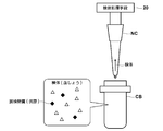
- FIG. 2 is a schematic diagram showing how a sample is extracted from a sample container using a nozzle tip by the sample processing means of FIG.
- FIG. 2 is a schematic diagram showing how the sample in the nozzle tip is injected and stirred into the reagent cell by the sample processing means of FIG.
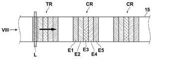
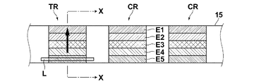
- Top view showing the configuration of the sensor portion of the sensor chip Sectional drawing for each planar area of the sensor section viewed from the direction of arrow VIII in FIG. The top view which shows the other structure of the sensor part of the said sensor chip XX sectional view in FIG.
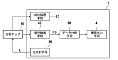
- FIG. 1 is a schematic diagram of a fluorescence detection device according to an embodiment of the present invention
- FIG. 2 is a block diagram of the fluorescence detection device
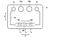
- FIG. 3 is a schematic diagram illustrating an example of a sensor chip used in the fluorescence detection device
- FIG. 5 is a schematic diagram showing how a sample is extracted from a sample container using a nozzle tip by the sample processing means in FIG. 2
- FIG. 5 is a diagram in which the sample in the nozzle chip is injected and stirred into the reagent cell by the sample processing means
- FIG. 6 is a schematic diagram showing an example of the light irradiation means and the fluorescence detection means of FIG. 2
- FIG. 7 is a top view showing the configuration of the sensor portion of the sensor chip
- FIG. 8 is a diagram in FIG. It is sectional drawing for every plane area
- This fluorescence detection device 1 is an immunological analysis device using surface plasmon resonance, and when performing analysis by the fluorescence detection device 1, a sample container CB containing the sample shown in FIG. 1 and a sample and a reagent are extracted. The nozzle chip NC used at the time, and the sensor chip 10 formed with the reagent cell and the micro flow path are loaded. The sample container CB, the nozzle tip NC, and the sensor chip 10 are all disposable items that are discarded once they are used. Then, the fluorescence detection apparatus 1 performs quantitative or qualitative analysis on the test substance in the sample while flowing the sample through the micro flow path 15 of the sensor chip 10.
- the fluorescence detection apparatus 1 includes a sample processing means 20, a light irradiation means 30, a fluorescence detection means 40, a data analysis means 50, and the like.
- the sample processing means 20 extracts a sample from the sample container CB containing the sample using the nozzle chip NC, and generates a sample solution obtained by mixing and stirring the extracted sample with a reagent.
- FIG. 3 is a schematic diagram showing an example of the sensor chip 10.
- the sensor chip 10 has a structure in which an inlet 12, an outlet 13, sample cells 14 a and 14 b, and a flow path 15 are formed in a main body 11 made of a dielectric plate such as a light transmissive resin.
- the injection port 12 communicates with the discharge port 13 via the flow channel 15, and by applying a negative pressure from the discharge port 13, the specimen is injected from the injection port 12, flows into the flow channel 15, and is discharged from the discharge port 13.
- the sample cells 14a and 14b are containers for storing a fluorescent reagent (second antibody) to be mixed with the specimen in the specimen container CB. Note that the openings of the sample cells 14a and 14b are sealed with a sealing member, and the sealing member is pierced when the specimen and the fluorescent reagent are mixed.
- test region TR as a measurement sensor unit for detecting a test substance in the specimen is formed in the flow path 15, and in the test region TR, downstream of the test region TR.
- a control region CR is formed as a correction sensor unit for acquiring information for correcting the measurement result.
- the first antibody is immobilized on the test region TR, and the labeled antibody is captured by a so-called sandwich method.
- a reference antibody is fixed to the control region CR, and the reference antibody captures the fluorescent substance when the sample solution flows on the control region CR.
- Two control regions CR are formed, and in order from the upstream side, a so-called negative control region CR for detecting non-specific adsorption and a so-called positive type for detecting a difference in reactivity due to a difference in specimen.
- the control region CR is formed.
- the test area TR and the two control areas CR are divided into five plane areas E1 to E5 in the traveling direction of the flow path 15, as shown in FIGS.
- the five plane regions E1 to E5 have different inclination angles with respect to the horizontal direction (reference plane), and the plane region E1 is inclined by ⁇ 2 ° with respect to the horizontal direction in the direction orthogonal to the traveling direction of the flow path 15.
- E2 is inclined by -1 ° in the direction orthogonal to the traveling direction of the flow path 15 with respect to the horizontal direction
- the plane area E3 is parallel to the horizontal direction
- the plane area E4 is parallel to the horizontal direction.
- the plane region E5 is inclined 2 ° in the direction orthogonal to the traveling direction of the flow path 15 with respect to the horizontal direction.
- the configuration of the planar areas E1 to E5 of the test area TR and the two control areas CR is the same.
- the sample processing means 20 Aspirates the sample from the sample container CB using the nozzle tip NC as shown in FIG. Thereafter, the sample processing means 20 punctures the seal member of the sample cell 14a as shown in FIG. 5, mixes and stirs the sample with the reagent in the sample cell 14a, and then sucks the sample solution again using the nozzle tip NC. . This operation is similarly performed for the sample cell 14b. Then, a sample solution is generated in which the second antibody B2, which is a second binding substance specifically binding in the reagent, to the test substance (antigen) A present in the sample is modified on the surface. Then, the sample processing means 20 installs the nozzle chip NC containing the sample solution on the injection port 12, and the sample solution in the nozzle chip NC flows into the flow path 15 by the negative pressure from the discharge port 13.
- the sample processing unit 20 supplies the sample solution in which the sample and the reagent are mixed into the flow path 15
- the reagent is filled in the flow path 15 in advance, and the sample processing means 20 Only the specimen may be allowed to flow from the inlet 12.
- FIG. 6 is a schematic diagram showing an example of the light irradiation means 30 and the fluorescence detection means 40.
- the light irradiating means 30 in FIG. 2 selects the excitation light L, which is parallel light from the back side of the sensor chip 10, at one of the plane areas E1 to E5 of the test area TR through the prism at an incident angle that is a total reflection condition. Is intended to be irradiated.
- the fluorescence detection means 40 is composed of, for example, a CCD, a CMOS, or the like, and detects the amount of fluorescence Lf generated in the test area TR or the control area CR.
- the excitation light L is incident on the interface between the dielectric plate 17 and the metal film 16 at a specific incident angle equal to or greater than the total reflection angle by the light irradiation means 30, thereby entering the sample S on the metal film 16.
- the evanescent wave Ew oozes out, and surface plasmons are excited in the metal film 16 by the evanescent wave Ew.
- This surface plasmon causes an electric field distribution on the surface of the metal film 16 to form an electric field enhancement region.
- the fluorescent labeling substance F bound to the first antibody B1 fixed on the metal film 16 is excited by the evanescent wave Ew to generate enhanced fluorescence Lf.
- metal quenching may occur and the sensitivity may be lowered.
- a quenching prevention layer made of a silica layer, a polystyrene layer, or the like is provided on the metal layer 16, Such a problem can be solved.
- the fluorescent labeling substance F for example, as a quenching preventive substance such as a fluorescent dye encapsulated in polystyrene particles or silica particles, or a gold colloid surface coated with polystyrene, the problem of metal quenching is solved. be able to.
- the data analysis means 50 in FIG. 2 analyzes the test substance based on the signal FS based on the light quantity of the fluorescence Lf detected by the fluorescence detection means 40.
- the irradiation position of the excitation light L is moved along the traveling direction of the flow path 15 for each of the planar regions E1 to E5 in the positive control region CR.
- the excitation light L is sequentially irradiated as described above, and the amount of light generated at that time is detected. Then, among the plane areas E1 to E5, the plane area with the highest detected light amount is specified. Then, the measurement result in the control region CR is acquired based on the detection result of the planar region having the highest detected light amount.
- test region TR and the negative control region CR were irradiated with the excitation light L only in the same planar region as the planar region having the highest detected light amount in the detection in the positive control region CR, and occurred at that time. Detect the amount of light. For example, when the detected light amount in the plane area E2 is the highest in the positive type control area CR, the test area TR and the negative type control area CR are irradiated with the excitation light L only in the plane area E2 and generated at that time. Detect the amount of light.
- the analysis result obtained as described above is output from the information output means 4 composed of a monitor, a printer or the like.
- the excitation light L can be parallel light
- the optical system can have a simple configuration without requiring a special optical system as described in Patent Document 2 above, so that the cost can be reduced. Can be kept low.
- the test region TR and the two control regions CR may be divided into five planar regions E1 to E5 in a direction orthogonal to the traveling direction of the flow path 15, as shown in FIGS.
- the five plane regions E1 to E5 have different inclination angles with respect to the horizontal direction (reference plane), and the plane region E1 is inclined by ⁇ 2 ° with respect to the horizontal direction in a direction orthogonal to the traveling direction of the flow path 15.
- the plane region E2 is inclined by -1 ° in the direction perpendicular to the traveling direction of the flow path 15 with respect to the horizontal direction, the plane region E3 is parallel to the horizontal direction, and the plane region E4 is parallel to the horizontal direction.
- the plane region E5 is inclined by 2 ° in the direction orthogonal to the traveling direction of the flow path 15 with respect to the horizontal direction.
- the configuration of the planar areas E1 to E5 of the test area TR and the two control areas CR is the same.
- each of the planar regions E1 to E5 is sequentially irradiated with the excitation light L by moving the irradiation position of the excitation light L along the direction orthogonal to the traveling direction of the flow path 15. The amount of light generated at that time is detected.
- the number of division into each planar region is not limited to five, and a plurality of other numbers may be used. Further, the division mode may be divided in a two-dimensional manner instead of a one-dimensional manner as described above. Further, the inclination angle of each planar region is not limited to the above.
Landscapes
- Health & Medical Sciences (AREA)
- Nuclear Medicine, Radiotherapy & Molecular Imaging (AREA)
- Physics & Mathematics (AREA)
- Life Sciences & Earth Sciences (AREA)
- Chemical & Material Sciences (AREA)
- Analytical Chemistry (AREA)
- Biochemistry (AREA)
- General Health & Medical Sciences (AREA)
- General Physics & Mathematics (AREA)
- Immunology (AREA)
- Pathology (AREA)
- Investigating, Analyzing Materials By Fluorescence Or Luminescence (AREA)
Abstract
【課題】 表面プラズモン増強効果を利用して、試料液中の被検出物質の量を光学的に測定する検出方法および検出装置において、金属膜に対する励起光の入射角の変動に起因する誤差を少なくするとともに、検出感度も高くする。 【解決手段】 誘電体プレート(17)の一面上に金属膜(16)が積層されて形成されたセンサ部を備え、センサ部が所定の基準平面に対する傾斜角度の異なる5つの平面領域(E1~E5)に分割されてなるセンサチップを用いて、センサチップのセンサ部上に、被検出物質を含む試料液を接触させることにより、試料液に含有される被検出物質の量に応じた量の蛍光標識結合物質をセンサ部上に結合させ、センサチップの各平面領域(E1~E5)毎に順次励起光を照射し、センサチップの各平面領域(E1~E5)毎に励起光の照射に応じてセンサ部で発生した光の量を検出し、平面領域(E1~E5)の中で最も光の量が多く検出された平面領域の検出結果に基づいて、被検出物質の量を測定する。
Description
本発明は、試料液中の被検出物質の量を光学的に測定する検出方法および検出装置に関するものである。
従来、バイオ測定等において、高感度かつ容易な測定法として蛍光検出法が広く用いられている。この蛍光検出法は、特定波長の光により励起されて蛍光を発する検出対象物質を含むと考えられる試料に上記特定波長の励起光を照射し、そのとき蛍光を検出することによって検出対象物質の存在を確認する方法である。また、検出対象物質が蛍光体ではない場合、蛍光色素で標識されて検出対象物質と特異的に結合する物質を試料に接触させ、その後上記と同様にして蛍光を検出することにより、この結合すなわち検出対象物質の存在を確認することも広くなされている。
また、このような蛍光検出法において、感度を向上させるため、表面プラズモン増強効果を利用する方法が特許文献1などに提案されている。これは、表面プラズモン共鳴を生じさせるため、透明な支持体上の所定領域に金属膜を設けたセンサ部に対し、支持体と金属膜との界面に対して支持体の金属層形成面と反対の面側から、全反射角以上の所定の角度で励起光を入射させ、この励起光の照射により金属層に表面プラズモンを生じさせ、その電場増強作用によって、蛍光を増強させることによりS/Nを向上させるものである。
また、上記に示した蛍光法のように蛍光標識からの蛍光を検出するのではなく、その蛍光が金属層に新たに表面プラズモンを誘起することによって生じる放射光(SPCE: Surface Plasmon-Coupled Emission)を検出する方法も提案されている。
表面プラズモン増強度は金属膜に対する励起光の強度や入射角等に依存し、中でも金属膜に対する励起光の入射角に対しては急峻な特性を示すため、入射角が僅かに変動しただけで表面プラズモン増強度が大きく変動して、その結果、検出される蛍光の強度が変動することになる。すなわち、センサチップの設置精度や、センサチップのセンサ部の面精度や、励起光の入射角精度にバラツキがあると、測定結果が安定せずに測定精度が低下するという問題がある。
このような問題を解消するため、特許文献2では、励起光について複数の角度成分を持つ収束光を用いることにより、収束角度内での角度誤差を吸収することが可能な装置が提案されている。通常、光源から射出される光は、光束の位置(例えば、光源からの発散角の角度に由来する光束中心からの距離)によって光の強度が変化する(つまり、強度分布がある)ため、表面プラズモン共鳴が発生する角度が変化することで、表面プラズモンによる電場増強作用の度合いが変化してしまうという問題があるため、特許文献2では、さらに絞り等の光学系を組み合わせて、光束中心の光強度が高い領域のみを使用するようにして、入射角毎の励起光の強度のバラツキを抑える工夫もなされている。
しかしながら、特許文献2に記載の手段では、金属膜に対する励起光の入射角の変動に起因する誤差については対処できるものの、光源から出射された光のうち光束中心付近の僅かな光のみしか励起光として用いないため、今度は励起光の強度が全体的に下がってしまい、検出感度が低下するという問題があった。
本発明は上記問題に鑑みてなされたものであり、表面プラズモン増強効果を利用して、試料液中の被検出物質の量を光学的に測定する検出方法および検出装置において、金属膜に対する励起光の入射角の変動に起因する誤差が少なく、また検出感度も高い検出方法および検出装置を提供することを目的とする。
本発明の検出方法は、誘電体プレートの一面上に金属膜が積層されて形成されたセンサ部を備え、センサ部が所定の基準平面に対する傾斜角度の異なる複数の平面領域に分割されてなるセンサチップを用いて、センサチップのセンサ部上に、被検出物質を含む試料液を接触させることにより、試料液に含有される被検出物質の量に応じた量の蛍光標識結合物質をセンサ部上に結合させ、センサチップの各平面領域毎に順次励起光を照射し、センサチップの各平面領域毎に励起光の照射に応じてセンサ部で発生した光の量を検出し、複数の平面領域の中で最も光の量が多く検出された平面領域の検出結果に基づいて、被検出物質の量を測定することを特徴とするものである。
本発明の検出方法においては、センサチップが、試料液を流通させる微小流路を備え、微小流路内に平面領域の構成が同じセンサ部が複数設けられたものである場合に、複数のセンサ部のうちのいずれか一つのセンサ部を基準センサ部として、基準センサ部の各平面領域毎に前記光の量を検出し、基準センサ部の複数の平面領域の中で最も光の量が多く検出された平面領域を決定し、複数のセンサ部のうちの残りのセンサ部については、基準センサ部において最も光の量が多く検出された平面領域と対応する平面領域についてのみ、前記光の量の検出を行うようにすることが好ましい。
本発明の検出装置は、上記検出方法に用いられる検出装置であって、センサチップを収容する収容部と、収容部に収容されたセンサチップの各平面領域毎に選択的に励起光を照射する励起光照射光学系と、励起光の照射に応じてセンサ部で発生した光の量を検出する光検出手段と、光検出手段により検出された光の量に基づいて、被検出物質の量を測定する測定手段とを備えてなることを特徴とするものである。
本発明の検出方法および検出装置によれば、誘電体プレートの一面上に金属膜が積層されて形成されたセンサ部を備え、センサ部が所定の基準平面に対する傾斜角度の異なる複数の平面領域に分割されてなるセンサチップを用いて、センサチップのセンサ部上に、被検出物質を含む試料液を接触させることにより、試料液に含有される被検出物質の量に応じた量の蛍光標識結合物質をセンサ部上に結合させ、センサチップの各平面領域毎に順次励起光を照射し、センサチップの各平面領域毎に励起光の照射に応じてセンサ部で発生した光の量を検出し、複数の平面領域の中で最も光の量が多く検出された平面領域の検出結果に基づいて、被検出物質の量を測定するようにしている。
誘電体プレートの一面上に金属膜が積層されて形成されたセンサ部を備え、センサ部が所定の基準平面に対する傾斜角度の異なる複数の平面領域に分割されてなるセンサチップを用いれば、平行光を励起光として用いた場合でも、複数の平面領域の傾斜角度の設定範囲内での角度調整を不要とすることができる。
また、センサチップの各平面領域毎に順次励起光を照射するようにしているため、各平面領域毎に光源から出射された励起光を全て照射することができるため、検出時の励起光強度を高くすることができる。
従って、金属膜に対する励起光の入射角の変動に起因する誤差を少なくすることができるとともに、検出感度も高くすることができる。
また、センサチップが、試料液を流通させる微小流路を備え、微小流路内に平面領域の構成が同じセンサ部が複数設けられたものである場合に、複数のセンサ部のうちのいずれか一つのセンサ部を基準センサ部として、基準センサ部の各平面領域毎に前記光の量を検出し、基準センサ部の複数の平面領域の中で最も光の量が多く検出された平面領域を決定し、複数のセンサ部のうちの残りのセンサ部については、基準センサ部において最も光の量が多く検出された平面領域と対応する平面領域についてのみ、前記光の量の検出を行うようにすれば、全体の検出回数を少なくすることができるため、効率的な測定を行うことが可能となる。
以下、図面を参照して本発明の一実施の形態について詳細に説明する。図1は本発明の一実施の形態の蛍光検出装置の模式図、図2は上記蛍光検出装置のブロック図、図3は上記蛍光検出装置に用いられるセンサチップの一例を示す模式図、図4は図2の検体処理手段によりノズルチップを用いて検体が検体容器から抽出される様子を示す模式図、図5は図2の検体処理手段によりノズルチップ内の検体が試薬セルに注入・撹拌される様子を示す模式図、図6は図2の光照射手段および蛍光検出手段の一例を示す模式図、図7は上記センサチップのセンサ部の構成を示す上面図、図8は図7中のVIII矢指方向から見たセンサ部の各平面領域毎の断面図である。
この蛍光検出装置1は、表面プラズモン共鳴を利用した免疫解析装置であって、蛍光検出装置1により分析を行う際、図1に示す検体が収容された検体容器CBと、検体および試薬を抽出する際に用いられるノズルチップNCと、試薬セルおよびマイクロ流路が形成されたセンサチップ10が装填される。なお、検体容器CB、ノズルチップNCおよびセンサチップ10はいずれも一度使用したら破棄される使い捨てのものである。そして、蛍光検出装置1は検体をセンサチップ10のマイクロ流路15に流しながら検体内の被検物質について定量的もしくは定性的な分析を行う。
この蛍光検出装置1は、検体処理手段20、光照射手段30、蛍光検出手段40、データ分析手段50等を備えている。検体処理手段20は、ノズルチップNCを用いて検体を収容した検体容器CB内から検体を抽出し、抽出した検体を試薬と混合撹拌した検体溶液を生成するものである。
ここで、図3はセンサチップ10の一例を示す模式図である。センサチップ10は、光透過性の樹脂等の誘電体プレートからなる本体11に注入口12、排出口13、試料セル14a、14b、流路15が形成された構造を有している。注入口12は流路15を介して排出口13に連通しており、排出口13から負圧をかけることにより検体は注入口12から注入されて流路15内に流れ排出口13から排出される。試料セル14a、14bは検体容器CB内の検体に混合する蛍光試薬(第2抗体)を収容する容器である。なお、試料セル14a、14bの開口部はシール部材により封止されており、検体と蛍光試薬とを混合する際にシール部材が穿孔されるようになっている。
また、流路15内には、検体内の被検物質を検出するための測定用のセンサ部としてのテスト領域TRが形成されており、このテスト領域TRの下流側には、テスト領域TRにおける測定結果を補正するための情報を取得するための補正用のセンサ部としてのコントロール領域CRが形成されている。
テスト領域TR上には第1抗体が固定されており、いわゆるサンドイッチ方式により標識化された抗体を捕捉する。また、コントロール領域CRには参照抗体が固定されており、コントロール領域CR上に検体溶液が流れることにより参照抗体が蛍光物質を捕捉する。なお、コントロール領域CRは2つ形成されており、上流側から順に、非特異吸着を検出するためのいわゆるネガ型のコントロール領域CRと、検体差による反応性の違いを検出するためのいわゆるポジ型のコントロール領域CRとが形成されている。
テスト領域TRおよび2つのコントロール領域CRは、図7、8に示すように、流路15の進行方向において5つの平面領域E1~E5に分割されている。5つの平面領域E1~E5は水平方向(基準平面)に対する傾斜角度が全て異なり、平面領域E1は水平方向に対して流路15の進行方向と直交する方向において-2°傾いており、平面領域E2は水平方向に対して流路15の進行方向と直交する方向において-1°傾いており、平面領域E3は水平方向に対して平行であり、平面領域E4は水平方向に対して流路15の進行方向と直交する方向において1°傾いており、平面領域E5は水平方向に対して流路15の進行方向と直交する方向において2°傾いている。なお、テスト領域TRおよび2つのコントロール領域CRの各々の平面領域E1~E5の構成は同一である。
分析の開始が指示された際、検体処理手段20は図4に示すようにノズルチップNCを用いて検体容器CBから検体を吸引する。その後、検体処理手段20は図5に示すように試料セル14aのシール部材を穿孔し試料セル14a内の試薬に検体を混合・撹拌させた後、検体溶液を再びノズルチップNCを用いて吸引する。この動作を試料セル14bについても同様に行う。すると、検体内に存在する被検物質(抗原)Aに試薬内の特異的に結合する第2の結合物質である第2抗体B2が表面に修飾された検体溶液が生成される。そして、検体処理手段20は、検体溶液を収容したノズルチップNCを注入口12上に設置し、排出口13からの負圧によりノズルチップNC内の検体溶液が流路15内に流入する。
なお、検体処理手段20が検体と試薬とを混合した検体溶液を流路15内に供給する場合について例示しているが、流路15内に予め試薬を充填させておき、検体処理手段20が注入口12から検体のみを流入させるようにしてもよい。
図6は光照射手段30および蛍光検出手段40の一例を示す模式図である。なお、図6においてはテスト領域TRに着目して説明するが、コントロール領域CRについても同様に励起光Lが照射されるものである。図2の光照射手段30は、センサチップ10の裏面側から平行光とした励起光Lを全反射条件となる入射角度でプリズムを介してテスト領域TRの平面領域E1~E5のいずれかに選択的に照射するものである。蛍光検出手段40は、たとえばCCD、CMOS等からなり、テスト領域TRもしくはコントロール領域CRにおいて発生した蛍光Lfの光量を検出するものである。
そして、光照射手段30により励起光Lが誘電体プレート17と金属膜16との界面に対して全反射角以上の特定の入射角度で入射されることにより、金属膜16上の試料S中にエバネッセント波Ewが滲み出し、このエバネッセント波Ewによって金属膜16中に表面プラズモンが励起される。この表面プラズモンにより金属膜16表面に電界分布が生じ、電場増強領域が形成される。すると、金属膜16上に固着された第1抗体B1と結合した蛍光標識物質Fはエバネッセント波Ewにより励起され増強された蛍光Lfを発生する。
なお、プラズモン増強を利用した検出においては、金属消光が発生して感度が低下するおそれがあるため、例えばシリカ層やポリスチレン層等からなる消光防止層を金属層16上に設けるようにすれば、このような問題を解消することができる。また、蛍光標識物質Fについて、例えば、蛍光色素をポリスチレン粒子やシリカ粒子に内包したものや、金コロイド表面をポリスチレンでコーティングしたもの等といった、消光防止性物質としても、金属消光の問題を解消することができる。
図2のデータ分析手段50は、蛍光検出手段40により検出された蛍光Lfの光量に基づいた信号FSに基づいて、被検物質の分析を行うものである。
ここで、本実施の形態における分析時の処理について詳細に説明する。
本実施の形態では、まずポジ型のコントロール領域CRにおける平面領域E1~E5の各々について、図7に示すように、流路15の進行方向に沿って励起光Lの照射位置を移動させて、上記のように励起光Lを順次照射し、その際に発生した光の量を検出する。そして平面領域E1~E5の中で、最も検出光量が高い平面領域を特定する。そして、最も検出光量が高い平面領域の検出結果に基づいて、コントロール領域CRにおける測定結果を取得する。
また、テスト領域TRおよびネガ型のコントロール領域CRについては、ポジ型のコントロール領域CRでの検出において最も検出光量が高い平面領域と同じ平面領域についてのみ励起光Lを照射し、その際に発生した光の量を検出する。例えば、ポジ型のコントロール領域CRにおいて平面領域E2の検出光量が最も高かった場合には、テスト領域TRおよびネガ型のコントロール領域CRについては平面領域E2のみ励起光Lを照射し、その際に発生した光の量を検出する。
上記のようにして得られた分析結果は、モニタやプリンタ等からなる情報出力手段4から出力される。
このような態様とすることにより、平行光を励起光Lとして用いた場合でも、平面領域E1~E5の傾斜角度の範囲内での角度誤差を吸収することができる。また、平面領域E1~E5毎に順次励起光Lを照射するようにしているため、各平面領域E1~E5毎に光源から出射された励起光Lを全て照射することができるため、検出時の励起光Lの強度を高くすることができる。従って、金属膜16に対する励起光の入射角の変動に起因する誤差を少なくすることができるとともに、検出感度も高くすることができる。また、励起光Lは平行光とすることができるので、光学系については上記特許文献2に記載されているような特別な光学系を必要とせずに簡素な構成とすることができるので、コストを低く抑えることができる。
以上、本発明の好ましい実施の形態について説明したが、本発明は上記実施の形態に限定されるものではない。
例えば、テスト領域TRおよび2つのコントロール領域CRは、図9、10に示すように、流路15の進行方向と直交する方向において5つの平面領域E1~E5に分割してもよい。ここで、5つの平面領域E1~E5は水平方向(基準平面)に対する傾斜角度が全て異なり、平面領域E1は水平方向に対して流路15の進行方向と直交する方向において-2°傾いており、平面領域E2は水平方向に対して流路15の進行方向と直交する方向において-1°傾いており、平面領域E3は水平方向に対して平行であり、平面領域E4は水平方向に対して流路15の進行方向と直交する方向において1°傾いており、平面領域E5は水平方向に対して流路15の進行方向と直交する方向において2°傾いている。なお、テスト領域TRおよび2つのコントロール領域CRの各々の平面領域E1~E5の構成は同一である。この場合、平面領域E1~E5の各々について、図10に示すように、流路15の進行方向と直交する方向に沿って励起光Lの照射位置を移動させて励起光Lを順次照射し、その際に発生した光の量を検出する。
また、センサ部の構成について、各平面領域に分割する数は5つに限らず、それ以外の複数の数としてもよい。また、分割の態様についても上記のように一次元状に分割するのではなく、二次元状に分割してもよい。また、各平面領域の傾斜角度についても上記に限定されるものではない。
さらに、上記以外にも、本発明の要旨を逸脱しない範囲において、各種の改良や変形を行なってもよいのは勿論である。
Claims (3)
- 誘電体プレートの一面上に金属膜が積層されて形成されたセンサ部を備え、該センサ部が所定の基準平面に対する傾斜角度の異なる複数の平面領域に分割されてなるセンサチップを用いて、
該センサチップの前記センサ部上に、被検出物質を含む試料液を接触させることにより、該試料液に含有される被検出物質の量に応じた量の蛍光標識結合物質を前記センサ部上に結合させ、
前記センサチップの各平面領域毎に順次励起光を照射し、
前記センサチップの各平面領域毎に前記励起光の照射に応じて前記センサ部で発生した光の量を検出し、
複数の平面領域の中で最も光の量が多く検出された平面領域の検出結果に基づいて、前記被検出物質の量を測定することを特徴とする検出方法。 - 前記センサチップが、前記試料液を流通させる微小流路を備え、該微小流路内に平面領域の構成が同じセンサ部が複数設けられたものである場合に、
前記複数のセンサ部のうちのいずれか一つのセンサ部を基準センサ部として、該基準センサ部の各平面領域毎に前記光の量を検出し、
前記基準センサ部の複数の平面領域の中で最も光の量が多く検出された平面領域を決定し、
前記複数のセンサ部のうちの残りのセンサ部については、前記基準センサ部において最も光の量が多く検出された平面領域と対応する平面領域についてのみ、前記光の量の検出を行うことを特徴とする請求項1記載の検出方法。 - 請求項1または2記載の検出方法に用いられる検出装置であって、
前記センサチップを収容する収容部と、
該収容部に収容された前記センサチップの各平面領域毎に選択的に励起光を照射する励起光照射光学系と、
前記励起光の照射に応じて前記センサ部で発生した光の量を検出する光検出手段と、
該光検出手段により検出された光の量に基づいて、前記被検出物質の量を測定する測定手段とを備えてなることを特徴とする検出装置。
Applications Claiming Priority (2)
| Application Number | Priority Date | Filing Date | Title |
|---|---|---|---|
| JP2011-081303 | 2011-03-31 | ||
| JP2011081303A JP5669312B2 (ja) | 2011-03-31 | 2011-03-31 | 検出方法および検出装置 |
Publications (1)
| Publication Number | Publication Date |
|---|---|
| WO2012132386A1 true WO2012132386A1 (ja) | 2012-10-04 |
Family
ID=46930162
Family Applications (1)
| Application Number | Title | Priority Date | Filing Date |
|---|---|---|---|
| PCT/JP2012/002073 Ceased WO2012132386A1 (ja) | 2011-03-31 | 2012-03-26 | 検出方法および検出装置 |
Country Status (2)
| Country | Link |
|---|---|
| JP (1) | JP5669312B2 (ja) |
| WO (1) | WO2012132386A1 (ja) |
Citations (4)
| Publication number | Priority date | Publication date | Assignee | Title |
|---|---|---|---|---|
| JPH09292332A (ja) * | 1996-04-25 | 1997-11-11 | Fuji Photo Film Co Ltd | 表面プラズモンセンサー |
| JP2003121349A (ja) * | 2001-08-07 | 2003-04-23 | Mitsubishi Chemicals Corp | 表面プラズモン共鳴センサチップ、並びにそれを用いた試料の分析方法及び分析装置 |
| JP2009204484A (ja) * | 2008-02-28 | 2009-09-10 | Fujifilm Corp | センシング装置 |
| JP2010203900A (ja) * | 2009-03-03 | 2010-09-16 | Konica Minolta Holdings Inc | 表面プラズモン増強蛍光センサおよび表面プラズモン増強蛍光センサに用いられるチップ構造体 |
Family Cites Families (2)
| Publication number | Priority date | Publication date | Assignee | Title |
|---|---|---|---|---|
| JPWO2010134470A1 (ja) * | 2009-05-20 | 2012-11-12 | コニカミノルタホールディングス株式会社 | 表面プラズモン増強蛍光測定装置および表面プラズモン増強蛍光測定装置に用いられるプラズモン励起センサ |
| JP5488351B2 (ja) * | 2010-09-02 | 2014-05-14 | コニカミノルタ株式会社 | 表面プラズモン励起増強蛍光測定装置およびこれに用いられるセンサ構造体 |
-
2011
- 2011-03-31 JP JP2011081303A patent/JP5669312B2/ja not_active Expired - Fee Related
-
2012
- 2012-03-26 WO PCT/JP2012/002073 patent/WO2012132386A1/ja not_active Ceased
Patent Citations (4)
| Publication number | Priority date | Publication date | Assignee | Title |
|---|---|---|---|---|
| JPH09292332A (ja) * | 1996-04-25 | 1997-11-11 | Fuji Photo Film Co Ltd | 表面プラズモンセンサー |
| JP2003121349A (ja) * | 2001-08-07 | 2003-04-23 | Mitsubishi Chemicals Corp | 表面プラズモン共鳴センサチップ、並びにそれを用いた試料の分析方法及び分析装置 |
| JP2009204484A (ja) * | 2008-02-28 | 2009-09-10 | Fujifilm Corp | センシング装置 |
| JP2010203900A (ja) * | 2009-03-03 | 2010-09-16 | Konica Minolta Holdings Inc | 表面プラズモン増強蛍光センサおよび表面プラズモン増強蛍光センサに用いられるチップ構造体 |
Also Published As
| Publication number | Publication date |
|---|---|
| JP5669312B2 (ja) | 2015-02-12 |
| JP2012215478A (ja) | 2012-11-08 |
Similar Documents
| Publication | Publication Date | Title |
|---|---|---|
| JP5666277B2 (ja) | 分析チップ | |
| KR101884091B1 (ko) | 사다리꼴 입사구조 프리즘 입사형 실리콘 기반 액침 미세유로 측정장치 및 측정방법 | |
| RU2519505C2 (ru) | Сенсорное устройство для определения целевого вещества | |
| US20090218496A1 (en) | Sensing apparatus and a method of detecting substances | |
| US8178046B2 (en) | Microfluidic devices with SPR sensing capabilities | |
| JP2007501403A (ja) | 白色光反射干渉の分光変化規則に基づく光ファイバアレイバイオチップ | |
| JP2005257455A (ja) | 測定装置および測定ユニット | |
| US20090221089A1 (en) | Probe chip, sensing apparatus using the same and method of detecting substances using the same | |
| JP2014119418A (ja) | 測定装置および測定方法 | |
| JP2012202742A (ja) | 検出方法および検出装置 | |
| JP2006064514A (ja) | 測定ユニット | |
| US10895535B2 (en) | Measurement method, and measuring chip and measuring kit used for the same | |
| JP5797427B2 (ja) | 検出方法および検出装置 | |
| JP5487150B2 (ja) | 光学的測定方法および光学的測定装置 | |
| EP3413056B1 (en) | Liquid delivery method, and detection system using said method | |
| JP2004219401A (ja) | 表面プラズモンセンサー及び、表面プラズモン共鳴測定装置、検知チップ | |
| JP5669312B2 (ja) | 検出方法および検出装置 | |
| JP2015111063A (ja) | 表面プラズモン増強蛍光測定方法および表面プラズモン増強蛍光測定装置 | |
| JP2013113690A (ja) | 分析素子、分析装置、および分析方法 | |
| JP5681077B2 (ja) | 測定方法および測定装置 | |
| JP2012202911A (ja) | 分析チップ | |
| JP3945636B2 (ja) | 測定装置 | |
| JP6768621B2 (ja) | 表面プラズモン共鳴を利用した蛍光検出装置及びその作動方法 | |
| JP2013076673A (ja) | 測定装置 | |
| JP6481371B2 (ja) | 検出方法および検出キット |
Legal Events
| Date | Code | Title | Description |
|---|---|---|---|
| 121 | Ep: the epo has been informed by wipo that ep was designated in this application |
Ref document number: 12764972 Country of ref document: EP Kind code of ref document: A1 |
|
| NENP | Non-entry into the national phase |
Ref country code: DE |
|
| 122 | Ep: pct application non-entry in european phase |
Ref document number: 12764972 Country of ref document: EP Kind code of ref document: A1 |