WO2012128329A1 - 中間転写ベルトの製造方法 - Google Patents
中間転写ベルトの製造方法 Download PDFInfo
- Publication number
- WO2012128329A1 WO2012128329A1 PCT/JP2012/057383 JP2012057383W WO2012128329A1 WO 2012128329 A1 WO2012128329 A1 WO 2012128329A1 JP 2012057383 W JP2012057383 W JP 2012057383W WO 2012128329 A1 WO2012128329 A1 WO 2012128329A1
- Authority
- WO
- WIPO (PCT)
- Prior art keywords
- layer
- intermediate transfer
- transfer belt
- gas
- inorganic compound
- Prior art date
- Legal status (The legal status is an assumption and is not a legal conclusion. Google has not performed a legal analysis and makes no representation as to the accuracy of the status listed.)
- Ceased
Links
Images



Classifications
-
- G—PHYSICS
- G03—PHOTOGRAPHY; CINEMATOGRAPHY; ANALOGOUS TECHNIQUES USING WAVES OTHER THAN OPTICAL WAVES; ELECTROGRAPHY; HOLOGRAPHY
- G03G—ELECTROGRAPHY; ELECTROPHOTOGRAPHY; MAGNETOGRAPHY
- G03G15/00—Apparatus for electrographic processes using a charge pattern
- G03G15/14—Apparatus for electrographic processes using a charge pattern for transferring a pattern to a second base
- G03G15/16—Apparatus for electrographic processes using a charge pattern for transferring a pattern to a second base of a toner pattern, e.g. a powder pattern, e.g. magnetic transfer
- G03G15/1605—Apparatus for electrographic processes using a charge pattern for transferring a pattern to a second base of a toner pattern, e.g. a powder pattern, e.g. magnetic transfer using at least one intermediate support
- G03G15/162—Apparatus for electrographic processes using a charge pattern for transferring a pattern to a second base of a toner pattern, e.g. a powder pattern, e.g. magnetic transfer using at least one intermediate support details of the the intermediate support, e.g. chemical composition
Definitions
- the present invention relates to a method for producing an intermediate transfer belt used in an electrophotographic image forming apparatus such as an electrophotographic copying machine or a printer.
- seamless belt members are used for various functions and applications in the apparatus.
- a fixing belt, a transfer belt, a paper conveying belt, and the like can be given.
- An electrophotographic image forming apparatus supplies charged toner to an electrostatic latent image on a photoconductor in contact or non-contact manner, and transfers a toner image formed through a developing process to make the electrostatic latent image a visible image Then, after primary transfer to an intermediate transfer member, which is a transfer member, secondary transfer is performed on a transfer material (for example, paper), and further fixed by a fixing member to form a final image.
- an intermediate transfer member which is a transfer member
- secondary transfer is performed on a transfer material (for example, paper), and further fixed by a fixing member to form a final image.
- a four-color toner image formed on a photosensitive member is temporarily transferred (primary transfer) to an intermediate transfer member, whereby a full-color image is formed on the intermediate transfer member.
- An intermediate transfer body system in which a film is formed and then transferred onto a transfer medium (recording medium) such as paper at once (secondary transfer) is becoming mainstream.
- a transfer medium such as paper at once
- secondary transfer As the intermediate transfer member, an intermediate transfer belt using an endless belt member and an intermediate transfer roll using a tubular member are used.
- the intermediate transfer member faces the intermediate transfer member in order to obtain high speed.
- a system called a tandem system in which color developing devices for respective colors are arranged in series is the mainstream, and an intermediate transfer belt is often used from the viewpoint of the mechanism.
- Primary transferability when the toner image on the photoconductor is primarily transferred to the intermediate transfer belt as a subject of the intermediate transfer belt method that is tubular in response to the demand for high image quality full color and high quality
- secondary transferability when the toner image on the intermediate transfer belt is secondarily transferred to a recording medium may be mentioned.
- the transferability includes primary transferability and secondary transferability.
- the intermediate transfer belt system has the following problems. 1. As the toner remaining on the intermediate transfer belt is removed or contacted in the secondary transfer to the transfer medium (recording medium), the surface of the intermediate transfer belt is damaged and streaky image unevenness occurs. 2. If there is residual toner remaining on the intermediate transfer belt, an abnormal image such as uneven color or fog occurs. Moreover, it becomes a factor of deterioration of durability due to filming. 3. As the toner remaining on the intermediate transfer belt is removed, the surface of the intermediate transfer belt is scratched and toner removal residue is likely to occur, which affects the life of the intermediate transfer belt.
- An intermediate transfer belt has been studied for the purpose of exhibiting a transfer rate and transfer performance and preventing the occurrence of abnormal images such as voids, density unevenness, and color unevenness.
- adjustment of the thickness of the elastic layer effective for high-quality transfer efficiency provided on the substrate adjustment of the thickness of the surface layer made of a resin layer containing diamond fine particles effective for wear resistance, It is known to obtain an intermediate transfer belt satisfying high image quality transfer efficiency and wear resistance by performing adjustment or the like (see, for example, Patent Document 1).
- the intermediate transfer belt described in Patent Document 1 has a life that achieves both transfer efficiency and wear resistance, and has an elastic layer thickness and diamond fine particle content.
- the n-dodecane contact angle effective for improving the releasability with the oil (wax component) contained in the toner on the base layer is set to 20 ° or more, and a pencil hardness of 4H or more effective for preventing scratches on the surface of the layer. It is known to obtain an intermediate transfer belt that provides high image quality transfer efficiency by providing a coat layer (see, for example, Patent Document 2).
- the present invention has been made in view of the above circumstances, and the object thereof is to form a high-quality image without causing a decrease in transfer efficiency, scratch resistance, and filming resistance even after long-term printing.
- An object of the present invention is to provide an intermediate transfer belt manufacturing method that can be used.
- the surface layer should not contain particulate substances (diamond particles, inorganic particles, organic particles, etc.) that cause defects such as cracks, scratches, foreign matter adhesion, and filming. 2) In order not to generate cracks, scratches, and surface layer scraping, and to prevent cracks from being generated by bending (stretching direction, shrinking direction) load, a high-hardness surface layer should be formed thinly. 3) The surface layer should be smooth in order to suppress adhesion of paper dust and foreign matters.
- the transfer efficiency may change or image quality unevenness may occur if the environmental humidity for printing changes. Therefore, there is a possibility that high-quality transfer efficiency cannot be maintained during a long-term printing process.
- the present inventors have found that hydrophilic groups remain in the thin film having an inorganic compound. As can be seen, in order to reduce the remaining hydrophilic groups, it is necessary to increase the cross-linking density of the thin film having the inorganic compound. By performing the irradiation with vacuum ultraviolet light on the thin film having the inorganic compound, As soon as the present invention has been found, it is possible to form an intermediate transfer belt in which the transfer efficiency does not change even when the crosslinking density increases and the environmental humidity for printing changes.
- FIG. 1 is a schematic cross-sectional configuration diagram illustrating an example of an electrophotographic image forming apparatus that uses an intermediate transfer belt as an intermediate transfer member.
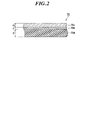
- FIG. 2 is an enlarged schematic cross-sectional view of the intermediate transfer belt shown in FIG. 1. It is the schematic of the atmospheric pressure plasma processing apparatus which forms the thin film which has the inorganic compound which forms the surface layer of an intermediate transfer belt. It is the schematic of the other atmospheric pressure plasma processing apparatus which forms the thin film which has the inorganic compound which forms the surface layer of an intermediate transfer belt.
- FIG. 4 is an enlarged schematic view of a portion indicated by P in FIG. 3. It is the schematic of the modifier of the thin film which has the inorganic compound which forms a surface layer.
- FIG. 1 is a schematic sectional view showing an example of an electrophotographic image forming apparatus using an intermediate transfer belt as an intermediate transfer member. This figure shows the case of a full-color image forming apparatus.
- the full-color image forming apparatus 1 includes a plurality of sets of image forming units 10Y, 10M, 10C, and 10K, an endless belt-shaped intermediate transfer body forming unit 7 as a transfer unit, and an endless belt-shaped paper feeding conveyance for conveying a recording medium P. And a belt type fixing device 24 as fixing means.
- a document image reading device SC is arranged on the upper part of the main body A of the full-color image forming apparatus 1.
- An image forming unit 10Y that forms a yellow image as one of different color toner images formed on each of the photoreceptors 1Y, 1M, 1C, and 1K is a drum-like photoreceptor as a first image carrier. 1Y, a charging unit 2Y arranged around the photoreceptor 1Y, an exposure unit 3Y, a developing unit 4Y having a developer carrier 4Y1, a primary transfer roller 5Y as a primary transfer unit, and a cleaning unit 6Y.
- An image forming unit 10M that forms a magenta image as another different color toner image is disposed around a drum-shaped photoconductor 1M as a first image carrier, and the photoconductor 1M.
- an image forming unit 10C for forming a cyan image as one of different toner images of different colors is disposed around a drum-shaped photoreceptor 1C as a first image carrier, and the photoreceptor 1C.
- the charging means 2C, the exposure means 3C, the developing means 4C having the developer carrier 4C1, the primary transfer roller 5C as the primary transfer means, and the cleaning means 6C are provided.
- an image forming unit 10K that forms a black image as one of other different color toner images is disposed around a drum-shaped photosensitive member 1K as a first image carrier, and the photosensitive member 1K. It has a charging means 2K, an exposure means 3K, a developing means 4K having a developer carrier 4K1, a primary transfer roller 5K as a primary transfer means, and a cleaning means 6K.
- the endless belt-shaped intermediate transfer body forming unit 7 has an endless intermediate transfer belt 70 as a second image carrier having a semiconductive endless belt shape that is wound around a plurality of rollers and is rotatably supported.
- Each color image formed by the image forming units 10Y, 10M, 10C, and 10K is sequentially transferred and synthesized on the rotating endless intermediate transfer belt 70 by the primary transfer rollers 5Y, 5M, 5C, and 5K.
- a color image is formed.
- a recording medium P such as paper as a recording medium accommodated in the paper feeding cassette 20 is fed by the paper feeding / conveying means 21, passes through a plurality of intermediate rollers 22 A, 22 B, 22 C, 22 D, and a registration roller 23, and is secondary.
- a color image is transferred onto the recording medium P at a time by being conveyed to a secondary transfer roller 5A as a transfer means.
- the recording medium P onto which the color image has been transferred is fixed by the fixing device 24 to which the heat roller fixing device 270 is attached, and is sandwiched between the discharge rollers 25 and placed on the discharge tray 26 outside the apparatus.
- the residual toner is removed by the cleaning means 6A from the endless intermediate transfer belt 70 which has separated the curvature of the recording medium P.
- the primary transfer roller 5K is always in pressure contact with the photoreceptor 1K.
- the other primary transfer rollers 5Y, 5M, and 5C are in pressure contact with the corresponding photoreceptors 1Y, 1M, and 1C, respectively, only during color image formation.
- the secondary transfer roller 5A is pressed against the endless intermediate transfer belt 70 only when the recording medium P passes through the secondary transfer roller 5A.
- the housing 8 includes image forming units 10Y, 10M, 10C, and 10K, and an endless belt-shaped intermediate transfer body forming unit 7.
- the image forming units 10Y, 10M, 10C, and 10K are arranged in tandem in the vertical direction.
- An endless belt-shaped intermediate transfer body forming unit 7 is disposed on the left side of the photoreceptors 1Y, 1M, 1C, and 1K in the figure.
- the endless belt-shaped intermediate transfer body forming unit 7 includes an endless intermediate transfer belt 70 that can be rotated by winding rollers 71, 72, 73, 74, and 76, primary transfer rollers 5Y, 5M, 5C, and 5K, and a cleaning unit 6A. And have.
- the image forming units 10Y, 10M, 10C, and 10K and the endless belt-shaped intermediate transfer body forming unit 7 are integrally pulled out from the main body A by the drawer operation of the housing 8.
- the outer peripheral surfaces of the photoreceptors 1Y, 1M, 1C, and 1K are charged and exposed to form a latent image on the outer peripheral surface, and then a toner image (developed image) is formed by development.
- the toner images of the respective colors are superposed on each other, transferred onto the recording medium P at once, and fixed and fixed by the belt-type fixing device 24 by pressure and heating.
- the time of image formation includes latent image formation and transfer of a toner image (developed image) to a recording medium P to form a final image.
- the photoreceptors 1Y, 1M, 1C, and 1K after the toner image is transferred to the recording medium P are transferred by the cleaning units 6Y, 6M, 6C, and 6K disposed on the photoreceptors 1Y, 1M, 1C, and 1K. After cleaning the toner remaining on the photoreceptor, the charging, exposure and development cycle described above is entered, and the next image formation is performed.
- an elastic blade is used as a cleaning member of the cleaning means 6A for cleaning the intermediate transfer belt.
- means (11Y, 11M, 11C, 11K) for applying a fatty acid metal salt to each photoconductor is provided.
- the fatty acid metal salt the same fatty acid metal salt as used in the toner can be used.
- the present invention uses an intermediate transfer belt and an intermediate transfer belt, a method for manufacturing an intermediate transfer belt, which can maintain small fluctuations in image quality without causing deterioration in transfer efficiency, scratch resistance, and filming resistance even after long-term printing.
- the present invention relates to an image forming apparatus. Note that long-term printing refers to printing about 1 million sheets.
- FIG. 2 is an enlarged schematic cross-sectional view of the intermediate transfer belt shown in FIG.
- 70 indicates an intermediate transfer belt.
- the intermediate transfer belt 70 has a configuration in which an elastic layer 70b and a surface layer 70c are sequentially laminated on a base material 70a.
- the base material 70a can be manufactured by a conventionally known general method.
- a resin as a material can be melted by an extruder, formed into a cylindrical shape by an inflation method using an annular die, and then cut into a ring to produce an annular endless belt-like base material.
- the Young's modulus of the base material 70a is measured by the nanoindentation method in consideration of the deformation accompanying the load applied to the intermediate transfer belt from the cleaning blade as a cleaning member, the flexibility to withstand use by continuous winding, and the like. Is preferably from 5.0 GPa to 15.0 GPa.
- the elastic layer 70b is formed by a known coating method, for example, dip coating described in Japanese Patent Application Laid-Open No. 2006-255615, circular amount regulation type coating described in Japanese Patent Application Laid-Open No. 10-104855, and ring shape described in Japanese Patent Application Laid-Open No. 2007-136423. It can be produced by applying a coating method or a combination of dip coating and circular amount regulation coating.
- the elastic layer has a JIS A hardness of 40 ° to 70 °, and the elastic modulus depends on the elastic modulus of the base material or the resin layer which is one of the preferred embodiments. It is preferable that it is * 10 ⁇ 5 > to 1 * 10 ⁇ 7 > Pa (JIS K7161). In terms of Young's modulus measured by the nanoindentation method, it is preferably less than 2.0 GPa. Further, the carbon content of the elastic layer is calculated by the XPS method described later, and is preferably 25 atom number concentration% or more.
- the surface layer 70c is formed by forming a thin film having an inorganic compound on the elastic layer 70b, and then irradiating the film with an inorganic compound by irradiation with vacuum ultraviolet (VUV) rays.
- the formation of the thin film having an inorganic compound is not particularly limited, and examples thereof include atmospheric pressure plasma CVD, vacuum plasma CVD, photo CVD, thermal CVD, vacuum deposition, sputtering, spraying, and wet coating. Among these, atmospheric pressure plasma CVD is preferable. Details of the method of forming the surface layer 70c by the atmospheric pressure plasma CVD method will be described with reference to FIGS.
- the figure shows the case where the surface layer 70c is one layer, it may be composed of two or more layers as necessary.
- the elastic layer 70b can be provided as necessary.
- a resin layer can be provided between the elastic layer 70b and the surface layer 70c as necessary.
- the thickness E indicates the thickness of the base material 70a.
- the thickness E is preferably 50 ⁇ m to 1000 ⁇ m in consideration of mechanical strength, image quality, manufacturing cost, and the like. More preferably, it is 50 ⁇ m to 200 ⁇ m.
- the thickness F represents the thickness of the elastic layer 70b.
- the thickness F is preferably 50 ⁇ m to 500 ⁇ m in consideration of image quality, durability, and the like. More preferably, it is 100 ⁇ m to 300 ⁇ m.
- the thickness G indicates the thickness of the surface layer 70c.
- the thickness G is preferably 50 nm to 1000 nm in consideration of durability, surface strength, adhesion to the lower layer, bending resistance, film formation time, and the like. More preferably, it is 200 nm to 500 nm.
- the film thickness of the surface layer 70c is a value obtained by measurement using “MXP21” (manufactured by Mac Science) by the X-ray reflectivity method.
- a specific measurement of the film thickness can be performed by the following method. Copper is used as the target of the X-ray source and it is operated at 42 kV and 500 mA.
- a multilayer parabolic mirror is used for the incident monochromator.
- the incident slit is 0.05 mm ⁇ 5 mm, and the light receiving slit is 0.03 mm ⁇ 20 mm.
- Measurement is performed by the FT method with a step width of 0.005 ° and a step of 10 seconds from 0 to 5 ° in the 2 ⁇ / ⁇ scan method. With respect to the obtained reflectance curve, Reflectivity Analysis Program Ver. Curve fitting is performed using 1, and each parameter is obtained so that the residual sum of squares of the actual measurement value and the fitting curve is minimized.
- the film thickness of the laminated film is obtained from each parameter.
- the thickness of the outermost layer is preferably 5 nm or more and 200 nm or less, and more preferably 10 nm or more and 100 nm or less.
- the film thickness of the entire other surface layer 70c excluding the outermost layer is preferably 100 nm or more and 1000 nm or less, and more preferably 200 nm or more and 700 nm or less. In this way, a further durability effect can be obtained.
- the thickness of the base material 70a and the elastic layer 70b shows the value measured with Mitutoyo Corporation micrometer.
- the hardness of the surface layer 70c can be measured by a nanoindentation method.
- the nano-indentation method is to continuously load and unload an indenter with a very small load on a sample, and measure the hardness (Hardness, hereinafter abbreviated as H) from the obtained load-displacement curve. Is the method.
- the hardness (H) of nanoindentation represents the value of the hardness of the direct surface of the sample. Therefore, the hardness (H) of nanoindentation is suitable as an index of surface hardness.
- ⁇ Measurement of hardness (H) by nanoindentation method The measurement of the hardness (H) of the surface layer 70c by the nanoindentation method was performed by attaching a sample to a Hybotron Triboscope and a Digital Instruments Nanoscope III. For the measurement, a triangular pyramid diamond indenter called a Belkovic indenter (tip ridge angle 142.3 °) is used as an indenter.
- a triangular pyramid-shaped diamond indenter was applied to the sample surface at a right angle, a load was gradually applied, and the load was gradually returned to 0 after reaching the maximum load.
- the value P / A obtained by dividing the maximum load P at this time by the projected area A of the indenter contact portion was calculated as the hardness (H).
- the maximum load condition at this time is 100 ⁇ N. Details of the principle of surface hardness measurement by the nanoindentation method are described in, for example, Handbook of Micro / Nano Tribology (CRC edited by Bharat Bhushan).
- the carbon content of the lower layer is higher than the carbon content of the adjacent upper layer.
- the carbon content (carbon atom concentration) of the surface layer 70c excluding the outermost layer is 0.5 atom concentration% to 10 atom concentration%, and the carbon content (carbon atom concentration) of the outermost layer is 0.1 atom. It is preferable that the concentration is several percent or less.
- the atomic number concentration indicating the carbon content in the present invention is calculated by the following XPS method and is defined below.
- Atomic concentration% number of carbon atoms / number of all atoms ⁇ 100
- ESCALAB-200R manufactured by VG Scientific, Inc. was used in the present invention. Specifically, Mg was used for the X-ray anode, and measurement was performed at an output of 600 W (acceleration voltage: 15 kV, emission current: 40 mA). The energy resolution was set to be 1.5 eV to 1.7 eV when defined by the half width of a clean Ag3d5 / 2 peak.
- the range of binding energy from 0 eV to 1100 eV was measured at a data acquisition interval of 1.0 eV to determine what elements were detected.
- the data acquisition interval was set to 0.2 eV, and the photoelectron peak giving the maximum intensity was subjected to narrow scan, and the spectrum of each element was measured.
- the obtained spectrum is COMMON DATA PROCESSING SYSTEM (Ver. 2.3 or later is preferable) manufactured by VAMAS-SCA-JAPAN in order not to cause a difference in the content calculation result due to a difference in measuring apparatus or computer.
- processing was performed with the same software, and the content value of each analysis target element (carbon, oxygen, silicon, titanium, etc.) was determined as atomic concentration (at%).
- FIG. 3 is a schematic view of an atmospheric pressure plasma processing apparatus for forming a thin film having an inorganic compound that forms the surface layer 70c (see FIG. 2) of the intermediate transfer belt by an atmospheric pressure plasma CVD method.
- the atmospheric pressure plasma CVD method refers to a plasma CVD method performed under atmospheric pressure or a pressure in the vicinity thereof.
- the atmospheric pressure or the pressure in the vicinity thereof is about 20 kPa to 110 kPa. In the present invention, 93 kPa to 104 kPa is preferable.
- 3a indicates an atmospheric pressure plasma processing apparatus.
- the atmospheric pressure plasma treatment apparatus 3a has an inorganic compound layer on the surface of a roll electrode 30, a follower roller 301, and an endless belt-like base material 70a that are wound around an endless belt-like base material 70a and rotated in the direction of the arrow. And a plurality of atmospheric pressure plasma CVD apparatuses 4 for forming a thin film.
- the endless belt-like base material 70a refers to a state in which the elastic layer 70b shown in FIG. 2 is laminated.
- the atmospheric pressure plasma CVD apparatus 4 includes at least one set of fixed electrodes 31 arranged along the outer periphery of the roll electrode 30, a discharge space 33 where discharge is performed in a region where the fixed electrode 31 and the roll electrode 30 face each other, A mixed gas supply device 34 that generates a mixed gas G of at least a raw material gas and a discharge gas and supplies the mixed gas G to the discharge space 33; a discharge vessel 39 that reduces the inflow of air into the discharge space 33 and the like; A first power source 35 connected to the roll electrode 30, a second power source 36 connected to the fixed electrode 31, and an exhaust unit 38 that exhausts the used exhaust gas G ′.
- the mixed gas supply device 34 is a mixed gas in which a raw material gas for forming either a thin film having an inorganic oxide or a thin film having an inorganic nitride and a rare gas such as nitrogen gas or argon gas are mixed as a thin film having an inorganic compound. Is supplied to the discharge space 33. It is more preferable to mix oxygen gas or hydrogen gas for promoting the reaction by the oxidation-reduction reaction.
- the driven roller 301 is pulled in the direction of the arrow by the tension applying means 302 and applies a predetermined tension to the base material 70a.
- the tension applying means 302 cancels the application of the tension when the base material 70a is changed, so that the base material 70a can be easily changed.
- the first power supply 35 outputs a voltage having a frequency ⁇ 1
- the second power supply 36 outputs a voltage having a frequency ⁇ 2, and generates an electric field V in which the frequencies ⁇ 1 and ⁇ 2 are superimposed on the discharge space 33 by these voltages.
- the mixed gas G is turned into plasma by the electric field V, and a thin film having an inorganic compound corresponding to the raw material gas contained in the mixed gas G is deposited on the surface of the base material 70a.
- the surface of the base material 70a refers to the surface of the elastic layer 70b.
- the plurality of fixed electrodes positioned on the downstream side in the rotation direction of the roll electrode and the mixed gas supply device are stacked so as to stack the thin films having the inorganic compound, and the thickness of the thin film having the inorganic compound is set. You may make it adjust.
- a thin film having an inorganic compound is deposited by the fixed electrode 31 positioned on the most downstream side in the rotation direction of the roll electrode 30 and the mixed gas supply device 34, and the other fixed electrodes positioned further upstream.
- another layer such as an adhesive layer for improving the adhesion between the thin film having an inorganic compound and the elastic layer 70b may be formed by the mixed gas supply apparatus.
- a gas for supplying a gas such as argon or oxygen upstream of the fixed electrode 31 and the mixed gas supply device 34 for forming a thin film containing an inorganic compound may be provided to perform plasma treatment to activate the surface of the base material 70a.
- the endless belt-like base material 70 a is stretched between the roll electrode 30 and the driven roller 301, and at least one fixed electrode 31 as the other electrode is provided along the outer periphery of the roll electrode 20.
- a mixed gas obtained by mixing a source gas and a rare gas such as nitrogen gas or argon gas is supplied to the discharge space 33, and an electric field is generated between the roll electrode 30 and the fixed electrode 31 at or near atmospheric pressure to generate plasma.
- a thin film having an inorganic compound can be formed on the surface of the endless belt-like base material 70a.
- FIG. 4 is a schematic view of another atmospheric pressure plasma processing apparatus using an atmospheric pressure plasma CVD method for forming a thin film having an inorganic compound that forms the surface layer of the intermediate transfer belt.
- the atmospheric pressure plasma processing apparatus 3b forms a thin film having an inorganic compound on a plurality of substrates simultaneously.
- the atmospheric pressure plasma CVD apparatus 3b1 and the atmospheric pressure plasma CVD apparatus mainly form a thin film having an inorganic compound on the surface of the substrate. 3b2.
- the atmospheric pressure plasma processing apparatus 3b includes an atmospheric pressure plasma CVD apparatus 3b2 arranged in a substantially mirror image relationship with a predetermined gap from the atmospheric pressure plasma CVD apparatus 3b1, an atmospheric pressure plasma CVD apparatus 3b1, and an atmospheric pressure plasma CVD apparatus 3b2. And a mixed gas supply device 34b that generates a mixed gas G of at least a raw material gas and a discharge gas and supplies the mixed gas G to the discharge space 33b.
- Atmospheric pressure plasma CVD apparatus 3b1 rolls endless belt-like base material 70a around roll electrode 30a that rotates in the arrow direction, driven roller 301a, tension applying means 302a that pulls driven roller 301a in the arrow direction, and roll electrode 30a.
- a first power supply 35 connected thereto;
- the atmospheric pressure plasma CVD apparatus 3b2 winds an endless belt-like base material 70a around a roll electrode 30b that rotates in the direction of the arrow, a driven roller 301b, tension applying means 302b that pulls the driven roller 301b in the direction of the arrow, and the roll electrode 30b. And a second power source 36 connected thereto.
- the endless belt-like base material 70a means the state which laminated
- the atmospheric pressure plasma processing apparatus 3b has a discharge space 33b in which discharge is performed in a region where the roll electrode 30a and the roll electrode 30b face each other.
- the mixed gas supply device 34b mixes a raw material gas for forming at least one thin film selected from a thin film having an inorganic oxide and a thin film having an inorganic nitride as a thin film having an inorganic compound, and a rare gas such as nitrogen gas or argon gas.
- the mixed gas thus supplied is supplied to the discharge space 33b. It is more preferable to mix oxygen gas or hydrogen gas for promoting the reaction by the oxidation-reduction reaction.
- the first power source 35 outputs a voltage having a frequency ⁇ 1
- the second power source 36 outputs a voltage having a frequency ⁇ 2
- these voltages generate an electric field V in which the frequencies ⁇ 1 and ⁇ 2 are superimposed on the discharge space 33b.
- the mixed gas G is plasmatized (excited) by the electric field V, and the plasmatized (excited) mixed gas is exposed to the surfaces of the base material 70a of the atmospheric pressure plasma CVD apparatus 3b1 and the base material 70a of the atmospheric pressure plasma CVD apparatus 3b2.
- a thin film having an inorganic compound corresponding to the raw material gas contained in the plasma gas (excited) mixed gas is simultaneously deposited on the surfaces of the base material 70a of the atmospheric pressure plasma CVD apparatus 3b1 and the base material 70a of the atmospheric pressure plasma CVD apparatus 3b2. It is formed.
- the surface of the base material 70a refers to the surface of the elastic layer.
- the roll electrode 30a and the roll electrode 30b facing each other are arranged with a predetermined gap therebetween.
- FIG. 5 is an enlarged schematic view of a portion indicated by P in FIG.
- the atmospheric pressure plasma CVD apparatus 4 includes a mixed gas supply device 34, a fixed electrode 31, a first power source 35, a first filter 35a, a roll electrode 30, a driving means 30a for driving and rotating the roll electrode in the direction of the arrow, a second The power source 36 and the second filter 36a are provided.
- Plasma discharge is performed in the discharge space 33 to excite the mixed gas G in which the raw material gas and the discharge gas are mixed, and the excited mixed gas G1 is supplied to the substrate 70a. It is exposed to the surface of the elastic layer 70b formed thereon, and a thin film having an inorganic compound is deposited and formed on the surface.
- a first high frequency voltage of frequency ⁇ 1 is applied to the fixed electrode 31 from the first power source 35, and a high frequency voltage of frequency ⁇ 2 is applied to the roll electrode 30 from the second power source 36. whereby an electric field frequency omega 2 and is superimposed is generated at the frequency omega 1 and the electric field strength V 2 at electric field intensity V1 between the fixed electrode 31 and role electrode 30, a current I1 flows to the fixed electrode 21, A current I 2 flows through the roll electrode 30 and plasma is generated between the electrodes.
- the relationship between the frequency ⁇ 1 and the frequency ⁇ 2 , and the relationship between the electric field strength V 1 , the electric field strength V 2, and the electric field strength IV for starting discharge of the discharge gas are ⁇ 1 ⁇ 2 and V 1 ⁇ IV> V 2 or V 1 > IV ⁇ V 2 is satisfied, and the output density of the second high-frequency electric field is 1 W / cm 2 or more.
- the electric field strength IV for starting discharge of nitrogen gas is 3.7 kV / mm
- the electric field strength V 1 applied from at least the first power source 35 is 3.7 kV / mm or more
- the electric field strength V 2 applied from 36 is preferably 3.7 kV / mm or less.
- the first power source 35 (high frequency power source) that can be used for the atmospheric pressure plasma CVD apparatus 4 is not particularly limited, and a commercially available product can be used. An example of a high frequency power supply is shown below.
- Applied power symbol Manufacturer Frequency Product name A1 Shinko Electric 3kHz SPG3-4500 A2 Shinko Electric Co., Ltd. 5kHz SPG5-4500 A3 Kasuga Electric 15kHz AGI-023 A4 Shinko Electric 50kHz SPG50-4500 A5 HEIDEN Laboratory 100kHz * PHF-6k A6 Pearl Industry 200kHz CF-2000-200k A7 Pearl Industry 400kHz CF-2000-400k A8 SERENIPS 100kHz to 460kHz L3001 *: Heiden Institute impulse high frequency power supply (100 kHz in continuous mode). Other than that, it is a high-frequency power source that can apply only a continuous sine wave.
- the second power source 36 (high frequency power source) is not particularly limited, and a commercially available one can be used. An example of a high frequency power supply is shown below.
- the power supplied between the opposing electrodes from the first and second power sources supplies power (power density) of 1 W / cm 2 or more to the fixed electrode 31 to generate plasma by exciting the discharge gas.
- the upper limit value of the power supplied to the fixed electrode 21 is preferably 50 W / cm 2 , more preferably 20 W / cm 2 .
- the lower limit is preferably 1.2 W / cm 2 .
- the discharge area (cm 2 ) refers to an area in a range where discharge occurs in the electrode.
- the power density can be improved while maintaining the uniformity of the high frequency electric field.
- a further uniform high-density plasma can be generated, and a further improvement in film forming speed and an improvement in film quality can be achieved.
- it is 5 W / cm 2 or more.
- the upper limit value of power supplied to the roll electrode 30 is preferably 50 W / cm 2 .
- the waveform of the high-frequency electric field is not particularly limited.
- a continuous sine wave continuous oscillation mode called a continuous mode
- an intermittent oscillation mode called ON / OFF intermittently called a pulse mode. Either of them may be adopted, but at least the high frequency supplied to the roll electrode 30
- the continuous sine wave is preferable because a denser and better quality film can be obtained.
- a first filter 35 a is installed between the fixed electrode 31 and the first power source 35 to facilitate passage of a current from the first power source 35 to the fixed electrode 31, and the second power source 36.
- the current from the second power source 36 to the first power source 35 is less likely to pass through, and the second electrode 36 is not connected between the roll electrode 30 and the second power source 36.
- a filter 36a is installed to facilitate the passage of current from the second power source 36 to the roll electrode 30, ground the current from the first power source 31, and the first power source 35 to the second power source 36. It is designed to make it difficult for current to pass through.
- the fixed electrode 31 and the roll electrode 30 have at least a resistance to discharge by a strong electric field.
- One electrode surface is coated with the following dielectric.
- the second power source 36 may be connected to the fixed electrode 31 and the first power source 35 may be connected to the roll electrode 30.
- the roll electrode 30 is a ceramic obtained by spraying ceramics on a conductive base material such as metal (hereinafter also referred to as “electrode base material”) and then sealing the surface with an inorganic material. It is composed of a combination in which a coated dielectric (hereinafter also simply referred to as “dielectric”) is coated.
- a coated dielectric hereinafter also simply referred to as “dielectric”.
- alumina is more preferably used because it is easily processed.
- the roll electrode may be composed of a combination of a conductive base material such as metal and a lining dielectric that is provided with an inorganic material by lining.
- a conductive base material such as metal
- a lining dielectric that is provided with an inorganic material by lining.
- silicate glass, borate glass, phosphate glass, germanate glass, tellurite glass, aluminate glass, vanadate glass and the like are preferably used. Of these, borate glass is more preferred because it is easy to process.
- Examples of the conductive base material such as metal include metals such as silver, platinum, stainless steel, aluminum, titanium, titanium alloy, and iron, but stainless steel is preferable from the viewpoint of processing and cost.
- the base material of the roll electrode is a stainless steel jacket roll base material having a cooling means with cooling water (not shown).
- the fixed electrodes 31 and 31a, 31b are a combination in which ceramics are sprayed on a conductive base material such as a metal and then a ceramic-coated dielectric that is sealed with an inorganic material is coated. It consists of Moreover, you may comprise by the combination which coat
- Step 1 In FIGS. 3 and 4, after the endless belt-like base material 70 a is stretched between the roll electrode 30 and the driven roller 301, a predetermined tension is applied to the base material 70 a by the operation of the tension applying means 302, and then the roll electrode 30 is driven to rotate at a predetermined rotational speed. An elastic layer 70b is formed on the base material 70a.
- Step 2 A mixed gas G is generated from the mixed gas supply device 34 and discharged into the discharge space 33.
- Step 3 A voltage of frequency ⁇ 1 is output from the first power supply 35 and applied to the fixed electrode 31, a voltage of frequency ⁇ 2 is output from the second power supply 36 and applied to the roll electrode 30, and discharge is caused by these voltages.
- An electric field V in which the frequencies ⁇ 1 and ⁇ 2 are superimposed in the space 33 is generated.
- Step 4 The mixed gas G discharged into the discharge space 33 by the electric field V is excited to be in a plasma state. Then, the surface of the elastic layer 70b is exposed to the plasma mixed gas G and has at least one thin film selected from a thin film having an inorganic oxide and a thin film having an inorganic nitride by a raw material gas in the mixed gas G, that is, an inorganic compound. A thin film is formed on the elastic layer 70b.
- a plurality of thin films having an inorganic compound formed through Step 1 to Step 4 may be provided to form a thin film having an inorganic compound composed of a plurality of layers.
- the carbon atom content is preferably 0.1 to 20 atom%, and the carbon atom-containing layer is more preferably a layer closer to the substrate.
- a mixed gas discharge gas
- a pair of electrodes roll electrode 20 and fixed electrode 21
- the source gas is radicalized and exposed to the surface of the elastic layer 70b formed on the base material 70a.
- numerator and carbon containing radical which were exposed to the surface of this elastic layer 70b are contained in the inorganic compound layer 70c.
- an organic metal compound that is gaseous or liquid at room temperature particularly an alkyl metal compound, a metal alkoxide compound, or an organometallic complex compound is used.
- the phase state of these raw materials does not necessarily need to be a gas phase at normal temperature and normal pressure, and can be a liquid phase as long as it can be vaporized through heating, decompression or the like by melting, evaporation, sublimation, etc. It can also be used in a solid phase.
- the source gas is a gas that is in a plasma state in the discharge space and contains a component that forms a thin film.
- the component gas include organometallic compounds, organic compounds, and inorganic compounds. Examples of organometallic compounds are shown below.
- silicon compounds include silane, tetramethoxysilane, tetraethoxysilane (TEOS), tetra n-propoxy silane, tetraisopropoxy silane, tetra n-butoxy silane, tetra t-butoxy silane, dimethyl dimethoxy silane, dimethyl diethoxy silane.
- TEOS tetramethoxysilane
- TEOS tetraethoxysilane
- tetra n-propoxy silane tetra n-propoxy silane
- tetraisopropoxy silane tetra n-butoxy silane
- tetra t-butoxy silane tetra t-butoxy silane
- dimethyl dimethoxy silane dimethyl diethoxy silane.
- titanium compound examples include organometallic compounds such as tetradimethylaminotitanium, metal hydrogen compounds such as monotitanium and dititanium, metal halogen compounds such as titanium dichloride, titanium trichloride, and titanium tetrachloride, tetraethoxy titanium, tetraisopropoxy
- organometallic compounds such as tetradimethylaminotitanium
- metal hydrogen compounds such as monotitanium and dititanium
- metal halogen compounds such as titanium dichloride, titanium trichloride, and titanium tetrachloride
- tetraethoxy titanium examples include, but are not limited to, metal alkoxides such as titanium and tetrabutoxy titanium.
- zirconium compound examples include zirconium n-propoxide, zirconium n-butoxide, zirconium t-butoxide, zirconium tri-n-butoxide acetylacetonate, zirconium di-n-butoxide bisacetylacetonate, zirconium acetylacetonate, zirconium Examples thereof include acetate and zirconium hexafluoropentanedioate.
- Examples of the aluminum compound include aluminum n-butoxide, aluminum s-butoxide, aluminum t-butoxide, aluminum diisopropoxide ethyl acetoacetate, aluminum ethoxide, aluminum hexafluoropentanedionate, aluminum isopropoxide, aluminum III2,4 -Pentandionate, dimethylaluminum chloride and the like.
- Examples of the boron compound include diborane, tetraborane, boron fluoride, boron chloride, boron bromide, borane-diethyl ether complex, borane-THF complex, borane-dimethyl sulfide complex, boron trifluoride diethyl ether complex, triethylborane, Examples include trimethoxyborane, triethoxyborane, tri (isopropoxy) borane, borazole, trimethylborazole, triethylborazole, triisopropylborazole, and the like.
- tin compound examples include tetraethyltin, tetramethyltin, di-n-butyltin diacetate, tetrabutyltin, tetraoctyltin, tetraethoxytin, methyltriethoxytin, diethyldiethoxytin, triisopropylethoxytin, diethyl Tin, dimethyltin, diisopropyltin, dibutyltin, diethoxytin, dimethoxytin, diisopropoxytin, dibutoxytin, tin dibutyrate, tin diacetoacetonate, ethyltin acetoacetonate, ethoxytin acetoacetonate, dimethyltin diacetate
- tin halides such as acetonate and tin hydrogen compounds include tin dichloride and tin tetrachloride.
- organometallic compounds include, for example, antimony ethoxide, arsenic triethoxide, barium 2,2,6,6-tetramethylheptanedionate, beryllium acetylacetonate, bismuth hexafluoropentanedionate, dimethylcadmium, calcium 2,2,6,6-tetramethylheptanedionate, chromium trifluoropentanedionate, cobalt acetylacetonate, copper hexafluoropentanedionate, magnesium hexafluoropentanedionate-dimethyl ether complex, gallium ethoxide, tetraethoxygermane , Tetramethoxygermane, hafnium t-butoxide, hafnium ethoxide, indium acetylacetonate, indium 2,6-dimethylaminoheptane dione , Ferrocene, lanthanum
- a decomposition gas for decomposing a raw material gas containing these metals to obtain an inorganic compound hydrogen gas, methane gas, acetylene gas, carbon monoxide gas, carbon dioxide gas, nitrogen gas, ammonia gas, nitrous oxide
- examples include gas, nitrogen oxide gas, nitrogen dioxide gas, oxygen gas, water vapor, fluorine gas, hydrogen fluoride, trifluoroalcohol, trifluorotoluene, hydrogen sulfide, sulfur dioxide, carbon disulfide, and chlorine gas.
- metal carbides, metal nitrides, metal oxides, metal halides, and metal sulfides can be obtained by appropriately selecting a source gas containing a metal element and a decomposition gas, but metal oxides are more preferable. .
- discharge gases are mixed with a discharge gas that tends to be in a plasma state, and the gas is sent to a plasma discharge generator.
- a discharge gas nitrogen gas and / or 18th group atom of the periodic table, specifically, helium, neon, argon, krypton, xenon, radon, etc. are used. Among these, nitrogen, helium, and argon are preferably used.
- the film is formed by mixing the discharge gas and the reactive gas and supplying the mixed gas as a mixed gas to a plasma discharge generator (plasma generator).
- a plasma discharge generator plasma generator
- the ratio of the discharge gas and the reactive gas varies depending on the properties of the film to be obtained, the reactive gas is supplied with the ratio of the discharge gas being 50% or more with respect to the entire mixed gas.
- these raw materials may be used alone, or two or more kinds of components may be mixed and used.
- the hardness of the thin film having an inorganic compound can be adjusted by the film forming speed, the additive gas amount ratio, or the like.
- the inorganic compound contained in the thin film having the inorganic compound according to the method for producing the intermediate transfer belt of the present invention is, for example, a combination of oxygen gas and nitrogen gas in a predetermined ratio with the above-described organosilicon compound, so A layer containing at least one and Si atoms can be obtained.
- various inorganic compound layers can be formed by using the source gas as described above together with the discharge gas.
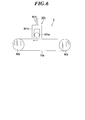
- FIG. 6 is a schematic view of a reforming apparatus for modifying a thin film having an inorganic compound forming a surface layer to form a surface layer.
- reference numeral 5 denotes a reforming apparatus for modifying a thin film containing an inorganic compound to form a surface layer 70c (see FIG. 2).
- the reformer 5 includes a VUV irradiation device 501 and support rolls 502 and 503 that are wound around an endless belt-like base material 70a in which thin films having an elastic layer / inorganic compound are laminated in order from the base material 70a side and rotate in the direction of the arrow. And have.
- the VUV irradiation apparatus 501 includes a reforming chamber 501b having an inert gas supply port 501c and a VUV light source 501a.
- the wavelength of VUV light is preferably 253 nm or less in consideration of the treatment effect, irradiation time, cross-linking density of the film, and the like.
- the inert gas is not particularly limited, and examples thereof include a gas that does not have a large absorption band in the wavelength range of the VUV light source, such as nitrogen gas and argon gas. Nitrogen gas is preferable from the viewpoint of price.
- This figure shows the case where the inside of the VUV irradiation apparatus 501 is filled with an inert gas, but it is of course possible to use a system in which the entire reformer is filled with an inert gas.
- the reformer 5 When using the reformer 5 to irradiate a thin film having an inorganic compound with VUV light, it is preferably performed under the following conditions.
- the oxygen concentration in the inert gas is preferably 1.0% or less, more preferably 0.5% or less in consideration of absorption of the VUV light by the oxygen gas.
- the oxygen concentration in the inert gas can be adjusted by the gas supply amount.
- the oxygen concentration is a value measured by LC-450D manufactured by Toray Engineering Co., Ltd.
- the water concentration in the inert gas is preferably less than general industrial nitrogen gas (about 40 ppm (vol.)).
- the treatment effect is suppressed. More preferably, the humidity is adjusted to less than 60% (temperature is room temperature). It is preferable to maintain the same environment around the processing apparatus because a stable processing effect can be obtained.
- the irradiation treatment with VUV light is sufficient at normal room temperature because the influence of temperature is small, but from the viewpoint of preventing moisture adsorption on the surface to be processed, the temperature of the surface of the belt to be processed is preferably equal to or higher than the processing environment and the apparatus temperature.
- the distance between the VUV light source 501a and the thin film containing an inorganic compound is in principle smaller because the attenuation of light is small, it is preferable to keep the distance between 0.5 mm and 3 mm in consideration of the ease of gap management.
- the treatment effect is determined by the integrated illuminance based on the irradiation intensity and the irradiation time
- the irradiation intensity can be arbitrarily set.
- 10 mW / cm 2 to 300 mW / cm 2 is preferable.
- Irradiation intensity indicates a value measured with UV POWER METER C8026 manufactured by Hamamatsu Photonics.
- the degree of modification of a thin film having an inorganic compound is determined by the integrated illuminance determined by the irradiation intensity and the irradiation time, so that the inorganic compound (metal oxide, metal nitride, metal oxidation) constituting the thin film having the inorganic compound is determined. It is necessary to determine the irradiation time according to the type of nitride.
- This figure shows the case where there is one VUV irradiation apparatus 501, but a plurality of VUV irradiation apparatuses 501 can be arranged as necessary. It is also possible to enlarge the reforming chamber 501b and arrange a plurality of VUV light sources 501a.
- VUV light source 501a a commercially available excimer lamp light source is preferably used.
- Examples of commercially available excimer lamp light sources include MEUT-1-500 manufactured by MDI Excimer.
- An excimer lamp is generally used as an apparatus for irradiating VUV.
- the present invention is not limited to this, and VUV can also be emitted by DC arc plasma.
- VUV can also be generated by plasma discharge of an inert gas containing carbon monoxide.
- the timing of irradiating VUV may be every layer or after all layers are formed.
- the following method can be used as a method when the reforming apparatus 4 is used and the thin film having an inorganic compound is irradiated with VUV to perform the reforming treatment.
- the integrated illuminance is adjusted so that the reforming process is completed in one rotation for the endless belt-shaped base material 70a in which thin films having an elastic layer / inorganic compound wound around the support rolls 502 and 503 are sequentially laminated from the base material 70a side. how to.
- the integrated illuminance is adjusted so that the endless belt-like base material 70a in which the elastic layer / thin film containing inorganic compound wound around the support rolls 502 and 503 are laminated in order from the base material 70a is rotated a plurality of times to complete the reforming process. How to adjust.
- a vacuum ultraviolet light irradiation apparatus 501 is disposed downstream of the atmospheric pressure plasma CVD apparatus 4 of the atmospheric pressure plasma processing apparatus 3a shown in FIG. It is also possible to do.
- VUV is larger than the interatomic bonding force of most substances, it is known that the bonding of atoms can be cut directly by the action of only photons called photon processes.
- the cross-linking can be made dense by cutting off the silanol groups (Si—OH) on the surface and recombining them as SiO 2 , thereby changing other physical properties. Durability can be improved while keeping the minimum. Further, the surface adsorption of water is suppressed by reducing the number of hydrophilic groups on the surface of the thin film having an inorganic compound (thin film having a metal oxide), and the decrease in surface specific resistance ( ⁇ s) is suppressed. As a result, the transfer voltage is stabilized, and the primary transfer efficiency and the secondary transfer efficiency to the transfer material (for example, paper) are further stabilized.
- the transfer voltage is stabilized, and the primary transfer efficiency and the secondary transfer efficiency to the transfer material (for example, paper) are further stabilized.
- vacuum ultraviolet After forming a surface layer (thin film containing an inorganic compound) of an intermediate transfer belt used in an electrophotographic image forming apparatus having at least one surface layer on a substrate by an atmospheric pressure plasma CVD process, vacuum ultraviolet The following effects can be obtained by forming a surface layer by irradiating and processing light to form a surface layer, and producing an intermediate transfer belt. 1. Maintains the flexibility of the surface layer, and the hardness can be obtained without increasing the film thickness, so durability (flexibility (crack resistance), wear resistance and scratch resistance) can be improved. It became. 2. The irradiation process of vacuum ultraviolet light (VUV light) can achieve a sufficient effect even at room temperature, so it is not exposed to high temperatures like heat treatment. Is possible. 3. Since the thin film containing the inorganic compound of the present invention is very thin, vacuum ultraviolet light irradiation treatment can be performed in a very short time, so that the cost increase is small compared to other treatment methods.
- VUV light vacuum ultraviolet light
- the base material and the material used for the elastic layer constituting the intermediate transfer belt of the present invention will be described.
- the elastic layer is not an essential requirement.
- Base material As materials used for the base material, for example, so-called engineering plastic materials such as polycarbonate, polyphenylene sulfide, polyvinylidene fluoride, polyimide, polyether, ether ketone, ethylene tetrafluoroethylene copolymer, polyamide and polyphenylene sulfide can be used. Among them, at least one selected from polyimide, polycarbonate, polyphenylene sulfide, and polyethylene terephthalate is preferable. Furthermore, it is also possible to use a material obtained by blending a resin material and the following elastic material.
- engineering plastic materials such as polycarbonate, polyphenylene sulfide, polyvinylidene fluoride, polyimide, polyether, ether ketone, ethylene tetrafluoroethylene copolymer, polyamide and polyphenylene sulfide can be used. Among them, at least one selected from polyimide, polycarbonate, polyphenylene sulfide
- the elastic material examples include polyurethane, chlorinated polyisoprene, NBR, chloropyrene rubber, EPDM, hydrogenated polybutadiene, butyl rubber, and silicone rubber. These may be used alone or in combination of two or more.
- polyimide resin is formed by heating polyamic acid that is a precursor of the polyimide resin.
- the polyamic acid can be obtained by dissolving tetracarboxylic dianhydride or an approximately equimolar mixture of its derivative and diamine in an organic polar solvent and reacting in a solution state.
- the content rate of the polyimide-type resin in a resin base material is 51% or more.
- the resin base material is preferably adjusted to an electric resistance value (volume resistivity) from 10 5 ⁇ ⁇ cm to 10 11 ⁇ ⁇ cm by adding a conductive substance to the resin material.
- Carbon black can be used as the conductive substance added to the resin material.
- As carbon black neutral or acidic carbon black can be used.
- the amount of the conductive material used varies depending on the type of the conductive material used, but may be added so that the volume resistance value and the surface resistance value of the intermediate transfer member are within a predetermined range. 10 parts by mass to 20 parts by mass, preferably 10 parts by mass to 16 parts by mass.
- the elastic layer may be provided anywhere on the base material, but is preferably provided between the base material and the surface layer. By providing the elastic layer, it is possible to improve the transfer rate to the transferred surface with unevenness, and to suppress the failure of the void.
- the material used for the elastic layer is not particularly limited, and any rubber material or thermoplastic elastomer can be used.
- styrene-butadiene rubber SBR
- high styrene rubber polybutadiene rubber
- BR polybutadiene rubber
- IIR polyisoprene rubber
- ethylene-propylene copolymer ethylene-propylene copolymer
- CR chloroprene rubber
- EPDM ethylene-propylene-diene rubber
- Butyl rubber silicone rubber, fluorine rubber, nitrile rubber, urethane rubber, acrylic rubber (ACM, ANM), epichlorohydrin rubber and norbornene rubber, among others, chloroprene rubber, nitrile rubber, styrene- It is preferably at least one selected from butadiene rubber, silicone rubber, urethane rubber and ethylene-propylene copolymer. These may be used alone or in combination of two or more.
- thermoplastic elastomer polyester, polyurethane, styrene-butadiene triblock, polyolefin, or the like can be used.
- the elastic layer may be a layer formed using a material obtained by blending a resin material used for the base material and an elastic material.
- a material for silicone rubber a polyorganosiloxane composition containing a vinyl group is used.
- silicone rubber a two-component liquid silicone rubber that can be cured by an addition reaction catalyst or a heat vulcanized silicone rubber that can be vulcanized (cured) by a vulcanizing agent made of a peroxide is used.
- the elastic layer may contain various compounding agents such as a filler, an extended filler, a vulcanizing agent, a colorant, a conductive material, a heat-resistant agent, and a pigment depending on the purpose of use and design of the seamless belt. Can be added.
- the plasticity of a synthetic resin changes with the addition amount etc. of a compounding agent, the thing of 120 or less is used suitably as a plasticity of the rigid resin before hardening.
- the elastic layer can adjust the electric resistance value (volume resistivity) from 10 5 ⁇ ⁇ cm to 10 11 ⁇ ⁇ cm by dispersing a conductive substance in the elastic material.
- the conductive substance added to the elastic layer carbon black, zinc oxide, tin oxide, silicon carbide or the like can be used. As carbon black, neutral or acidic carbon black can be used.
- the amount of the conductive material used varies depending on the type of the conductive material to be used, but may be added so that the volume resistance value and the surface resistance value of the elastic layer are within a predetermined range. On the other hand, it is 10 to 20 parts by mass, preferably 10 to 16 parts by mass.
- Example 1 (Production of intermediate transfer belt No. 101) (Preparation of intermediate transfer belt substrate) A molar ratio of BPDA to PDA using 3,3 ′, 4,4′-biphenyltetracarboxylic dianhydride (hereinafter abbreviated as BPDA) as the acid anhydride and p-phenylenediamine (hereinafter abbreviated as PDA) as the diamine.
- BPDA / PDA was set to 10.5, maintained in an N-methylpyrrolidone solvent at 60 ° C. for 4 hours, and polymerized to prepare a polyamic acid solution. Further, a predetermined amount of conductive carbon black that provides a desired resistance was uniformly mixed and dispersed in the solution. The amount of conductive carbon black added varies not only with the target resistance, but also with differences in production lots, etc., so the amount that was confirmed in advance was used.
- the solution was cast in a mold that can be heated, dried to remove the solvent, and further heated to gradually imidize (400 ° C.) to produce a semiconductive endless belt. .
- a thin film (lower layer (first layer) and upper layer (outermost layer, second layer)) containing an inorganic compound was formed on the prepared substrate using the atmospheric pressure plasma processing apparatus shown in FIG.
- the following lower layer (first layer) mixed gas composition As a material for forming the lower layer (first layer), the following lower layer (first layer) mixed gas composition was used, and the following film forming conditions were used.
- the dielectric covering each electrode of the atmospheric pressure plasma processing apparatus at this time both electrodes facing each other were coated with 1 mm thick alumina by a ceramic spraying process. The electrode gap after coating was set to 0.6 mm.
- the metal base material coated with a dielectric is a stainless steel jacket specification that has a cooling function with cooling water. During discharge, the electrode temperature is controlled with cooling water, and the carbon atom content is 5.0 atomic%.
- the carbon atom content indicates a value measured by the XPS method described in the specification text.
- the surface hardness indicates a value measured by the nanoindentation method described in the specification.
- the thickness indicates a value measured by the X-ray reflectivity method described in the specification text.
- ⁇ Lower layer (first layer) formation conditions > 1st electrode side power supply High frequency power supply manufactured by Applied Electronics Co., Ltd. Frequency 80 kHz Output density 8W / cm 2 Second electrode side power supply High frequency power supply made by Pearl Industrial Co., Ltd. Frequency 13.56MHz Output density 8W / cm 2
- the following upper layer (outermost layer, second layer) mixed gas composition is used, and the upper layer (outermost layer, second layer) is formed by the following film formation Performed under conditions.
- the dielectric covering each electrode of the atmospheric pressure plasma processing apparatus at this time both electrodes facing each other were coated with 1 mm thick alumina by a ceramic spraying process. The electrode gap after coating was set to 1 mm.
- the metal base material coated with a dielectric is a stainless steel jacket specification having a cooling function by cooling water, and is performed while controlling the electrode temperature by cooling water during discharge, and has a surface hardness of 4.5 GPa and a thickness of 200 nm.
- An upper layer (outermost layer, second layer) (SiO 2 ) was formed.
- the surface hardness is a value measured by the nanoindentation method described in the text of the specification.
- the thickness indicates a value measured using “MXP21” (manufactured by Mac Science) by the X-ray reflectivity method described in the specification text.
- ⁇ Upper layer (outermost layer, second layer) formation conditions > 1st electrode side power supply High frequency power supply manufactured by Applied Electronics Co., Ltd. Frequency 80 kHz Output density 10W / cm 2 Second electrode side power supply High frequency power supply made by Pearl Industrial Co., Ltd. Frequency 13.56MHz Output density 10W / cm 2
- Modification treatment by VUV irradiation Using the reforming apparatus shown in FIG. 6, a thin film having an inorganic compound formed under the conditions shown below is irradiated with VUV to perform a modification treatment to form a surface layer to produce an intermediate transfer belt. 101. Incidentally, the oxygen concentration was kept below 0.1% by purging with nitrogen gas between the belt surface and the lamp tube surface.
- VUV light source Xe excimer lamp (MEUT-1-550 manufactured by MDI excimer) Wavelength: 172 nm
- Irradiation intensity 50 mW / cm 2
- Distance between VUV light source and surface of thin film containing inorganic compound 1 mm
- Conveying speed of the substrate on which the thin film having the inorganic compound is formed 5 m / min
- VUV integrated irradiation time 4 sec / cm 2 (converted per unit area)
- Irradiation intensity shows the value measured by Hamamatsu Photonics Co., Ltd.
- UV POWER METER C8026 UV POWER METER C8026.
- Sample No. A thin film (lower layer (first layer) and upper layer (outermost layer, second layer)) having an inorganic compound is formed in the same manner as in 101, and sample no. The same substrate / elastic layer / inorganic compound as 101 was used.
- the toner transfer rate (%) was determined.
- Transfer rate (%) (amount of toner transferred onto test print paper / (amount of toner transferred onto test print paper + amount of residual toner on belt)) ⁇ 100 Evaluation rank of transfer efficiency ⁇ : Transfer rate was 98% or more ⁇ : Transfer rate was 95% or more and less than 98% ⁇ : Transfer rate was 90% or more and less than 95% ⁇ : Transfer rate was less than 90%
- Evaluation rank for filming resistance No filming is observed on the intermediate transfer belt ⁇ : Little filming is observed on the intermediate transfer belt ⁇ : Weak filming is generated on the intermediate transfer belt Is observed, but there is no problem in practical use. ⁇ : Level at which filming is observed around the intermediate transfer belt, causing a problem in practical use.
- Sample No. except that it does not have a surface layer containing an inorganic compound. Comparative sample No. 102 manufactured under the same conditions as in No. 102. In Sample No. 104, the transfer efficiency, scratch resistance and filming are sample No. The result was inferior to 102.
- Sample No. 5 was used except that the modification treatment was performed using ultraviolet light having a wavelength of 365 nm instead of VUV irradiation.
- No. 105 is low temperature and low humidity (10 ° C., 20% RH). Although the same performance as that of No. 102 is shown, the transfer efficiency, scratch resistance and filming in the environment of high temperature and high humidity (30 ° C., 80% RH) are the same. The result was inferior to 101.
- Sample No. In Examples 101 to 105 the intermediate transfer belt was manufactured in the same manner except that the intermediate transfer belt was manufactured using polyphenylene sulfide instead of polyimide resin as the intermediate transfer belt base material. The results shown in Tables 1 and 2 above were obtained. The same result was obtained.
- Example 2 (Preparation of base material) The same substrate as that prepared in Example 1 was prepared.
- Sample No. 201 Production Method [Formation of Thin Film Having Inorganic Compound] A thin film (lower layer (first layer) and upper layer (outermost layer, second layer)) containing an inorganic compound was formed on the prepared base material using the atmospheric pressure plasma processing apparatus shown in FIG.
- the following lower layer (first layer) mixed gas composition As a material for forming the lower layer (first layer), the following lower layer (first layer) mixed gas composition was used, and the following film forming conditions were used.
- the dielectric covering each electrode of the atmospheric pressure plasma processing apparatus at this time both electrodes facing each other were coated with 1 mm thick alumina by a ceramic spraying process. The electrode gap after coating was set to 1 mm.
- the metal base material coated with a dielectric is a stainless steel jacket specification that has a cooling function with cooling water. During discharge, the electrode temperature is controlled with cooling water, and the carbon atom content is 5.0 atomic%.
- ⁇ Lower layer (first layer) formation conditions > 1st electrode side power supply High frequency power supply manufactured by Applied Electronics Co., Ltd. Frequency 80 kHz Output density 10W / cm 2 Second electrode side power supply High frequency power supply made by Pearl Industrial Co., Ltd. Frequency 13.56MHz Output density 10W / cm 2
- the following upper layer (outermost layer, second layer) mixed gas composition is used, and the upper layer (outermost layer, second layer) is formed by the following film formation Performed under conditions.
- the dielectric covering each electrode of the atmospheric pressure plasma processing apparatus at this time both electrodes facing each other were coated with 1 mm thick alumina by a ceramic spraying process. The electrode gap after coating was set to 1 mm.
- the metal base material coated with a dielectric is a stainless steel jacket specification having a cooling function with cooling water, and is performed while controlling the electrode temperature with cooling water during discharge, and has a surface hardness of 4.0 GPa and a thickness of 150 nm.
- An upper layer (outermost layer, second layer) (SiO 2 ) was formed. The surface hardness and thickness are values measured by the same method as in Example 1.
- Each source gas was heated to generate steam, mixed and diluted with a discharge gas and a reaction gas that had been preheated so that the source material did not aggregate in advance, and then supplied to the discharge space.
- ⁇ Upper layer (outermost layer, second layer) formation conditions > 1st electrode side power supply High frequency power supply manufactured by Applied Electronics Co., Ltd. Frequency 80 kHz Output density 10W / cm 2 Second electrode side power supply High frequency power supply made by Pearl Industrial Co., Ltd. Frequency 13.56MHz Output density 10W / cm 2
- Example 1 (Modification treatment by VUV irradiation) Sample No. 1 of Example 1 A thin film having an inorganic compound was subjected to a modification treatment under the same conditions and in the same manner as in 101 to form a surface layer to produce an intermediate transfer belt. 201.
- Sample No. 202 production method production of substrate
- the same substrate as that prepared in Example 1 was prepared.
- a thin film (lower layer (first layer) and upper layer (outermost layer, second layer)) containing an inorganic compound was formed on the prepared substrate using the atmospheric pressure plasma processing apparatus shown in FIG.
- the following upper layer (outermost layer, second layer) mixed gas composition is used, and the upper layer (outermost layer, second layer) is formed by the following film formation Performed under conditions.
- the dielectric covering each electrode of the atmospheric pressure plasma processing apparatus at this time both electrodes facing each other were coated with 1 mm thick alumina by a ceramic spraying process. The electrode gap after coating was set to 1 mm.
- the metal base material coated with a dielectric has a stainless steel jacket specification that has a cooling function by cooling water.
- the electrode temperature is controlled by cooling water, and the upper layer (surface hardness 11 GPa, thickness 150 nm) The outermost layer, the second layer) (SiN x ) was formed.
- the surface hardness and thickness are values measured by the same method as in Example 1.
- ⁇ Upper layer (outermost layer, second layer) mixed gas composition > Discharge gas: helium gas 96.95 vol% Film formation (raw material) gas: Tetramethylsilane 0.05% by volume Reaction gas: Ammonia gas 3.00% by volume Each source gas was heated to generate steam, mixed and diluted with a discharge gas and a reaction gas that had been preheated so that the source material did not aggregate in advance, and then supplied to the discharge space.
- Example 1 (Modification treatment by VUV irradiation) Sample No. 1 of Example 1 A thin film having an inorganic compound was subjected to a modification treatment under the same conditions and in the same manner as in 101 to form a surface layer to produce an intermediate transfer belt. 202.
- Sample No. Production method 203 (Preparation of substrate) The same substrate as that prepared in Example 1 was prepared.
- a thin film (lower layer (first layer) and upper layer (outermost layer, second layer)) containing an inorganic compound was formed on the prepared substrate using the atmospheric pressure plasma processing apparatus shown in FIG.
- the following upper layer (outermost layer, second layer) mixed gas composition is used, and the upper layer (outermost layer, second layer) is formed by the following film formation Performed under conditions.
- the dielectric covering each electrode of the atmospheric pressure plasma processing apparatus at this time both electrodes facing each other were coated with 1 mm thick alumina by a ceramic spraying process. The electrode gap after coating was set to 1 mm.
- the metal base material coated with a dielectric is a stainless steel jacket specification having a cooling function with cooling water, and is performed while controlling the electrode temperature with cooling water during discharge, with a surface hardness of 5.0 GPa and a thickness of 150 nm.
- An upper layer (outermost layer, second layer) (TiO 2 ) was formed. The surface hardness and thickness are values measured by the same method as in Example 1.
- Example 1 (Modification treatment by VUV irradiation) Sample No. 1 of Example 1 A thin film having an inorganic compound was modified by the same method and under the same conditions as in 101 to form a surface layer, and an intermediate transfer belt was manufactured. 203.
- Sample No. Production method 204 (Preparation of substrate) The same substrate as that prepared in Example 1 was prepared.
- a thin film (lower layer (first layer) and upper layer (outermost layer, second layer)) containing an inorganic compound was formed on the prepared substrate using the atmospheric pressure plasma processing apparatus shown in FIG.
- the following upper layer (outermost layer, second layer) mixed gas composition is used, and the upper layer (outermost layer, second layer) is formed by the following film formation Performed under conditions.
- the dielectric covering each electrode of the atmospheric pressure plasma processing apparatus at this time both electrodes facing each other were coated with 1 mm thick alumina by a ceramic spraying process. The electrode gap after coating was set to 1 mm.
- the metal base material coated with a dielectric has a stainless steel jacket specification that has a cooling function with cooling water.
- the electrode temperature is controlled with cooling water, and the upper layer (surface hardness 10 Gpa, thickness 150 nm)
- the outermost layer, the second layer) (Al 2 O 3 ) was formed.
- the surface hardness and thickness are values measured by the same method as in Example 1.
- Example 1 (Modification treatment by VUV irradiation) Sample No. 1 of Example 1 A thin film having an inorganic compound was modified by the same method and under the same conditions as in 101 to form a surface layer, and an intermediate transfer belt was manufactured. 204.
- Sample No. Production method 205 preparation of substrate
- the same substrate as that prepared in Example 1 was prepared.
- a thin film (lower layer (first layer) and upper layer (outermost layer, second layer)) containing an inorganic compound was formed on the prepared substrate using the atmospheric pressure plasma processing apparatus shown in FIG.
- the following upper layer (outermost layer, second layer) mixed gas composition is used, and the upper layer (outermost layer, second layer) is formed by the following film formation Performed under conditions.
- the dielectric covering each electrode of the atmospheric pressure plasma processing apparatus at this time both electrodes facing each other were coated with 1 mm thick alumina by a ceramic spraying process. The electrode gap after coating was set to 1 mm.
- the metal base material coated with a dielectric is a stainless steel jacket specification having a cooling function with cooling water, and is performed while controlling the electrode temperature with cooling water during discharge, and has a surface hardness of 4.0 GPa and a thickness of 150 nm.
- An upper layer (outermost layer, second layer) (In 2 O 3 ) was formed. The surface hardness and thickness are values measured by the same method as in Example 1.
- ⁇ Upper layer (outermost layer, second layer) mixed gas composition > Discharge gas: Argon gas 99.45% by volume Film formation (raw material) gas: Indium acetylacetonate 0.05% by volume Reaction gas: 0.50% by volume of hydrogen gas Each source gas was heated to generate steam, mixed and diluted with a discharge gas and a reaction gas that had been preheated so that the source material did not aggregate in advance, and then supplied to the discharge space.
- Example 1 (Modification treatment by VUV irradiation) Sample No. 1 of Example 1 A thin film having an inorganic compound was subjected to modification treatment under the same conditions and in the same manner as in No. 101 to form a surface layer, and an intermediate transfer belt was produced. 205.
- Example 2 The transfer efficiency, scratch resistance, and filming from 201 to 205 were tested in the same manner as in Example 1 at low temperature and low humidity (10 ° C., 20% RH) and high temperature and high humidity (30 ° C., 80% RH).
- Table 4 shows the results of the low temperature and low humidity (10 ° C., 20% RH) environment evaluated according to the same evaluation rank as in Example 1, and
- Table 5 shows the results of the high temperature and high humidity (30 ° C., 80% RH) environment.
- Example 3 (Preparation of base material) The same substrate as that prepared in Example 1 was prepared.
- VUV light sources having different wavelengths were prepared. From 3-1 to 3-4.
- Example 1 The transfer efficiency, scratch resistance and filming from 301 to 304 were tested in the same manner as in Example 1 at low temperature and low humidity (10 ° C., 20% RH) and high temperature and high humidity (30 ° C., 80% RH).
- Table 7 shows the results of the low temperature and low humidity (10 ° C., 20% RH) environment evaluated in accordance with the same evaluation rank as in Example 1, and
- Table 8 shows the results of the high temperature and high humidity (30 ° C., 80% RH) environment.
- inorganic formed by atmospheric pressure plasma CVD method Sample No. 1 in which the surface layer was formed by changing the wavelength of the VUV light source for modifying the thin film containing the compound at 253 nm or less to form the surface layer and producing the intermediate transfer belt. Nos. 301 to 303 were confirmed to exhibit excellent performance in terms of transfer efficiency, scratch resistance, and filming in environments of low temperature and low humidity (10 ° C., 20% RH) and high temperature and high humidity (30 ° C., 80% RH).
- Sample No. No. 1 was manufactured by forming a surface layer by modifying the VUV light source for modifying the thin film having an inorganic compound formed by the atmospheric pressure plasma CVD method at a wavelength of 308 nm to produce an intermediate transfer belt.
- 304 shows transfer efficiency, scratch resistance and filming in low temperature and low humidity (10 ° C., 20% RH) and high temperature and high humidity (30 ° C., 80% RH) environments, but shows slightly inferior performance. It was confirmed.
- the present invention provides a method for manufacturing an intermediate transfer belt that can form a high-quality image without causing a decrease in transfer efficiency, scratch resistance, and filming resistance even after long-term printing. Is suitable.
Landscapes
- Physics & Mathematics (AREA)
- General Physics & Mathematics (AREA)
- Electrostatic Charge, Transfer And Separation In Electrography (AREA)
Abstract
基材70aの上に少なくとも1層の表面層70cを設けた電子写真方式の画像形成装置に使用する中間転写ベルトの製造方法において、表面層70aは、無機化合物を有する膜を基材の上に設けた後、膜に真空紫外光を照射し形成される。
Description
本発明は、電子写真複写機、プリンター等の電子写真方式の画像形成装置に用いられる中間転写ベルトの製造方法に関するものである。
電子写真方式の画像形成装置においては、その装置内において様々な機能、用途でシームレスベルト部材が用いられている。例えば、定着ベルト、転写ベルト、紙搬送ベルト等が挙げられる。
電子写真方式の画像形成装置は、帯電したトナーを感光体上の静電潜像に接触或いは非接触で供給し、静電潜像を顕像にする現像過程を経て形成したトナー像を転写工程で転写部材である中間転写体に一次転写した後、転写材(例えば紙)に二次転写し、更に定着部材により定着して最終画像を形成するものである。
電子写真方式の画像形成装置においては、感光体(像担持体)上に形成された4色のトナー画像を、一旦中間転写体に転写(一次転写)することにより、中間転写体上にフルカラー画像を形成し、その後に紙などの転写媒体(記録媒体)に一括転写(二次転写)する中間転写体方式が主流となりつつある。中間転写体としては、無端状ベルト部材を使用した中間転写ベルト、管状部材を使用した中間転写ロールが使用されており、フルカラー画像形成装置においては、高速性を得るため、中間転写体に対峙する各色の色現像装置を直列に配置したタンデム方式といわれる方式が主流となっており、機構上から中間転写ベルトが多く使用されている。
高画質フルカラー化、高品質化の要求に対して管状物である中間転写ベルト方式の課題として、感光体上のトナー画像を中間転写ベルトへ一次転写する時の一次転写性(一次転写効率)、及び中間転写ベルト上のトナー画像を記録媒体へ二次転写する時の二次転写性(二次転写効率)が不安定になることが挙げられる。尚、本発明では、一次転写性、二次転写性を含めて転写性と言う。
中間転写ベルト方式には次の問題点が挙げられる。
1.中間転写ベルト上に残ったトナーの除去や転写媒体(記録媒体)への二次転写での接触に伴い中間転写ベルト表面に傷が付き、スジ状の画像ムラが発生する。
2.中間転写ベルト上に残ったトナーの除去残りがあると、色むらやかぶりのような異常画像が発生する。また、フィルミングによる耐久性の劣化要因となる。
3.中間転写ベルト上に残ったトナーを除去に伴い中間転写ベルト表面に傷が付き、トナー除去残りなどが発生しやすくなることから中間転写ベルトの寿命に影響する。
1.中間転写ベルト上に残ったトナーの除去や転写媒体(記録媒体)への二次転写での接触に伴い中間転写ベルト表面に傷が付き、スジ状の画像ムラが発生する。
2.中間転写ベルト上に残ったトナーの除去残りがあると、色むらやかぶりのような異常画像が発生する。また、フィルミングによる耐久性の劣化要因となる。
3.中間転写ベルト上に残ったトナーを除去に伴い中間転写ベルト表面に傷が付き、トナー除去残りなどが発生しやすくなることから中間転写ベルトの寿命に影響する。
このため高画質フルカラー化、高品質化の要求に対して耐摩耗性、耐クリープ性、寸法安定性、耐久性、耐傷性に優れ、感光体や用紙等の転写媒体の表面性状によらず高い転写率及び転写性能を発現し、中抜けや濃度むら、色むらのような異常画像が発生しないことを目的とした中間転写ベルトの検討がされてきた。例えば、基材上に設ける高画質な転写効率に有効な弾性層の厚みの調整、耐摩耗性に有効なダイヤモンド微粒子を含有する樹脂層からなる表面層の厚みの調整、ダイヤモンド微粒子の含有量の調整等を行うことで、高画質な転写効率と耐磨耗性を満たす中間転写ベルトを得ることが知られている(例えば、特許文献1参照)。
しかしながら、複数のロールに懸架され巻回され、また、感光体、転写材(紙、フィルムなど)、転写後の残存トナーを除去するためのクリーニング部材との接触に伴い、屈曲(延ばし方向、縮ませ方向)負荷、押し込み負荷、摩擦摩耗負荷が長期間繰り返し加えられると、特許文献1に記載の中間転写ベルトでは、転写効率と耐磨耗性が両立する寿命は、弾性層厚み、ダイヤモンド微粒子含有量、ダイヤモンド微粒子を含む表面層厚みを調整しないものに比べて、伸びると思われるが、長期間プリントを行う過程では、表面層からのダイヤモンド微粒子の脱落、クラックや擦り傷の発生、フィルミングの発生、ダイヤモンド微粒子が脱落した凹みに異物やトナーなどの成分が付着することにより、長期間プリントをする過程で、高画質な転写効率、クラック耐性、擦り傷耐性と耐磨耗性を満足することは到底出来ないものとなることが判った。
又、基層上にトナー中に含まれる油分(ワックス成分)との離型性向上に有効なn-ドデカン接触角を20°以上とし、層の表面の傷防止に有効な鉛筆硬度4H以上のハードコート層を設けることで高画質な転写効率を得る中間転写ベルトを得ることが知られている(例えば、特許文献2参照)。
しかしながら、複数のロールに懸架され巻回され、また、感光体、転写材(紙、フィルムなど)、転写後の残存トナーを除去するためのクリーニング部材との接触に伴い、屈曲(延ばし方向、縮ませ方向)負荷、押し込み負荷、摩擦摩耗負荷が長期間繰り返し加えられると、特許文献2に記載の中間転写ベルトでは、クラック、擦り傷、表面層の削れが発生してしまい高画質な転写効率が保てず、改善のために、表面層厚みを厚くすると屈曲(延ばし方向、縮ませ方向)負荷によって、クラックが発生してしまう。
又、接触するトナー中の成分や接触する紙から発生する紙粉、転写部内に持ち込まれる異物などが付着し、取り除くためにプリント後に行う中間転写ベルトのクリーニング強化により擦り傷が発生してしまい、傷の発生防止と異物付着防止との両立が困難となり、長期間プリントをする過程で、高画質な転写効率、クラック耐性、擦り傷耐性と耐磨耗性を満足することは到底出来ないものとなることが判った。
この様な状況から、長期間プリントをしても転写効率、擦り傷耐性、フィルミング耐性の低下が発生することなく、高品質の画像を形成することが出来る中間転写ベルトの製造方法の開発が望まれている。
本発明は、上記状況に鑑みなされたものであり、その目的は長期間プリントをしても転写効率、擦り傷耐性、フィルミング耐性の低下が発生することなく、高品質の画像を形成することが出来る中間転写ベルトの製造方法を提供することである。
本発明の上記目的は、下記の構成で達成された。
1.基材の上に少なくとも1層の表面層を設けた電子写真方式の画像形成装置に使用する中間転写ベルトの製造方法において、
前記表面層は、無機化合物を有する膜を前記基材の上に設けた後、前記膜に真空紫外光を照射し形成されることを特徴とする中間転写ベルトの製造方法。
前記表面層は、無機化合物を有する膜を前記基材の上に設けた後、前記膜に真空紫外光を照射し形成されることを特徴とする中間転写ベルトの製造方法。
2.前記無機化合物を有する膜を大気圧プラズマCVD処理により設けることを特徴とする前記1に記載の中間転写ベルトの製造方法。
3.前記無機化合物が酸化ケイ素又はSiOαC2-α(α=1.5から2.0)であることを特徴とする前記1または2に記載の中間転写ベルトの製造方法。
4.前記表面層は、基材上に2層以上設けられることを特徴とする前記1から3の何れか1項に記載の中間転写ベルトの製造方法。
5.前記2層以上の表面層のうち、前記基材から最も離れて設けられる表面層の炭素含有率が0.1原子数濃度%以下であることを特徴とする前記4に記載の中間転写ベルトの製造方法。
6.前記真空紫外光を照射する雰囲気の不活性ガス中の酸素濃度が1.0%以下であることを特徴とする前記1から5の何れか1項に記載の中間転写ベルトの製造方法。
7.前記真空紫外光の波長が、253nm以下であることを特徴とする前記1から6の何れか1項に記載の中間転写ベルトの製造方法。
8.前記真空紫外光の照射を前記2層以上の表面層の全ての層を設けた後に行うことを特徴とする前記4から7の何れか1項に記載の中間転写ベルトの製造方法。
本発明者らは、先に記載したように長期間プリントをしても高画質な転写効率を継続するには、以下の要件が必要であることを見出した。
1)クラック、擦り傷、異物付着、フィルミングなどの欠陥の原因となる粒子状物質(ダイヤモンド粒子、無機物粒子、有機物粒子など)を表面層に含有させないこと。
2)クラック、擦り傷、表面層の削れを発生させず、かつ、屈曲(延ばし方向、縮ませ方向)負荷によってもクラックが発生させないためには、高硬度な表面層を薄く形成すること。
3)紙粉や異物などの付着を抑制するためには表面層が平滑であること。
1)クラック、擦り傷、異物付着、フィルミングなどの欠陥の原因となる粒子状物質(ダイヤモンド粒子、無機物粒子、有機物粒子など)を表面層に含有させないこと。
2)クラック、擦り傷、表面層の削れを発生させず、かつ、屈曲(延ばし方向、縮ませ方向)負荷によってもクラックが発生させないためには、高硬度な表面層を薄く形成すること。
3)紙粉や異物などの付着を抑制するためには表面層が平滑であること。
又、無機化合物を有する薄膜で構成された表面層の懸念点として、表面層の架橋密度が不足している場合は、プリントする環境湿度が変化すると転写効率が変化したり画質ムラが発生する可能性があるため、長期間プリントする過程で高画質な転写効率を維持出来ない可能性がある。
よって、本発明者らはプリントする環境湿度が変化すると転写効率が変化したり画質ムラが発生する場合の原因を解析した結果、無機化合物を有する薄膜中に親水性基が残留していることが判り、残留している親水性基を減少させるには、無機化合物を有する薄膜の架橋密度を上げることが必要で、無機化合物を有する薄膜に対し真空紫外光の照射処理を行なうことで、薄膜の架橋密度が増加し、プリントする環境湿度が変化しても、転写効率が変化しない中間転写ベルトを形成出来ることを見出し本発明に至った次第である。
長期間プリントをしても転写効率、擦り傷耐性、フィルミング耐性の低下が発生することなく、高品質の画像が形成することが出来る中間転写ベルトの製造方法を提供することが出来た。
本発明の実施の形態を図1から図6を参照しながら説明するが、本発明はこれに限定されるものではない。
図1は、中間転写体として中間転写ベルトを使用した電子写真方式の画像形成装置の一例を示す概略断面構成図である。尚、本図はフルカラー画像形成装置の場合を示している。
図中、1はフルカラー画像形成装置を示す。フルカラー画像形成装置1は、複数組の画像形成ユニット10Y、10M、10C、10Kと、転写部としての無端ベルト状中間転写体形成ユニット7と、記録媒体Pを搬送する無端ベルト状の給紙搬送手段21及び定着手段としてのベルト式定着装置24とを有する。フルカラー画像形成装置1の本体Aの上部には、原稿画像読み取り装置SCが配置されている。
各感光体1Y、1M、1C、1Kに形成される異なる色のトナー像の1つとして、イエロー色の画像を形成する画像形成ユニット10Yは、第1の像担持体としてのドラム状の感光体1Y、感光体1Yの周囲に配置された帯電手段2Y、露光手段3Y、現像剤担持体4Y1を有する現像手段4Y、一次転写手段としての一次転写ローラー5Y、クリーニング手段6Yを有する。
又、別の異なる色のトナー像の1つとして、マゼンタ色の画像を形成する画像形成ユニット10Mは、第1の像担持体としてのドラム状の感光体1M、感光体1Mの周囲に配置された帯電手段2M、露光手段3M、現像剤担持体4M1を有する現像手段4M、一次転写手段としての一次転写ローラー5M、クリーニング手段6Mを有する。
又、更に別の異なる色のトナー像の1つとして、シアン色の画像を形成する画像形成ユニット10Cは、第1の像担持体としてのドラム状の感光体1C、感光体1Cの周囲に配置された帯電手段2C、露光手段3C、現像剤担持体4C1を有する現像手段4C、一次転写手段としての一次転写ローラー5C、クリーニング手段6Cを有する。
又、更に他の異なる色のトナー像の1つとして、黒色画像を形成する画像形成ユニット10Kは、第1の像担持体としてのドラム状の感光体1K、感光体1Kの周囲に配置された帯電手段2K、露光手段3K、現像剤担持体4K1を有する現像手段4K、一次転写手段としての一次転写ローラー5K、クリーニング手段6Kを有する。
無端ベルト状中間転写体形成ユニット7は、複数のローラーにより巻回され、回動可能に支持された半導電性エンドレスベルト状の第2の像担持体として無端の中間転写ベルト70を有する。
画像形成ユニット10Y、10M、10C、10Kより形成された各色の画像は、一次転写ローラー5Y、5M、5C、5Kにより、回動する無端の中間転写ベルト70上に逐次転写されて、合成されたカラー画像が形成される。給紙カセット20内に収容された記録媒体として用紙等の記録媒体Pは、給紙搬送手段21により給紙され、複数の中間ローラー22A、22B、22C、22D、レジストローラー23を経て、二次転写手段としての二次転写ローラー5Aに搬送され、記録媒体P上にカラー画像が一括転写される。
カラー画像が転写された記録媒体Pは、熱ローラー定着器270が装着された定着装置24により定着処理され、排紙ローラー25に挟持されて機外の排紙トレイ26上に載置される。
一方、二次転写ローラー5Aにより記録媒体Pにカラー画像を転写した後、記録媒体Pを曲率分離した無端の中間転写ベルト70は、クリーニング手段6Aにより残留トナーが除去される。
画像形成処理中、一次転写ローラー5Kは常時、感光体1Kに圧接している。他の一次転写ローラー5Y、5M、5Cはカラー画像形成時にのみ、それぞれ対応する感光体1Y、1M、1Cに圧接する。
二次転写ローラー5Aは、ここを記録媒体Pが通過して二次転写が行われる時にのみ、無端の中間転写ベルト70に圧接する。
又、装置本体Aから筐体8を支持レール82L、82Rを介して引き出し可能にしてある。筐体8は、画像形成ユニット10Y、10M、10C、10Kと、無端ベルト状中間転写体形成ユニット7とを有する。
画像形成ユニット10Y、10M、10C、10Kは、垂直方向に縦列配置されている。感光体1Y、1M、1C、1Kの図示左側方には無端ベルト状中間転写体形成ユニット7が配置されている。無端ベルト状中間転写体形成ユニット7は、ローラー71、72、73、74、76を巻回して回動可能な無端の中間転写ベルト70、一次転写ローラー5Y、5M、5C、5K及びクリーニング手段6Aとを有している。
筐体8の引き出し操作により、画像形成ユニット10Y、10M、10C、10Kと、無端ベルト状中間転写体形成ユニット7とは、一体となって、本体Aから引き出される。
この様に感光体1Y、1M、1C、1Kの外周面上を帯電、露光し外周面上に潜像を形成した後、現像によりトナー像(顕像)を形成し、無端の中間転写ベルト70上で各色のトナー像を重ね合わせ、一括して記録媒体Pに転写し、ベルト式定着装置24で加圧及び加熱により固定して定着する。尚、本発明で像形成時とは潜像形成、トナー像(顕像)を記録媒体Pに転写し最終画像を形成することを含む。
トナー像を記録媒体Pに転移させた後の感光体1Y、1M、1C、1Kは、各感光体1Y、1M、1C、1Kに配設されたクリーニング手段6Y、6M、6C、6Kで転写時に感光体に残されたトナーを清掃した後、上記の帯電、露光、現像のサイクルに入り、次の像形成が行われる。
上記カラー画像形成装置では、中間転写ベルトをクリーニングするクリーニング手段6Aのクリーニング部材として、弾性ブレードを用いる。又、各感光体に脂肪酸金属塩を塗布する手段(11Y、11M、11C、11K)を設けている。尚、脂肪酸金属塩としては、トナーで用いたと同じものを用いることが出来る。
本発明は、長期間プリントをしても転写効率、擦り傷耐性、フィルミング耐性の低下が発生することなく画質の変動が小さく保てる中間転写ベルトの製造方法、中間転写ベルト及び中間転写ベルトを使用した画像形成装置に関するものである。尚、長期間プリントとは、100万枚程度のプリントを行うことを言う。
図2は図1に示す中間転写ベルトの拡大概略断面図である。
図中、70は中間転写ベルトを示す。中間転写ベルト70は、基材70aの上に順次弾性層70bと、表面層70cとを積層した構成を有している。
基材70aは従来公知の一般的な方法により製造することが可能である。例えば材料となる樹脂を押出機により溶融し、環状ダイを使用したインフレーション法により筒状に成形した後、輪切りにすることで環状の無端ベルト状の基材を作製することが出来る。
基材70aのヤング率は、クリーニング部材であるクリーニングブレードから中間転写ベルトに加わる負荷に伴う変形、連続して巻回しによる使用に耐える柔軟性等を考慮し、ナノインデンテーション法により測定したヤング率が5.0GPaから15.0GPaが好ましい。
弾性層70bは公知の塗布方法、例えば特開2006-255615号公報に記載の浸漬塗布、特開平10-104855号公報に記載の円形量規制型塗布、特開2007-136423号公報に記載の環状塗布方法、或いは浸漬塗布と円形量規制型塗布を組み合わせて塗膜を設けて作製することが出来る。
弾性層はJIS A硬度で40°から70°、弾性率は、基材或いは好ましい態様の1つである樹脂層の弾性率にもよるが、強度およびニップ性等を考慮し、引張り弾性率1×10⁵から1×10⁷Pa(JIS K7161)であることが好ましい。
ナノインデンテーション法により測定したヤング率で表すと2.0GPa未満が好ましい。
また、弾性層の炭素含有率は、後述するXPS法により算出され、25原子数濃度%以上であることが好ましい。
ナノインデンテーション法により測定したヤング率で表すと2.0GPa未満が好ましい。
また、弾性層の炭素含有率は、後述するXPS法により算出され、25原子数濃度%以上であることが好ましい。
表面層70cは無機化合物を有する薄膜を弾性層70bの上に形成した後、真空紫外光(Vacuum Ultraviolet:VUV)線を照射し無機化合物を有する薄膜が改質処理されることで形成されている。尚、無機化合物を有する薄膜の形成は特に限定されず、例えば大気圧プラズマCVD法、真空プラズマCVD法、光CVD法、熱CVD法、真空蒸着法、スパッタ法、溶射法、ウエット塗布法等が挙げられが、これらの中では大気圧プラズマCVD法が好ましい。大気圧プラズマCVD法による表面層70cの形成方法の詳細は図3から図6で説明する。
又、本図では表面層70cが1層の場合を示しているが必要に応じて2層以上で構成しても構わない。弾性層70bは必要に応じて設けることが可能である。又、必要に応じて弾性層70bと表面層70cとの間に樹脂層を設けることが可能である。
Eは基材70aの厚さを示す。厚さEは、機械的強度、画質、製造コスト等を考慮し、50μmから1000μmが好ましい。より好ましくは50μmから200μmである。
Fは弾性層70bの厚さを示す。厚さFは、画質、耐久性等を考慮し、50μmから500μmが好ましい。より好ましくは100μmから300μmである。
Gは表面層70cの厚さを示す。厚さGは、耐久性、表面強度、下層との密着性、屈曲耐性、成膜時間等を考慮し、50nmから1000nmが好ましい。より好ましくは200nmから500nmである。
表面層70cの膜厚は、X線反射率法で「MXP21」(マックサイエンス社製)を用いて測定して得られた値である。具体的な膜厚の測定は、以下の方法で行うことができる。X線源のターゲットには銅を用い、42kV、500mAで作動させる。インシデントモノクロメータには多層膜パラボラミラーを用いる。入射スリットは0.05mm×5mm、受光スリットは0.03mm×20mmを用いる。2θ/θスキャン方式で0から5°をステップ幅0.005°、1ステップ10秒のFT法にて測定を行う。得られた反射率曲線に対し、マックサイエンス社製Reflectivity Analysis Program Ver.1を用いてカーブフィッティングを行い、実測値とフィッティングカーブの残差平方和が最小になるように各パラメータを求める。各パラメータから積層膜の膜厚を求める。
表面層70cが2層以上の場合、最表層の厚さは、5nm以上、200nm以下であることが好ましく、更には10nm以上、100nm以下であることが好ましい。また、最表層を除く、他の表面層70c全体の膜厚は100nm以上、1000nm以下であることが好ましく、更には200nm以上、700nm以下であることが好ましい。この様にすることで、更なる耐久効果が得られる。
尚、基材70a及び弾性層70bの厚さは、(株)ミツトヨ製マイクロメータで測定した値を示す。
(表面層の硬度)
表面層70cの硬度はナノインデンテーション法により測定することが可能である。ナノインデンテーション法とは、試料に対して超微小な荷重で圧子を連続的に負荷、除荷し、得られた荷重-変位曲線から硬さ(Hardness、以下、Hと略記)を測定する方法である。
表面層70cの硬度はナノインデンテーション法により測定することが可能である。ナノインデンテーション法とは、試料に対して超微小な荷重で圧子を連続的に負荷、除荷し、得られた荷重-変位曲線から硬さ(Hardness、以下、Hと略記)を測定する方法である。
ナノインデンテーションの硬さ(H)は、試料の直接的な表面の硬さの値を表している。従って、ナノインデンテーションの硬さ(H)が表面硬度の指標として適している。
〈ナノインデンテーション法による硬度(H)の測定〉
表面層70cのナノインデンテーション法による硬度(H)の測定は、Hysitron社製TriboscopeをDigital Instruments社製NanoscopeIIIに試料を装着し測定した。測定には、圧子としてベルコビッチ型圧子(先端稜角142.3°)と呼ばれる三角錘型ダイヤモンド製圧子を用いる。
表面層70cのナノインデンテーション法による硬度(H)の測定は、Hysitron社製TriboscopeをDigital Instruments社製NanoscopeIIIに試料を装着し測定した。測定には、圧子としてベルコビッチ型圧子(先端稜角142.3°)と呼ばれる三角錘型ダイヤモンド製圧子を用いる。
三角錘型ダイヤモンド製圧子を試料表面に直角に当て、徐々に荷重を印加し、最大荷重到達後に荷重を0にまで徐々に戻した。この時の最大荷重Pを圧子接触部の投影面積Aで除した値P/Aを硬度(H)として算出した。この時の最大荷重の条件は100μNで行う。尚、ナノインデンテーション法による表面硬度測定の原理に関する詳細は、例えば、Handbook of Micro/Nano Tribology(Bharat Bhushan編 CRC)に記載されている。
〈表面層の炭素含有率〉
又、本発明の中間転写体においては、表面層70cが2層以上で構成される場合、下層の炭素含有率が、隣接する上層の炭素含有率よりも高い構成をとることが好ましく、更には最表層を除く表面層70cの炭素含有率(炭素原子数濃度)としては0.5原子数濃度%から10原子数濃度%、最表層の炭素含有率(炭素原子数濃度)は0.1原子数濃度%以下であることが好ましい。
又、本発明の中間転写体においては、表面層70cが2層以上で構成される場合、下層の炭素含有率が、隣接する上層の炭素含有率よりも高い構成をとることが好ましく、更には最表層を除く表面層70cの炭素含有率(炭素原子数濃度)としては0.5原子数濃度%から10原子数濃度%、最表層の炭素含有率(炭素原子数濃度)は0.1原子数濃度%以下であることが好ましい。
本発明でいう炭素含有率を示す原子数濃度とは、下記のXPS法によって算出されるもので、以下に定義される。
原子数濃度%(atomic concentration)=炭素原子の個数/全原子の個数×100
XPS表面分析装置は、本発明では、VGサイエンティフィックス社製ESCALAB-200Rを用いた。具体的には、X線アノードにはMgを用い、出力600W(加速電圧15kV、エミッション電流40mA)で測定した。エネルギー分解能は、清浄なAg3d5/2ピークの半値幅で規定したとき、1.5eVから1.7eVとなるように設定した。
XPS表面分析装置は、本発明では、VGサイエンティフィックス社製ESCALAB-200Rを用いた。具体的には、X線アノードにはMgを用い、出力600W(加速電圧15kV、エミッション電流40mA)で測定した。エネルギー分解能は、清浄なAg3d5/2ピークの半値幅で規定したとき、1.5eVから1.7eVとなるように設定した。
測定としては、先ず、結合エネルギー0eVから1100eVの範囲を、データ取り込み間隔1.0eVで測定し、いかなる元素が検出されるかを求めた。
次に、検出された、エッチングイオン種を除く全ての元素について、データの取り込み間隔を0.2eVとして、その最大強度を与える光電子ピークについてナロースキャンをおこない、各元素のスペクトルを測定した。
得られたスペクトルは、測定装置、あるいは、コンピュータの違いによる含有率算出結果の違いを生じせしめなくするために、VAMAS-SCA-JAPAN製のCOMMON DATA PROCESSING SYSTEM (Ver.2.3以降が好ましい)上に転送した後、同ソフトで処理をおこない、各分析ターゲットの元素(炭素、酸素、ケイ素、チタン等)の含有率の値を原子数濃度(atomic concentration:at%)として求めた。
定量処理を行う前に、各元素についてCount Scaleのキャリブレーションを行い、5ポイントのスムージング処理を行った。定量処理では、バックグラウンドを除去したピークエリア強度(cps*eV)を用いた。バックグラウンド処理には、Shirleyによる方法を用いた。このShirley法については、D.A.Shirley,Phys.Rev.,B5,4709(1972)を参考にすることができる。
図3は中間転写ベルトの表面層70c(図2参照)を形成する無機化合物を有する薄膜を大気圧プラズマCVD法により形成る大気圧プラズマ処理装置の概略図である。尚、大気圧プラズマCVD法とは、大気圧もしくはその近傍の圧力下で行われるプラズマCVD法を言う。大気圧もしくはその近傍の圧力とは20kPaから110kPa程度であり、本発明では93kPaから104kPaが好ましい。
図中、3aは大気圧プラズマ処理装置を示す。大気圧プラズマ処理装置3aは、無端ベルト状の基材70aを巻架して矢印方向に回転するロール電極30と、従動ローラー301と、無端ベルト状の基材70aの表面に無機化合物層を有する薄膜を形成する複数の大気圧プラズマCVD装置4とを有している。尚、本図では無端ベルト状の基材70aとは図2に示す弾性層70bを積層した状態を言う。
大気圧プラズマCVD装置4は、ロール電極30の外周に沿って配列された少なくとも1式の固定電極31と、固定電極31とロール電極30との対向領域で且つ放電が行われる放電空間33と、少なくとも原料ガスと放電ガスとの混合ガスGを生成して放電空間33に混合ガスGを供給する混合ガス供給装置34と、放電空間33等に空気の流入することを軽減する放電容器39と、ロール電極30に接続された第1の電源35と、固定電極31に接続された第2の電源36と、使用済みの排ガスG’を排気する排気部38とを有している。
混合ガス供給装置34は無機化合物を有する薄膜として、無機酸化物を有する薄膜、無機窒化物を有する薄膜の何れかを形成する原料ガスと、窒素ガス或いはアルゴンガス等の希ガスを混合した混合ガスを放電空間33に供給する。また、酸化還元反応による反応促進のための酸素ガスまたは水素ガスを混合することがより好ましい。
又、従動ローラー301は張力付与手段302により矢印方向に牽引され、基材70aに所定の張力を掛けている。張力付与手段302は基材70aの掛け替え時等は張力の付与を解除し、容易に基材70aの掛け替え等を可能としている。
第1の電源35は周波数ω1の電圧を出力し、第2の電源36は周波数ω2の電圧を出力し、これらの電圧により放電空間33に周波数ω1とω2とが重畳された電界Vを発生する。そして、電界Vにより混合ガスGをプラズマ化して混合ガスGに含まれる原料ガスに応じた無機化合物を有する薄膜が基材70aの表面に堆積される。基材70aの表面とは弾性層70bの表面を言う。
尚、複数の固定電極の内、ロール電極の回転方向下流側に位置する複数の固定電極と混合ガス供給装置で無機化合物を有する薄膜を積み重ねるように堆積し、無機化合物を有する薄膜の厚さを調整するようにしても良い。
又、複数の固定電極31の内、ロール電極30の回転方向最下流側に位置する固定電極31と混合ガス供給装置34で無機化合物を有する薄膜を堆積し、より上流に位置する他の固定電極と混合ガス供給装置で、例えば無機化合物を有する薄膜と弾性層70bとの接着性を向上させる接着層等、他の層を形成してもよい。
又、基材70aと弾性層70bとの接着性を向上させるために、無機化合物を有する薄膜を形成する固定電極31と混合ガス供給装置34の上流に、アルゴンや酸素などのガスを供給するガス供給装置(不図示)と固定電極(不図示)を設けてプラズマ処理を行い、基材70aの表面を活性化させるようにしても良い。
以上説明したように、無端ベルト状の基材70aをロール電極30と従動ローラー301とに張架し、ロール電極20の外周面の外側に沿って他方の電極である少なくとも1の固定電極31を設け、原料ガスと、窒素ガス或いはアルゴンガス等の希ガスを混合した混合ガスを放電空間33に供給し、ロール電極30と固定電極31間に大気圧または大気圧近傍下で電界を発生させプラズマ放電を行わせることで、無端ベルト状の基材70aの表面に無機化合物を有する薄膜を形成することが可能となっている。
尚、本図に示す大気圧プラズマ処理装置を真空環境に設置することで真空プラズマ処理装置として使用することが可能である。但し、窒素ガス或いはアルゴンガス等の希ガスは使用しなくてもよい。
図4は、中間転写ベルトの表面層を形成する無機化合物を有する薄膜を形成する大気圧プラズマCVD法による他の大気圧プラズマ処理装置の概略図である。
3bは大気圧プラズマ処理装置を示す。大気圧プラズマ処理装置3bは複数の基体上に同時に無機化合物を有する薄膜を形成するもので、主として基体表面に無機化合物を有する薄膜を形成する複数の大気圧プラズマCVD装置3b1及び大気圧プラズマCVD装置3b2より構成されている。
大気圧プラズマ処理装置3bは、大気圧プラズマCVD装置3b1と所定の間隙を隔てて略鏡像関係に配置された大気圧プラズマCVD装置置3b2と、大気圧プラズマCVD装置3b1と大気圧プラズマCVD装置3b2との間に配置された少なくとも原料ガスと放電ガスとの混合ガスGを生成して放電空間33bに混合ガスGを供給する混合ガス供給装置34bとを有している。
大気圧プラズマCVD装置3b1は無端ベルト状の基材70aを巻架して矢印方向に回転するロール電極30aと従動ローラー301aと矢印方向に従動ローラー301aを牽引する張力付与手段302aとロール電極30aに接続された第1の電源35とを有している。
大気圧プラズマCVD装置3b2は無端ベルト状の基材70aを巻架して矢印方向に回転するロール電極30bと従動ローラー301bと矢印方向に従動ローラー301bを牽引する張力付与手段302bとロール電極30bに接続された第2の電源36とを有している。尚、本図では無端ベルト状の基材70aとは図2に示す弾性層を積層した状態を言う。
又、大気圧プラズマ処理装置3bはロール電極30aとロール電極30bとの対向領域に放電が行われる放電空間33bを有している。
混合ガス供給装置34bは無機化合物を有する薄膜として無機酸化物を有する薄膜、無機窒化物を有する薄膜から選ばれる少なくとも1つの薄膜を形成する原料ガスと、窒素ガス或いはアルゴンガス等の希ガスを混合した混合ガスを放電空間33bに供給する。また、酸化還元反応による反応促進のための酸素ガスまたは水素ガスを混合することがより好ましい。
第1の電源35は周波数ω1の電圧を出力し、第2の電源36は周波数ω2の電圧を出力し、これらの電圧により放電空間33bに周波数ω1とω2とが重畳された電界Vを発生する。そして、電界Vにより混合ガスGをプラズマ化(励起)し、プラズマ化(励起)した混合ガスを大気圧プラズマCVD装置3b1の基材70a及び大気圧プラズマCVD装置3b2の基材70aの表面に晒し、プラズマ化(励起)した混合ガスに含まれる原料ガスに応じた無機化合物を有する薄膜が大気圧プラズマCVD装置3b1の基材70a及び大気圧プラズマCVD装置3b2の基材70aの表面に同時に堆積・形成される。基材70aの表面とは弾性層の表面を言う。
ここで、対向するロール電極30aとロール電極30bとは所定の間隙を隔てて配置されている。
尚、本図に示す大気圧プラズマ処理装置を真空環境に設置することで真空プラズマ処理装置として使用することが可能である。但し、窒素ガス或いはアルゴンガス等の希ガスは使用しなくてもよい。
図5は図3のPで示される部分の拡大概略図である。
大気圧プラズマCVD装置4は、混合ガス供給装置34、固定電極31、第1の電源35、第1のフィルター35a、ロール電極30、ロール電極を矢印方向に駆動回転させる駆動手段30a、第2の電源36、第2のフィルター36aとを有しており、放電空間33でプラズマ放電を行わせて原料ガスと放電ガスを混合した混合ガスGを励起させ、励起した混合ガスG1を基材70aの上に形成された弾性層70bの表面に晒し、その表面に無機化合物を有する薄膜を堆積・形成するものである。
そして、固定電極31に第1の電源35から周波数ω1の第1の高周波電圧が印加され、ロール電極30に第2の電源36から周波数ω2の高周波電圧が印加されるようになっており、それにより、固定電極31とロール電極30との間に電界強度V1で周波数ω1と電界強度V2で周波数ω2とが重畳された電界が発生し、固定電極21に電流I1が流れ、ロール電極30に電流I2が流れ、電極間にプラズマが発生する。
ここで、周波数ω1と周波数ω2の関係、及び、電界強度V1と電界強度V2および放電ガスの放電を開始する電界強強度IVとの関係が、ω1<ω2で、V1≧IV>V2、又は、V1>IV≧V2を満たし、前記第2の高周波電界の出力密度が1W/cm2以上となっている。窒素ガスの放電を開始する電界強強度IVは3.7kV/mmの為、少なくとも第1の電源35から印可する電界強度V1は3.7kV/mm、又はそれ以上とし、第2の高周波電源36から印可する電界強度V2は3.7kV/mm、又はそれ未満とすることが好ましい。
又、大気圧プラズマCVD装置4に利用可能な第1の電源35(高周波電源)としては特に限定はなく、市販のものを使用することが出来る。高周波電源の一例を以下に示す。
印加電源記号 メーカー 周波数 製品名
A1 神鋼電機 3kHz SPG3-4500
A2 神鋼電機 5kHz SPG5-4500
A3 春日電機 15kHz AGI-023
A4 神鋼電機 50kHz SPG50-4500
A5 ハイデン研究所 100kHz* PHF-6k
A6 パール工業 200kHz CF-2000-200k
A7 パール工業 400kHz CF-2000-400k
A8 SERENIPS 100kHzから460kHz L3001
*:ハイデン研究所インパルス高周波電源(連続モードで100kHz)である。それ以外は連続サイン波のみ印加可能な高周波電源である。
A1 神鋼電機 3kHz SPG3-4500
A2 神鋼電機 5kHz SPG5-4500
A3 春日電機 15kHz AGI-023
A4 神鋼電機 50kHz SPG50-4500
A5 ハイデン研究所 100kHz* PHF-6k
A6 パール工業 200kHz CF-2000-200k
A7 パール工業 400kHz CF-2000-400k
A8 SERENIPS 100kHzから460kHz L3001
*:ハイデン研究所インパルス高周波電源(連続モードで100kHz)である。それ以外は連続サイン波のみ印加可能な高周波電源である。
又、第2の電源36(高周波電源)としては、特に限定はなく、市販のものを使用することが出来る。高周波電源の一例を以下に示す。
印加電源記号 メーカー 周波数 製品名
B1 パール工業 800kHz CF-2000-800k
B2 パール工業 2MHz CF-2000-2M
B3 パール工業 13.56MHz CF-5000-13M
B4 パール工業 27MHz CF-2000-27M
B5 パール工業 150MHz CF-2000-150M
B6 パール工業 20MHzから99.9MHz
P-2000-20/100M
本発明において、第1及び第2の電源から対向する電極間に供給する電力は、固定電極31に1W/cm2以上の電力(出力密度)を供給し、放電ガスを励起してプラズマを発生させ、薄膜を形成する。固定電極21に供給する電力の上限値としては、好ましくは50W/cm2、より好ましくは20W/cm2である。下限値は、好ましくは1.2W/cm2である。尚、放電面積(cm2)は、電極において放電が起こる範囲の面積のことを指す。
B1 パール工業 800kHz CF-2000-800k
B2 パール工業 2MHz CF-2000-2M
B3 パール工業 13.56MHz CF-5000-13M
B4 パール工業 27MHz CF-2000-27M
B5 パール工業 150MHz CF-2000-150M
B6 パール工業 20MHzから99.9MHz
P-2000-20/100M
本発明において、第1及び第2の電源から対向する電極間に供給する電力は、固定電極31に1W/cm2以上の電力(出力密度)を供給し、放電ガスを励起してプラズマを発生させ、薄膜を形成する。固定電極21に供給する電力の上限値としては、好ましくは50W/cm2、より好ましくは20W/cm2である。下限値は、好ましくは1.2W/cm2である。尚、放電面積(cm2)は、電極において放電が起こる範囲の面積のことを指す。
又、ロール電極30にも、1W/cm2以上の電力(出力密度)を供給することにより、高周波電界の均一性を維持したまま、出力密度を向上させることが出来る。これにより、更なる均一高密度プラズマを生成出来、更なる製膜速度の向上と膜質の向上が両立出来る。好ましくは5W/cm2以上である。ロール電極30に供給する電力の上限値は、好ましくは50W/cm2である。
ここで高周波電界の波形としては、特に限定されない。連続モードと呼ばれる連続サイン波状の連続発振モードと、パルスモードと呼ばれるON/OFFを断続的に行う断続発振モード等があり、そのどちらを採用してもよいが、少なくともロール電極30に供給する高周波は連続サイン波の方がより緻密で良質な膜が得られるので好ましい。
又、固定電極31と第1の電源35との間には、第1フィルター35aが設置されており、第1の電源35から固定電極31への電流を通過しやすくし、第2の電源36からの電流をアースして、第2の電源36から第1の電源35への電流が通過しにくくなるようになっており、ロール電極30と第2の電源36との間には、第2フィルター36aが設置されており、第2の電源36からロール電極30への電流を通過しやすくし、第1の電源31からの電流をアースして、第1の電源35から第2の電源36への電流を通過し難くする様になっている。
電極には前述したような強い電界を印加して、均一で安定な放電状態を保つことが出来る電極を採用することが好ましく、固定電極31とロール電極30には強い電界による放電に耐えるため少なくとも一方の電極表面には下記の誘電体が被覆されている。
以上の説明において、電極と電源の関係は、固定電極31に第2の電源36を接続して、ロール電極30に第1の電源35を接続しても良い。
ロール電極30の構成について説明すると、ロール電極30は、金属等の導電性母材(以下、「電極母材」ともいう。)に対しセラミックスを溶射後、無機材料を用いて封孔処理したセラミック被覆処理誘電体(以下、単に「誘電体」ともいう。)を被覆した組み合わせで構成されている。また、溶射に用いるセラミックス材としては、アルミナ・窒化ケイ素等が好ましく用いられるが、この中でもアルミナが加工し易いので、更に好ましく用いられる。
又、金属等の導電性母材にライニングにより無機材料を設けたライニング処理誘電体を被覆した組み合わせでロール電極を構成してもよい。ライニング材としては、ケイ酸塩系ガラス、ホウ酸塩系ガラス、リン酸塩系ガラス、ゲルマン酸塩系ガラス、亜テルル酸塩ガラス、アルミン酸塩ガラス、バナジン酸塩ガラス等が好ましく用いられるが、この中でもホウ酸塩系ガラスが加工し易いので、更に好ましく用いられる。
金属等の導電性母材としては、銀、白金、ステンレス、アルミニウム、チタニウム、チタン合金、鉄等の金属等が挙げられるが、加工やコストの観点からステンレスが好ましい。
尚、本実施の形態においては、ロール電極の母材は、冷却水による冷却手段を有するステンレス製ジャケットロール母材を使用している(不図示)。
固定電極31及び31a、31bは上記記載のロール電極30と同様に、金属等の導電性母材に対しセラミックスを溶射後、無機材料を用いて封孔処理したセラミック被覆処理誘電体を被覆した組み合わせで構成されている。また、金属等の導電性母材へライニングにより無機材料を設けたライニング処理誘電体を被覆した組み合わせで構成してもよい。
以下に、中間転写体の製造方法の工程の内、基材70aの上に形成されている弾性層70bの上に無機化合物層70cを堆積・形成するステップの例を、図3、図6を参照して説明する。
ステップ1:図3及び図4において、ロール電極30及び従動ローラー301に無端ベルト状の基材70aを張架後、張力付与手段302の作動により基材70aに所定の張力を掛け、次いでロール電極30を所定の回転数で回転駆動する。尚、基材70aの上には弾性層70bが形成されている。
ステップ2:混合ガス供給装置34から混合ガスGを生成し、放電空間33に放出する。ステップ3:第1の電源35から周波数ω1の電圧を出力して固定電極31に印加し、第2の電源36から周波数ω2の電圧を出力してロール電極30に印加し、これらの電圧により放電空間33に周波数ω1とω2とが重畳された電界Vを発生させる。
ステップ4:電界Vにより放電空間33に放出された混合ガスGを励起しプラズマ状態にする。そして、弾性層70bの表面にプラズマ状態の混合ガスGを晒し混合ガスG中の原料ガスにより無機酸化物を有する薄膜、無機窒化物を有する薄膜から選ばれる少なくとも1つの薄膜、即ち無機化合物を有する薄膜が弾性層70bの上に形成される。
ステップ1:図3及び図4において、ロール電極30及び従動ローラー301に無端ベルト状の基材70aを張架後、張力付与手段302の作動により基材70aに所定の張力を掛け、次いでロール電極30を所定の回転数で回転駆動する。尚、基材70aの上には弾性層70bが形成されている。
ステップ2:混合ガス供給装置34から混合ガスGを生成し、放電空間33に放出する。ステップ3:第1の電源35から周波数ω1の電圧を出力して固定電極31に印加し、第2の電源36から周波数ω2の電圧を出力してロール電極30に印加し、これらの電圧により放電空間33に周波数ω1とω2とが重畳された電界Vを発生させる。
ステップ4:電界Vにより放電空間33に放出された混合ガスGを励起しプラズマ状態にする。そして、弾性層70bの表面にプラズマ状態の混合ガスGを晒し混合ガスG中の原料ガスにより無機酸化物を有する薄膜、無機窒化物を有する薄膜から選ばれる少なくとも1つの薄膜、即ち無機化合物を有する薄膜が弾性層70bの上に形成される。
この様にしてステップ1からステップ4を経て形成される無機化合物を有する薄膜を、複数設け、複数層からなる無機化合物を有する薄膜としてもよいが、当該複数の薄膜の内、最低1層は、XPS測定による炭素原子の含有量測定で、炭素原子0.1原子%から20原子%含むことが好ましく、更に当該炭素原子含有層は基材により近い層であることがより好ましい。例えば、図3に示す大気圧プラズマCVD装置3においては、一対の電極間(ロール電極20と固定電極21)で混合ガス(放電ガス)をプラズマ励起させ、このプラズマ中に存在する炭素原子を有する原料ガスをラジカル化して基材70aの上に形成された弾性層70bの表面に晒すものである。そして、この弾性層70bの表面に晒された炭素含有分子や炭素含有ラジカルが、無機化合物層70cの中に含有される。
又、無機化合物を有する薄膜を形成するための原料ガスとしては、常温で気体または液体の有機金属化合物、特にアルキル金属化合物や金属アルコキシド化合物、有機金属錯体化合物が用いられる。これら原料における相状態は常温常圧において必ずしも気相である必要はなく、混合ガス供給装置34で加熱或は減圧等により溶融、蒸発、昇華等を経て気化し得るものであれば、液相でも固相でも使用可能である。
原料ガスとは、放電空間でプラズマ状態となり、薄膜を形成する成分を含有するものであり、成分としては有機金属化合物、有機化合物、無機化合物等である。有機金属化合物の例を以下に示す。
ケイ素化合物として、例えば、シラン、テトラメトキシシラン、テトラエトキシシラン(TEOS)、テトラn-プロポキシシラン、テトライソプロポキシシラン、テトラn-ブトキシシラン、テトラt-ブトキシシラン、ジメチルジメトキシシラン、ジメチルジエトキシシラン、ジエチルジメトキシシラン、ジフェニルジメトキシシラン、メチルトリエトキシシラン、エチルトリメトキシシラン、フェニルトリエトキシシラン、(3,3,3-トリフルオロプロピル)トリメトキシシラン、ヘキサメチルジシロキサン、ビス(ジメチルアミノ)ジメチルシラン、ビス(ジメチルアミノ)メチルビニルシラン、ビス(エチルアミノ)ジメチルシラン、N,O-ビス(トリメチルシリル)アセトアミド、ビス(トリメチルシリル)カルボジイミド、ジエチルアミノトリメチルシラン、ジメチルアミノジメチルシラン、ヘキサメチルジシラザン、ヘキサメチルシクロトリシラザン、ヘプタメチルジシラザン、ノナメチルトリシラザン、オクタメチルシクロテトラシラザン、テトラキスジメチルアミノシラン、テトライソシアナートシラン、テトラメチルジシラザン、トリス(ジメチルアミノ)シラン、トリエトキシフルオロシラン、アリルジメチルシラン、アリルトリメチルシラン、ベンジルトリメチルシラン、ビス(トリメチルシリル)アセチレン、1,4-ビストリメチルシリル-1,3-ブタジイン、ジ-t-ブチルシラン、1,3-ジシラブタン、ビス(トリメチルシリル)メタン、シクロペンタジエニルトリメチルシラン、フェニルジメチルシラン、フェニルトリメチルシラン、プロパルギルトリメチルシラン、テトラメチルシラン、トリメチルシリルアセチレン、1-(トリメチルシリル)-1-プロピン、トリス(トリメチルシリル)メタン、トリス(トリメチルシリル)シラン、ビニルトリメチルシラン、ヘキサメチルジシラン、オクタメチルシクロテトラシロキサン、テトラメチルシクロテトラシロキサン、ヘキサメチルシクロテトラシロキサン、Mシリケート51等が挙げられるがこれらに限定されない。
チタン化合物としては、例えばテトラジメチルアミノチタンなどの有機金属化合物、モノチタン、ジチタンなどの金属水素化合物、二塩化チタン、三塩化チタン、四塩化チタンなどの金属ハロゲン化合物、テトラエトキシチタン、テトライソプロポキシチタン、テトラブトキシチタンなどの金属アルコキシドなどが挙げられるがこれらに限定されない。
ジルコニウム化合物としては、例えば、ジルコニウムn-プロポキシド、ジルコニウムn-ブトキシド、ジルコニウムt-ブトキシド、ジルコニウムトリ-n-ブトキシドアセチルアセトネート、ジルコニウムジ-n-ブトキシドビスアセチルアセトネート、ジルコニウムアセチルアセトネート、ジルコニウムアセテート、ジルコニウムヘキサフルオロペンタンジオネート等が挙げられる。
アルミニウム化合物としては、例えばアルミニウムn-ブトキシド、アルミニウムs-ブトキシド、アルミニウムt-ブトキシド、アルミニウムジイソプロポキシドエチルアセトアセテート、アルミニウムエトキシド、アルミニウムヘキサフルオロペンタンジオネート、アルミニウムイソプロポキシド、アルミニウムIII2,4-ペンタンジオネート、ジメチルアルミニウムクロライドなどが挙げられるがこれらに限定されない。
硼素化合物としては、例えば、ジボラン、テトラボラン、フッ化硼素、塩化硼素、臭化硼素、ボラン-ジエチルエーテル錯体、ボラン-THF錯体、ボラン-ジメチルスルフィド錯体、三フッ化硼素ジエチルエーテル錯体、トリエチルボラン、トリメトキシボラン、トリエトキシボラン、トリ(イソプロポキシ)ボラン、ボラゾール、トリメチルボラゾール、トリエチルボラゾール、トリイソプロピルボラゾール、等が挙げられる。
錫化合物としては、例えば、テトラエチル錫、テトラメチル錫、二酢酸ジ-n-ブチル錫、テトラブチル錫、テトラオクチル錫、テトラエトキシ錫、メチルトリエトキシ錫、ジエチルジエトキシ錫、トリイソプロピルエトキシ錫、ジエチル錫、ジメチル錫、ジイソプロピル錫、ジブチル錫、ジエトキシ錫、ジメトキシ錫、ジイソプロポキシ錫、ジブトキシ錫、錫ジブチラート、錫ジアセトアセトナート、エチル錫アセトアセトナート、エトキシ錫アセトアセトナート、ジメチル錫ジアセトアセトナート等、錫水素化合物等、ハロゲン化錫としては、二塩化錫、四塩化錫等が挙げられる。
また、その他の有機金属化合物としては、例えば、アンチモンエトキシド、ヒ素トリエトキシド、バリウム2,2,6,6-テトラメチルヘプタンジオネート、ベリリウムアセチルアセトナート、ビスマスヘキサフルオロペンタンジオネート、ジメチルカドミウム、カルシウム2,2,6,6-テトラメチルヘプタンジオネート、クロムトリフルオロペンタンジオネート、コバルトアセチルアセトナート、銅ヘキサフルオロペンタンジオネート、マグネシウムヘキサフルオロペンタンジオネート-ジメチルエーテル錯体、ガリウムエトキシド、テトラエトキシゲルマン、テトラメトキシゲルマン、ハフニウムt-ブドキシド、ハフニウムエトキシド、インジウムアセチルアセトナート、インジウム2,6-ジメチルアミノヘプタンジオネート、フェロセン、ランタンイソプロポキシド、酢酸鉛、テトラエチル鉛、ネオジウムアセチルアセトナート、白金ヘキサフルオロペンタンジオネート、トリメチルシクロペンタジエニル白金、ロジウムジカルボニルアセチルアセトナート、ストロンチウム2,2,6,6-テトラメチルヘプタンジオネート、タンタルメトキシド、タンタルトリフルオロエトキシド、テルルエトキシド、タングステンエトキシド、バナジウムトリイソプロポキシドオキシド、マグネシウムヘキサフルオロアセチルアセトナート、亜鉛アセチルアセトナート、ジエチル亜鉛、などが挙げられる。
又、これらの金属を含む原料ガスを分解して無機化合物を得るための分解ガスとしては、水素ガス、メタンガス、アセチレンガス、一酸化炭素ガス、二酸化炭素ガス、窒素ガス、アンモニアガス、亜酸化窒素ガス、酸化窒素ガス、二酸化窒素ガス、酸素ガス、水蒸気、フッ素ガス、フッ化水素、トリフルオロアルコール、トリフルオロトルエン、硫化水素、二酸化硫黄、二硫化炭素、塩素ガスなどが挙げられる。
金属元素を含む原料ガスと、分解ガスを適宜選択することで、各種の金属炭化物、金属窒化物、金属酸化物、金属ハロゲン化物、金属硫化物を得ることができるが、金属酸化物がより好ましい。
これらの反応性ガスに対して、主にプラズマ状態になりやすい放電ガスを混合し、プラズマ放電発生装置にガスを送りこむ。このような放電ガスとしては、窒素ガス及び/又は周期表の第18属原子、具体的には、ヘリウム、ネオン、アルゴン、クリプトン、キセノン、ラドン等が用いられる。これらの中でも特に、窒素、ヘリウム、アルゴンが好ましく用いられる。
上記放電ガスと反応性ガスを混合し、混合ガスとしてプラズマ放電発生装置(プラズマ発生装置)に供給することで膜形成を行う。放電ガスと反応性ガスの割合は、得ようとする膜の性質によって異なるが、混合ガス全体に対し、放電ガスの割合を50%以上として反応性ガスを供給する。
又、これらの原料は、単独で用いても良いが、2種以上の成分を混合して使用するようにしても良い。
又、前記のように無機化合物を有する薄膜の硬度は、成膜速度や添加ガス量比などによって調整することが出来る。
本発明の中間転写ベルトの製造方法に係る無機化合物層は、In、Sn、Cd、Zn、Al、Sb、Ge、W、Mo、Si、Zr、Ce、Mg、Tiから選ばれる少なくとも1種の金属酸化物、金属窒化物もしくは金属酸化窒化物から形成されていることが好ましく、特にAl、Si、Tiが好ましい。具体的には、酸化ケイ素、窒化ケイ素、酸化窒化ケイ素、酸化チタン、酸化窒化チタン、窒化チタン、酸化アルミニウム等が挙げられる。更に、SiOαC2-α(α=1.5から2.0)又は、SiOx、SiNy、又はSiOβN2-β(β=1.0から2.0)であることが好ましく、特にコスト、生産性、化学的安定性等の観点から、SiOαC2-α(α=1.5から2.0)であることが好ましい。
本発明の中間転写ベルトの製造方法に係る無機化合物を有する薄膜が含有する無機化合物は、例えば、上記有機ケイ素化合物に、更に酸素ガスや窒素ガスを所定割合で組み合わせて、O原子とN原子の少なくとも何れかと、Si原子とを含む層を得ることが出来る。
以上のように、上記のような原料ガスを放電ガスと共に使用することにより様々な無機化合物層を形成することが出来る。
図6は表面層を形成する無機化合物を有する薄膜の改質し表面層とする改質装置の概略図である。
図中、5は無機化合物を有する薄膜を改質し表面層70c(図2参照)とする改質装置を示す。改質装置5はVUV照射装置501と、弾性層/無機化合物を有する薄膜を基材70a側から順に積層した無端ベルト状の基材70aを巻架して矢印方向に回転する支持ロール502、503とを有している。VUV照射装置501は、不活性ガス供給口501cを有する改質室501bとVUV光源501aとを有している。
VUV光の波長は、処理効果、照射時間、膜の架橋密度等を考慮し、253nm以下が好ましい。
不活性ガスは特に限定はなく、窒素ガス、アルゴンガスなどVUV光源の波長域に大きな吸収帯がないガスが挙げられるが、価格の面から窒素ガスが好ましい。
本図では、VUV照射装置501の内部を、不活性ガスで充填する場合を示しているが、改質装置全体を不活性ガスで充填する方式であっても勿論構わない。
改質装置5を使用して、無機化合物を有する薄膜にVUV光を照射する時、以下に示す条件で行うことが好ましい。
不活性ガス中の酸素濃度は、VUV光の酸素ガスによる吸収を考慮し、1.0%以下、より好ましくは0.5%以下であることが好ましい。不活性ガス中の酸素濃度はガス供給量などにより調整することが可能である。酸素濃度は、東レエンジニアリング(株)製LC-450Dで測定した値を示す。不活性ガス中の水分濃度は、一般工業用窒素ガス(約40ppm(vol.))以下が好ましい。
無機化合物を有する薄膜にVUV光を照射する時に、被処理無機化合物を有する薄膜の表面に水分が存在していると処理効果が抑制されてしまうため、予め処理中間転写ベルトを相対湿度70%未満、より好ましくは60%未満で調湿しておくと良い(温度は室温)。処理装置の周囲も同様の環境に保つと安定した処理効果が得られるので好ましい。
VUV光の照射処理は温度の影響は小さいため通常の室温で充分であるが、被処理表面への水分吸着を予防する観点から被処理ベルト表面の温度は処理環境および装置温度同等以上が好ましい。
VUV光源501aと無機化合物を有する薄膜との距離は原理的には近いほうが光の減衰が少ないため好ましいが、ギャップ管理の容易性を考慮し、0.5mm以上、3mm以下に保つことが好ましい。
処理効果は照射強度と照射時間による積算照度により決まるため、照射強度は任意に設定できるが、処理に必要な時間や市販光源の性能などを考慮すると10mW/cm2から300mW/cm2が好ましい。
照射強度は、浜松ホトニクス(株)製 UV POWER METER C8026で測定した値を示す。
無機化合物を有する薄膜の改質の程度は、照射強度と照射時間の決定される積算照度により決定されるため、無機化合物を有する薄膜を構成する無機化合物(金属酸化物、金属窒化物、金属酸化窒化物)の種類に合わせ照射時間を決める必要がある。
本図ではVUV照射装置501が1つの場合を示しているが、必要に応じて複数配設することが可能となっている。又、改質室501bを大きくして複数のVUV光源501aを配設することも可能である。
VUV光源501aとしては、市販されているエキシマランプ光源が好ましく用いられる。市販されているエキシマランプ光源としては、例えば、(株)エムディエキシマ製のMEUT-1-500が挙げられる。尚、VUVを照射する装置としては、エキシマランプが一般的であるが、これに限らずDCアークプラズマでもVUVを発することができる。また一酸化炭素を含有した不活性ガスをプラズマ放電させることによりVUVを発生させることも出来る。
無機化合物を有する薄膜が複数の層で構成されている場合、VUVを照射するタイミングとしては、1層毎でも良いし、全層が形成された後に行っても構わない。
改質装置4を使用し、無機化合物を有する薄膜にVUVを照射し改質処理を行う時の方法としては次の方法が挙げられる。
1.支持ロール502、503に巻架された弾性層/無機化合物を有する薄膜を基材70a側から順に積層した無端ベルト状の基材70aを1回転で改質処理が終了する様に積算照度を調整する方法。
2.支持ロール502、503に巻架された弾性層/無機化合物を有する薄膜を基材70a側から順に積層した無端ベルト状の基材70aを複数回転して改質処理が終了する様に積算照度を調整する方法。
上記、1、2に示される方法は適宜選定することが可能である。
本図では、改質装置4を別工程とした場合を示しているが、図3に示す大気圧プラズマ処理装置3aの大気圧プラズマCVD装置4の下流側に真空紫外光照射装置501を配設することも可能である。
大気圧プラズマCVD法で形成された無機化合物を有する薄膜(金属酸化物を有する薄膜)にVUVを照射することでさらなる耐久性の向上が図れる理由は以下に示す反応が無機化合物を有する薄膜(金属酸化物を有する薄膜)で生じているものと推定する。
VUVはほとんどの物質の原子間結合力より大きいため、原子の結合を光量子プロセスと呼ばれる光子のみによる作用により、直接切断することが可能であることが知られている。
無機化合物を有する薄膜(金属酸化物を有する薄膜)がSiO2の場合、表面のシラノール基(Si-OH)を切断しSiO2として再結合することで架橋を密にでき、他の物性の変化を最小限に止めたままで耐久性を向上できる。又、無機化合物を有する薄膜(金属酸化物を有する薄膜)の表面の親水基数が減少することで水の表面吸着を抑制し、表面比抵抗(ρs)の低下を抑制する。この結果、転写電圧が安定し、一次転写効率及び、転写材(例えば紙)への二次転写効率もより安定化される。
基材の上に少なくとも1層の表面層を設けた電子写真方式の画像形成装置に使用する中間転写ベルトの表面層(無機化合物を有する薄膜)を大気圧プラズマCVD処理により形成した後、真空紫外光を照射し処理して改質し表面層を形成し、中間転写ベルトを製造することで次の効果が挙げられる。
1.表面層の柔軟性を維持し、硬さを膜厚の増加を伴わずに得られるため、耐久性(耐屈曲性(耐クラック性)、耐摩耗性及び耐傷性)の向上を図ることが可能となった。
2.真空紫外光(VUV光)の照射処理は室温でも充分な効果が得られるため、熱処理のような高温にさらされることもないため、基材の耐熱性などの物性も従来と同等のものが使用可能である。
3.本発明の無機化合物を有する薄膜はきわめて薄いことから、ごく短時間で真空紫外光の照射処理が行なえるため、他の処理方法に比べコストの増加も少ない。
1.表面層の柔軟性を維持し、硬さを膜厚の増加を伴わずに得られるため、耐久性(耐屈曲性(耐クラック性)、耐摩耗性及び耐傷性)の向上を図ることが可能となった。
2.真空紫外光(VUV光)の照射処理は室温でも充分な効果が得られるため、熱処理のような高温にさらされることもないため、基材の耐熱性などの物性も従来と同等のものが使用可能である。
3.本発明の無機化合物を有する薄膜はきわめて薄いことから、ごく短時間で真空紫外光の照射処理が行なえるため、他の処理方法に比べコストの増加も少ない。
次に本発明の中間転写ベルトを構成している基材、弾性層に使用する材料に付き説明する。尚、本発明では弾性層は必須用件ではない。
(基材)
基材に使用する材料として、例えば、ポリカーボネート、ポリフェニレンサルファイド、ポリフッ化ビニリデン、ポリイミド、ポリエーテル、エーテルケトン、エチレンテトラフルオロエチレン共重合体、ポリアミド及びポリフェニレンサルファイド等のいわゆるエンジニアリングプラスチック材料を用いることが出来、等の樹脂材料が挙げられ、これらの中ではポリイミド、ポリカーボネート、ポリフェニレンサルファイド及びポリエチレンテレフタレートから選ばれる少なくとも1種が好ましい。更に、樹脂材料と下記の弾性材料とをブレンドした材料を使用することも可能である。弾性材料としては、例えば、ポリウレタン、塩素化ポリイソプレン、NBR、クロロピレンゴム、EPDM、水素添加ポリブタジエン、ブチルゴム、シリコーンゴム等が挙げられる。これらは1種単独で使用してもよく、2種以上を併用してもよい。
基材に使用する材料として、例えば、ポリカーボネート、ポリフェニレンサルファイド、ポリフッ化ビニリデン、ポリイミド、ポリエーテル、エーテルケトン、エチレンテトラフルオロエチレン共重合体、ポリアミド及びポリフェニレンサルファイド等のいわゆるエンジニアリングプラスチック材料を用いることが出来、等の樹脂材料が挙げられ、これらの中ではポリイミド、ポリカーボネート、ポリフェニレンサルファイド及びポリエチレンテレフタレートから選ばれる少なくとも1種が好ましい。更に、樹脂材料と下記の弾性材料とをブレンドした材料を使用することも可能である。弾性材料としては、例えば、ポリウレタン、塩素化ポリイソプレン、NBR、クロロピレンゴム、EPDM、水素添加ポリブタジエン、ブチルゴム、シリコーンゴム等が挙げられる。これらは1種単独で使用してもよく、2種以上を併用してもよい。
この中でも、ポリフェニレンサルファイド或いはポリイミド樹脂を含有することが好ましい。ポリイミド樹脂は、ポリイミド樹脂の前駆体であるポリアミック酸の加熱により形成される。又、ポリアミック酸は、テトラカルボン酸二無水物や、その誘導体とジアミンのほぼ等モル混合物を有機極性溶媒に溶解させ、溶液状態で反応させることにより得られる。尚、本発明では、樹脂基材にポリイミド系樹脂を使用する場合、樹脂基材におけるポリイミド系樹脂の含有率が51%以上であることが好ましい。
樹脂基材は、樹脂材料に導電性物質を添加して、電気抵抗値(体積抵抗率)を105Ω・cmから1011Ω・cmに調整することが好ましい。
樹脂材料に添加する導電性物質としては、カーボンブラックを使用することが出来る。カーボンブラックとしては、中性又は酸性カーボンブラックを使用することが出来る。導電性物質の使用量は、使用する導電性物質の種類によっても異なるが中間転写体の体積抵抗値及び表面抵抗値が所定の範囲になるように添加すればよく、通常、樹脂材料100質量部に対して10質量部から20質量部、好ましくは10質量部から16質量部である。
(弾性層)
弾性層は、基材上であればどこに設けても良いが、基材と表面層との間に設けることが好ましい。弾性層を設けることによって、凹凸のある被転写面への転写率を向上することができ、また、中抜け故障などを抑制することができる。
弾性層に使用する材料としては、特に限定されるものではなく、任意のゴム材料、熱可塑性エラストマーを用いることができる。例えばスチレン-ブタジエンゴム(SBR)、ハイスチレンゴム、ポリブタジエンゴム(BR)、ポリイソプレンゴム(IIR)、エチレン-プロピレン共重合体、ニトリルブタジエンゴム、クロロプレンゴム(CR)、エチレン-プロピレン-ジエンゴム(EPDM)、ブチルゴム、シリコーンゴム、フッ素ゴム、ニトリルゴム、ウレタンゴム、アクリルゴム(ACM、ANM)、エピクロロヒドリンゴム及びノルボルネンゴム等から選ぶことができるが、その中でも、クロロプレンゴム、ニトリルゴム、スチレン-ブタジエンゴム、シリコーンゴム、ウレタンゴム及びエチレン-プロピレン共重合体から選ばれる少なくとも1種であること好ましい。これらは1種単独で使用してもよく、2種以上を併用してもよい。
弾性層は、基材上であればどこに設けても良いが、基材と表面層との間に設けることが好ましい。弾性層を設けることによって、凹凸のある被転写面への転写率を向上することができ、また、中抜け故障などを抑制することができる。
弾性層に使用する材料としては、特に限定されるものではなく、任意のゴム材料、熱可塑性エラストマーを用いることができる。例えばスチレン-ブタジエンゴム(SBR)、ハイスチレンゴム、ポリブタジエンゴム(BR)、ポリイソプレンゴム(IIR)、エチレン-プロピレン共重合体、ニトリルブタジエンゴム、クロロプレンゴム(CR)、エチレン-プロピレン-ジエンゴム(EPDM)、ブチルゴム、シリコーンゴム、フッ素ゴム、ニトリルゴム、ウレタンゴム、アクリルゴム(ACM、ANM)、エピクロロヒドリンゴム及びノルボルネンゴム等から選ぶことができるが、その中でも、クロロプレンゴム、ニトリルゴム、スチレン-ブタジエンゴム、シリコーンゴム、ウレタンゴム及びエチレン-プロピレン共重合体から選ばれる少なくとも1種であること好ましい。これらは1種単独で使用してもよく、2種以上を併用してもよい。
一方、熱可塑性エラストマーとしては、ポリエステル系、ポリウレタン系、スチレン-ブタジエントリブロック系、ポリオレフィン系などを用いることが出来る。
又、弾性層は基材に使用する樹脂材料と弾性材料とをブレンドした材料を用いて形成した層でもよい。例えばシリコーンゴムの素材としては、ビニル基を含有したポリオルガノシロキサン組成物が用いられる。シリコーンゴムとしては、付加反応触媒により硬化可能な2液性の液状シリコーンゴムや過酸化物からなる加硫剤により加硫(硬化)可能な熱加硫型シリコーンゴムが用いられる。又、弾性体層には、シームレスベルトの使用目的、設計目的などに応じて、充填剤、増量充填剤、加硫剤、着色剤、導電性物質、耐熱剤、顔料等の種々の配合剤を添加することができる。また、配合剤の添加量などにより合成樹脂の可塑度は変化するが、硬化前の剛性樹脂の可塑度としては、120以下のものが好適に用いられる。
弾性層は、弾性材料に導電性物質を分散させて、電気抵抗値(体積抵抗率)を105Ω・cmから1011Ω・cmに調整することが出来る。
弾性層に添加する導電性物質としては、カーボンブラック、酸化亜鉛、酸化スズ、炭化ケイ素等を使用することができる。カーボンブラックとしては、中性又は酸性カーボンブラックを使用することができる。導電性物質の使用量は、使用する導電性物質の種類によっても異なるが弾性層の体積抵抗値及び表面抵抗値が所定の範囲になるように添加すれば良く、通常、弾性材料100質量部に対して10質量部から20質量部、好ましくは10質量部から16質量部である。
以下、実施例を挙げて本発明を具体的に説明するが、本発明はこれらに限定されるものではない。
実施例1
(中間転写ベルトNo.101の製造)
(中間転写ベルト基材の作製)
酸無水物として3,3′,4,4′-ビフェニルテトラカルボン酸二無水物(以下BPDAと略す)とジアミンとしてp-フェニレンジアミン(以下PDAと略す)を用い、BPDAとPDAとのモル比(BPDA/PDA)を10.5とし、N-メチルピロリドン溶媒中で60℃、4時間維持し、重合反応してポリアミド酸溶液を作製した。さらに溶液中に所望の抵抗となる所定量の導電性カーボンブラックを均一に混合分散した。導電性カーボンブラックの添加量は目標抵抗だけでなく、製造ロット違いなどによっても変動するため、予め必要量を確認した量を使用した。
(中間転写ベルトNo.101の製造)
(中間転写ベルト基材の作製)
酸無水物として3,3′,4,4′-ビフェニルテトラカルボン酸二無水物(以下BPDAと略す)とジアミンとしてp-フェニレンジアミン(以下PDAと略す)を用い、BPDAとPDAとのモル比(BPDA/PDA)を10.5とし、N-メチルピロリドン溶媒中で60℃、4時間維持し、重合反応してポリアミド酸溶液を作製した。さらに溶液中に所望の抵抗となる所定量の導電性カーボンブラックを均一に混合分散した。導電性カーボンブラックの添加量は目標抵抗だけでなく、製造ロット違いなどによっても変動するため、予め必要量を確認した量を使用した。
無端ベルト状として得るためには該溶液を加熱できる金型にキャステングし、乾燥させ該溶媒を除去、更に徐々に昇温してイミド化反応(400℃)させ半導電性の無端ベルトを作製した。
〔無機化合物を有する薄膜の形成〕
作製した基材上に、図3に示す大気圧プラズマ処理装置を用いて、無機化合物を有する薄膜(下層(第1層)及び上層(最表層、第2層))を形成した。
作製した基材上に、図3に示す大気圧プラズマ処理装置を用いて、無機化合物を有する薄膜(下層(第1層)及び上層(最表層、第2層))を形成した。
(無機化合物を有する薄膜(下層(第1層))の形成)
下層(第1層)の形成材料としては、下記の下層(第1層)混合ガス組成物を用い、下記の膜形成条件で行った。この時の大気圧プラズマ処理装置の各電極を被覆する誘電体は対向する両電極共に、セラミックス溶射加工により片肉で1mm厚のアルミナを被覆したものを使用した。被覆後の電極間隙は、0.6mmに設定した。又、誘電体を被覆した金属母材は、冷却水による冷却機能を有するステンレス製ジャケット仕様であり、放電中は冷却水による電極温度コントロールを行いながら実施し、炭素原子含有率5.0原子%、表面硬度2.5GPa、厚さ20nmの下層(第1層)(SiOxCy)を形成した。
下層(第1層)の形成材料としては、下記の下層(第1層)混合ガス組成物を用い、下記の膜形成条件で行った。この時の大気圧プラズマ処理装置の各電極を被覆する誘電体は対向する両電極共に、セラミックス溶射加工により片肉で1mm厚のアルミナを被覆したものを使用した。被覆後の電極間隙は、0.6mmに設定した。又、誘電体を被覆した金属母材は、冷却水による冷却機能を有するステンレス製ジャケット仕様であり、放電中は冷却水による電極温度コントロールを行いながら実施し、炭素原子含有率5.0原子%、表面硬度2.5GPa、厚さ20nmの下層(第1層)(SiOxCy)を形成した。
炭素原子含有率は明細書本文中に記載のXPS法で測定した値を示す。表面硬度は明細書本文中に記載のナノインデンテーション法で測定した値を示す。厚さは、明細書本文中に記載のX線反射率法で測定した値を示す。
〈下層(第1層)混合ガス組成物〉
放電ガス:窒素ガス 96.93体積%
膜形成(原料)ガス:テトラエトキシシラン 0.07体積%
反応ガス:水素ガス 3.00体積%
各原料ガスは、加熱することで蒸気を生成し、予め原料が凝集しないように余熱を行った放電ガス及び反応ガスと混合・希釈した後、放電空間への供給を行った。
放電ガス:窒素ガス 96.93体積%
膜形成(原料)ガス:テトラエトキシシラン 0.07体積%
反応ガス:水素ガス 3.00体積%
各原料ガスは、加熱することで蒸気を生成し、予め原料が凝集しないように余熱を行った放電ガス及び反応ガスと混合・希釈した後、放電空間への供給を行った。
〈下層(第1層)形成条件〉
第1電極側電源類
応用電機社製高周波電源
周波数 80kHz
出力密度 8W/cm2
第2電極側電源類
パール工業社製高周波電源
周波数 13.56MHz
出力密度 8W/cm2
第1電極側電源類
応用電機社製高周波電源
周波数 80kHz
出力密度 8W/cm2
第2電極側電源類
パール工業社製高周波電源
周波数 13.56MHz
出力密度 8W/cm2
(上層(最表層、第2層)の形成)
次に、上記形成した下層(第1層)の上に、図4に示す大気圧プラズマ処理装置を用いて、上層(最表層、第2層)を形成した。
次に、上記形成した下層(第1層)の上に、図4に示す大気圧プラズマ処理装置を用いて、上層(最表層、第2層)を形成した。
上層(最表層、第2層)の形成材料としては、下記の上層(最表層、第2層)混合ガス組成物を用い、上層(最表層、第2層)の形成は、下記の膜形成条件で行った。この時の大気圧プラズマ処理装置の各電極を被覆する誘電体は対向する両電極共に、セラミックス溶射加工により片肉で1mm厚のアルミナを被覆したものを使用した。被覆後の電極間隙は、1mmに設定した。又誘電体を被覆した金属母材は、冷却水による冷却機能を有するステンレス製ジャケット仕様であり、放電中は冷却水による電極温度コントロールを行いながら実施し、表面硬度4.5GPa、厚さ200nmの上層(最表層、第2層)(SiO2)を形成した。
表面硬度は明細書本文中に記載のナノインデンテーション法で測定した値を示す。厚さは、明細書本文中に記載のX線反射率法で「MXP21」(マックサイエンス社製)を用いて測定した値を示す。
〈上層(最表層、第2層)混合ガス組成物〉
放電ガス:窒素ガス 94.95体積%
膜形成(原料)ガス:テトラエトキシシラン 0.05体積%
反応ガス:酸素ガス 5.00体積%
各原料ガスは、下層(第1層)同様に各々のガスは加熱または余熱されたものを使用した。
放電ガス:窒素ガス 94.95体積%
膜形成(原料)ガス:テトラエトキシシラン 0.05体積%
反応ガス:酸素ガス 5.00体積%
各原料ガスは、下層(第1層)同様に各々のガスは加熱または余熱されたものを使用した。
〈上層(最表層、第2層)形成条件〉
第1電極側電源類
応用電機社製高周波電源
周波数 80kHz
出力密度 10W/cm2
第2電極側電源類
パール工業社製高周波電源
周波数 13.56MHz
出力密度 10W/cm2
第1電極側電源類
応用電機社製高周波電源
周波数 80kHz
出力密度 10W/cm2
第2電極側電源類
パール工業社製高周波電源
周波数 13.56MHz
出力密度 10W/cm2
(VUV照射による改質処理)
図6に示す改質装置を使用し、以下に示す条件で形成した無機化合物を有する薄膜にVUVを照射して改質処理を行い表面層を形成し中間転写ベルトを製造し、試料No.101とした。尚、ベルト表面とランプ管面間は窒素ガスによるパージにて酸素濃度0.1%以下に保った。
図6に示す改質装置を使用し、以下に示す条件で形成した無機化合物を有する薄膜にVUVを照射して改質処理を行い表面層を形成し中間転写ベルトを製造し、試料No.101とした。尚、ベルト表面とランプ管面間は窒素ガスによるパージにて酸素濃度0.1%以下に保った。
VUV光源:Xeエキシマランプ((株)エムディエキシマ製MEUT-1-550)波長172nm
照射強度:50mW/cm2
VUV光源と無機化合物を有する薄膜の表面との距離:1mm
無機化合物を有する薄膜までを形成した基材の搬送速度:5m/min
VUV積算照射時間:4sec/cm2(単位面積当たり換算して)
照射強度は、浜松ホトニクス(株)製 UV POWER METER C8026で測定した値を示す。
照射強度:50mW/cm2
VUV光源と無機化合物を有する薄膜の表面との距離:1mm
無機化合物を有する薄膜までを形成した基材の搬送速度:5m/min
VUV積算照射時間:4sec/cm2(単位面積当たり換算して)
照射強度は、浜松ホトニクス(株)製 UV POWER METER C8026で測定した値を示す。
(中間転写ベルトNo.102の製造)
(弾性層の形成)
試料No.101と同じ中間転写ベルト基材を作製し、作製した中間転写ベルト基材の外周に、ニトリルゴムからなる厚さ130μmの弾性層を浸漬塗布法により形成した。
(弾性層の形成)
試料No.101と同じ中間転写ベルト基材を作製し、作製した中間転写ベルト基材の外周に、ニトリルゴムからなる厚さ130μmの弾性層を浸漬塗布法により形成した。
(無機化合物を有する薄膜の形成)
形成した弾性層の上に試料No.101と同じ方法で無機化合物を有する薄膜(下層(第1層)及び上層(最表層、第2層))を形成し、試料No.101と同じ基材/弾性層/無機化合物を有する薄膜の構成とした。
形成した弾性層の上に試料No.101と同じ方法で無機化合物を有する薄膜(下層(第1層)及び上層(最表層、第2層))を形成し、試料No.101と同じ基材/弾性層/無機化合物を有する薄膜の構成とした。
(VUV照射による改質処理)
試料No.101と同じ方法で無機化合物を有する薄膜にVUVを照射して改質処理を行い表面層を形成し中間転写ベルトを製造し、試料No.102とした。
試料No.101と同じ方法で無機化合物を有する薄膜にVUVを照射して改質処理を行い表面層を形成し中間転写ベルトを製造し、試料No.102とした。
(中間転写ベルトNo.103の製造)
無機化合物を有する薄膜の形成を、大気圧プラズマ処置方法に代えて、下記の真空プラズマCVD法を用いた以外は試料No.102と同様にして、中間転写ベルトを製造し、試料No.103とした。
無機化合物を有する薄膜の形成を、大気圧プラズマ処置方法に代えて、下記の真空プラズマCVD法を用いた以外は試料No.102と同様にして、中間転写ベルトを製造し、試料No.103とした。
(比較の中間転写ベルトNo.104の製造)
(弾性層の形成)
試料No.101と同じ中間転写ベルト基材を作製し、作製した中間転写ベルト基材の外周に、試料No.102と同じ方法で弾性層を形成した。
(弾性層の形成)
試料No.101と同じ中間転写ベルト基材を作製し、作製した中間転写ベルト基材の外周に、試料No.102と同じ方法で弾性層を形成した。
(樹脂層の形成)
引き続き弾性層の弾性層上に、下記樹脂層形成用塗布液を乾燥膜厚が2μmとなる様に浸漬塗布法で塗布し、80℃にて5分間乾燥した。次に80W/cmの高圧水銀灯(波長365nm)を12cmの距離から4秒間照射して硬化させ、樹脂層を形成した。樹脂層の炭素原子含有率は25原子%を越えていた。
引き続き弾性層の弾性層上に、下記樹脂層形成用塗布液を乾燥膜厚が2μmとなる様に浸漬塗布法で塗布し、80℃にて5分間乾燥した。次に80W/cmの高圧水銀灯(波長365nm)を12cmの距離から4秒間照射して硬化させ、樹脂層を形成した。樹脂層の炭素原子含有率は25原子%を越えていた。
〈樹脂層形成用塗布液の調製〉
ジペンタエリスリトールヘキサアクリレート単量体 60質量部
ジペンタエリスリトールヘキサアクリレート2量体 20質量部
ジペンタエリスリトールヘキサアクリレート3量体以上の成分 20質量部
ジエトキシベンゾフェノン(UV光開始剤) 2質量部
メチルエチルケトン 50質量部
酢酸エチル 50質量部
イソプロピルアルコール 50質量部
上記組成物を撹拌しながら溶解して、樹脂層形成用塗布液を調製した。
ジペンタエリスリトールヘキサアクリレート単量体 60質量部
ジペンタエリスリトールヘキサアクリレート2量体 20質量部
ジペンタエリスリトールヘキサアクリレート3量体以上の成分 20質量部
ジエトキシベンゾフェノン(UV光開始剤) 2質量部
メチルエチルケトン 50質量部
酢酸エチル 50質量部
イソプロピルアルコール 50質量部
上記組成物を撹拌しながら溶解して、樹脂層形成用塗布液を調製した。
樹脂層のUV硬化後に更に、試料No.101と同一条件でベルト表面にVUV光を照射処理し、比較試料No.104とした。
(比較の中間転写ベルトNo.105の製造)
VUV照射に代わり、光源を高圧水銀ランプ(波長365nm)に変え試料No.102と同じ照射条件で照射した他(波長の変更を行った以外)は、試料No.102と同じ方法で基材の上に弾性層/無機化合物を有する薄膜(下層/上層)を形成し中間転写ベルトとし、比較試料No.105とした。
VUV照射に代わり、光源を高圧水銀ランプ(波長365nm)に変え試料No.102と同じ照射条件で照射した他(波長の変更を行った以外)は、試料No.102と同じ方法で基材の上に弾性層/無機化合物を有する薄膜(下層/上層)を形成し中間転写ベルトとし、比較試料No.105とした。
評価
製造した試料No.101から105に付き、転写効率、擦り傷耐性及びフィルミングを、低温低湿(10℃、20%RH)、高温高湿(30℃、80%RH)で、下記に示す方法で試験し、下記に示す評価ランクに従って評価した低温低湿(10℃、20%RH)環境の結果を表1、高温高湿(30℃、80%RH)環境の結果を表2に示す。
製造した試料No.101から105に付き、転写効率、擦り傷耐性及びフィルミングを、低温低湿(10℃、20%RH)、高温高湿(30℃、80%RH)で、下記に示す方法で試験し、下記に示す評価ランクに従って評価した低温低湿(10℃、20%RH)環境の結果を表1、高温高湿(30℃、80%RH)環境の結果を表2に示す。
転写効率の測定
フルカラー(電子写真)複合機(コニカミノルタビジネステクノロジーズ社製のbizhub C360)を用い、内部の中間転写ベルトを外し、上記作製した各中間転写ベルトをそれぞれ装着した。このプリンターに、平均粒径が6.5μmの重合トナーをセットし、イエロー、マゼンタ、シアン、ブラック各色を最大トナー濃度でコニカミノルタCFペーパー(コニカミノルタビジネステクノロジーズ社製)へ、低温低湿(10℃、20%RH)及び、高温高湿(30℃80%RH)の環境で100万枚のプリントを行った。プリント紙上へ転写されたトナー付着量及びベルト上の残留トナー量を光学(反射)濃度測定し、測定結果を予め求めた光学濃度とトナー量との関係式に従ってトナー量へ換算し、下式によりトナー転写率(%)を求めた。
フルカラー(電子写真)複合機(コニカミノルタビジネステクノロジーズ社製のbizhub C360)を用い、内部の中間転写ベルトを外し、上記作製した各中間転写ベルトをそれぞれ装着した。このプリンターに、平均粒径が6.5μmの重合トナーをセットし、イエロー、マゼンタ、シアン、ブラック各色を最大トナー濃度でコニカミノルタCFペーパー(コニカミノルタビジネステクノロジーズ社製)へ、低温低湿(10℃、20%RH)及び、高温高湿(30℃80%RH)の環境で100万枚のプリントを行った。プリント紙上へ転写されたトナー付着量及びベルト上の残留トナー量を光学(反射)濃度測定し、測定結果を予め求めた光学濃度とトナー量との関係式に従ってトナー量へ換算し、下式によりトナー転写率(%)を求めた。
転写率(%)=(テストプリント紙上へ転写されたトナー量/(テストプリント紙上へ転写されたトナー量+ベルト上の残留トナー量))×100
転写効率の評価ランク
◎:転写率が98%以上であった
○:転写率が95%以上、98%未満であった
△:転写率が90%以上、95%未満であった
×:転写率が90%未満であった
転写効率の評価ランク
◎:転写率が98%以上であった
○:転写率が95%以上、98%未満であった
△:転写率が90%以上、95%未満であった
×:転写率が90%未満であった
擦り傷耐性の測定
フルカラー(電子写真)複合機(コニカミノルタビジネステクノロジーズ社製のbizhub C360)を用い、内部の中間転写ベルトを外し、上記作製した各中間転写ベルトをそれぞれ装着した。このプリンターに、平均粒径が6.5μmの重合トナーをセットし、イエロー、マゼンタ、シアン、ブラック各色を最大トナー濃度でコニカミノルタCFペーパー(コニカミノルタビジネステクノロジーズ社製)へ、各トナー色とも5%イメージ率のテストパターンで、低温低湿(10℃、20%RH)及び、高温高湿(30℃80%RH)の環境で100万枚のプリントを行った。得られたプリントから中間転写ベルトに発生した擦り傷に伴うスジ故障の発生の有無を目視で観察した。
フルカラー(電子写真)複合機(コニカミノルタビジネステクノロジーズ社製のbizhub C360)を用い、内部の中間転写ベルトを外し、上記作製した各中間転写ベルトをそれぞれ装着した。このプリンターに、平均粒径が6.5μmの重合トナーをセットし、イエロー、マゼンタ、シアン、ブラック各色を最大トナー濃度でコニカミノルタCFペーパー(コニカミノルタビジネステクノロジーズ社製)へ、各トナー色とも5%イメージ率のテストパターンで、低温低湿(10℃、20%RH)及び、高温高湿(30℃80%RH)の環境で100万枚のプリントを行った。得られたプリントから中間転写ベルトに発生した擦り傷に伴うスジ故障の発生の有無を目視で観察した。
擦り傷耐性の評価ランク
◎:スジ故障や画像ムラの発生は確認できない
○:微弱なスジ故障または画像ムラの発生が確認される
△:微弱なスジ故障および画像ムラともに発生が確認される
×:明らかなスジ故障または画像ムラの発生が確認される
◎:スジ故障や画像ムラの発生は確認できない
○:微弱なスジ故障または画像ムラの発生が確認される
△:微弱なスジ故障および画像ムラともに発生が確認される
×:明らかなスジ故障または画像ムラの発生が確認される
フィルミング耐性の測定
フルカラー(電子写真)複合機(コニカミノルタビジネステクノロジーズ社製のbizhub C360)を用い、内部の中間転写ベルトを外し、上記作製した各中間転写ベルトをそれぞれ装着した。このプリンターに、平均粒径が6.5μmの重合トナーをセットし、イエロー、マゼンタ、シアン、ブラック各色を最大トナー濃度でコニカミノルタCFペーパー(コニカミノルタビジネステクノロジーズ社製、A4サイズ)に各トナー色とも5%イメージ率のテストパターンで、低温低湿(10℃、20%RH)及び、高温高湿(30℃80%RH)の環境で100万枚プリントを行った後、中間転写ベルトを取り出し、その表面のフィルミング状態を目視で観察した。
フルカラー(電子写真)複合機(コニカミノルタビジネステクノロジーズ社製のbizhub C360)を用い、内部の中間転写ベルトを外し、上記作製した各中間転写ベルトをそれぞれ装着した。このプリンターに、平均粒径が6.5μmの重合トナーをセットし、イエロー、マゼンタ、シアン、ブラック各色を最大トナー濃度でコニカミノルタCFペーパー(コニカミノルタビジネステクノロジーズ社製、A4サイズ)に各トナー色とも5%イメージ率のテストパターンで、低温低湿(10℃、20%RH)及び、高温高湿(30℃80%RH)の環境で100万枚プリントを行った後、中間転写ベルトを取り出し、その表面のフィルミング状態を目視で観察した。
フィルミング耐性の評価ランク
◎:中間転写ベルトに、全くフィルミングの発生が認められない
○:中間転写ベルトに、ほぼフィルミングの発生が認められない
△:中間転写ベルトに、弱いフィルミングの発生が認められるが、実用上問題ないレベル
×:中間転写ベルトの一周にフィルミングの発生が認められ、実用上問題となるレベル
◎:中間転写ベルトに、全くフィルミングの発生が認められない
○:中間転写ベルトに、ほぼフィルミングの発生が認められない
△:中間転写ベルトに、弱いフィルミングの発生が認められるが、実用上問題ないレベル
×:中間転写ベルトの一周にフィルミングの発生が認められ、実用上問題となるレベル

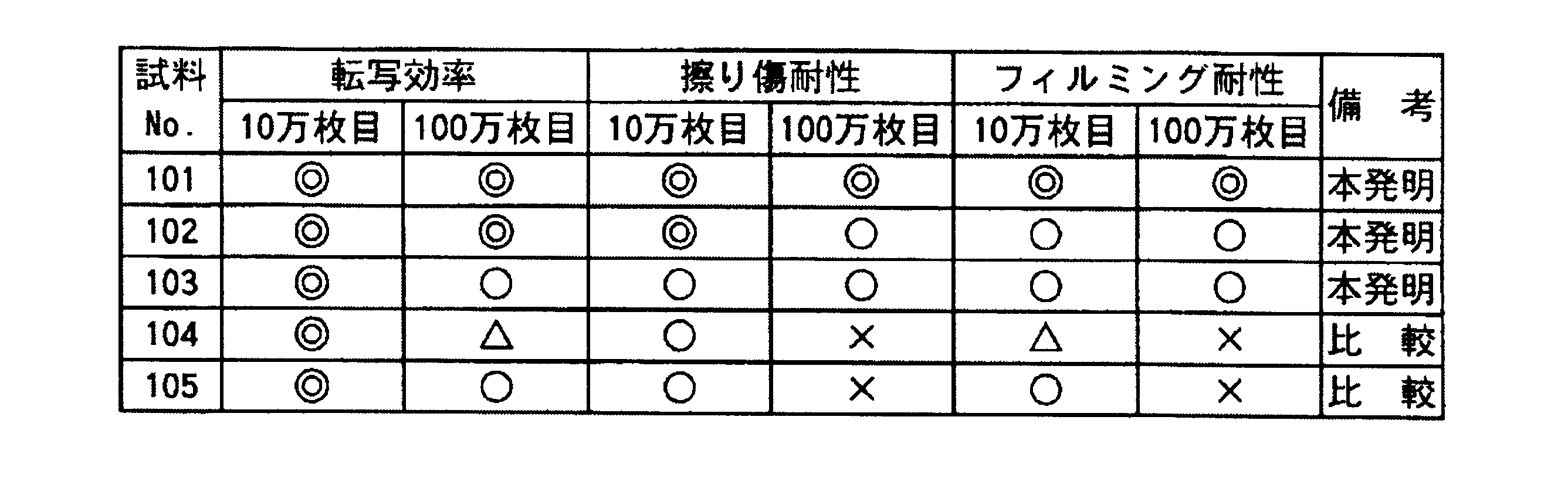
表1(低温低湿(10℃、20%RH)での評価)、表2(高温高湿(30℃、80%RH)での評価)の結果より、大気圧プラズマCVD法により形成された無機化合物を有する薄膜にVUVを照射し改質処理し表面層を形成する本発明の中間転写ベルトの製造方法により製造した試料No.101から103は低温低湿(10℃、20%RH)及び、高温高湿(30℃、80%RH)の環境での転写効率、擦り傷耐性及びフィルミングは優れた性能を示すことを確認した。
無機化合物を有する表面層を持たない他は試料No.102と同じ条件で製造した比較試料No.104では転写効率、擦り傷耐性及びフィルミングが試料No.102に比べ劣る結果を示した。
VUV照射の代わりに波長365nmの紫外線を使用して改質処理を行なった他は試料No.102と同じ条件で製造した比較試料No.105は低温低湿(10℃、20%RH)では、転写効率、擦り傷耐性及びフィルミングは試料No.102と同じ性能を示すが、高温高湿(30℃80%RH)の環境で転写効率、擦り傷耐性及びフィルミングが試料No.101に比べ劣る結果を示した。
また、試料No.101から105において、中間転写ベルト基材としてポリイミド樹脂の代わりポリフェニレンサルファイドを用いて中間転写ベルトを製造した以外は同様にして中間転写ベルトを製造した結果、上記表1及び表2に記載の結果と同じ結果を得た。
また、試料No.101から105において、中間転写ベルト基材としてポリイミド樹脂の代わりポリフェニレンサルファイドを用いて中間転写ベルトを製造した以外は同様にして中間転写ベルトを製造した結果、上記表1及び表2に記載の結果と同じ結果を得た。
実施例2
(基材の作製)
実施例1で作製した基材と同じ基材を作製した。
(基材の作製)
実施例1で作製した基材と同じ基材を作製した。
〔中間転写ベルトの製造〕
準備した基材の上に、図3に示す大気圧プラズマ処理装置を用いて、表3に示す様に無機化合物の種類を変え、無機化合物を有する薄膜(下層(第1層)及び上層(最表層、第2層))を形成し改質し表面層を形成し中間転写ベルトを製造し、試料No.201から205とした。
準備した基材の上に、図3に示す大気圧プラズマ処理装置を用いて、表3に示す様に無機化合物の種類を変え、無機化合物を有する薄膜(下層(第1層)及び上層(最表層、第2層))を形成し改質し表面層を形成し中間転写ベルトを製造し、試料No.201から205とした。

A*:SiOx
B*:SiNy
C*:TiO2
D*:Al2O3
E*:In2O3
B*:SiNy
C*:TiO2
D*:Al2O3
E*:In2O3
試料No.201の製造方法
〔無機化合物を有する薄膜の形成〕
準備した基材の上に、図3に示す大気圧プラズマ処理装置を用いて、無機化合物を有する薄膜(下層(第1層)及び上層(最表層、第2層))を形成した。
〔無機化合物を有する薄膜の形成〕
準備した基材の上に、図3に示す大気圧プラズマ処理装置を用いて、無機化合物を有する薄膜(下層(第1層)及び上層(最表層、第2層))を形成した。
(無機化合物を有する薄膜(下層(第1層))の形成)
下層(第1層)の形成材料としては、下記の下層(第1層)混合ガス組成物を用い、下記の膜形成条件で行った。この時の大気圧プラズマ処理装置の各電極を被覆する誘電体は対向する両電極共に、セラミックス溶射加工により片肉で1mm厚のアルミナを被覆したものを使用した。被覆後の電極間隙は、1mmに設定した。又、誘電体を被覆した金属母材は、冷却水による冷却機能を有するステンレス製ジャケット仕様であり、放電中は冷却水による電極温度コントロールを行いながら実施し、炭素原子含有率5.0原子%、表面硬度2.5GPa、厚さ20nmの下層(第1層)SiOxCyを形成した。炭素原子含有率、表面硬度、厚さは実施例1と同じ方法で測定した値を示す。
下層(第1層)の形成材料としては、下記の下層(第1層)混合ガス組成物を用い、下記の膜形成条件で行った。この時の大気圧プラズマ処理装置の各電極を被覆する誘電体は対向する両電極共に、セラミックス溶射加工により片肉で1mm厚のアルミナを被覆したものを使用した。被覆後の電極間隙は、1mmに設定した。又、誘電体を被覆した金属母材は、冷却水による冷却機能を有するステンレス製ジャケット仕様であり、放電中は冷却水による電極温度コントロールを行いながら実施し、炭素原子含有率5.0原子%、表面硬度2.5GPa、厚さ20nmの下層(第1層)SiOxCyを形成した。炭素原子含有率、表面硬度、厚さは実施例1と同じ方法で測定した値を示す。
下層(第1層)の形成条件
〈下層(第1層)混合ガス組成物〉
放電ガス:窒素ガス 96.93体積%
膜形成(原料)ガス:テトラエトキシシラン 0.07体積%
反応ガス:酸素ガス 3.00体積%
各原料ガスは、加熱することで蒸気を生成し、あらかじめ原料が凝集しないように余熱を行った放電ガス及び反応ガスと混合・希釈した後、放電空間への供給を行った。
〈下層(第1層)混合ガス組成物〉
放電ガス:窒素ガス 96.93体積%
膜形成(原料)ガス:テトラエトキシシラン 0.07体積%
反応ガス:酸素ガス 3.00体積%
各原料ガスは、加熱することで蒸気を生成し、あらかじめ原料が凝集しないように余熱を行った放電ガス及び反応ガスと混合・希釈した後、放電空間への供給を行った。
〈下層(第1層)形成条件〉
第1電極側電源類
応用電機社製高周波電源
周波数 80kHz
出力密度 10W/cm2
第2電極側電源類
パール工業社製高周波電源
周波数 13.56MHz
出力密度 10W/cm2
第1電極側電源類
応用電機社製高周波電源
周波数 80kHz
出力密度 10W/cm2
第2電極側電源類
パール工業社製高周波電源
周波数 13.56MHz
出力密度 10W/cm2
(上層(最表層、第2層)の形成)
次に、上記形成した下層(第1層)の上に、図4に示す大気圧プラズマ処理装置を用いて、上層(最表層、第2層)を形成した。
次に、上記形成した下層(第1層)の上に、図4に示す大気圧プラズマ処理装置を用いて、上層(最表層、第2層)を形成した。
上層(最表層、第2層)の形成材料としては、下記の上層(最表層、第2層)混合ガス組成物を用い、上層(最表層、第2層)の形成は、下記の膜形成条件で行った。この時の大気圧プラズマ処理装置の各電極を被覆する誘電体は対向する両電極共に、セラミックス溶射加工により片肉で1mm厚のアルミナを被覆したものを使用した。被覆後の電極間隙は、1mmに設定した。又誘電体を被覆した金属母材は、冷却水による冷却機能を有するステンレス製ジャケット仕様であり、放電中は冷却水による電極温度コントロールを行いながら実施し、表面硬度4.0GPa、厚さ150nmの上層(最表層、第2層)(SiO2)を形成した。表面硬度、厚さは実施例1と同じ方法で測定した値を示す。
〈上層(最表層、第2層)混合ガス組成物〉
放電ガス:窒素ガス 81.95体積%
膜形成(原料)ガス:テトラエトキシシラン 0.05体積%
反応ガス:酸素ガス 18.00体積%
各原料ガスは、加熱することで蒸気を生成し、予め原料が凝集しないように余熱を行った放電ガス及び反応ガスと混合・希釈した後、放電空間への供給を行った。
放電ガス:窒素ガス 81.95体積%
膜形成(原料)ガス:テトラエトキシシラン 0.05体積%
反応ガス:酸素ガス 18.00体積%
各原料ガスは、加熱することで蒸気を生成し、予め原料が凝集しないように余熱を行った放電ガス及び反応ガスと混合・希釈した後、放電空間への供給を行った。
〈上層(最表層、第2層)形成条件〉
第1電極側電源類
応用電機社製高周波電源
周波数 80kHz
出力密度 10W/cm2
第2電極側電源類
パール工業社製高周波電源
周波数 13.56MHz
出力密度 10W/cm2
第1電極側電源類
応用電機社製高周波電源
周波数 80kHz
出力密度 10W/cm2
第2電極側電源類
パール工業社製高周波電源
周波数 13.56MHz
出力密度 10W/cm2
(VUV照射による改質処理)
実施例1の試料No.101と同じ条件、同じ方法で無機化合物を有する薄膜の改質処理を行い表面層を形成し中間転写ベルトを製造し、試料No.201とした。
実施例1の試料No.101と同じ条件、同じ方法で無機化合物を有する薄膜の改質処理を行い表面層を形成し中間転写ベルトを製造し、試料No.201とした。
試料No.202の製造方法
(基材の作製)
実施例1で作製した基材と同じ基材を作製した。
(基材の作製)
実施例1で作製した基材と同じ基材を作製した。
〔無機化合物を有する薄膜の形成〕
作製した基材上に、図3に示す大気圧プラズマ処理装置を用いて、無機化合物を有する薄膜(下層(第1層)及び上層(最表層、第2層))を形成した。
作製した基材上に、図3に示す大気圧プラズマ処理装置を用いて、無機化合物を有する薄膜(下層(第1層)及び上層(最表層、第2層))を形成した。
(無機化合物を有する薄膜(下層(第1層))の形成)
試料No.201と同じ方法で無機化合物を有する薄膜(下層(第1層)を形成した。
試料No.201と同じ方法で無機化合物を有する薄膜(下層(第1層)を形成した。
(無機化合物を有する薄膜(上層(最表層、第2層)の形成)
次に、上記形成した下層(第1層)の上に、図4に示す大気圧プラズマ処理装置を用いて、上層(最表層、第2層)を形成した。
次に、上記形成した下層(第1層)の上に、図4に示す大気圧プラズマ処理装置を用いて、上層(最表層、第2層)を形成した。
上層(最表層、第2層)の形成材料としては、下記の上層(最表層、第2層)混合ガス組成物を用い、上層(最表層、第2層)の形成は、下記の膜形成条件で行った。この時の大気圧プラズマ処理装置の各電極を被覆する誘電体は対向する両電極共に、セラミックス溶射加工により片肉で1mm厚のアルミナを被覆したものを使用した。被覆後の電極間隙は、1mmに設定した。又誘電体を被覆した金属母材は、冷却水による冷却機能を有するステンレス製ジャケット仕様であり、放電中は冷却水による電極温度コントロールを行いながら実施し、表面硬度11GPa、厚さ150nmの上層(最表層、第2層)(SiNx)を形成した。表面硬度、厚さは実施例1と同じ方法で測定した値を示す。
〈上層(最表層、第2層)混合ガス組成物〉
放電ガス:ヘリウムガス 96.95体積%
膜形成(原料)ガス:テトラメチルシラン 0.05体積%
反応ガス:アンモニアガス 3.00体積%
各原料ガスは、加熱することで蒸気を生成し、予め原料が凝集しないように余熱を行った放電ガス及び反応ガスと混合・希釈した後、放電空間への供給を行った。
放電ガス:ヘリウムガス 96.95体積%
膜形成(原料)ガス:テトラメチルシラン 0.05体積%
反応ガス:アンモニアガス 3.00体積%
各原料ガスは、加熱することで蒸気を生成し、予め原料が凝集しないように余熱を行った放電ガス及び反応ガスと混合・希釈した後、放電空間への供給を行った。
〈上層(最表層、第2層)形成条件〉
第1電極側電源類
パール工業社製高周波電源
周波数: 13.56MHz
出力密度: 10W/cm2
第2電極側電源類
なし
第1電極側電源類
パール工業社製高周波電源
周波数: 13.56MHz
出力密度: 10W/cm2
第2電極側電源類
なし
(VUV照射による改質処理)
実施例1の試料No.101と同じ条件、同じ方法で無機化合物を有する薄膜の改質処理を行い表面層を形成し中間転写ベルトを製造し、試料No.202とした。
実施例1の試料No.101と同じ条件、同じ方法で無機化合物を有する薄膜の改質処理を行い表面層を形成し中間転写ベルトを製造し、試料No.202とした。
試料No.203の製造方法
(基材の作製)
実施例1で作製した基材と同じ基材を作製した。
(基材の作製)
実施例1で作製した基材と同じ基材を作製した。
〔無機化合物を有する薄膜の形成〕
作製した基材上に、図3に示す大気圧プラズマ処理装置を用いて、無機化合物を有する薄膜(下層(第1層)及び上層(最表層、第2層))を形成した。
作製した基材上に、図3に示す大気圧プラズマ処理装置を用いて、無機化合物を有する薄膜(下層(第1層)及び上層(最表層、第2層))を形成した。
(無機化合物を有する薄膜(下層(第1層))の形成)
試料No.201と同じ下層(第1層)を、同じ方法で形成した。
試料No.201と同じ下層(第1層)を、同じ方法で形成した。
(上層(最表層、第2層)の形成)
次に、上記形成した下層(第1層)の上に、図4に示す大気圧プラズマ処理装置を用いて、上層(最表層、第2層)を形成した。
次に、上記形成した下層(第1層)の上に、図4に示す大気圧プラズマ処理装置を用いて、上層(最表層、第2層)を形成した。
上層(最表層、第2層)の形成材料としては、下記の上層(最表層、第2層)混合ガス組成物を用い、上層(最表層、第2層)の形成は、下記の膜形成条件で行った。この時の大気圧プラズマ処理装置の各電極を被覆する誘電体は対向する両電極共に、セラミックス溶射加工により片肉で1mm厚のアルミナを被覆したものを使用した。被覆後の電極間隙は、1mmに設定した。又誘電体を被覆した金属母材は、冷却水による冷却機能を有するステンレス製ジャケット仕様であり、放電中は冷却水による電極温度コントロールを行いながら実施し、表面硬度5.0GPa、厚さ150nmの上層(最表層、第2層)(TiO2)を形成した。表面硬度、厚さは実施例1と同じ方法で測定した値を示す。
〈上層(最表層、第2層)混合ガス組成物〉
放電ガス:ヘリウムガス 95.96体積%
膜形成(原料)ガス:テトライソプロポキシチタン 0.04体積%
反応ガス:酸素ガス 4.00体積%
各原料ガスは、加熱することで蒸気を生成し、あらかじめ原料が凝集しないように余熱を行った放電ガス及び反応ガスと混合・希釈した後、放電空間への供給を行った。
放電ガス:ヘリウムガス 95.96体積%
膜形成(原料)ガス:テトライソプロポキシチタン 0.04体積%
反応ガス:酸素ガス 4.00体積%
各原料ガスは、加熱することで蒸気を生成し、あらかじめ原料が凝集しないように余熱を行った放電ガス及び反応ガスと混合・希釈した後、放電空間への供給を行った。
〈上層(最表層、第2層)形成条件〉
第1電極側電源類
パール工業社製高周波電源
周波数: 60.0MHz
出力密度: 10W/cm2
第2電極側電源類
なし
第1電極側電源類
パール工業社製高周波電源
周波数: 60.0MHz
出力密度: 10W/cm2
第2電極側電源類
なし
(VUV照射による改質処理)
実施例1の試料No.101と同じ条件、同じ方法で無機化合物を有する薄膜の改質処理を行い表面層を形成し、中間転写ベルトを製造し、試料No.203とした。
実施例1の試料No.101と同じ条件、同じ方法で無機化合物を有する薄膜の改質処理を行い表面層を形成し、中間転写ベルトを製造し、試料No.203とした。
試料No.204の製造方法
(基材の作製)
実施例1で作製した基材と同じ基材を作製した。
(基材の作製)
実施例1で作製した基材と同じ基材を作製した。
〔無機化合物を有する薄膜の形成〕
作製した基材上に、図3に示す大気圧プラズマ処理装置を用いて、無機化合物を有する薄膜(下層(第1層)及び上層(最表層、第2層))を形成した。
作製した基材上に、図3に示す大気圧プラズマ処理装置を用いて、無機化合物を有する薄膜(下層(第1層)及び上層(最表層、第2層))を形成した。
(無機化合物を有する薄膜(下層(第1層))の形成)
試料No.201と同じ下層(第1層)を、同じ方法で形成した。
試料No.201と同じ下層(第1層)を、同じ方法で形成した。
(上層(最表層、第2層)の形成)
次に、上記形成した下層(第1層)の上に、図4に示す大気圧プラズマ処理装置を用いて、上層(最表層、第2層)を形成した。
次に、上記形成した下層(第1層)の上に、図4に示す大気圧プラズマ処理装置を用いて、上層(最表層、第2層)を形成した。
上層(最表層、第2層)の形成材料としては、下記の上層(最表層、第2層)混合ガス組成物を用い、上層(最表層、第2層)の形成は、下記の膜形成条件で行った。この時の大気圧プラズマ処理装置の各電極を被覆する誘電体は対向する両電極共に、セラミックス溶射加工により片肉で1mm厚のアルミナを被覆したものを使用した。被覆後の電極間隙は、1mmに設定した。又誘電体を被覆した金属母材は、冷却水による冷却機能を有するステンレス製ジャケット仕様であり、放電中は冷却水による電極温度コントロールを行いながら実施し、表面硬度10Gpa、厚さ150nmの上層(最表層、第2層)(Al2O3)を形成した。表面硬度、厚さは実施例1と同じ方法で測定した値を示す。
〈上層(最表層、第2層)混合ガス組成物〉
放電ガス:アルゴンガス 98.47体積%
膜形成(原料)ガス:アルミニウムs-ブトキシド 0.03体積%
反応ガス:酸素ガス 1.50体積%
各原料ガスは、加熱することで蒸気を生成し、あらかじめ原料が凝集しないように余熱を行った放電ガス及び反応ガスと混合・希釈した後、放電空間への供給を行った。
放電ガス:アルゴンガス 98.47体積%
膜形成(原料)ガス:アルミニウムs-ブトキシド 0.03体積%
反応ガス:酸素ガス 1.50体積%
各原料ガスは、加熱することで蒸気を生成し、あらかじめ原料が凝集しないように余熱を行った放電ガス及び反応ガスと混合・希釈した後、放電空間への供給を行った。
〈上層(最表層、第2層)形成条件〉
第1電極側電源類
パール工業社製高周波電源
周波数: 60.0MHz
出力密度: 10W/cm2
第2電極側電源類
なし
第1電極側電源類
パール工業社製高周波電源
周波数: 60.0MHz
出力密度: 10W/cm2
第2電極側電源類
なし
(VUV照射による改質処理)
実施例1の試料No.101と同じ条件、同じ方法で無機化合物を有する薄膜の改質処理を行い表面層を形成し、中間転写ベルトを製造し、試料No.204とした。
実施例1の試料No.101と同じ条件、同じ方法で無機化合物を有する薄膜の改質処理を行い表面層を形成し、中間転写ベルトを製造し、試料No.204とした。
試料No.205の製造方法
(基材の作製)
実施例1で作製した基材と同じ基材を作製した。
(基材の作製)
実施例1で作製した基材と同じ基材を作製した。
〔無機化合物を有する薄膜の形成〕
作製した基材上に、図3に示す大気圧プラズマ処理装置を用いて、無機化合物を有する薄膜(下層(第1層)及び上層(最表層、第2層))を形成した。
作製した基材上に、図3に示す大気圧プラズマ処理装置を用いて、無機化合物を有する薄膜(下層(第1層)及び上層(最表層、第2層))を形成した。
(無機化合物を有する薄膜(下層(第1層))の形成)
試料No.201と同じ下層(第1層)を、同じ方法で形成した。
試料No.201と同じ下層(第1層)を、同じ方法で形成した。
(上層(最表層、第2層)の形成)
次に、上記形成した下層(第1層)の上に、図4に示す大気圧プラズマ処理装置を用いて、上層(最表層、第2層)を形成した。
次に、上記形成した下層(第1層)の上に、図4に示す大気圧プラズマ処理装置を用いて、上層(最表層、第2層)を形成した。
上層(最表層、第2層)の形成材料としては、下記の上層(最表層、第2層)混合ガス組成物を用い、上層(最表層、第2層)の形成は、下記の膜形成条件で行った。この時の大気圧プラズマ処理装置の各電極を被覆する誘電体は対向する両電極共に、セラミックス溶射加工により片肉で1mm厚のアルミナを被覆したものを使用した。被覆後の電極間隙は、1mmに設定した。又誘電体を被覆した金属母材は、冷却水による冷却機能を有するステンレス製ジャケット仕様であり、放電中は冷却水による電極温度コントロールを行いながら実施し、表面硬度4.0GPa、厚さ150nmの上層(最表層、第2層)(In2O3)を形成した。表面硬度、厚さは実施例1と同じ方法で測定した値を示す。
〈上層(最表層、第2層)混合ガス組成物〉
放電ガス:アルゴンガス 99.45体積%
膜形成(原料)ガス:インジウムアセチルアセトナート 0.05体積%
反応ガス:水素ガス 0.50体積%
各原料ガスは、加熱することで蒸気を生成し、あらかじめ原料が凝集しないように余熱を行った放電ガス及び反応ガスと混合・希釈した後、放電空間への供給を行った。
放電ガス:アルゴンガス 99.45体積%
膜形成(原料)ガス:インジウムアセチルアセトナート 0.05体積%
反応ガス:水素ガス 0.50体積%
各原料ガスは、加熱することで蒸気を生成し、あらかじめ原料が凝集しないように余熱を行った放電ガス及び反応ガスと混合・希釈した後、放電空間への供給を行った。
〈上層(最表層、第2層)形成条件〉
第1電極側電源類
パール工業社製高周波電源
周波数: 60.0MHz
出力密度: 10W/cm2
第2電極側電源類
なし
第1電極側電源類
パール工業社製高周波電源
周波数: 60.0MHz
出力密度: 10W/cm2
第2電極側電源類
なし
(VUV照射による改質処理)
実施例1の試料No.101と同じ条件、同じ方法で無機化合物を有する薄膜の改質処理を行い表面層を形成し、中間転写ベルトを製造し、試料No.205とした。
実施例1の試料No.101と同じ条件、同じ方法で無機化合物を有する薄膜の改質処理を行い表面層を形成し、中間転写ベルトを製造し、試料No.205とした。
評価
製造した試料No.201から205に付き転写効率、擦り傷耐性及びフィルミングを、低温低湿(10℃、20%RH)、高温高湿(30℃、80%RH)で、実施例1と同じ方法で試験し、実施例1と同じ評価ランクに従って評価した低温低湿(10℃、20%RH)環境の結果を表4、高温高湿(30℃、80%RH)環境の結果を表5に示す。
製造した試料No.201から205に付き転写効率、擦り傷耐性及びフィルミングを、低温低湿(10℃、20%RH)、高温高湿(30℃、80%RH)で、実施例1と同じ方法で試験し、実施例1と同じ評価ランクに従って評価した低温低湿(10℃、20%RH)環境の結果を表4、高温高湿(30℃、80%RH)環境の結果を表5に示す。
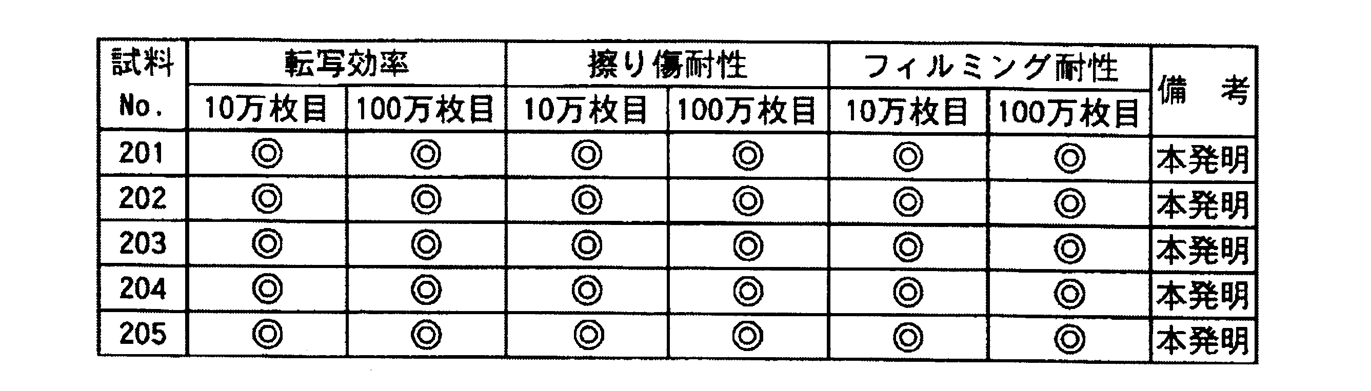

表4(低温低湿(10℃、20%RH)での評価)、表5(高温高湿(30℃、80%RH)での評価)の結果より、表面層を構成する無機化合物の種類を変えて大気圧プラズマCVD法により形成された無機化合物を有する薄膜にVUVを照射し改質処理し表面層を形成する本発明の中間転写ベルトの製造方法により製造した試料No.201から205は低温低湿(10℃、20%RH)及び、高温高湿(30℃、80%RH)の環境での転写効率、擦り傷耐性及びフィルミングは優れた性能を示すことを確認した。
実施例3
(基材の作製)
実施例1で作製した基材と同じ基材を作製した。
(基材の作製)
実施例1で作製した基材と同じ基材を作製した。
(弾性層の作製)
実施例1で作製した弾性層と同じ弾性層を基材の上に実施例1と同じ方法で形成した。
実施例1で作製した弾性層と同じ弾性層を基材の上に実施例1と同じ方法で形成した。
(VUV光源の準備)
表6に示す様に、波長の異なるVUV光源を準備し、No.3-1から3-4とした。
表6に示す様に、波長の異なるVUV光源を準備し、No.3-1から3-4とした。
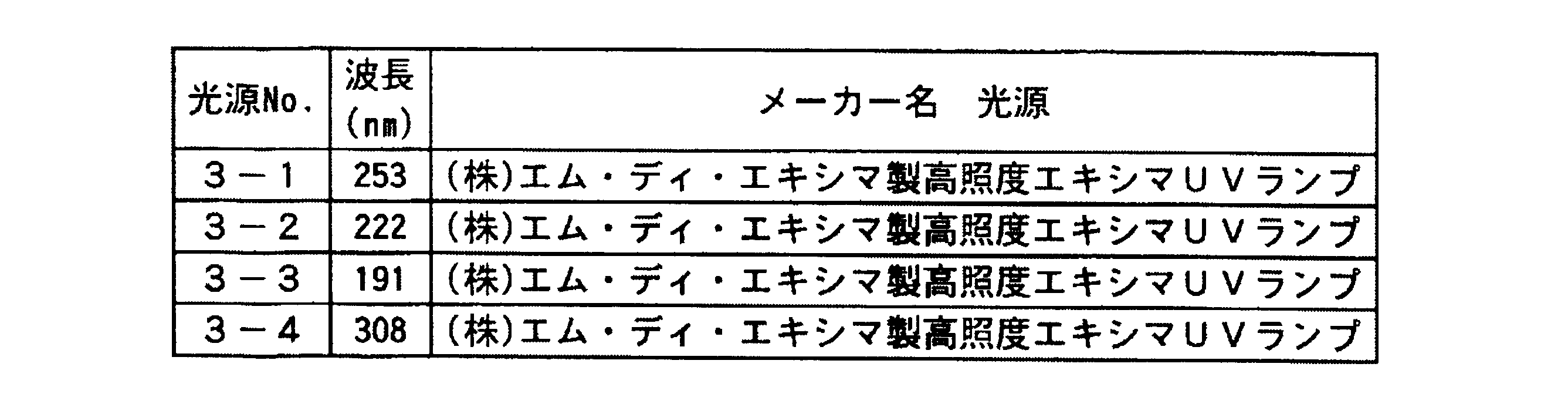
〔無機化合物を有する薄膜の形成〕
上記形成した樹脂層上に、図3に示す大気圧プラズマ処理装置を用いて、実施例1の試料No.101と同じ無機化合物を有する薄膜(下層(第1層)及び上層(最表層、第2層))を、同じ方法で形成した。
上記形成した樹脂層上に、図3に示す大気圧プラズマ処理装置を用いて、実施例1の試料No.101と同じ無機化合物を有する薄膜(下層(第1層)及び上層(最表層、第2層))を、同じ方法で形成した。
(VUV照射による改質処理)
図6に示す改質装置により、準備したVUV光源No.3-1から3-4を使用し、実施例1と同じ条件で形成した無機化合物を有する薄膜にVUVを照射して改質処理を行い表面層を形成し、中間転写ベルトを製造し、試料No.301から304とした。
図6に示す改質装置により、準備したVUV光源No.3-1から3-4を使用し、実施例1と同じ条件で形成した無機化合物を有する薄膜にVUVを照射して改質処理を行い表面層を形成し、中間転写ベルトを製造し、試料No.301から304とした。
評価
製造した試料No.301から304に付き転写効率、擦り傷耐性及びフィルミングを、低温低湿(10℃、20%RH)、高温高湿(30℃、80%RH)で、実施例1と同じ方法で試験し、実施例1と同じ評価ランクに従って評価した低温低湿(10℃、20%RH)環境の結果を表7、高温高湿(30℃、80%RH)環境の結果を表8に示す。
製造した試料No.301から304に付き転写効率、擦り傷耐性及びフィルミングを、低温低湿(10℃、20%RH)、高温高湿(30℃、80%RH)で、実施例1と同じ方法で試験し、実施例1と同じ評価ランクに従って評価した低温低湿(10℃、20%RH)環境の結果を表7、高温高湿(30℃、80%RH)環境の結果を表8に示す。
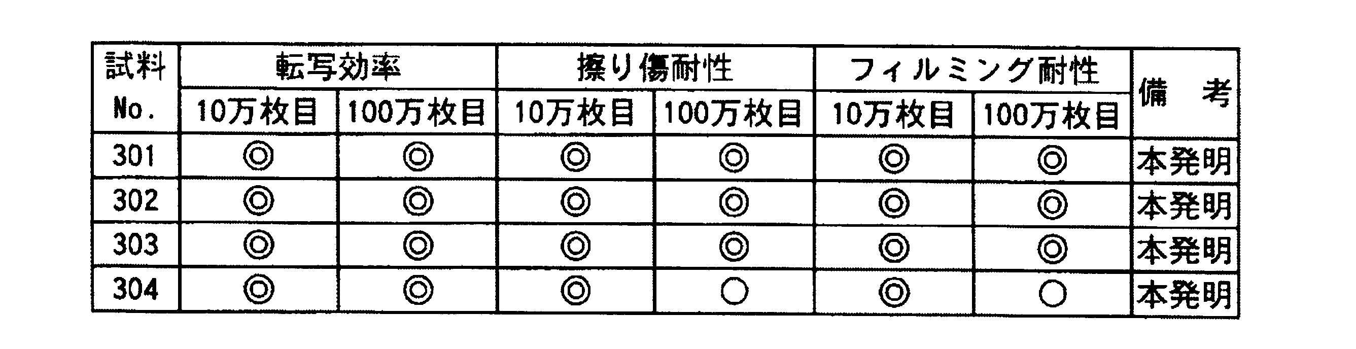
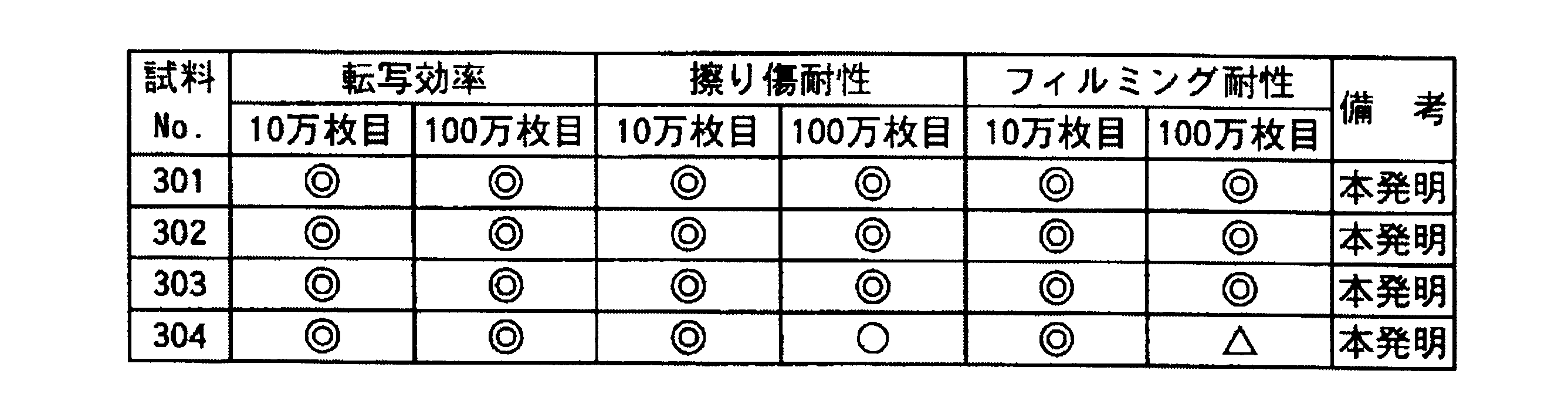
表7(低温低湿(10℃、20%RH)での評価)、表8(高温高湿(30℃、80%RH)での評価)の結果より、大気圧プラズマCVD法により形成された無機化合物を有する薄膜を改質するVUV光源の波長を253nm以下で変えて改質処理を行い表面層を形成し中間転写ベルトを製造した試料No.301から303は低温低湿(10℃、20%RH)及び、高温高湿(30℃、80%RH)の環境での転写効率、擦り傷耐性及びフィルミングは優れた性能を示すことを確認した。
大気圧プラズマCVD法により形成された無機化合物を有する薄膜を改質するVUV光源の波長を308nmで改質処理を行い表面層を形成し中間転写ベルトを製造した試料No.304は低温低湿(10℃、20%RH)及び、高温高湿(30℃、80%RH)の環境での転写効率、擦り傷耐性及びフィルミングは実用上問題とならないが若干劣る性能を示すことを確認した。
以上のように、本発明は、長期間プリントをしても転写効率、擦り傷耐性、フィルミング耐性の低下が発生することなく、高品質の画像を形成することが出来る中間転写ベルトの製造方法に適している。
1 フルカラー画像形成装置
7 無端ベルト状中間転写体形成ユニット
70 中間転写ベルト
70a 基材
70b 弾性層
70c 表面層
3a、3b 大気圧プラズマ処理装置
30 ロール電極
31 固定電極
33、33b 放電空間
34、34b 混合ガス供給装置
35 第1の電源
36 第2の電源
3b1、3b2 大気圧プラズマCVD装置
5 改質装置
501 VUV照射装置
501a VUV光源
501b 改質室
501c 不活性ガス供給口
7 無端ベルト状中間転写体形成ユニット
70 中間転写ベルト
70a 基材
70b 弾性層
70c 表面層
3a、3b 大気圧プラズマ処理装置
30 ロール電極
31 固定電極
33、33b 放電空間
34、34b 混合ガス供給装置
35 第1の電源
36 第2の電源
3b1、3b2 大気圧プラズマCVD装置
5 改質装置
501 VUV照射装置
501a VUV光源
501b 改質室
501c 不活性ガス供給口
Claims (8)
- 基材の上に少なくとも1層の表面層を設けた電子写真方式の画像形成装置に使用する中間転写ベルトの製造方法において、
前記表面層は、無機化合物を有する膜を前記基材の上に設けた後、前記膜に真空紫外光を照射し形成されることを特徴とする中間転写ベルトの製造方法。 - 前記無機化合物を有する膜を大気圧プラズマCVD処理により設けることを特徴とする請求項1に記載の中間転写ベルトの製造方法。
- 前記無機化合物が酸化ケイ素又はSiOαC2-α(α=1.5から2.0)であることを特徴とする請求項1または2に記載の中間転写ベルトの製造方法。
- 前記表面層は、基材上に2層以上設けられることを特徴とする請求項1から3の何れか1項に記載の中間転写ベルトの製造方法。
- 前記2層以上の表面層のうち、前記基材から最も離れて設けられる表面層の炭素含有率が0.1原子数濃度%以下であることを特徴とする請求項4に記載の中間転写ベルトの製造方法。
- 前記真空紫外光を照射する雰囲気の不活性ガス中の酸素濃度が1.0%以下であることを特徴とする請求項1から5の何れか1項に記載の中間転写ベルトの製造方法。
- 前記真空紫外光の波長が、253nm以下であることを特徴とする請求項1から6の何れか1項に記載の中間転写ベルトの製造方法。
- 前記真空紫外光の照射を前記2層以上の表面層の全ての層を設けた後に行うことを特徴とする請求項4から7の何れか1項に記載の中間転写ベルトの製造方法。
Priority Applications (1)
| Application Number | Priority Date | Filing Date | Title |
|---|---|---|---|
| JP2013506006A JP5880543B2 (ja) | 2011-03-24 | 2012-03-22 | 中間転写ベルトの製造方法 |
Applications Claiming Priority (2)
| Application Number | Priority Date | Filing Date | Title |
|---|---|---|---|
| JP2011065436 | 2011-03-24 | ||
| JP2011-065436 | 2011-03-24 |
Publications (1)
| Publication Number | Publication Date |
|---|---|
| WO2012128329A1 true WO2012128329A1 (ja) | 2012-09-27 |
Family
ID=46879470
Family Applications (1)
| Application Number | Title | Priority Date | Filing Date |
|---|---|---|---|
| PCT/JP2012/057383 Ceased WO2012128329A1 (ja) | 2011-03-24 | 2012-03-22 | 中間転写ベルトの製造方法 |
Country Status (2)
| Country | Link |
|---|---|
| JP (1) | JP5880543B2 (ja) |
| WO (1) | WO2012128329A1 (ja) |
Families Citing this family (2)
| Publication number | Priority date | Publication date | Assignee | Title |
|---|---|---|---|---|
| JP5923053B2 (ja) * | 2013-03-28 | 2016-05-24 | 株式会社沖データ | 転写ベルト、転写ベルトユニットおよび画像形成装置 |
| JP6686543B2 (ja) * | 2016-03-04 | 2020-04-22 | 富士ゼロックス株式会社 | 画像形成装置用の弾性ベルト、ベルトユニット、及び画像形成装置 |
Citations (4)
| Publication number | Priority date | Publication date | Assignee | Title |
|---|---|---|---|---|
| JP2006113115A (ja) * | 2004-10-12 | 2006-04-27 | Canon Inc | 弾性部材の表面処理方法 |
| JP2008040139A (ja) * | 2006-08-07 | 2008-02-21 | Shin Etsu Polymer Co Ltd | 無端ベルト及び画像形成装置 |
| JP2010113118A (ja) * | 2008-11-06 | 2010-05-20 | Konica Minolta Business Technologies Inc | 中間転写体 |
| JP2011017858A (ja) * | 2009-07-08 | 2011-01-27 | Yuka Denshi Co Ltd | 画像形成装置用積層ベルト及びその製造方法並びに画像形成装置 |
Family Cites Families (1)
| Publication number | Priority date | Publication date | Assignee | Title |
|---|---|---|---|---|
| CN102356359B (zh) * | 2009-03-18 | 2015-06-17 | 柯尼卡美能达商用科技株式会社 | 中间转印体 |
-
2012
- 2012-03-22 WO PCT/JP2012/057383 patent/WO2012128329A1/ja not_active Ceased
- 2012-03-22 JP JP2013506006A patent/JP5880543B2/ja not_active Expired - Fee Related
Patent Citations (4)
| Publication number | Priority date | Publication date | Assignee | Title |
|---|---|---|---|---|
| JP2006113115A (ja) * | 2004-10-12 | 2006-04-27 | Canon Inc | 弾性部材の表面処理方法 |
| JP2008040139A (ja) * | 2006-08-07 | 2008-02-21 | Shin Etsu Polymer Co Ltd | 無端ベルト及び画像形成装置 |
| JP2010113118A (ja) * | 2008-11-06 | 2010-05-20 | Konica Minolta Business Technologies Inc | 中間転写体 |
| JP2011017858A (ja) * | 2009-07-08 | 2011-01-27 | Yuka Denshi Co Ltd | 画像形成装置用積層ベルト及びその製造方法並びに画像形成装置 |
Also Published As
| Publication number | Publication date |
|---|---|
| JPWO2012128329A1 (ja) | 2014-07-24 |
| JP5880543B2 (ja) | 2016-03-09 |
Similar Documents
| Publication | Publication Date | Title |
|---|---|---|
| CN102356359B (zh) | 中间转印体 | |
| US8802336B2 (en) | Intermediate transfer member comprising an inorganic layer, and image forming method and image forming apparatus employing thereof | |
| US7773927B2 (en) | Intermediate transfer member, method of manufacturing intermediate transfer member, and image forming apparatus | |
| JPWO2008146743A1 (ja) | 中間転写体 | |
| US20110206422A1 (en) | Intermediate transfer member | |
| CN101617276B (zh) | 中间转印体以及图像形成装置 | |
| CN102349029B (zh) | 中间转印体 | |
| JP5282297B2 (ja) | 中間転写体 | |
| JP2010113118A (ja) | 中間転写体 | |
| JP5880543B2 (ja) | 中間転写ベルトの製造方法 | |
| CN101292199B (zh) | 中间转印体、中间转印体的制造方法以及具有中间转印体的图像形成装置 | |
| JP5545051B2 (ja) | 中間転写体 | |
| JP4497205B2 (ja) | 中間転写体、中間転写体の製造方法及び画像形成装置 | |
| JP5262723B2 (ja) | 大気圧プラズマ処理装置及び大気圧プラズマ処理方法 | |
| JPWO2008084714A1 (ja) | 中間転写体、それを用いた画像形成方法及び画像形成装置 | |
| JP2008256958A (ja) | 中間転写体、該中間転写体の製造方法、該中間転写体を用いる画像形成方法及び画像形成装置 | |
| JP2010039253A (ja) | 中間転写体、画像形成装置 |
Legal Events
| Date | Code | Title | Description |
|---|---|---|---|
| 121 | Ep: the epo has been informed by wipo that ep was designated in this application |
Ref document number: 12761108 Country of ref document: EP Kind code of ref document: A1 |
|
| ENP | Entry into the national phase |
Ref document number: 2013506006 Country of ref document: JP Kind code of ref document: A |
|
| NENP | Non-entry into the national phase |
Ref country code: DE |
|
| 122 | Ep: pct application non-entry in european phase |
Ref document number: 12761108 Country of ref document: EP Kind code of ref document: A1 |