WO2012127901A1 - 荷電粒子線装置及びパターン測定方法 - Google Patents
荷電粒子線装置及びパターン測定方法 Download PDFInfo
- Publication number
- WO2012127901A1 WO2012127901A1 PCT/JP2012/051812 JP2012051812W WO2012127901A1 WO 2012127901 A1 WO2012127901 A1 WO 2012127901A1 JP 2012051812 W JP2012051812 W JP 2012051812W WO 2012127901 A1 WO2012127901 A1 WO 2012127901A1
- Authority
- WO
- WIPO (PCT)
- Prior art keywords
- signal
- charged particle
- ratio
- particle beam
- filter
- Prior art date
- Legal status (The legal status is an assumption and is not a legal conclusion. Google has not performed a legal analysis and makes no representation as to the accuracy of the status listed.)
- Ceased
Links
Images











Classifications
-
- H—ELECTRICITY
- H01—ELECTRIC ELEMENTS
- H01J—ELECTRIC DISCHARGE TUBES OR DISCHARGE LAMPS
- H01J37/00—Discharge tubes with provision for introducing objects or material to be exposed to the discharge, e.g. for the purpose of examination or processing thereof
- H01J37/02—Details
- H01J37/04—Arrangements of electrodes and associated parts for generating or controlling the discharge, e.g. electron-optical arrangement or ion-optical arrangement
- H01J37/05—Electron or ion-optical arrangements for separating electrons or ions according to their energy or mass
-
- H—ELECTRICITY
- H01—ELECTRIC ELEMENTS
- H01J—ELECTRIC DISCHARGE TUBES OR DISCHARGE LAMPS
- H01J37/00—Discharge tubes with provision for introducing objects or material to be exposed to the discharge, e.g. for the purpose of examination or processing thereof
- H01J37/02—Details
- H01J37/244—Detectors; Associated components or circuits therefor
-
- G—PHYSICS
- G01—MEASURING; TESTING
- G01N—INVESTIGATING OR ANALYSING MATERIALS BY DETERMINING THEIR CHEMICAL OR PHYSICAL PROPERTIES
- G01N23/00—Investigating or analysing materials by the use of wave or particle radiation, e.g. X-rays or neutrons, not covered by groups G01N3/00 – G01N17/00, G01N21/00 or G01N22/00
- G01N23/22—Investigating or analysing materials by the use of wave or particle radiation, e.g. X-rays or neutrons, not covered by groups G01N3/00 – G01N17/00, G01N21/00 or G01N22/00 by measuring secondary emission from the material
- G01N23/225—Investigating or analysing materials by the use of wave or particle radiation, e.g. X-rays or neutrons, not covered by groups G01N3/00 – G01N17/00, G01N21/00 or G01N22/00 by measuring secondary emission from the material using electron or ion
- G01N23/2251—Investigating or analysing materials by the use of wave or particle radiation, e.g. X-rays or neutrons, not covered by groups G01N3/00 – G01N17/00, G01N21/00 or G01N22/00 by measuring secondary emission from the material using electron or ion using incident electron beams, e.g. scanning electron microscopy [SEM]
-
- G—PHYSICS
- G06—COMPUTING OR CALCULATING; COUNTING
- G06T—IMAGE DATA PROCESSING OR GENERATION, IN GENERAL
- G06T1/00—General purpose image data processing
-
- H—ELECTRICITY
- H01—ELECTRIC ELEMENTS
- H01J—ELECTRIC DISCHARGE TUBES OR DISCHARGE LAMPS
- H01J37/00—Discharge tubes with provision for introducing objects or material to be exposed to the discharge, e.g. for the purpose of examination or processing thereof
- H01J37/26—Electron or ion microscopes; Electron or ion diffraction tubes
- H01J37/28—Electron or ion microscopes; Electron or ion diffraction tubes with scanning beams
-
- H—ELECTRICITY
- H01—ELECTRIC ELEMENTS
- H01J—ELECTRIC DISCHARGE TUBES OR DISCHARGE LAMPS
- H01J2237/00—Discharge tubes exposing object to beam, e.g. for analysis treatment, etching, imaging
- H01J2237/244—Detection characterized by the detecting means
- H01J2237/24475—Scattered electron detectors
-
- H—ELECTRICITY
- H01—ELECTRIC ELEMENTS
- H01J—ELECTRIC DISCHARGE TUBES OR DISCHARGE LAMPS
- H01J2237/00—Discharge tubes exposing object to beam, e.g. for analysis treatment, etching, imaging
- H01J2237/244—Detection characterized by the detecting means
- H01J2237/24485—Energy spectrometers
-
- H—ELECTRICITY
- H01—ELECTRIC ELEMENTS
- H01J—ELECTRIC DISCHARGE TUBES OR DISCHARGE LAMPS
- H01J2237/00—Discharge tubes exposing object to beam, e.g. for analysis treatment, etching, imaging
- H01J2237/244—Detection characterized by the detecting means
- H01J2237/2449—Detector devices with moving charges in electric or magnetic fields
-
- H—ELECTRICITY
- H01—ELECTRIC ELEMENTS
- H01J—ELECTRIC DISCHARGE TUBES OR DISCHARGE LAMPS
- H01J2237/00—Discharge tubes exposing object to beam, e.g. for analysis treatment, etching, imaging
- H01J2237/244—Detection characterized by the detecting means
- H01J2237/24495—Signal processing, e.g. mixing of two or more signals
Definitions
- the present invention relates to a charged particle beam apparatus for generating an image by detecting signal electrons generated from a sample by irradiation of a charged particle beam, and a method for measuring a pattern on a sample surface based on the image.
- SEM scanning electron microscope
- Patent Document 1 discloses mounting of an energy filter that can select signal electrons to be detected on the basis of its energy in an SEM. This type of SEM can obtain a contrast image according to the difference in the surface potential of the device by adjusting the threshold voltage of the energy filter.
- Patent Document 2 discloses an SEM in which a detector for back scattered electrons and a detector for secondary electrons are mounted.
- Patent No. 4069624 Japanese Patent Application Laid-Open No. 8-27369
- the contrast of the backscattered electron image is low. For this reason, it is difficult to measure a pattern based only on a backscattered electron image. Therefore, it is a reasonable judgment to combine the backscattered electron image with the secondary electron image when managing the shape and size.
- Patent Document 2 does not disclose a method for determining an optimal ratio for the synthesis of a backscattered electron image and a secondary electron image. For this reason, it is difficult to mount a function for synthesizing a backscattered electron image and a secondary electron image in a shape management / dimension management apparatus for a semiconductor device that is required to be automated and speeded up.
- the present invention provides a charged particle source for irradiating a sample with a primary charged particle beam and first signal electrons having a first energy among signal charged particles generated from the sample.
- a second detector for detecting second signal electrons having second energy among signal charged particles generated from the sample, signal intensity of the first signal electrons, and second signal electrons
- a first calculation unit that generates a detection image corresponding to each combination ratio, and a ratio of signal intensity corresponding to two predetermined areas of the detection image generated for each combination ratio
- a charged particle beam apparatus is proposed that includes a second calculation unit that calculates the ratio and a third calculation unit that determines a mixture ratio to be used for acquiring a detection image based on a change in the ratio of the signal intensity.
- the present invention passes through a charged particle source that irradiates a sample with a primary charged particle beam, an energy filter that separates signal charged particles according to the magnitude of energy, and the energy filter.
- a detector for detecting signal charged particles a first calculation unit for generating a detection image corresponding to each filter voltage by changing a filter voltage applied to the energy filter, and a predetermined detection image generated for each filter voltage
- a second calculation unit that calculates a ratio of signal intensities corresponding to the two areas, and a third calculation unit that determines a filter voltage to be used for acquiring a detected image based on a change in the ratio of signal strengths.
- Proposed charged particle beam device Proposed charged particle beam device.
- FIG. 4 is a diagram illustrating a structure example of a pattern to be observed in the first embodiment.
- the flowchart which determines the setting conditions of a detection system.
- the figure which shows a condition setting screen (initial screen).
- the figure which shows a condition setting screen (observation screen of a reference image).
- the figure which shows a condition setting screen (area selection screen).
- the figure which shows a condition setting screen (filter setting screen).
- FIG. 10 is a diagram illustrating a structure example of a pattern to be observed in the second embodiment. The figure which shows the example of an image at the time of condition setting execution.
- FIG. 10 is a diagram illustrating a structure example of a pattern to be observed in the second embodiment. The figure which shows the example of an image at the time of condition setting execution.
- FIG 10 is a diagram illustrating a structure example of a pattern to be observed in the third embodiment.
- a scanning electron microscope will be described as an example of a charged particle beam apparatus, but the present invention can also be applied to a focused ion beam (FIB: Focused Ion Beam) microscope.
- FIB Focused Ion Beam
- FIG. 1 shows a first embodiment of a scanning electron microscope.
- an electron beam inspection apparatus used for observing circuit patterns and resist patterns formed on a semiconductor wafer, measuring dimensions, measuring shapes, inspecting, and reviewing defects will be described.
- the electron emission source 101 is attached to the electron microscope barrel 1.
- the electron emission source 101 is controlled by the electron source control unit 201 and emits the primary electron beam 102.
- the primary electron beam 102 is accelerated by an electron source acceleration voltage 202 connected to the electron emission source 101.
- the diameter of the primary electron beam 102 is optimized by one or more focusing lenses 103 and the current limiting diaphragm 104.
- the focusing lens 103 is controlled by the lens control unit 203a.
- the primary electron beam 102 is focused on the surface of the sample 106 by the objective lens 105.
- the objective lens 105 is controlled by the lens control unit 203b.
- a negative voltage (retarding voltage) 204 is applied to the sample 106.
- a negative voltage (retarding voltage) 204 By applying a negative voltage (retarding voltage) 204, a deceleration electric field is generated between the sample 106 and the objective lens 105. Due to the deceleration electric field, the primary electron beam 102 is decelerated immediately before the sample and reaches the surface of the sample 106.
- the irradiation voltage is given by electron source acceleration voltage-retarding voltage.
- the primary electron beam 102 is deflected by the deflector 107 and scans the surface of the sample 106. At that time, signal electrons 108 are generated from the scanning position of the primary electron beam 102.
- the deflector 107 is controlled by the deflection control unit 205.
- the signal electrons 108 include a true secondary electron (TSE: True secondary electron) 108a having a kinetic energy smaller than 50 eV and a backscattered electron (Backscattered electron, BSE) having a kinetic energy higher than 50 eV. It is used in the meaning including 108b.
- TSE true secondary electron
- BSE backscattered electron
- the signal electrons 108 generated from the sample 106 are accelerated by the retarding voltage 204 and enter the energy filter 109.
- the signal electrons 108 that have passed through the energy filter 109 collide with a converting electrode 120 and generate second secondary electrons 130.
- the second secondary electrons 130 are detected by the detector 110a.
- the secondary electrons 131 repelled by the energy filter 109 are detected by the detector 110b.
- a positive voltage is applied to the detectors 110a and 110b, and the secondary electrons 130 and 131 are attracted by the electric field generated by the voltage.
- the detection signals of the detectors 110 a and 110 b are amplified by the amplifiers 206 a and 206 b and input to the synthesis operation unit 207.
- the image that has been subjected to the synthesis calculation in the synthesis calculation unit 207 is displayed on the display unit 208.
- control units 201, 203a, 203b, and 205 are controlled in an integrated manner by the central control unit 209. Control values and adjustment values are stored in the storage device 210.
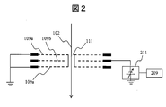
- FIG. 2 shows the basic structure of the energy filter 109.
- the energy filter 109 includes two shield meshes 109a and one filter mesh 109b. These three meshes are provided with openings 111 through which the primary electron beam 102 passes.
- a filter power supply 211 for applying a filter voltage is connected to the filter mesh 109b.
- the filter power supply 211 is controlled by the central control unit 209 as in the other control units.
- one filter mesh 109b is used, but a plurality of filter meshes 109b may be used.
- the plurality of filter meshes 109b may be connected to the filter power supply 211 independently.
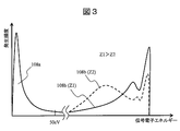
- FIG. 3 schematically shows the energy distribution of signal electrons.
- the horizontal axis is the energy of signal electrons
- the vertical axis is the frequency of occurrence.
- the signal electrons include two types of electrons having different energies and energy. True secondary electrons 108a and backscattered electrons 108b.
- the energy distribution of the true secondary electrons 108a has a peak around several eV to 10 eV.
- the energy distribution of the backscattered electrons 108 b strongly depends on the average atomic number of the sample 106.
- the sample 106 having a large average atomic number (Z1) has an elastic scattering distribution having a peak at an energy substantially equal to the incident energy of the primary electron beam 102.
- the sample 106 having a small average atomic number (Z2) the sample has a peak at about half of the incident energy of the primary electron beam 102.
- the waveform of the backscattered electrons 108b having the smaller energy is indicated by a broken line.
- the energy distribution of signal electrons actually generated during observation varies depending on the material constituting the sample 106. For this reason, the synthesis ratio of the two detection signals output from the two detectors 110a and 110b cannot be determined in advance.
- FIG. 4 shows an example of a surface pattern of a three-dimensional device assumed as a measurement target.
- the upper diagram is a plan view of the three-dimensional device
- the lower diagram is a cross-sectional view of the three-dimensional device.
- metal 301 is embedded in the lowermost layer
- wiring patterns 302 are formed in parallel in a plurality of rows on the upper layer.
- an opening 303 is formed in the base layer in the gap portion between the wiring patterns so as to be electrically connected to the lower layer metal 301.
- FIG. 5 shows a processing procedure executed by the central control unit 209 in accordance with the processing program when setting the detection conditions.
- An example of the setting screen displayed on the display unit 208 at this time is shown in FIG.
- Setting of the detection condition is started by acquiring an initial image (that is, a reference image) of the measurement pattern.
- the central control unit 209 sets the filter voltage to 0 V and the detection signal synthesis ratio to 1: 1.
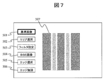
- the screen shown in FIG. Acquisition of the reference image is started when the operator clicks the “reference image” button 501 on the setting screen. After the acquisition operation is completed, the newly acquired reference image (planar image) is displayed on the image display unit 507 of the display unit 208.
- step 402 in order to display the pattern edge to be measured in the image, a screen for accepting selection of an area by the operator is displayed.
- Fig. 8 shows an example of the screen corresponding to this process.
- the operator selects two adjacent areas in the initial image.
- an area selection button 508 is displayed in an area next to the image display unit 507.
- Area boxes 509a and 509b are displayed in a superimposed manner on the reference image of the image display unit 507. These two area boxes are referred to as “area box A” and “area box B”, respectively, in the following description.
- the area selection button 508 is used to select the type of area box set on the reference image.
- the shape used for displaying each area box is selected from the template 510.
- the operator selects the type and shape of the area box and places each area box at an appropriate position on the image.
- the template may be selected after the area box is arranged, and the shape of the area box may be changed.
- the size of the area box may be arbitrarily changed between a preset minimum value and maximum value of the box area.
- the central control unit 209 displays a filter voltage setting screen on the display unit 208 (step 403).
- FIG. 9 shows a filter voltage setting screen.
- the central control unit 209 starts processing for determining an optimum value of the filter voltage.
- the filter voltage setting process can be skipped.
- the central control unit 209 changes the filter voltage step by step by a predetermined amount from the initial value, and acquires an image of the sample 106 each time.
- the central control unit 209 determines whether the filter voltage is changed, each time an image is acquired, the gradation ratio Calculate S A / S B.
- the central control unit 209 optimizes the filter voltage according to the following procedure using the gradation ratio here as an evaluation value.
- FIG. 10-1 shows the relationship between the energy of signal electrons and the signal intensity.
- the horizontal axis is the energy of signal electrons
- the vertical axis is the signal intensity.
- the metal portion (the location selected in the area box A) of the lower layer of the three-dimensional device is composed of heavy metal
- the peripheral portion is composed of light elements.
- the central control unit 209 operates the energy filter 109 to set a finite filter voltage ( ⁇ Vf in the figure). Then, a signal having energy lower than ⁇ Vf is repelled by the energy filter 109, and only a signal having energy higher than ⁇ Vf is detected.
- the detection signal can be prevented from being detected from the [I] part in FIG. At this time, the gradation ratio S A / S B increases.
- ⁇ Vf is too large, the signal intensity from both the signal from area box A and the signal from area box B will be small and cannot be distinguished from noise at the time of signal detection.
- the gradation ratio S is maintained while maintaining the gradation value of the area box A> 5N and the gradation value of the area box B> 5N.
- ⁇ Vf can be determined so as to maximize A / S B.
- the noise threshold is specified to be 5 times or more the noise amplitude N, but this constant may be changed.
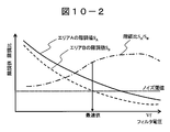
- FIG. 10-2 shows an example in which the gradation ratio S A / S B increases as ⁇ Vf increases.
- S B is smaller than the noise threshold. Therefore, when the gradation ratio S A / S B changes in this way, the central control unit 209 sets ⁇ Vf at which S B becomes equal to the noise threshold value to the optimum value of the filter voltage.
- FIG. 10-3 shows an example in which the gradation ratio S A / S B has a maximum value with respect to ⁇ Vf.
- S A / S B is a maximum. Therefore, the central control unit 209 sets ⁇ Vf when S A / S B is maximized to the optimum value of the filter voltage.
- the central control unit 209 displays an acquired image of the backscattered electron detection image (BSE image) (step 404).
- FIG. 11 shows a BSE image setting screen.
- the central control unit 209 executes BSE image acquisition processing.
- the central control unit 209 uses only the detection signal detected by the detector 110a.
- the central control unit 209 acquires an image using the filter voltage optimized in step 403.
- the central control unit 209 displays the acquired image on the image display unit 507.
- FIG. 12 shows an edge selection screen.
- an edge selection button 505 When the operator presses an “edge selection” button 505 on the setting screen, an edge selection button 511 is displayed in the horizontal area of the image display unit 507.
- An area box 509c is displayed on the BSE image of the image display unit 507.
- the area box for designating the edge is referred to as “area box C” in the following description.
- the shape of the area box is selected from the template 510 by the operator.
- the operator places the area box C at an appropriate position on the BSE image. It is preferable that the size of the area box C can be arbitrarily changed.
- the central control unit 209 displays a setting screen for automatically setting the mixing ratio of the two detection signals on the display unit 208 (step 406).
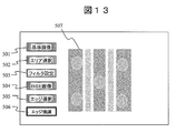
- FIG. 13 shows a mixing ratio setting screen.
- the central control unit 209 starts a process of automatically determining the mixture ratio of the two detectors 110a and 110b.
- the central control unit 209 that has started the processing changes the mixing ratio of the detection signal of the detector 110a and the detection signal of the detector 110b in a stepwise manner, and synthesizes two detection signals each time based on the set mixing ratio. Acquired image.
- the central control unit 209 calculates the gradation ratio S C / S A. Using the gradation ratio as an evaluation value, the central control unit 209 determines an optimal mixing ratio according to the following procedure. However, the area to compare the area box C and the gradation value and area box B, may be calculated gradation ratio S C / S B as an evaluation value.
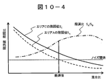
- FIG. 10-4 is an example in which the gradation ratio S C / S A increases as the mixing ratio increases. If the mixing ratio is increased too much, S A becomes smaller than the noise threshold. Therefore, when the gradation ratio S C / S A changes in this way, the central control unit 209 determines the mixing ratio at which S A becomes equal to the noise threshold value as an optimal value.
- Figure 10-5 is an example of the case where the gradation ratio S C / S A has a maximum value with respect to the mixing ratio. In a range of the mixing ratio where both S C and S A do not fall below the noise threshold, S C / S A becomes maximum. Therefore, the central control unit 209 sets the mixing ratio when S C / S A is maximized to an optimum value.
- the central control unit 209 automatically optimizes the mixing ratio of the filter voltage and the detection signal, and acquires an image under the condition that the gradation ratio is the best.
- the optimal mixing ratio for true secondary electrons and backscattered electrons can be automatically set according to the sample 106 to be measured.
- the aperture 303 which is the second darkest in the image and has a small gradation difference from the darkest region.
- the filter voltage for acquiring the reference image is set to 0 V and the detection signal synthesis ratio is set to 1: 1.
- these values may be arbitrarily set by the operator.
- the filter voltage when the filter voltage is determined in step 403, the image of the process is not displayed, but a list of each image when the filter voltage is changed stepwise may be displayed. Further, the operator may look at these list images, and the condition of the arbitrarily selected image may be used as the filter setting voltage.
- the image in the processing process is not displayed, but a list of each image when the composite ratio of the detection signals is changed stepwise. May be displayed. Further, the operator may look at these lists, and an arbitrarily selected image condition may be used as the composition ratio.
- Example 2 14A to 14C, another example of the surface pattern of the three-dimensional device assumed as a measurement target will be described.
- this three-dimensional device a lattice in which a line and space pattern 601 (hereinafter referred to as “lower layer line 601”) extending in the horizontal direction and a line and space 602 (hereinafter referred to as “upper layer line 602”) extending in the vertical direction are stacked.
- lower layer line 601 a line and space pattern 601
- upper layer line 602 hereinafter referred to as “upper layer line 602”
- FIGS. 15A to 15C show examples of images when steps 401 to 406 are executed. As can be seen by comparing FIGS. 15A and 15C, the horizontal streak pattern 1501 that was not displayed in FIG. 15A is drawn in FIG. 15C after adjusting the mixing ratio. Has been.
- the three-dimensional device that can be measured as a measurement target is not limited to the three-dimensional device shown in FIG. 4 or FIG. It is also suitable for measurement of a three-dimensional device having the pattern structure shown in FIGS.
- the three-dimensional device shown in this figure is assumed to have a shape in which the base layer 710 is separated in the arrangement direction of the patterns 711 as shown in FIG. As shown in FIG. 15B, this pattern structure is formed of three layers having different height positions when viewed from the irradiation direction of the primary electron beam. For this reason, a structure in which three representative brightness levels are included in the detection signal is assumed.
- the level difference between the base layer 710 and its base is small. For this reason, the difference in brightness is slight. Therefore, when the reference image is acquired in step 401, the shape of the darkest part 701 needs to be emphasized, and the boundary 702 of the part adjacent to the darkest part needs to be emphasized.
- the method of the present invention can be applied.
- step 403 is a step of emphasizing the shape of the darkest part 701
- step 406 corresponds to a step of emphasizing the contour 702.
- FIG. 17 shows a configuration example of a scanning electron microscope according to another embodiment.
- signal electrons 108 that spread over a wide range from the central axis such as backscattered electrons (BSE) 108b
- BSE backscattered electrons
- annular detector 801a having a large opening with respect to the central axis.
- TSE true secondary electrons
- the signal electrons 108 that are accelerated by the retarding voltage 204 and do not spread over a wide range from the central axis are for passing the primary electron beam 102 in the center.
- Detection is performed by a disk-shaped detector 801b having an opening.
- the detection signals detected by the respective detectors 801a and 801b are amplified by the amplifiers 206a and 206b, and the respective signals are subjected to image calculation by the synthesis calculation unit 207 and then displayed on the display unit 208.
- the detectors 801a and 801b are arranged at different heights in the central axis direction.
- An annular filter mesh 802 having a shape equivalent to that of the detector is disposed under the detection surface of the detector 801a.
- a filter power source 211 is connected to the filter mesh 802, and the filter voltage is controlled by the central control unit 209.
- the technique described in the first embodiment is also applied to a scanning electron microscope having a detector that detects signal electrons that have passed through the energy filter and a detector that detects signal electrons that have not passed through or collided with the energy filter. Can be applied as is.
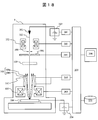
- FIG. 18 illustrates another example of the scanning electron microscope.
- the scanning electron microscope according to the present embodiment uses the energy filter 109 that separates the signal electrons 108 generated from the sample 106 by energy level.
- the detector 901 that detects only secondary electrons that have passed through the energy filter 109 is mounted on the scanning electron microscope.
- the detection signal detected by the detector 901 is amplified by the amplifier 206 and displayed on the display unit 208.
- the energy filter 109 has the configuration shown in FIG.
- the detector 901 is formed in a disk shape having an opening for passing the primary electron beam 102
- the optimum value of the filter power supply 211 for acquiring a backscattered electron (BSE) image due to a difference in material contrast is This can be easily determined by executing steps 401 to 403 shown in FIG.
- Example 4 If two types of signal electrons having different emission angles and energy levels can be separately detected by the two detectors, as shown in FIG. A scanning electron microscope having no filter may be used. In this case, adjustment of the energy filter is unnecessary. Even in this case, the mixing ratio of the two detection signals can be automatically determined by executing the processing from step 404 to step 406 shown in FIG.
- Example 5 In the above-described embodiments, the configuration in which the retarding voltage 204 is applied has been described. However, the retarding voltage 204 may not be applied. Alternatively, a configuration may be employed in which an electrode for applying a positive voltage is disposed immediately above the sample without the retarding voltage 204 being applied, and the signal electrons 108 output from the sample 106 are accelerated. Of course, a configuration may be adopted in which an electrode for applying a positive voltage is applied so that the retarding voltage 204 is applied to pull up and accelerate the signal electrons 108.
- the present invention is not limited to the above-described embodiments, and includes various modifications.
- the above-described embodiments have been described in detail for easy understanding of the present invention, and are not necessarily limited to those having all the configurations described.
- each of the above-described configurations, functions, processing units, processing means, and the like may be partly or entirely realized as, for example, an integrated circuit or other hardware.
- Each of the above-described configurations, functions, and the like may be realized by the processor interpreting and executing a program that realizes each function. That is, it may be realized as software.
- Information such as programs, tables, and files for realizing each function can be stored in a memory, a hard disk, a storage device such as an SSD (Solid State Drive), or a storage medium such as an IC card, an SD card, or a DVD.
- control lines and information lines indicate what is considered necessary for explanation, and do not represent all control lines and information lines necessary for the product. In practice, it can be considered that almost all components are connected to each other.
- Electron microscope tube 101 Electron emission source 102 ... Primary electron beam 103 ... Condensing lens 104 ... Current limiting aperture 105 ... Objective lens 106 ... Sample 107 ... Deflector 108 ... Signal electron 108a ... True secondary electron 108b ... Back scattering Electron 109 ... Energy filter 110a ... Detector 110b ... Detector 120 ... Conversion electrode 130, 131 ... Secondary electron 201 ... Control unit 203a, 203b ... Control unit 205 ... Control unit 204 ... Retarding voltage 206a, 206b ... Amplifier 207 ... Composition calculation unit 208 ... display unit
Landscapes
- Chemical & Material Sciences (AREA)
- Analytical Chemistry (AREA)
- Physics & Mathematics (AREA)
- General Physics & Mathematics (AREA)
- Engineering & Computer Science (AREA)
- Theoretical Computer Science (AREA)
- Health & Medical Sciences (AREA)
- Life Sciences & Earth Sciences (AREA)
- Biochemistry (AREA)
- General Health & Medical Sciences (AREA)
- Immunology (AREA)
- Pathology (AREA)
- Analysing Materials By The Use Of Radiation (AREA)
Abstract
エネルギーの異なる信号荷電粒子の合成機能を自動化することを目的とする。このため、一次荷電粒子線を試料に照射する荷電粒子源と、試料から発生した信号荷電粒子のうち第1のエネルギーを有する第1の信号電子を検出する第1の検出器と、試料から発生した信号荷電粒子のうち第2のエネルギーを有する第2の信号電子を検出する第2の検出器と、第1の信号電子の信号強度と第2の信号電子の信号強度の合成比を変化させ、各合成比に対応する検出画像を生成する第1の演算部と、各合成比について生成された検出画像の所定の2つのエリアに対応する信号強度の比を算出する第2の演算部と、信号強度の比の変化に基づいて、検出画像の取得に使用する混合比を決定する第3の演算部とを荷電粒子線装置に搭載する。
Description
本発明は、荷電粒子線の照射により試料から発生する信号電子を検出して画像を生成する荷電粒子線装置及びその画像に基づいて試料表面のパターンを測定する方法に関する。
半導体デバイスの高集積化に伴い、最表面にあるパターンだけでなく、上層パターンと下層パターンの位置合わせ管理(形状管理)や中層部を貫通するホール開口部の寸法管理が重要となっている。これら多層化されたデバイス(3次元デバイス)の形状管理や寸法管理には、一般に、走査型電子顕微鏡(以下「SEM」という。)が用いられている。
特許文献1は、検出する信号電子を、そのエネルギーにより選別することができるエネルギーフィルタのSEMへの搭載を開示する。この種のSEMは、エネルギーフィルタの閾値電圧を調整することにより、デバイスの表面電位の違いに応じたコントラスト像を得ることができる。
特許文献2は、後方散乱電子(back scattered electron)用の検出器と二次電子(secondary electron)用の検出器を実装するSEMを開示する。
特許文献2は、後方散乱電子(back scattered electron)用の検出器と二次電子(secondary electron)用の検出器を実装するSEMを開示する。
ところが、エネルギーフィルタの閾値電圧(threshold voltage)を、観察デバイスに応じて自動的に設定する方法は知られていない。このため、自動化と高速化が要求される半導体デバイスの形状管理・寸法管理装置には、エネルギーフィルタを実装することが困難である。
また、後方散乱電子像のコントラストは低い。このため、後方散乱電子像だけに基づいてパターンを測定することは困難である。従って、形状管理や寸法管理に際し、後方散乱電子像を二次電子像に合成することは合理的な判断である。
しかし、特許文献2は、後方散乱電子像と二次電子像の合成に最適な比率を決定する手法を開示しない。このため、自動化と高速化が要求される半導体デバイスの形状管理・寸法管理装置への後方散乱電子像と二次電子像の合成機能の搭載は困難である。
本発明は、以上の課題を解決するため、一次荷電粒子線を試料に照射する荷電粒子源と、試料から発生した信号荷電粒子のうち第1のエネルギーを有する第1の信号電子を検出する第1の検出器と、試料から発生した信号荷電粒子のうち第2のエネルギーを有する第2の信号電子を検出する第2の検出器と、第1の信号電子の信号強度と第2の信号電子の信号強度の合成比を変化させ、各合成比に対応する検出画像を生成する第1の演算部と、各合成比について生成された検出画像の所定の2つのエリアに対応する信号強度の比を算出する第2の演算部と、信号強度の比の変化に基づいて、検出画像の取得に使用する混合比を決定する第3の演算部とを有する荷電粒子線装置を提案する。
また、本発明は、以上の課題を解決するため、一次荷電粒子線を試料に照射する荷電粒子源と、信号荷電粒子をエネルギーの大きさに応じて分離するエネルギーフィルタと、エネルギーフィルタを通過した信号荷電粒子を検出する検出器と、エネルギーフィルタに印加するフィルタ電圧を変化させ、各フィルタ電圧に対応する検出画像を生成する第1の演算部と、各フィルタ電圧について生成された検出画像の所定の2つのエリアに対応する信号強度の比を算出する第2の演算部と、信号強度の比の変化に基づいて、検出画像の取得に使用するフィルタ電圧を決定する第3の演算部とを有する荷電粒子線装置を提案する。
本発明によれば、3次元デバイスの形状管理及び寸法管理の自動化に必要な取得条件の設定を自動化できる。上記した以外の課題、構成及び効果は、以下の実施形態の説明により明らかにされる。
以下、図面に基づいて、本発明の実施の形態を説明する。本発明は、後述する形態例に限定されるものでなく、その技術思想の範囲において、種々の変形が可能である。以下の説明では、荷電粒子線装置の一例として走査電子顕微鏡を例に説明するが、本発明は集束イオンビーム(FIB: Focused Ion Beam)顕微鏡にも適用することができる。
<形態例1>
(全体構成)
図1に、走査電子顕微鏡の第1の形態例を示す。ここでは、半導体ウェハ上に形成された回路パターンやレジストパターンの観察、寸法計測、形状計測、検査、欠陥レビューに用いられる電子線検査装置について説明する。
(全体構成)
図1に、走査電子顕微鏡の第1の形態例を示す。ここでは、半導体ウェハ上に形成された回路パターンやレジストパターンの観察、寸法計測、形状計測、検査、欠陥レビューに用いられる電子線検査装置について説明する。
電子顕微鏡鏡筒1には、電子放出源101が取り付けられる。電子放出源101は、電子源制御部201により制御され、一次電子線102を放出する。一次電子線102は、電子放出源101に接続された電子源加速電圧202により加速される。この後、一次電子線102は、一つ以上の集束レンズ103と電流制限絞り104により、その直径が最適化される。集束レンズ103は、レンズ制御部203aにより制御される。その後、一次電子線102は、対物レンズ105により試料106の表面に焦点を結ぶ。対物レンズ105は、レンズ制御部203bにより制御される。
試料106には、負電圧(リターディング電圧)204が印加される。負電圧(リターディング電圧)204の印加により、試料106と対物レンズ105の間には減速電界が発生する。減速電界により、一次電子線102は試料直前で減速され、試料106の表面に到達する。なお、照射電圧は、電子源加速電圧-リターディング電圧で与えられる。
一次電子線102は偏向器107により偏向され、試料106の表面を走査する。その際、一次電子線102の走査位置からは信号電子108が発生される。ここで、偏向器107は、偏向制御部205により制御される。
本形態例の場合、信号電子108は、運動エネルギーが50eVよりも小さい真の二次電子(TSE: True secondary electron)108aと、50eVよりも高い運動エネルギーを持つ後方散乱電子(Backscattered electron,BSE)108bを含む意味で使用する。
試料106から発生した信号電子108は、リターディング電圧204により加速され、エネルギーフィルタ109に入射する。エネルギーフィルタ109を通過した信号電子108は変換電極(converting electrode)120に衝突し、第2の二次電子130を発生する。第2の二次電子130は、検出器110aで検出される。エネルギーフィルタ109で撥ね返された二次電子131は、検出器110bで検出される。なお、検出器110aと110bには正の電圧が印加されており、当該電圧により発生した電界により二次電子130及び131が吸引される。
検出器110a及び110bの検出信号は、増幅器206a及び206bにおいて増幅され、合成演算部207に入力される。合成演算部207において合成演算された後の画像は、表示部208に表示される。
制御部201、203a、203b及び205は、中央制御部209により統合的に制御される。制御値や調整値は記憶装置210に保存される。
図2に、エネルギーフィルタ109の基本構造を示す。エネルギーフィルタ109は、2枚のシールドメッシュ109aと、1枚のフィルタメッシュ109bから構成される。これら3枚のメッシュには、一次電子線102を通過させるための開口111が設けられている。
フィルタメッシュ109bには、フィルタ電圧を印加するためのフィルタ電源211が接続されている。フィルタ電源211は、他の制御部同様、中央制御部209により制御される。図2においては、フィルタメッシュ109bを1枚としているが、複数枚であっても良い。なお、複数枚のフィルタメッシュ109bは、独立にフィルタ電源211に接続される構造でも良い。
(信号電子のエネルギー分布)
図3に、信号電子のエネルギー分布を模式的に示す。ここで、横軸は信号電子のエネルギーであり、縦軸は発生頻度である。前述したように、信号電子には、射出方向とエネルギーが異なる2種類の電子が含まれている。真の二次電子108aと後方散乱電子108bである。
図3に、信号電子のエネルギー分布を模式的に示す。ここで、横軸は信号電子のエネルギーであり、縦軸は発生頻度である。前述したように、信号電子には、射出方向とエネルギーが異なる2種類の電子が含まれている。真の二次電子108aと後方散乱電子108bである。
図3において、真の二次電子108aのエネルギー分布は、数eVから10eVの辺りにピークを持つ。一方、後方散乱電子108bのエネルギー分布は、試料106の平均原子番号に強く依存する。例えば平均原子番号(Z1)が大きい試料106の場合、一次電子線102の入射エネルギーとほぼ等しいエネルギーにピークを持つ弾性散乱的な分布を持つ。一方、平均原子番号(Z2)が小さい試料106の場合、一次電子線102の入射エネルギーの半分程度のエネルギーにピークを持つ。図3においては、エネルギーが小さい方の後方散乱電子108bの波形を破線で示している。
図3に示すように、観察(測定)時に実際に発生する信号電子のエネルギー分布は、試料106を構成する材料により変化する。このため、2つの検出器110a及び110bから出力される2つの検出信号の合成比率を事前に決定することはできない。
以下の実施例では、これら2つの検出信号の合成比率を自動的に調整し、3次元デバイスの形状管理及び寸法管理を自動化する合成演算部207や中央制御部209の処理機能について説明する。
(実施例1)
図4に、測定対象として想定する3次元デバイスの表面パターンの一例を示す。上段の図は3次元デバイスの平面図であり、下段の図は3次元デバイスの断面図である。この3次元デバイスは、最下層に金属301が埋め込まれており、その上層に配線パターン302が複数列平行に形成されている。なお、配線パターン同士のギャップ部分には、下層の金属301と導通させるための開口303が下地層に形成されている。
図4に、測定対象として想定する3次元デバイスの表面パターンの一例を示す。上段の図は3次元デバイスの平面図であり、下段の図は3次元デバイスの断面図である。この3次元デバイスは、最下層に金属301が埋め込まれており、その上層に配線パターン302が複数列平行に形成されている。なお、配線パターン同士のギャップ部分には、下層の金属301と導通させるための開口303が下地層に形成されている。
この3次元デバイスの開口303の寸法を測定する場合、合成画像内におけるギャップ底部と下層の金属部分の区別をはっきりさせる必要がある。
検出条件の設定時に、中央制御部209が、処理プログラムに従って実行する処理手順を図5に示す。この際、表示部208に表示される設定画面の一例を図6に示す。検出条件の設定は、測定パターンの初期画像(すなわち、基準画像)を取得することから開始される。初期画像を取得する際、中央制御部209は、フィルタ電圧を0V、検出信号の合成比率を1:1に設定する。
基準画像の取得時(ステップ401)、表示部208には、図7に示す画面が表示される。基準画像の取得は、オペレータが、設定画面上の「基準画像」ボタン501をクリック操作することで開始される。取得動作の終了後、表示部208の画像表示部507には、新たに取得された基準画像(平面画像)が表示される。
基準画像が取得されると、次は、エリアの入力受付処理に移行する(ステップ402)。ここでは、測定対象とするパターンエッジを画像内に表示させるために、オペレータによるエリアの選択を受け付けるための画面が表示される。
図8に、当該処理に対応する画面例を示す。この画面において、オペレータは、初期画像内で隣接する2つの領域を選択する。オペレータが設定画面内の「エリア選択」ボタン502を押すと、画像表示部507の横の領域に、エリア選択ボタン508が表示される。また、画像表示部507の基準画像の上には、エリアボックス509a及び509bが重畳的に表示される。この二つのエリアボックスを、以下の説明では、それぞれ「エリアボックスA」及び「エリアボックスB」と呼ぶ。
エリア選択ボタン508は、基準画像上に設定するエリアボックスの種類の選択に使用される。各エリアボックスの表示に使用する形状は、テンプレート510の中から選択される。オペレータは、エリアボックスの種類と形状を選択し、画像上の適切な位置に各エリアボックスを配置する。もっとも、エリアボックスの配置後にテンプレートを選択し、エリアボックスの形状を変更しても良い。エリアボックスのサイズは、予め設定されたボックス面積の最小値と最大値の間で任意に変更できるようにすれば良い。
エリアの選択が終了すると、中央制御部209は、フィルタ電圧の設定画面を表示部208に表示する(ステップ403)。図9に、フィルタ電圧の設定画面を示す。オペレータが設定画面の「フィルタ設定」ボタン503を押すと、中央制御部209は、フィルタ電圧の最適値を決定する処理を開始する。なお、後述する検出信号の合成比率に必要な画像が得られている場合には、このフィルタ電圧の設定処理をスキップすることができる。
フィルタ電圧の自動設定処理においては、検出器110aで検出された検出信号だけを使用する。ここで、中央制御部209は、フィルタ電圧を初期値から所定量ずつステップ的に変化させ、その都度、試料106の画像を取得する。画像内のエリアボックスA及びBで囲まれた領域の階調値をそれぞれSA及びSBとすると、中央制御部209は、フィルタ電圧が変更され、画像が取得されるたびに、階調比SA/SBを計算する。中央制御部209は、ここでの階調比を評価値とし、次の手順でフィルタ電圧の最適化を行う。
以下、図10-1~図10-3を用い、フィルタ電圧の最適値を設定する方法を説明する。図10-1に、信号電子のエネルギーと信号強度の関係を示す。横軸は信号電子のエネルギーであり、縦軸は信号強度である。なお、3次元デバイスの下層の金属部分(エリアボックスAで選択した場所)は重金属で構成され、その周辺部(エリアボックスBで選択した場所)は軽元素で構成されることが多い。
その場合、エネルギーが低い二次電子の検出信号の部分では、両者の強度差は僅かである(図中[I]の領域)。一方、エネルギーが入射エネルギーE0に近い後方散乱電子の検出信号の部分では、エリアボックスBの部分よりもエリアボックスAの部分から多く検出される(図中[II]の領域)。
前述したように、中央制御部209は、エネルギーフィルタ109を作動させ、有限のフィルタ電圧(図中ΔVf)を設定する。すると、ΔVfより低いエネルギーの信号は、エネルギーフィルタ109で撥ね返され、ΔVfよりも高エネルギーの信号のみが検出される。
従って、ΔVfを十分大きくすると、図10-1の[I]部からは検出信号を検出しないようにできる。このとき、階調比SA/SBは増大する。一方、ΔVfをあまり大きくしすぎると、エリアボックスAからの信号もエリアボックスBからの信号も信号絶対強度が小さくなり、信号検出時のノイズと区別できなくなってしまう。
ノイズの振幅に相当する画像上の階調をNとし、その5倍をノイズ閾値とすると、エリアボックスAの階調値>5N、エリアボックスBの階調値>5Nを保ちつつ階調比SA/SBを最大化するようにΔVfを決めることが出来る。このとき、ノイズ閾値をノイズ振幅Nの5倍以上と規定したが、この定数は変化しても良い。
ΔVfを最適化する方法を、図10-2及び図10-3を用いて説明する。図10-2は、ΔVfを大きくするほど、階調比SA/SBも大きくなる場合の例を示している。この場合、ΔVfを大きくしすぎると、SBがノイズ閾値より小さくなる。従って、階調比SA/SBがこのように変化する場合、中央制御部209は、SBがノイズ閾値に等しくなるΔVfをフィルタ電圧の最適値に設定する。
図10-3は、階調比SA/SBがΔVfに対して極大値を持つ場合の例である。SA及びSBが共にノイズ閾値を下回らないΔVfの範囲において、SA/SBは極大となる。そこで、中央制御部209は、SA/SBが極大となる時のΔVfをフィルタ電圧の最適値に設定する。
以上の手順は、評価値(階調比SA/SB)を数値化して大小関係を判定するだけであり、自動化することは容易である。中央制御部209は、このようにして求めたフィルタ電圧を最適値に設定する。
フィルタ電圧の設定が終了すると、中央制御部209は、後方散乱電子の検出画像(BSE画像)の取得画像を表示する(ステップ404)。図11に、BSE画像の設定画面を示す。オペレータが「BSE画像」ボタン504を押すと、中央制御部209は、BSE画像の取得処理を実行する。
この場合、中央制御部209は、検出器110aで検出された検出信号だけを使用する。中央制御部209は、ステップ403で最適化されたフィルタ電圧を用いて画像を取得する。中央制御部209は、最適化されたフィルタ電圧に基づいて新たな画像が取得されると、画像表示部507に取得画像を表示する。
BSE画像が取得されると、中央制御部209は、BSE画像内のうち観察しようとするエッジの領域をオペレータに設定入力させるための処理を実行する(ステップ405)。図12に、エッジ選択画面を示す。オペレータが設定画面の「エッジ選択」ボタン505を押すと、画像表示部507の横の領域に、エッジ選択ボタン511が表示される。また、画像表示部507のBSE画像の上には、エリアボックス509cが表示される。このエッジを指定するエリアボックスを、以下の説明では、「エリアボックスC」と呼ぶ。エリアボックスの形状は、オペレータが、テンプレート510から選択する。また、オペレータは、BSE画像上の適切な位置にエリアボックスCを配置する。エリアボックスCのサイズは任意に変更できると良い。
エリアボックスCの設定が終了すると、中央制御部209は、2つの検出信号の混合比を自動設定するための設定画面を表示部208に表示する(ステップ406)。図13に、混合比の設定画面を示す。オペレータが設定画面の「エッジ強調」ボタン506を押すと、中央制御部209は、2つの検出器110a及び110bの混合比を自動的に決定する処理を開始する。
処理を開始した中央制御部209は、検出器110aの検出信号と検出器110bの検出信号の混合比をステップ的に変化させ、その都度、設定された混合比に基づいて2つの検出信号を合成した画像を取得する。
ここで、画像内のエリアボックスCの階調をSCとする。この場合、中央制御部209は、階調比SC/SAを計算する。この階調比を評価値とし、中央制御部209は、以下の手順により最適な混合比を決定する。もっとも、エリアボックスCと階調値を比較する領域をエリアボックスBとし、評価値として階調比SC/SBを算出しても良い。
以下、図10-4及び図10-5を用い、混合比の最適値を設定する方法を説明する。図10-4は、混合比を大きくするほど階調比SC/SAも大きくなる場合の例である。混合比を大きくしすぎると、SAがノイズ閾値より小さくなる。そこで、階調比SC/SAがこのように変化する場合、中央制御部209は、SAがノイズ閾値に等しくなる混合比を最適値に決定する。
これに対し、図10-5は、階調比SC/SAが混合比に対して極大値を持つ場合の例である。SC及びSAが共にノイズ閾値を下回らない混合比の範囲において、SC/SAが極大となる。そこで、中央制御部209は、SC/SAが極大となる時の混合比を最適値に設定する。
(まとめ)
以上の手順により、中央制御部209は、フィルタ電圧と検出信号の混合比を自動的に最適化し、階調比が最も良好となる条件で画像を取得する。これにより、真の二次電子と後方散乱電子に最適な混合比を、測定対象とする試料106に応じて自動的に設定することができる。これにより、画像内で2番目に暗く、最も暗い領域との階調差が小さい開口303の観察が可能になる。これにより、3次元デバイスの構造が未知の場合でも、開口303の寸法を最適な条件で測定することができる。
以上の手順により、中央制御部209は、フィルタ電圧と検出信号の混合比を自動的に最適化し、階調比が最も良好となる条件で画像を取得する。これにより、真の二次電子と後方散乱電子に最適な混合比を、測定対象とする試料106に応じて自動的に設定することができる。これにより、画像内で2番目に暗く、最も暗い領域との階調差が小さい開口303の観察が可能になる。これにより、3次元デバイスの構造が未知の場合でも、開口303の寸法を最適な条件で測定することができる。
なお、前述の実施例においては、基準画像を取得する際のフィルタ電圧を0V、検出信号の合成比率を1:1に設定したが、それらの値はオペレータが任意に設定しても良い。
前述の実施例では、ステップ403でフィルタ電圧を決定する際、処理過程の画像を表示させなかったが、ステップ的にフィルタ電圧を変化させた時の各画像の一覧を表示させても良い。また、これらの一覧画像をオペレータが見て、任意に選択した画像の条件をフィルタ設定電圧としても良い。
前述の実施例では、ステップ406で2つの検出信号の合成比率を決定する際、処理過程の画像を表示させなかったが、ステップ的に検出信号の合成比率を変化させた時の各画像の一覧を表示させも良い。また、これらの一覧表をオペレータが見て、任意に選択した画像の条件を合成比率としても良い。
(実施例2)
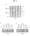
図14(a)~(c)に、測定対象として想定する3次元デバイスの表面パターンの他の一例について説明する。この3次元デバイスにおいては、横方向に延びるライン&スペースパターン601(以下「下層ライン601」という。)と、縦方向に延びるライン&スペース602(以下「上層ライン602」という。)を積層した格子状デバイスを想定する。
図14(a)~(c)に、測定対象として想定する3次元デバイスの表面パターンの他の一例について説明する。この3次元デバイスにおいては、横方向に延びるライン&スペースパターン601(以下「下層ライン601」という。)と、縦方向に延びるライン&スペース602(以下「上層ライン602」という。)を積層した格子状デバイスを想定する。
上層ライン602と下層ライン601が交差する領域を除いた隙間部分603の面積はデバイス特性を左右し、寸法管理が要求される。従って、隙間部分603の横幅を測定する必要があり、下層ライン601と隙間部分603のコントラストを強調しつつ、下層ライン601のエッジと上層ライン602のエッジをそれぞれ明確にする必要がある。
上層ライン601のライン間幅に比べてライン高さが高い場合、ライン間のスペースは深い溝状となり、下層ライン601の有無は判別困難になる。このデバイスにおいても、図5に示した方法によれば、設定パタメータを最適化することができる。図15(a)~(c)に、ステップ401からステップ406まで実行した時の画像例を示す。図15(a)と(c)を比較して分かるように、図15(a)では表示されていなかった横方向の筋模様1501が、混合比を調整した後の図15(c)では描画されている。
(実施例3)
測定対象として測定可能な3次元デバイスは、図4や図14に示す3次元デバイスに限らない。図16(a)~(c)に示すパターン構造を有する3次元デバイスの測定にも好適である。本図に示す3次元デバイスは、図15(b)に示すように、パターン711の並び方向に下地層710が分離されているような形状を想定する。このパターン構造は、図15(b)に示すように、一次電子線の照射方向から見て高さ位置が異なる3つの層で形成される。このため、検出信号には、3つの代表的な明るさが含まれる構造を想定する。
測定対象として測定可能な3次元デバイスは、図4や図14に示す3次元デバイスに限らない。図16(a)~(c)に示すパターン構造を有する3次元デバイスの測定にも好適である。本図に示す3次元デバイスは、図15(b)に示すように、パターン711の並び方向に下地層710が分離されているような形状を想定する。このパターン構造は、図15(b)に示すように、一次電子線の照射方向から見て高さ位置が異なる3つの層で形成される。このため、検出信号には、3つの代表的な明るさが含まれる構造を想定する。
ただし、下地層710とその基体との段差は小さい。このため、その明るさの違いはわずかである。従って、ステップ401における基準画像の取得時には、最も暗い部位701の形状を強調する必要があり、かつ、最も暗い部位と隣り合う部位の境界の輪郭702を強調する必要がある場合には、前述した本発明の方法を適用することができる。
実際、ステップ403は、最も暗い部位701の形状を強調する工程であり、ステップ406は輪郭702を強調する工程に対応する。
<形態例2>
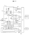
図17に、他の形態例に係る走査電子顕微鏡の構成例を示す。図17には、図1との対応部分に同一符号を付して示す。本形態例の場合、後方散乱電子(BSE)108bのように、中心軸から広範囲に広がった信号電子108は、中心軸に対し大きな開口を有する環状の検出器(annular detector)801aにおいて検出する。また、真の二次電子(TSE)108aのように、リターディング電圧204によって加速され、なおかつ中心軸から広範囲には広がらないような信号電子108は、中心に一次電子線102を通過させるための開口を有する円盤状の検出器801bにおいて検出する。
図17に、他の形態例に係る走査電子顕微鏡の構成例を示す。図17には、図1との対応部分に同一符号を付して示す。本形態例の場合、後方散乱電子(BSE)108bのように、中心軸から広範囲に広がった信号電子108は、中心軸に対し大きな開口を有する環状の検出器(annular detector)801aにおいて検出する。また、真の二次電子(TSE)108aのように、リターディング電圧204によって加速され、なおかつ中心軸から広範囲には広がらないような信号電子108は、中心に一次電子線102を通過させるための開口を有する円盤状の検出器801bにおいて検出する。
それぞれの検出器801a及び801bで検出された検出信号は、増幅器206a及び206bにおいて増幅され、それぞれの信号は、合成演算部207で画像演算された後、表示部208に表示される。
検出器801a及び801bは、それぞれ中心軸方向に高さを変えて配置される。検出器801aの検出面の下には、同検出器と同等の形状を有する環状のフィルタメッシュ802が配置される。フィルタメッシュ802には、フィルタ電源211が接続されており、中央制御部209によりフィルタ電圧が制御される。
このように、エネルギーフィルタを通過した信号電子を検出する検出器と、エネルギーフィルタを通過も衝突もしない信号電子を検出する検出器を有する走査電子顕微鏡の場合にも、形態例1で説明した技術をそのまま応用することができる。
<形態例3>
図18に、走査電子顕微鏡の他の形態例を説明する。本形態例に係る走査電子顕微鏡は、形態例1の場合と同様、試料106から発生した信号電子108をエネルギーレベル別に分離するエネルギーフィルタ109を使用する。
図18に、走査電子顕微鏡の他の形態例を説明する。本形態例に係る走査電子顕微鏡は、形態例1の場合と同様、試料106から発生した信号電子108をエネルギーレベル別に分離するエネルギーフィルタ109を使用する。
ただし、本形態例の場合、エネルギーフィルタ109を通過した二次電子のみを検出する検出器901だけを走査電子顕微鏡に搭載する。この場合、検出器901で検出した検出信号は増幅器206で増幅され、表示部208に表示される。
この形態例の場合、エネルギーフィルタ109は、図2に示す構成を有している。検出器901が、一次電子線102を通すための開口を有する円盤状に形成されている場合、材料コントラストの違いによる後方散乱電子(BSE)像を取得するためのフィルタ電源211の最適値は、図5に示すステップ401からステップ403までを実行すれば容易に決定することができる。
<形態例4>
なお、射出角度とエネルギーレベルが異なる2種類の信号電子を2つの検出器で別々に検出可能であれば、図1との対応部分に同一符号を付して示す図19に示すように、エネルギーフィルタを有しない走査電子顕微鏡であっても良い。この場合において、エネルギーフィルタの調整は不要である。この場合でも、図5に示すステップ404からステップ406までの処理の実行により、2つの検出信号の混合比を自動的に決定することができる。
なお、射出角度とエネルギーレベルが異なる2種類の信号電子を2つの検出器で別々に検出可能であれば、図1との対応部分に同一符号を付して示す図19に示すように、エネルギーフィルタを有しない走査電子顕微鏡であっても良い。この場合において、エネルギーフィルタの調整は不要である。この場合でも、図5に示すステップ404からステップ406までの処理の実行により、2つの検出信号の混合比を自動的に決定することができる。
<形態例5>
前述の形態例においては、いずれもリターディング電圧204を印加する構成について記載した。しかし、リターディング電圧204を印加しなくても良い。また、リターディング電圧204が印加されず、試料直上に正電圧を印加する電極を配置し、試料106から出力された信号電子108を加速的に引上げる構成でも良い。勿論、リターディング電圧204を印加し、信号電子108を引上げ、加速するよう正電圧を印加する電極が配置される構成であっても良い。
前述の形態例においては、いずれもリターディング電圧204を印加する構成について記載した。しかし、リターディング電圧204を印加しなくても良い。また、リターディング電圧204が印加されず、試料直上に正電圧を印加する電極を配置し、試料106から出力された信号電子108を加速的に引上げる構成でも良い。勿論、リターディング電圧204を印加し、信号電子108を引上げ、加速するよう正電圧を印加する電極が配置される構成であっても良い。
<他の形態例>
本発明は上述した形態例に限定されず、様々な変形例を含む。例えば、上述した形態例は、本発明を分かりやすく説明するために詳細に説明したものであり、必ずしも説明した全ての構成を備えるものに限定されるものではない。また、ある形態例の一部を他の形態例の構成に置き換えることが可能であり、また、ある形態例の構成に他の形態例の構成を加えることも可能である。また、各形態例の構成の一部について、他の構成を追加、削除又は置換することも可能である。
本発明は上述した形態例に限定されず、様々な変形例を含む。例えば、上述した形態例は、本発明を分かりやすく説明するために詳細に説明したものであり、必ずしも説明した全ての構成を備えるものに限定されるものではない。また、ある形態例の一部を他の形態例の構成に置き換えることが可能であり、また、ある形態例の構成に他の形態例の構成を加えることも可能である。また、各形態例の構成の一部について、他の構成を追加、削除又は置換することも可能である。
また、上述した各構成、機能、処理部、処理手段等は、それらの一部又は全部を、例えば集積回路その他のハードウェアとして実現しても良い。また、上記の各構成、機能等は、プロセッサがそれぞれの機能を実現するプログラムを解釈し、実行することにより実現しても良い。すなわち、ソフトウェアとして実現しても良い。各機能を実現するプログラム、テーブル、ファイル等の情報は、メモリやハードディスク、SSD(Solid State Drive)等の記憶装置、ICカード、SDカード、DVD等の記憶媒体に格納することができる。
また、制御線や情報線は、説明上必要と考えられるものを示すものであり、製品上必要な全ての制御線や情報線を表すものでない。実際にはほとんど全ての構成が相互に接続されていると考えて良い。
1…電子顕微鏡筒
101…電子放出源
102…一次電子線
103…集束レンズ
104…電流制限絞り
105…対物レンズ
106…試料
107…偏向器
108…信号電子
108a…真の二次電子
108b…後方散乱電子
109…エネルギーフィルタ
110a…検出器
110b…検出器
120…変換電極
130、131…二次電子
201…制御部
203a、203b…制御部
205…制御部
204…リターディング電圧
206a、206b…増幅器
207…合成演算部
208…表示部
101…電子放出源
102…一次電子線
103…集束レンズ
104…電流制限絞り
105…対物レンズ
106…試料
107…偏向器
108…信号電子
108a…真の二次電子
108b…後方散乱電子
109…エネルギーフィルタ
110a…検出器
110b…検出器
120…変換電極
130、131…二次電子
201…制御部
203a、203b…制御部
205…制御部
204…リターディング電圧
206a、206b…増幅器
207…合成演算部
208…表示部
Claims (14)
- 一次荷電粒子線を試料に照射する荷電粒子源と、
前記試料から発生した信号荷電粒子のうち第1のエネルギーを有する第1の信号電子を検出する第1の検出器と、
前記試料から発生した信号荷電粒子のうち第2のエネルギーを有する第2の信号電子を検出する第2の検出器と、
前記第1の信号電子の信号強度と前記第2の信号電子の信号強度の合成比を変化させ、各合成比に対応する検出画像を生成する第1の演算部と、
各合成比について生成された検出画像の所定の2つのエリアに対応する信号強度の比を算出する第2の演算部と、
前記信号強度の比の変化に基づいて、前記検出画像の取得に使用する混合比を決定する第3の演算部と
を有することを特徴とする荷電粒子線装置。 - 請求項1に記載の荷電粒子線装置において、
前記第3の演算部は、前記2つのエリアに対応する2つの信号強度のいずれもが所定の閾値より大きい範囲において、前記信号強度の比の最大値を与える合成比を、前記検出画像の取得時に使用する混合比に決定する
ことを特徴とする荷電粒子線装置。 - 請求項1に記載の荷電粒子線装置において、
前記2つのエリアのうちの一つは、オペレータにより表示画面上で指定されたエッジを指定するエリアである
ことを特徴とする荷電粒子線装置。 - 請求項1に記載の荷電粒子線装置において、
前記第1の検出器と前記第2の検出器で検出される信号荷電粒子をエネルギーの大きさに応じて分離するエネルギーフィルタを有する
ことを特徴とする荷電粒子線装置。 - 請求項4に記載の荷電粒子線装置において、
前記エネルギーフィルタに印加するフィルタ電圧を変化させ、各フィルタ電圧に対応する検出画像を生成する第4の演算部と、
各フィルタ電圧について生成された検出画像の所定の2つのエリアに対応する信号強度の比を算出する第5の演算部と、
前記信号強度の比の変化に基づいて、前記検出画像の取得に使用するフィルタ電圧を決定する第6の演算部と
を有することを特徴とする荷電粒子線装置。 - 請求項5に記載の荷電粒子線装置において、
前記第6の演算部は、前記2つのエリアに対応する2つの信号強度のいずれもが所定の閾値より大きい範囲において、前記信号強度の比の最大値を与えるフィルタ電圧を、前記検出画像の取得時に使用するフィルタ電圧に決定する
ことを特徴とする荷電粒子線装置。 - 請求項5に記載の荷電粒子線装置において、
前記2つのエリアは、オペレータにより表示画面上で指定されたエリアである
ことを特徴とする荷電粒子線装置。 - 請求項4に記載の荷電粒子線装置において、
前記第1の検出器は、前記信号荷電粒子のうち前記エネルギーフィルタを通過した信号荷電粒子により発生される二次電子を検出し、
前記第2の検出器は、前記信号荷電粒子のうち前記エネルギーフィルタに衝突して発生する二次電子を検出する
ことを特徴とする荷電粒子線装置。 - 請求項4に記載の荷電粒子線装置において、
前記第1の検出器は、前記信号荷電粒子のうち前記エネルギーフィルタを通過しない信号荷電粒子を検出し、
前記第2の検出器は、前記信号荷電粒子のうち前記エネルギーフィルタを通過した信号荷電粒子を検出する
ことを特徴とする荷電粒子線装置。 - 一次荷電粒子線を試料に照射する荷電粒子源と、
信号荷電粒子をエネルギーの大きさに応じて分離するエネルギーフィルタと、
前記エネルギーフィルタを通過した信号荷電粒子を検出する検出器と、
前記エネルギーフィルタに印加するフィルタ電圧を変化させ、各フィルタ電圧に対応する検出画像を生成する第1の演算部と、
各フィルタ電圧について生成された検出画像の所定の2つのエリアに対応する信号強度の比を算出する第2の演算部と、
前記信号強度の比の変化に基づいて、前記検出画像の取得に使用するフィルタ電圧を決定する第3の演算部と
を有することを特徴とする荷電粒子線装置。 - 請求項10に記載の荷電粒子線装置において、
前記第3の演算部は、前記2つのエリアに対応する2つの信号強度のいずれもが所定の閾値より大きい範囲において、前記信号強度の比の最大値を与えるフィルタ電圧を、前記検出画像の取得時に使用するフィルタ電圧に決定する
ことを特徴とする荷電粒子線装置。 - 請求項10に記載の荷電粒子線装置において、
前記2つのエリアは、オペレータにより表示画面上で指定されたエリアである
ことを特徴とする荷電粒子線装置。 - 一次荷電粒子線を試料に照射する荷電粒子源と、前記試料から発生した信号荷電粒子のうち第1のエネルギーを有する第1の信号電子を検出する第1の検出器と、前記試料から発生した信号荷電粒子のうち第2のエネルギーを有する第2の信号電子を検出する第2の検出器とを有する荷電粒子線装置におけるパターン測定方法において、
前記第1の信号電子の信号強度と前記第2の信号電子の信号強度の合成比を変化させ、各合成比に対応する検出画像を生成する第1の処理と、
各合成比について生成された検出画像の所定の2つのエリアに対応する信号強度の比を算出する第2の処理と、
前記信号強度の比の変化に基づいて、前記検出画像の取得に使用する混合比を決定する第3の処理と、
決定された混合比を用いて取得された検出画像に基づいてパターンを測定する第4の処理と
を有することを特徴とするパターン測定方法。 - 一次荷電粒子線を試料に照射する荷電粒子源と、信号荷電粒子をエネルギーの大きさに応じて分離するエネルギーフィルタと、前記エネルギーフィルタを通過した信号荷電粒子を検出する検出器とを有する荷電粒子線装置におけるパターン測定方法において、
前記エネルギーフィルタに印加するフィルタ電圧を変化させ、各フィルタ電圧に対応する検出画像を生成する第1の処理と、
各フィルタ電圧について生成された検出画像の所定の2つのエリアに対応する信号強度の比を算出する第2の処理と、
前記信号強度の比の変化に基づいて、前記検出画像の取得に使用するフィルタ電圧を決定する第3の処理と、
決定されたフィルタ電圧を用いて取得された検出画像に基づいてパターンを測定する第4の処理と
を有することを特徴とするパターン測定方法。
Priority Applications (1)
| Application Number | Priority Date | Filing Date | Title |
|---|---|---|---|
| US14/002,275 US8890068B2 (en) | 2011-03-24 | 2012-01-27 | Charged particle ray apparatus and pattern measurement method |
Applications Claiming Priority (2)
| Application Number | Priority Date | Filing Date | Title |
|---|---|---|---|
| JP2011-066724 | 2011-03-24 | ||
| JP2011066724A JP5584159B2 (ja) | 2011-03-24 | 2011-03-24 | 荷電粒子線装置及びパターン測定方法 |
Publications (1)
| Publication Number | Publication Date |
|---|---|
| WO2012127901A1 true WO2012127901A1 (ja) | 2012-09-27 |
Family
ID=46879070
Family Applications (1)
| Application Number | Title | Priority Date | Filing Date |
|---|---|---|---|
| PCT/JP2012/051812 Ceased WO2012127901A1 (ja) | 2011-03-24 | 2012-01-27 | 荷電粒子線装置及びパターン測定方法 |
Country Status (3)
| Country | Link |
|---|---|
| US (1) | US8890068B2 (ja) |
| JP (1) | JP5584159B2 (ja) |
| WO (1) | WO2012127901A1 (ja) |
Cited By (1)
| Publication number | Priority date | Publication date | Assignee | Title |
|---|---|---|---|---|
| CN111937113A (zh) * | 2018-04-06 | 2020-11-13 | 株式会社日立高新技术 | 扫描电子显微镜系统和图案的深度测量方法 |
Families Citing this family (13)
| Publication number | Priority date | Publication date | Assignee | Title |
|---|---|---|---|---|
| JP5663412B2 (ja) * | 2011-06-16 | 2015-02-04 | 株式会社日立ハイテクノロジーズ | 荷電粒子線装置 |
| DE112014000306B4 (de) * | 2013-01-31 | 2020-03-26 | Hitachi High-Technologies Corporation | Kombinierte Ladungsteilchenstrahlvorrichtung |
| JP2017126398A (ja) * | 2014-04-16 | 2017-07-20 | 株式会社日立ハイテクノロジーズ | 荷電粒子線装置 |
| JP2016051593A (ja) * | 2014-08-29 | 2016-04-11 | 株式会社ホロン | リターディング電圧を用いた荷電粒子線装置 |
| JP6565163B2 (ja) * | 2014-10-29 | 2019-08-28 | 株式会社ジェイテクト | 円すいころ軸受 |
| WO2016121009A1 (ja) * | 2015-01-28 | 2016-08-04 | 株式会社 日立ハイテクノロジーズ | 荷電粒子線装置 |
| SG11201707201SA (en) | 2015-03-24 | 2017-10-30 | Kla Tencor Corp | Method and system for charged particle microscopy with improved image beam stabilization and interrogation |
| JP6581940B2 (ja) * | 2016-04-15 | 2019-09-25 | 株式会社日立ハイテクノロジーズ | 電子顕微鏡装置 |
| US10714306B2 (en) * | 2018-06-11 | 2020-07-14 | Applied Materials Israel Ltd. | Measuring a height profile of a hole formed in non-conductive region |
| JP7062563B2 (ja) | 2018-09-07 | 2022-05-06 | キオクシア株式会社 | 輪郭抽出方法、輪郭抽出装置、及びプログラム |
| JP7091263B2 (ja) * | 2019-01-22 | 2022-06-27 | 株式会社日立ハイテク | 電子顕微鏡及び3次元構造の深さ算出方法 |
| JP2022165649A (ja) * | 2021-04-20 | 2022-11-01 | 株式会社日立ハイテク | 欠陥検査装置、及び欠陥検査方法 |
| KR20230068893A (ko) * | 2021-11-11 | 2023-05-18 | 삼성전자주식회사 | 주사 전자 현미경(Scannig Electron Microscope, 이하 SEM), SEM을 동작시키는 방법 및 이를 이용한 반도체 소자를 제조하는 방법 |
Citations (5)
| Publication number | Priority date | Publication date | Assignee | Title |
|---|---|---|---|---|
| JPH0469624B2 (ja) * | 1983-12-08 | 1992-11-06 | Gen Electric | |
| JP2000048752A (ja) * | 1998-05-27 | 2000-02-18 | Jeol Ltd | 電子ビ―ム検査装置とその調整用試料と調整方法およびコンタクトホ―ルの検査方法 |
| JP2001357808A (ja) * | 2000-06-14 | 2001-12-26 | Hitachi Ltd | 回路パターン検査装置および方法 |
| JP2004014229A (ja) * | 2002-06-05 | 2004-01-15 | Hitachi High-Technologies Corp | 荷電粒子線装置 |
| WO2009125603A1 (ja) * | 2008-04-11 | 2009-10-15 | 株式会社荏原製作所 | 試料観察方法及び装置、並びにそれらを用いた検査方法及び装置 |
Family Cites Families (7)
| Publication number | Priority date | Publication date | Assignee | Title |
|---|---|---|---|---|
| US5644132A (en) | 1994-06-20 | 1997-07-01 | Opan Technologies Ltd. | System for high resolution imaging and measurement of topographic and material features on a specimen |
| DE69504294T2 (de) | 1994-12-19 | 1999-04-08 | Opal Technologies Ltd., Nes Ziona | System zur Hochauflösungsbildgebung und Messung von topographischen Characteristiken und Materialcharakteristiken einer Probe |
| US6667476B2 (en) * | 1998-03-09 | 2003-12-23 | Hitachi, Ltd. | Scanning electron microscope |
| US6426501B1 (en) | 1998-05-27 | 2002-07-30 | Jeol Ltd. | Defect-review SEM, reference sample for adjustment thereof, method for adjustment thereof, and method of inspecting contact holes |
| US6847038B2 (en) | 2002-07-15 | 2005-01-25 | Hitachi, Ltd. | Scanning electron microscope |
| KR100494300B1 (ko) * | 2000-03-31 | 2005-06-10 | 가부시끼가이샤 히다치 세이사꾸쇼 | 주사 전자현미경 |
| JP5280174B2 (ja) * | 2008-12-10 | 2013-09-04 | 日本電子株式会社 | 電子線装置及び電子線装置の動作方法 |
-
2011
- 2011-03-24 JP JP2011066724A patent/JP5584159B2/ja active Active
-
2012
- 2012-01-27 US US14/002,275 patent/US8890068B2/en active Active
- 2012-01-27 WO PCT/JP2012/051812 patent/WO2012127901A1/ja not_active Ceased
Patent Citations (5)
| Publication number | Priority date | Publication date | Assignee | Title |
|---|---|---|---|---|
| JPH0469624B2 (ja) * | 1983-12-08 | 1992-11-06 | Gen Electric | |
| JP2000048752A (ja) * | 1998-05-27 | 2000-02-18 | Jeol Ltd | 電子ビ―ム検査装置とその調整用試料と調整方法およびコンタクトホ―ルの検査方法 |
| JP2001357808A (ja) * | 2000-06-14 | 2001-12-26 | Hitachi Ltd | 回路パターン検査装置および方法 |
| JP2004014229A (ja) * | 2002-06-05 | 2004-01-15 | Hitachi High-Technologies Corp | 荷電粒子線装置 |
| WO2009125603A1 (ja) * | 2008-04-11 | 2009-10-15 | 株式会社荏原製作所 | 試料観察方法及び装置、並びにそれらを用いた検査方法及び装置 |
Cited By (2)
| Publication number | Priority date | Publication date | Assignee | Title |
|---|---|---|---|---|
| CN111937113A (zh) * | 2018-04-06 | 2020-11-13 | 株式会社日立高新技术 | 扫描电子显微镜系统和图案的深度测量方法 |
| CN111937113B (zh) * | 2018-04-06 | 2023-06-23 | 株式会社日立高新技术 | 扫描电子显微镜系统和图案的深度测量方法 |
Also Published As
| Publication number | Publication date |
|---|---|
| JP5584159B2 (ja) | 2014-09-03 |
| US8890068B2 (en) | 2014-11-18 |
| JP2012204108A (ja) | 2012-10-22 |
| US20140001360A1 (en) | 2014-01-02 |
Similar Documents
| Publication | Publication Date | Title |
|---|---|---|
| JP5584159B2 (ja) | 荷電粒子線装置及びパターン測定方法 | |
| US11657999B2 (en) | Particle beam system and method for the particle-optical examination of an object | |
| KR101411119B1 (ko) | 하전 입자 빔 현미경 | |
| US8969801B2 (en) | Scanning electron microscope | |
| JP6014688B2 (ja) | 複合荷電粒子線装置 | |
| JP6727024B2 (ja) | 荷電粒子線装置 | |
| JP2013025967A (ja) | 走査透過電子顕微鏡 | |
| US9245711B2 (en) | Charged particle beam apparatus and image forming method | |
| JP7199290B2 (ja) | パターン断面形状推定システム、およびプログラム | |
| JP2020186959A (ja) | パターン評価システム及びパターン評価方法 | |
| US12400383B2 (en) | Training method for learning apparatus, and image generation system | |
| JP2017016755A (ja) | 荷電粒子線装置 | |
| JP2007207688A (ja) | ミラー電子顕微鏡およびミラー電子顕微鏡を用いた検査装置 | |
| WO2013145924A1 (ja) | 走査電子顕微鏡 | |
| US11443914B2 (en) | Charged-particle beam device and cross-sectional shape estimation program | |
| US10192716B2 (en) | Multi-beam dark field imaging | |
| KR102700926B1 (ko) | 하전 입자선 장치 | |
| WO2020136710A1 (ja) | 荷電粒子線装置 | |
| JP5712073B2 (ja) | 試料の検査条件・測定条件の自動判定方法及び走査型顕微鏡 | |
| TWI786618B (zh) | 帶電粒子線裝置 | |
| WO2020225891A1 (ja) | 荷電粒子ビームシステム、および荷電粒子線装置における観察条件を決定する方法 | |
| JP2024164814A (ja) | 分析装置及び分析方法 | |
| McNamara et al. | Modeling Secondary Electron Trajectories in Scanning Electron Microscopes | |
| Miller et al. | Modeling Secondary Electron Trajectories in Scanning Electron Microscopes |
Legal Events
| Date | Code | Title | Description |
|---|---|---|---|
| 121 | Ep: the epo has been informed by wipo that ep was designated in this application |
Ref document number: 12760407 Country of ref document: EP Kind code of ref document: A1 |
|
| WWE | Wipo information: entry into national phase |
Ref document number: 14002275 Country of ref document: US |
|
| NENP | Non-entry into the national phase |
Ref country code: DE |
|
| 122 | Ep: pct application non-entry in european phase |
Ref document number: 12760407 Country of ref document: EP Kind code of ref document: A1 |