WO2012127838A1 - 金属ベース配線板の製造方法及び金属ベース配線板 - Google Patents
金属ベース配線板の製造方法及び金属ベース配線板 Download PDFInfo
- Publication number
- WO2012127838A1 WO2012127838A1 PCT/JP2012/001859 JP2012001859W WO2012127838A1 WO 2012127838 A1 WO2012127838 A1 WO 2012127838A1 JP 2012001859 W JP2012001859 W JP 2012001859W WO 2012127838 A1 WO2012127838 A1 WO 2012127838A1
- Authority
- WO
- WIPO (PCT)
- Prior art keywords
- wiring board
- metal base
- metal
- manufacturing
- insulating material
- Prior art date
- Legal status (The legal status is an assumption and is not a legal conclusion. Google has not performed a legal analysis and makes no representation as to the accuracy of the status listed.)
- Ceased
Links
Images


Classifications
-
- H—ELECTRICITY
- H05—ELECTRIC TECHNIQUES NOT OTHERWISE PROVIDED FOR
- H05K—PRINTED CIRCUITS; CASINGS OR CONSTRUCTIONAL DETAILS OF ELECTRIC APPARATUS; MANUFACTURE OF ASSEMBLAGES OF ELECTRICAL COMPONENTS
- H05K1/00—Printed circuits
- H05K1/02—Details
- H05K1/0201—Thermal arrangements, e.g. for cooling, heating or preventing overheating
- H05K1/0203—Cooling of mounted components
- H05K1/0204—Cooling of mounted components using means for thermal conduction connection in the thickness direction of the substrate
- H05K1/0206—Cooling of mounted components using means for thermal conduction connection in the thickness direction of the substrate by printed thermal vias
-
- H—ELECTRICITY
- H05—ELECTRIC TECHNIQUES NOT OTHERWISE PROVIDED FOR
- H05K—PRINTED CIRCUITS; CASINGS OR CONSTRUCTIONAL DETAILS OF ELECTRIC APPARATUS; MANUFACTURE OF ASSEMBLAGES OF ELECTRICAL COMPONENTS
- H05K3/00—Apparatus or processes for manufacturing printed circuits
- H05K3/0058—Laminating printed circuit boards onto other substrates, e.g. metallic substrates
- H05K3/0061—Laminating printed circuit boards onto other substrates, e.g. metallic substrates onto a metallic substrate, e.g. a heat sink
-
- H—ELECTRICITY
- H05—ELECTRIC TECHNIQUES NOT OTHERWISE PROVIDED FOR
- H05K—PRINTED CIRCUITS; CASINGS OR CONSTRUCTIONAL DETAILS OF ELECTRIC APPARATUS; MANUFACTURE OF ASSEMBLAGES OF ELECTRICAL COMPONENTS
- H05K2201/00—Indexing scheme relating to printed circuits covered by H05K1/00
- H05K2201/02—Fillers; Particles; Fibers; Reinforcement materials
- H05K2201/0203—Fillers and particles
- H05K2201/0206—Materials
- H05K2201/0209—Inorganic, non-metallic particles
-
- H—ELECTRICITY
- H05—ELECTRIC TECHNIQUES NOT OTHERWISE PROVIDED FOR
- H05K—PRINTED CIRCUITS; CASINGS OR CONSTRUCTIONAL DETAILS OF ELECTRIC APPARATUS; MANUFACTURE OF ASSEMBLAGES OF ELECTRICAL COMPONENTS
- H05K2201/00—Indexing scheme relating to printed circuits covered by H05K1/00
- H05K2201/09—Shape and layout
- H05K2201/09209—Shape and layout details of conductors
- H05K2201/095—Conductive through-holes or vias
- H05K2201/0959—Plated through-holes or plated blind vias filled with insulating material
-
- H—ELECTRICITY
- H05—ELECTRIC TECHNIQUES NOT OTHERWISE PROVIDED FOR
- H05K—PRINTED CIRCUITS; CASINGS OR CONSTRUCTIONAL DETAILS OF ELECTRIC APPARATUS; MANUFACTURE OF ASSEMBLAGES OF ELECTRICAL COMPONENTS
- H05K2201/00—Indexing scheme relating to printed circuits covered by H05K1/00
- H05K2201/10—Details of components or other objects attached to or integrated in a printed circuit board
- H05K2201/10007—Types of components
- H05K2201/10166—Transistor
-
- H—ELECTRICITY
- H05—ELECTRIC TECHNIQUES NOT OTHERWISE PROVIDED FOR
- H05K—PRINTED CIRCUITS; CASINGS OR CONSTRUCTIONAL DETAILS OF ELECTRIC APPARATUS; MANUFACTURE OF ASSEMBLAGES OF ELECTRICAL COMPONENTS
- H05K2203/00—Indexing scheme relating to apparatus or processes for manufacturing printed circuits covered by H05K3/00
- H05K2203/06—Lamination
- H05K2203/068—Features of the lamination press or of the lamination process, e.g. using special separator sheets
Definitions
- the present invention relates to a method for manufacturing a metal base wiring board on which a power element is mounted and a metal base wiring board.
- Patent Document 1 discloses a circuit in which a through hole for heat conduction is formed, and resin is filled in the through hole by lamination of a pre-preg, and heat dissipation is improved through the through hole. A substrate is shown.
- Patent Document 2 describes a method in which a through hole is laminated with a pre-preg sandwiched between processed materials, and the through hole is filled with a resin.
- the problem to be solved is that when the heat dissipation is improved by filling the resin into the through hole, the entire through hole cannot be filled with resin accurately by entraining air into the through hole. It is a point.
- the present invention provides a circuit board on which a heating part is mounted on the surface with a wiring portion and a through hole in order to accurately fill the entire through hole with resin by suppressing voids.
- a metal base is laminated on the back surface of the substrate through an insulating material having thermal conductivity and viscosity, and the internal pressure in the through hole is increased by heating and pressing between the circuit board, the insulating material, and the metal base.
- the metal base wiring board manufacturing method is characterized in that the insulating material is moved and filled into the through-hole while suppressing, and a circuit board, an insulating layer in which the insulating material is solidified, and a metal base are stacked.
- a metal-based wiring board manufactured by the method for manufacturing a metal-based wiring board comprising a circuit board having wiring portions and through-holes on which heat-generating components are mounted, and a heat-conductive insulating material attached to the circuit board.
- the metal base wiring board is characterized in that the insulating base is filled from the back side to the front side of the circuit board and filled in the entire through hole.
- the method for manufacturing a metal base wiring board according to the present invention has the above-described configuration, it is possible to fill the entire through hole with an insulating material without generating a void in the through hole.
- the metal-based wiring board of the present invention has the above-described configuration, it is possible to sufficiently dissipate heat from the heat-generating component by heat conduction in the through hole and the insulating material in the entire through hole.
- Example 1 It is a schematic sectional drawing which shows the metal base wiring board with which the power element was mounted. (Example) It is a schematic sectional drawing which shows a metal base wiring board. (Example) It is process drawing which shows the manufacturing method of a metal base wiring board. Example 1 It is a chart which shows application conditions, such as a through hole diameter and a filler particle size. Example 1
- the purpose of making it possible to accurately fill the through hole with resin by suppressing voids is to heat and press between the circuit board, insulating material, and metal base laminates. This was realized by moving and filling the insulating material into the through-hole while suppressing an increase in internal pressure in the hole, and laminating a circuit board, an insulating layer solidified with the insulating material, and a metal base.
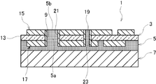
- FIG. 1 is a schematic cross-sectional view showing a metal base wiring board on which a power element is mounted
- FIG. 2 is a schematic cross-sectional view showing the metal base wiring board.
- the metal base wiring board 1 includes a circuit board 3 and a metal base 7 in which the circuit board 3 is laminated with a heat conductive insulating layer 5 interposed therebetween.
- a power element 11 such as a power transistor, which is a heat generating component, is mounted on the hole 9.
- the figure for the sake of simplicity, only one set of the relationship between the through hole 9 and the power element 11 is shown, but actually, a plurality of sets are formed.
- the circuit board 3 is obtained by forming copper foil circuit patterns 15 and 17 as wiring portions on the front surface and the back surface of the substrate 13.
- the substrate 13 is made of, for example, glass or epoxy, and serves as an insulating layer.
- the circuit board 3 is formed with through holes 9 and 19 at predetermined positions. Copper platings 21 and 23 are applied to the inner peripheral surfaces of the through holes 9 and 19 to connect the circuit patterns 15 and 17.
- the diameter of the through hole 9 for heat dissipation including the copper plating 21 should be 0.3 mm or more and the required limit or less.
- “below the necessary limit” is relatively determined by the manufacturing requirements of the circuit board and the mounting requirements of the power element 11, and is 3 mm or less in the embodiment.
- the insulating layer 5 is formed of an insulating material such as an epoxy resin, a silicon resin, an acrylic resin, or an SBS resin, and a part 5a of the insulating material forming the insulating material layer 5 extends from the back side to the front side of the circuit board 3.
- the entire inside of the through hole 9 is filled.
- the exposed surface 5 b of the part 5 a of the insulating material in the through hole 9 is substantially flush with the circuit pattern 15.
- the power element 11 is mounted so as to be in contact with the exposed surface 5 b with respect to the through hole 9.
- the insulating layer 5 and part 5a are mixed with a heat-dissipating filler such as alumina, aluminum nitride, silica, or BN.
- This filler has an average particle size of 25 ⁇ m or less and is relatively determined by the relationship between the insulation withstand voltage characteristic and the heat conduction characteristic of the insulating layer 5 and has a filling rate of 40 to 75% by volume.
- the lower limit of the filler average particle size is, for example, 1 ⁇ m.
- the metal base 7 is made of aluminum or the like.
- the heat generated by the power element 11 is conducted from the exposed surface 5b of the insulating material to the insulating layer 5 through the part 5a, and further conducted to the metal base 7 to be radiated.
- FIG. 3 is a process diagram showing a method of manufacturing a metal base wiring board
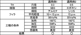
- FIG. 4 is a chart showing implementation conditions such as through-hole diameter and filler particle diameter. 3 are in a semi-finished product state that is not completed as a metal-based wiring board, and the components corresponding to those in FIG.
- FIG. 3 shows a state in which two sets of metal base wiring boards are formed by hot press lamination at a time.
- the metal base 7A, the insulating material 5A, the circuit board (multilayer board) 3A, the sheet 31, the metal base 7A, and the insulation are formed on the hot plate 27 between the upper and lower hot plates 25 and 27 for hot pressing.
- the material 5A, the circuit board (multilayer board) 3A, the sheet 33, and the contact plate 35 are sequentially laminated.
- the sheet 31 used here is a sheet in which a cushion sheet 31a such as a synthetic resin is sandwiched between release papers 31b.
- the diameter of the through hole 9A is set to 0.3 mm or more and the required limit or less, for example, 3 mm or less.
- the resin of the insulating material 5A has a viscosity of 100 kPa ⁇ S or less in a temperature range of 80 to 140 ° C. and a viscosity that can maintain the shape in a free state.
- the insulating material 5A is mixed with a heat-dissipating filler such as alumina, aluminum nitride, silica, or BN.
- the filler has an average particle size of 25 ⁇ m or less and a particle size that can exhibit thermal conductivity, for example, 1 ⁇ m or more, and a filling rate of 40 to 75% by volume.
- the through hole 9A, the insulating material 5A, the filler, and the process conditions in the application example 1 are as follows: the hole diameter of the through hole 9A: 0.3 mm, the resin of the insulating material 5A: SBS, and the filler: alumina. Filler average particle size: 10 to 15 ⁇ m, filler filling rate: 56 Vol%, heating temperature 180 ° C., pressing force: 5 MPa, pressing time: 30 minutes, atmosphere: vacuum.
- the hole diameter of the through hole 9A 0.5 mm
- the resin of the insulating material 5A epoxy
- filler silica
- filler average particle diameter 15 ⁇ m
- filler filling rate 55 vol%
- heating temperature 180 ° C. pressure : 5 MPa
- pressurization time 30 minutes
- atmosphere vacuum.
- the laminate between the circuit board 3A, the insulating material 5A, and the metal base 7A through the sheet 31 is heated and pressurized.
- the insulating material 5A moves from the back side of the circuit board 3A into the through hole 9A by this heating and pressurization.
- the air in the through hole 9A is also released into the vacuum atmosphere through the release paper and the cushion sheet, and the insulating material 5A further moves into the through hole 9A and reaches the surface side of the circuit board 3A. Can do.
- the insulating material 5A is solidified to become the insulating layer 5, and the metal base wiring board 1 in which the circuit board 3, the insulating layer 5 solidified with the insulating material 5A, and the metal base 7 are laminated as shown in FIG. Complete.
- a part 5a of the insulating material forming the insulating material layer 5 extends from the back surface side to the front surface side of the circuit board 3 to fill the entire through hole 9 and solidify. is doing.
- Such filling of the part 5a of the insulating material into the entire through hole 9 could be realized by setting the conditions in FIG. [Effect of Example]
- the metal base 7A is laminated via 5A, and between the lamination of the circuit board 3A, the insulating material 5A, and the metal base 7A is heated and pressurized by the hot plates 25 and 27, and the internal pressure rise of the through hole 9A is increased.
- the insulating material 5A is moved and filled into the through hole 9A while being suppressed by passing air, and the circuit board 3, the insulating layer 5 in which the insulating material 5A is solidified, and the metal base 9 are laminated.
- part of the insulating material 5a can be filled in the entire through hole 9 without generating a void in the through hole 9 of the metal base wiring board 1 completed as shown in FIG.
- the diameter of the through hole 9 was 0.3 mm or more and 3 mm or less.
- the insulating material 5A including a filler having an average particle diameter of 25 ⁇ m or less can smoothly move into the through hole 9 and can be distributed throughout.
- the insulating material 5A has a viscosity of 100 kPa ⁇ S or less in a temperature range of 80 to 140 ° C. and a viscosity capable of maintaining a shape in a free state.
- the insulating material 5A can be smoothly moved into the through hole 9 by heating and pressurization by the upper and lower hot plates 25 and 27, and can be distributed throughout.
- Filler has a filling rate of 40 to 75% by volume.
- the insulating material 5 ⁇ / b> A can be smoothly moved into the through hole 9 and can be distributed throughout.
- Heating and pressurization on the surface side of the circuit board 3A are performed via a sheet 31 that can suppress the increase in internal pressure.
- the insulating material 5A is a resin having a viscosity of 100 kPa ⁇ S or less in a temperature range of 80 to 140 ° C. and having a viscosity that can be held in a free state
- the circuit board 3A, the insulating material 5A, and the metal base Heating and pressurizing between the heat plates 25 and 27 between the laminates via the 7A sheet 31 is an insulating material that has viscosity regardless of the temperature range and solidifies with time after lamination, or solidifies by heating or cooling. If there is, it is also possible to laminate by pressure alone.
Landscapes
- Engineering & Computer Science (AREA)
- Microelectronics & Electronic Packaging (AREA)
- Manufacturing & Machinery (AREA)
- Insulated Metal Substrates For Printed Circuits (AREA)
- Structure Of Printed Boards (AREA)
Abstract
スルー・ホール全体への樹脂の充填を、ボイドを抑制するなどして的確に行わせることを可能とした金属ベース配線板の製造方法及び金属ベース配線板を提供する。 配線部及びスルー・ホール9Aを備え表面にパワー素子を実装する回路基板3Aの裏面に、熱伝導性及び粘性を備えた絶縁材5Aを介して金属ベース7Aを積層し、回路基板3A、絶縁材5A、及び金属ベース7Aの積層間を熱板25,27で加熱・加圧し、スルー・ホール9Aの内圧上昇をシート31を通したエア抜きにより抑制しつつ絶縁材5Aをスルー・ホール9A内へ移動させて充填し、回路基板、前記絶縁材5Aが固化した絶縁層、及び金属ベースを積層形成することを特徴とする。
Description
本発明は、パワー素子が実装される金属ベース配線板の製造方法及び金属ベース配線板に関する。
電気自動車の普及に伴い、パワー・トランジスタ等のパワー素子の需要が増大している。このパワー素子が実装される回路基板では、例えば100A等の大電流に伴う発熱をいかにして放熱するかが課題となる。
この課題に対し、特許文献1には、熱伝導用のスルー・ホールを形成し、このスルー・ホールにプリ・プレグの積層で樹脂を充填し、スルー・ホールを介して放熱性を高めた回路基板が示されている。
しかし、このプリ・プレグによるスルー・ホールへの樹脂の充填は、金属基板の両面にプリ・プレグを積層して行うため、スルー・ホール内に空気を巻き込むことでボイドが発生し易く、放熱性が十分でなくなるという問題があった。
特許文献2には、スルー・ホールを加工された材料間にプリ・プレグを挟んで積層し、スルー・ホールを樹脂で埋める方法が記載されている。
しかし、単にプリ・プレグを挟んで積層しただけでは、スルー・ホール全体を樹脂で的確に埋めることはできないという問題がある。
解決しようとする問題点は、スルー・ホールへの樹脂の充填により放熱性を高める場合に、スルー・ホール内に空気を巻き込むことなどにより、スルー・ホール全体を樹脂で的確に埋めることはできなかった点である。
本発明は、スルー・ホール全体への樹脂の充填を、ボイドを抑制するなどして的確に行わせることを可能とするため、配線部及びスルー・ホールを備え表面に発熱部品を実装する回路基板の裏面に、熱伝導性及び粘性を備えた絶縁材を介して金属ベースを積層し、前記回路基板、絶縁材、及び金属ベースの積層間を加熱・加圧し、前記スルー・ホール内の内圧上昇を抑制しながら前記絶縁材を前記スルー・ホール内へ移動させて充填し、回路基板、前記絶縁材が固化した絶縁層、及び金属ベースを積層形成することを金属ベース配線板の製造方法の特徴とする。
前記金属ベース配線板の製造方法により製造された金属ベース配線板であって、 配線部及びスルー・ホールを備え表面に発熱部品を実装する回路基板と、この回路基板を熱伝導性の絶縁材を介して積層した金属ベースとを備え、前記絶縁材が、前記回路基板の裏面側から表面側に至って前記スルー・ホール内全体に充填されていることを金属ベース配線板の特徴とする。
本発明の金属ベース配線板の製造方法は、上記構成であるから、スルー・ホール内にボイドを発生させることなく絶縁材をスルー・ホール内全体に充填させることができる。
本発明の金属ベース配線板は、上記構成であるから、スルー・ホールおよびスルー・ホール内全体の絶縁材での熱伝導により、発熱部品の放熱を十分に行わせることが可能となる。
スルー・ホール全体への樹脂の充填を、ボイドを抑制するなどして的確に行わせることを可能とするという目的を、回路基板、絶縁材、及び金属ベースの積層間を加熱・加圧し、スルー・ホール内の内圧上昇を抑制しながら前記絶縁材を前記スルー・ホール内へ移動させて充填し、回路基板、前記絶縁材が固化した絶縁層、及び金属ベースを積層形成することにより実現した。
[金属ベース配線板]
図1は、パワー素子が実装された金属ベース配線板を示す概略断面図、図2は、金属ベース配線板を示す概略断面図である。
図1は、パワー素子が実装された金属ベース配線板を示す概略断面図、図2は、金属ベース配線板を示す概略断面図である。
図1、図2のように、金属ベース配線板1は、回路基板3と、この回路基板3を熱伝導性の絶縁層5を介して積層した金属ベース7とを備え、放熱用のスルー・ホール9上に発熱部品であるパワー・トランジスタ等のパワー素子11が実装されている。なお、図では、説明を簡単にするため、スルー・ホール9及びパワー素子11の関係を一組のみ示すが、実際には、複数組形成されている。
回路基板3は、基板13の表面及び裏面に配線部として銅箔の回路パターン15,17が形成されたものである。基板13は、例えば、ガラス・エポキシ等で形成され、絶縁層となっている。回路基板3には、所定箇所にスルー・ホール9,19が形成されている。スルー・ホール9,19の内周面には、銅メッキ21,23が施され、回路パターン15,17を接続している。
放熱用のスルー・ホール9の銅メッキ21を含めた直径は、0.3mm以上必要限度以下とする。この場合の必要限度以下とは、回路基板の製造要件およびパワー素子11の実装要件等により相対的に決定されるものであり、実施例では3mm以下としている。
絶縁層5は、エポキシ樹脂、シリコン樹脂、アクリル樹脂、SBS樹脂等の絶縁材で形成され、絶縁材層5を形成する絶縁材の一部5aが、回路基板3の裏面側から表面側に至ってスルー・ホール9内全体を満たしている。スルー・ホール9内での絶縁材の一部5aは、露出面5bが回路パターン15とほぼ面一となっている。パワー素子11は、スルー・ホール9に対し露出面5bに接するように実装されている。
絶縁層5及び一部5aには、アルミナ、窒化アルミ、シリカ、又はBN等の放熱用のフィラが混在されている。このフィラは、平均粒径25μm以下で絶縁層5の絶縁耐電圧特性と熱伝導特性の関係等により相対的に決定されるものであり、40~75体積%の充填率である。フィラ平均粒径の下限は、例えば、1μmである。
金属ベース7は、アルミ等で形成されている。
したがって、パワー素子11の発熱は、絶縁材の露出面5bから一部5aを介して絶縁層5に伝導し、さらに金属ベース7に伝導して放熱される。
この放熱作用では、絶縁層5及び一部5aでのフィラの混入により高い熱伝導性を持たせることができる。
[金属ベース配線板の製造方法]
図3は、金属ベース配線板の製造方法を示す工程図、図4は、スルー・ホール径とフィラ粒径等の実施条件を示す図表である。なお、図3の各構成部品は、金属ベース配線板として完成していない半製品状態であり、図2と対応する構成部分にAを付して対応を示す。
[金属ベース配線板の製造方法]
図3は、金属ベース配線板の製造方法を示す工程図、図4は、スルー・ホール径とフィラ粒径等の実施条件を示す図表である。なお、図3の各構成部品は、金属ベース配線板として完成していない半製品状態であり、図2と対応する構成部分にAを付して対応を示す。
図3では、2組の金属ベース配線板を一度に熱プレス積層形成する状態を示している。
図3のように、熱プレス用の上下の熱板25,27間で、熱板27上に、金属ベース7A、絶縁材5A、回路基板(多層基板)3A、シート31、金属ベース7A、絶縁材5A、回路基板(多層基板)3A、シート33、当て板35を順次積層配置する。
ここで使用するシート31は、合成樹脂などのクッション・シート31aを離型紙31bで挟んだものである。
スルー・ホール9Aの直径は、上記のように0.3mm以上必要限度以下、例えば3mm以下としている。 絶縁材5Aの樹脂は、80~140℃の温度域で100kPa・S以下で、かつ自由状態で形状保持可能な粘度以上とする。 絶縁材5Aは、アルミナ、窒化アルミ、シリカ、又はBN等の放熱用のフィラを混在させる。
フィラは、平均粒径25μm以下で熱伝導性を発揮し得る粒径以上、例えば1μm以上とし、40~75体積%の充填率とする。
図4のように適用例1でのスルー・ホール9A、絶縁材5A、フィラ、及び工程の条件は、スルー・ホール9Aの穴径:0.3mm、絶縁材5Aの樹脂:SBS、フィラ:アルミナ、フィラ平均粒径:10~15μm、フィラ充填率:56Vol%、加熱温度180℃、加圧力:5MPa、加圧時間:30分、雰囲気:真空とした。
適用例2では、スルー・ホール9Aの穴径:0.5mm、絶縁材5Aの樹脂:エポキシ、フィラ:シリカ、フィラ平均粒径:15μm、フィラ充填率:55Vol%、加熱温度180℃、加圧力:5MPa、加圧時間:30分、雰囲気:真空とした。
次いで、回路基板3A、絶縁材5A、及び金属ベース7Aのシート31を介した積層間を熱板25,27間で加熱・加圧する。
この加熱・加圧により絶縁材5Aが回路基板3Aの裏面側からスルー・ホール9A内へ移動する。
この移動によりスルー・ホール9A内のエアも離型紙およびクッション・シートを通して真空雰囲気中へ逃がされ、絶縁材5Aがスルー・ホール9A内へさらに移動し、回路基板3Aの表面側にまで至ることができる。
その後、冷えると、絶縁材5Aが固化して絶縁層5となり、図2のように回路基板3、前記絶縁材5Aが固化した絶縁層5、及び金属ベース7を積層した金属ベース配線板1が完成する。
図2の金属ベース配線板1では、前記のように絶縁材層5を形成する絶縁材の一部5aが、回路基板3の裏面側から表面側に至ってスルー・ホール9内全体を満たし、固化している。
このような、スルー・ホール9内全体への絶縁材の一部5aの充填は、図4の条件設定により、実現することができた。
[実施例の効果]
本発明の金属ベース配線板1の製造方法では、配線部15,17及びスルー・ホール9Aを備え表面にパワー素子11を実装する回路基板3Aの裏面に、熱伝導性及び粘性を備えた絶縁材5Aを介して金属ベース7Aを積層し、回路基板3A、絶縁材5A、及び金属ベース7Aの積層間を熱板25,27で加熱・加圧し、スルー・ホール9Aの内圧上昇を、シート31を通したエア抜きにより抑制しつつ絶縁材5Aをスルー・ホール9A内へ移動させて充填し、回路基板3、前記絶縁材5Aが固化した絶縁層5、及び金属ベース9を積層形成する。
[実施例の効果]
本発明の金属ベース配線板1の製造方法では、配線部15,17及びスルー・ホール9Aを備え表面にパワー素子11を実装する回路基板3Aの裏面に、熱伝導性及び粘性を備えた絶縁材5Aを介して金属ベース7Aを積層し、回路基板3A、絶縁材5A、及び金属ベース7Aの積層間を熱板25,27で加熱・加圧し、スルー・ホール9Aの内圧上昇を、シート31を通したエア抜きにより抑制しつつ絶縁材5Aをスルー・ホール9A内へ移動させて充填し、回路基板3、前記絶縁材5Aが固化した絶縁層5、及び金属ベース9を積層形成する。
このため、図2のように完成した金属ベース配線板1のスルー・ホール9内にボイドを発生させることなく絶縁材の一部5aをスルー・ホール9内全体に充填させることができる。
スルー・ホール9の直径は、0.3mm以上3mm以下とした。
このため、平均粒径25μm以下のフィラを含む絶縁材5Aがスルー・ホール9内へ円滑に移動し、全体に行き渡らせることができる。
絶縁材5Aは、80~140℃の温度域で100kPa・S以下で、かつ自由状態で形状保持可能な粘度以上である。
このため、上下の熱板25,27による加熱・加圧により絶縁材5Aをスルー・ホール9内へ円滑に移動させ、全体に行き渡らせることができる。
フィラは、40~75体積%の充填率である。
このため、絶縁層5の熱伝導性を十分に高めながら、絶縁材5Aとしてスルー・ホール9内への移動を円滑に行わせ、全体に行き渡らせることができる。
前記回路基板3Aの表面側に対する加熱・加圧は、前記内圧上昇の抑制を可能とするシート31を介して行う。
このため、スルー・ホール9A内のエアは真空雰囲気中へ逃がされスルー・ホール9A内の内圧上昇を抑制することができる。
[その他]
本発明実施例では、絶縁材5Aを、80~140℃の温度域で100kPa・S以下で、かつ自由状態で形状保持可能な粘度以上の樹脂とし、回路基板3A、絶縁材5A、及び金属ベース7Aのシート31を介した積層間を熱板25,27間で加熱・加圧したが、温度域に係わらず粘性を備え、積層後に経時的に固化、或いは加熱又は冷却により固化する絶縁材であれば、加圧のみで積層成形することも可能である。
本発明実施例では、絶縁材5Aを、80~140℃の温度域で100kPa・S以下で、かつ自由状態で形状保持可能な粘度以上の樹脂とし、回路基板3A、絶縁材5A、及び金属ベース7Aのシート31を介した積層間を熱板25,27間で加熱・加圧したが、温度域に係わらず粘性を備え、積層後に経時的に固化、或いは加熱又は冷却により固化する絶縁材であれば、加圧のみで積層成形することも可能である。
1 金属ベース配線板
3,3A 回路基板
5 絶縁層
5A 絶縁材
7,7A 金属ベース
9,9A スルー・ホール
25,27 熱板
31 シート
3,3A 回路基板
5 絶縁層
5A 絶縁材
7,7A 金属ベース
9,9A スルー・ホール
25,27 熱板
31 シート
Claims (9)
- 配線部及びスルー・ホールを備え表面に発熱部品を実装する回路基板の裏面に、熱伝導性及び粘性を備えた絶縁材を介して金属ベースを積層し、
前記回路基板、絶縁材、及び金属ベースの積層間を加圧し、
前記スルー・ホール内の内圧上昇を抑制しながら前記絶縁材を前記スルー・ホール内へ移動させて充填し、
回路基板、前記絶縁材が固化した絶縁層、及び金属ベースを積層形成する、
ことを特徴とする金属ベース配線板の製造方法。 - 請求項1記載の金属ベース配線板の製造方法であって、
前記スルー・ホールの直径は、0.3mm以上必要限度以下とする、
ことを特徴とする金属ベース配線板の製造方法。 - 請求項1又は2記載の金属ベース配線板の製造方法であって、
前記絶縁材は、80~140℃の温度域で100kPa・S以下の粘度であり且つ自由状態で形状保持可能な粘度以上であり、
前記加圧時に加熱する、
ことを特徴とする金属ベース配線板の製造方法。 - 請求項1~3の何れかに記載の金属ベース配線板の製造方法であって、
前記絶縁材は、放熱用のフィラを混在させた、
ことを特徴とする金属ベース配線板の製造方法。 - 請求項4記載の金属ベース配線板の製造方法であって、
前記フィラは、平均粒径25μm以下で熱伝導性を発揮し得る粒径以上である、
ことを特徴とする金属ベース配線板の製造方法。 - 請求項4又は5記載の金属ベース配線板の製造方法であって、
前記フィラは、40~75体積%の充填率である、
ことを特徴とする金属ベース配線板の製造方法。 - 請求項4~6の何れかに記載の金属ベース配線板の製造方法であって、
前記フィラは、アルミナ、窒化アルミ、シリカ、又はBNである、
ことを特徴とする金属ベース配線板の製造方法。 - 請求項1~7の何れかに記載の金属ベース配線板の製造方法であって、
前記回路基板の表面側に対する加圧は、前記内圧上昇の抑制を可能とするシートを介して行う、 - 請求項1~8の何れかに記載の金属ベース配線板の製造方法により製造された金属ベース配線板であって、
配線部及びスルー・ホールを備え表面に発熱部品を実装する回路基板と、
この回路基板を熱伝導性の絶縁層を介して積層した金属ベースとを備え、
前記絶縁層を形成する絶縁材の一部が、前記回路基板の裏面側から表面側に至って前記スルー・ホール内全体を満たし固化している、
ことを特徴とする金属ベース配線板。
Applications Claiming Priority (2)
| Application Number | Priority Date | Filing Date | Title |
|---|---|---|---|
| JP2011063099A JP5606975B2 (ja) | 2011-03-22 | 2011-03-22 | 金属ベース配線板の製造方法及び金属ベース配線板 |
| JP2011-063099 | 2011-03-22 |
Publications (1)
| Publication Number | Publication Date |
|---|---|
| WO2012127838A1 true WO2012127838A1 (ja) | 2012-09-27 |
Family
ID=46879018
Family Applications (1)
| Application Number | Title | Priority Date | Filing Date |
|---|---|---|---|
| PCT/JP2012/001859 Ceased WO2012127838A1 (ja) | 2011-03-22 | 2012-03-16 | 金属ベース配線板の製造方法及び金属ベース配線板 |
Country Status (2)
| Country | Link |
|---|---|
| JP (1) | JP5606975B2 (ja) |
| WO (1) | WO2012127838A1 (ja) |
Citations (6)
| Publication number | Priority date | Publication date | Assignee | Title |
|---|---|---|---|---|
| JPH06177275A (ja) * | 1991-12-24 | 1994-06-24 | Nippon Micron Kk | 放熱性プラスチックicチップキャリア |
| JPH098426A (ja) * | 1995-06-16 | 1997-01-10 | Hitachi Chem Co Ltd | 金属ベース多層配線板 |
| JPH11145627A (ja) * | 1997-11-06 | 1999-05-28 | Hitachi Chem Co Ltd | 金属板付き多層回路板 |
| JP2001244638A (ja) * | 1999-12-20 | 2001-09-07 | Matsushita Electric Ind Co Ltd | 回路部品内蔵モジュール及びその製造方法 |
| JP2006147766A (ja) * | 2004-11-18 | 2006-06-08 | Sharp Corp | Cofの接続方法 |
| JP2006237211A (ja) * | 2005-02-24 | 2006-09-07 | Optrex Corp | 熱圧着装置 |
-
2011
- 2011-03-22 JP JP2011063099A patent/JP5606975B2/ja active Active
-
2012
- 2012-03-16 WO PCT/JP2012/001859 patent/WO2012127838A1/ja not_active Ceased
Patent Citations (6)
| Publication number | Priority date | Publication date | Assignee | Title |
|---|---|---|---|---|
| JPH06177275A (ja) * | 1991-12-24 | 1994-06-24 | Nippon Micron Kk | 放熱性プラスチックicチップキャリア |
| JPH098426A (ja) * | 1995-06-16 | 1997-01-10 | Hitachi Chem Co Ltd | 金属ベース多層配線板 |
| JPH11145627A (ja) * | 1997-11-06 | 1999-05-28 | Hitachi Chem Co Ltd | 金属板付き多層回路板 |
| JP2001244638A (ja) * | 1999-12-20 | 2001-09-07 | Matsushita Electric Ind Co Ltd | 回路部品内蔵モジュール及びその製造方法 |
| JP2006147766A (ja) * | 2004-11-18 | 2006-06-08 | Sharp Corp | Cofの接続方法 |
| JP2006237211A (ja) * | 2005-02-24 | 2006-09-07 | Optrex Corp | 熱圧着装置 |
Also Published As
| Publication number | Publication date |
|---|---|
| JP2012199422A (ja) | 2012-10-18 |
| JP5606975B2 (ja) | 2014-10-15 |
Similar Documents
| Publication | Publication Date | Title |
|---|---|---|
| CN108882538B (zh) | 电路板及其制备方法 | |
| JP2014165486A (ja) | パワーデバイスモジュールとその製造方法 | |
| WO2006061916A1 (ja) | プリント基板及びプリント基板の製造方法 | |
| JP2006332449A (ja) | 多層プリント配線板及びその製造方法 | |
| JP2015189884A (ja) | 熱硬化性樹脂組成物、樹脂シート、プリプレグ及び積層板 | |
| TWI557544B (zh) | 散熱片及其製作方法及電子設備 | |
| KR100962369B1 (ko) | 인쇄회로기판 및 그 제조방법 | |
| JP2004104115A (ja) | パワーモジュール及びその製造方法 | |
| CN107667419B (zh) | 用于制造电路载体的方法 | |
| JP2010245563A (ja) | 部品ユニット | |
| JP5606975B2 (ja) | 金属ベース配線板の製造方法及び金属ベース配線板 | |
| JP5349532B2 (ja) | 部品内蔵モジュールの製造方法 | |
| JP2009021469A (ja) | 伝熱プリント配線板と、これに用いる積層コンポジットシート及びその製造方法と、伝熱プリント配線板の製造方法 | |
| JP2010238963A (ja) | パワーモジュール用基板、パワーモジュール用基板の製造方法及びパワーモジュール | |
| JP2014099574A (ja) | リードフレーム放熱基板とその製造方法 | |
| KR20140119517A (ko) | 인쇄회로기판 제조방법 | |
| JP4325329B2 (ja) | 放熱実装体 | |
| JP5877056B2 (ja) | パワーモジュール用絶縁放熱基板とその製造方法 | |
| JP2009289850A (ja) | 金属芯入り多層基板の製造方法 | |
| JP5613913B2 (ja) | パワーモジュール用基板、パワーモジュール用基板の製造方法及びパワーモジュール | |
| JP2006294749A (ja) | 高放熱回路基板およびその製造方法 | |
| JP4591181B2 (ja) | プリント配線板 | |
| JP2012222179A (ja) | プリント配線板 | |
| JP4013945B2 (ja) | 部品ユニットの製造方法 | |
| TWM393953U (en) | Flexible circuit board with heat dissipated structure |
Legal Events
| Date | Code | Title | Description |
|---|---|---|---|
| 121 | Ep: the epo has been informed by wipo that ep was designated in this application |
Ref document number: 12761141 Country of ref document: EP Kind code of ref document: A1 |
|
| NENP | Non-entry into the national phase |
Ref country code: DE |
|
| 122 | Ep: pct application non-entry in european phase |
Ref document number: 12761141 Country of ref document: EP Kind code of ref document: A1 |