WO2012124666A1 - 薄膜トランジスタ及びその製造方法 - Google Patents
薄膜トランジスタ及びその製造方法 Download PDFInfo
- Publication number
- WO2012124666A1 WO2012124666A1 PCT/JP2012/056317 JP2012056317W WO2012124666A1 WO 2012124666 A1 WO2012124666 A1 WO 2012124666A1 JP 2012056317 W JP2012056317 W JP 2012056317W WO 2012124666 A1 WO2012124666 A1 WO 2012124666A1
- Authority
- WO
- WIPO (PCT)
- Prior art keywords
- organic semiconductor
- film
- thin film
- semiconductor film
- film transistor
- Prior art date
- Legal status (The legal status is an assumption and is not a legal conclusion. Google has not performed a legal analysis and makes no representation as to the accuracy of the status listed.)
- Ceased
Links
Images


Classifications
-
- H—ELECTRICITY
- H10—SEMICONDUCTOR DEVICES; ELECTRIC SOLID-STATE DEVICES NOT OTHERWISE PROVIDED FOR
- H10K—ORGANIC ELECTRIC SOLID-STATE DEVICES
- H10K85/00—Organic materials used in the body or electrodes of devices covered by this subclass
- H10K85/10—Organic polymers or oligomers
- H10K85/111—Organic polymers or oligomers comprising aromatic, heteroaromatic, or aryl chains, e.g. polyaniline, polyphenylene or polyphenylene vinylene
- H10K85/113—Heteroaromatic compounds comprising sulfur or selene, e.g. polythiophene
-
- H—ELECTRICITY
- H10—SEMICONDUCTOR DEVICES; ELECTRIC SOLID-STATE DEVICES NOT OTHERWISE PROVIDED FOR
- H10K—ORGANIC ELECTRIC SOLID-STATE DEVICES
- H10K10/00—Organic devices specially adapted for rectifying, amplifying, oscillating or switching; Organic capacitors or resistors having potential barriers
- H10K10/40—Organic transistors
- H10K10/46—Field-effect transistors, e.g. organic thin-film transistors [OTFT]
- H10K10/462—Insulated gate field-effect transistors [IGFETs]
- H10K10/464—Lateral top-gate IGFETs comprising only a single gate
-
- H—ELECTRICITY
- H10—SEMICONDUCTOR DEVICES; ELECTRIC SOLID-STATE DEVICES NOT OTHERWISE PROVIDED FOR
- H10K—ORGANIC ELECTRIC SOLID-STATE DEVICES
- H10K10/00—Organic devices specially adapted for rectifying, amplifying, oscillating or switching; Organic capacitors or resistors having potential barriers
- H10K10/40—Organic transistors
- H10K10/46—Field-effect transistors, e.g. organic thin-film transistors [OTFT]
- H10K10/462—Insulated gate field-effect transistors [IGFETs]
- H10K10/466—Lateral bottom-gate IGFETs comprising only a single gate
Definitions
- the present invention relates to a novel thin film transistor, a method for manufacturing the same, and an electric circuit having such a thin film transistor.
- TFTs thin film transistors
- solar cells solar cells
- CVD chemical vapor deposition
- sputtering is used at the time of manufacture.
- RF-ID Radio Frequency IDentification
- an organic semiconductor film made of an organic semiconductor material has been proposed to use.
- a vacuum deposition apparatus and a coating apparatus used for manufacturing an organic semiconductor film are less expensive than a CVD apparatus and a sputtering apparatus used for manufacturing an inorganic semiconductor film.
- the organic semiconductor film since the process temperature is low, the organic semiconductor film can be formed on a polymer film, paper, or the like.
- a solution method for example, a casting method, a spin coating method, a contact printing method, or the like, in which a solution containing an organic semiconductor material is applied to a substrate, a stamp, and the like, and the solvent is removed.
- a printing method, a dip method, and the like a vapor deposition method in which an organic semiconductor material is vapor-deposited on a substrate are known.
- the solution method is generally known to be preferable with respect to production cost, production rate, and the like, and therefore various studies have been made.
- stably obtaining a high-quality organic semiconductor film by a solution method has not always been sufficiently achieved.
- Patent Document 1 and Non-Patent Documents 1 and 2 an alignment film such as a polymer layer subjected to rubbing (rubbing) is formed on a substrate, and an organic semiconductor film is formed on the alignment film. And, it is proposed to raise the temperature of the organic semiconductor film to the liquid crystal transition temperature and align the organic semiconductor film by the action of the alignment film, thereby forming an organic semiconductor film having uniaxial anisotropy in the plane. . That is, these documents propose forming an organic semiconductor film on an alignment film for aligning an organic semiconductor material in a plane direction.
- Patent Document 2 an organic semiconductor layer having uniaxial anisotropy is formed by forming a film of an organic semiconductor material in a solution state or a molten state while applying strong shear. Has proposed.
- Patent Document 3 an alignment film for aligning the organic semiconductor material in a direction perpendicular to the base material is formed on the base material, and the organic semiconductor film is formed on the alignment film from a releasable substrate such as a stamp. It has been proposed to transfer at the liquid crystal phase temperature and align the organic semiconductor film in the direction perpendicular to the substrate by the action of the alignment film. That is, this document proposes to improve the mobility in the in-plane direction of the organic semiconductor film by orienting the organic semiconductor material in a direction perpendicular to the base material.
- An object of the present invention is to provide a novel thin film transistor and a manufacturing method thereof, and an electric circuit having such a thin film transistor.
- the inventors of the present invention have a conformation in which the surface formed by the aromatic ring constituting the organic semiconductor material stands substantially perpendicular to the substrate, and the organic semiconductor material is oriented in the plane of the organic semiconductor film.
- the present inventors have found that an organic semiconductor film can be formed by a specific method, and have devised the following thin film transistor, a manufacturing method thereof, and an electric circuit.
- ⁇ 1> It has a source electrode, a drain electrode, a gate electrode, a gate insulating film, and an organic semiconductor film, and the source electrode and the drain electrode are insulated from the gate electrode by the gate insulating film and applied to the gate electrode.
- the organic semiconductor film is made of an organic semiconductor material having an aromatic ring, The surface formed by the aromatic ring constituting the organic semiconductor material has a conformation that is substantially perpendicular to the substrate, and the molecular axis that maximizes the mobility of the organic semiconductor material is the organic semiconductor film In the plane, oriented in the direction of the electric field between the source electrode and the drain electrode, Thin film transistor.
- ⁇ 2> Item ⁇ 1> above, wherein the direction of the molecular axis of the main chain of the organic semiconductor material is within ⁇ 60 ° of the direction of the electric field between the source electrode and the drain electrode in the plane of the organic semiconductor film.
- a thin film transistor according to 1. ⁇ 3> The thin film transistor according to ⁇ 1> or ⁇ 2>, wherein the thin film transistor is not in contact with an alignment film that aligns the organic semiconductor material in a plane direction.
- ⁇ 7> The thin film transistor according to any one of ⁇ 1> to ⁇ 6>, wherein the value of the charge mobility ratio is 5 or more.
- ⁇ 8> Any one of ⁇ 1> to ⁇ 7> above, wherein the charge mobility in the direction in which the charge mobility of the organic semiconductor film is maximum is 0.01 cm 2 / (V ⁇ s) or more.
- ⁇ 9> The thin film transistor according to any one of ⁇ 1> to ⁇ 8>, wherein the organic semiconductor film is in contact with a substrate or film having a contact angle with water of 50 degrees or more.
- An electric circuit having 100 or more thin film transistors At least 80% of the thin film transistors are the thin film transistors according to any one of ⁇ 1> to ⁇ 9> above, electric circuit.
- ⁇ 11> providing an organic semiconductor solution in which the organic semiconductor material is dissolved and / or dispersed; Applying the organic semiconductor solution onto the stamp and drying to obtain an organic semiconductor film on the stamp;
- the thin film transistor according to any one of ⁇ 1> to ⁇ 9> above, wherein the organic semiconductor film is produced by a method including a step of transferring the organic semiconductor layer at a temperature at which the organic semiconductor material becomes liquid crystal. Production method.
- ⁇ 12> The method according to ⁇ 11>, wherein the transferring step is performed using a roll having the stamp on the printing surface.
- ⁇ 13> providing an organic semiconductor film made of an organic semiconductor material having an aromatic ring on a substrate or film; Applying a stress from the outside to the organic semiconductor layer at a temperature at which the organic semiconductor material becomes liquid crystal, and orienting the organic semiconductor material in a plane of the organic semiconductor film;
- the thin film transistor of the present invention can function at a relatively high speed. Moreover, according to the method of the present invention for producing an organic semiconductor film, the organic semiconductor film used in the thin film transistor of the present invention can be produced.
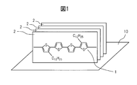
- FIG. 1 is a diagram for conceptually explaining an organic semiconductor film used in the present invention.
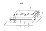
- FIG. 2 is a diagram for conceptually explaining a conventional organic semiconductor film.
- FIG. 3 is a diagram for conceptually explaining the organic semiconductor film used in the present invention.
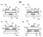
- FIG. 4 is a diagram illustrating a thin film transistor of the present invention.
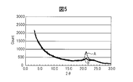
- FIG. 5 is a diagram showing the results of in-plane X-ray diffraction (XRD) analysis of the organic semiconductor film obtained in Example 1.
- FIG. 6 is a diagram showing the results of in-plane X-ray diffraction (XRD) analysis of the organic semiconductor film obtained in Example 3.
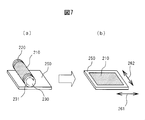
- FIG. 7 is a diagram for conceptually explaining the method of the present invention for producing an organic semiconductor film.
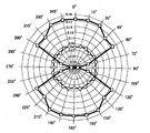
- FIG. 8 is a diagram showing the direction dependency of mobility for the organic semiconductor films of Examples 1A and 8A.
- the thin film transistor of the present invention includes a source electrode, a drain electrode, a gate electrode, a gate insulating film, and an organic semiconductor film, the source electrode and the drain electrode are insulated from the gate electrode by the gate insulating film, and the gate electrode The current flowing through the organic semiconductor film from the source electrode to the drain electrode is controlled by the voltage applied to.
- the molecular axis that maximizes the mobility of the organic semiconductor material is the channel length direction of the organic semiconductor element, that is, the electric field between the source electrode and the drain electrode in the plane of the organic semiconductor film. Oriented in the direction. Specifically, for example, in this organic semiconductor film, the direction of the molecular axis of the main chain of the organic semiconductor material is within ⁇ 60 ° of the direction of the electric field between the source electrode and the drain electrode in the plane of the organic semiconductor film. , Within ⁇ 45 °, within ⁇ 30 °, within ⁇ 20 °, or within ⁇ 10 °.
- the organic semiconductor film may not be in contact with the alignment film that aligns the organic semiconductor material in the plane direction.
- such an alignment film may not be provided directly below.
- the surface (2) formed by the aromatic ring constituting the organic semiconductor material (1) is substantially perpendicular to the substrate (10).
- the organic semiconductor material (1) is oriented in the plane of the organic semiconductor film.
- the fact that the surface (2) is a conformation standing substantially perpendicular to the substrate (10) and being uniaxially oriented is, for example, in in-plane X-ray diffraction (XRD) analysis. This can be confirmed by observing only the peaks due to the spacing between the surfaces.
- XRD in-plane X-ray diffraction
- Patent Document 2 when an organic semiconductor material in a solution state or a molten state is formed while applying strong shearing, an organic film is used without using an alignment film.
- the orientation of the semiconductor material can be achieved, as shown in FIG. 2, the surface (2 ′) formed by the aromatic ring (1) constituting the organic semiconductor material is substantially parallel to the substrate (10). It is known that the film is oriented so as to have a stacked structure (Non-patent Document 5).
- this surface (2 ′) is a layered structure substantially parallel to the substrate (10) is, for example, in the out-of-plane X-ray diffraction (XRD) analysis, this surface ( 2 ′) diffraction peaks are confirmed, and in the in-plane X-ray diffraction (XRD) analysis, a plurality of lamellar peaks due to the crystallization direction along the alkyl side chain (C 12 H 25 ) This can be confirmed by observation.
- XRD out-of-plane X-ray diffraction
- the surface (2) formed by the aromatic ring constituting the organic semiconductor material (1) has a conformation (edge-on-conformation (FIG. 1)) in which the surface (2) stands substantially perpendicular to the substrate (10).
- the molecular axis direction of the main chain of the organic semiconductor material is uniaxially oriented in the direction of the electric field between the source electrode and the drain electrode in the plane of the organic semiconductor film.
- a large charge mobility can be achieved in the direction of this electric field.
- an unoriented organic semiconductor film has a large variation in the orientation direction of the organic semiconductor material, which causes a problem that characteristic variations of thin film transistors using such an organic semiconductor film are likely to occur.
- the organic semiconductor film used in the present invention is uniaxially oriented, such variation in characteristics is reduced.
- the surface formed by the aromatic ring constituting the organic semiconductor material has a conformation standing substantially perpendicular to the substrate, and the molecular axis of the main chain of the organic semiconductor material Is oriented in the direction of the electric field between the source electrode and the drain electrode in the plane of the organic semiconductor film, a thin film transistor that functions at a relatively high speed can be obtained.
- organic semiconductor film used in the present invention when the organic semiconductor film used in the present invention is not in contact with an alignment film that aligns the organic semiconductor material in the plane direction, such an alignment film may have an undesirable effect on the organic semiconductor film, for example, alignment.
- an alignment film When a defect occurs in the film and / or when the alignment film deteriorates, it is possible to avoid a decrease in the characteristics of the organic semiconductor film.
- polyimide which is mainly used for the alignment film for aligning the organic semiconductor material in the plane direction, has a relatively high surface energy, so that the organic semiconductor film in contact therewith is disadvantageous in terms of electrical characteristics, and the organic semiconductor aromatic ring is a substrate.
- the organic semiconductor film of the present invention that is not in contact with the alignment film, such a problem can be avoided.
- the organic semiconductor film used in the thin film transistor of the present invention can be manufactured by the method of the present invention for manufacturing an organic semiconductor film.
- the maximum value of the ratio of the charge mobility in any two directions in the plane ⁇ (charge mobility in the direction in which the charge mobility is maximum) / (charge mobility in the direction in which the charge mobility is minimum) ⁇ May be greater than 1.5. That is, for example, as shown in FIG. 3, in the organic semiconductor film (20) of the present invention disposed on the substrate (10), the charge mobility in the direction (arrow 22) in which the charge mobility is maximum. However, it may be larger than 1.5 times the charge mobility in the direction (arrow 24) in which the charge mobility is minimum.
- the ratio value or maximum value of the charge mobility is, for example, 2 or more, 10 or more, 20 or more, and may be 50 or less, 30 or less, 20 or less, or 15 or less.
- the charge mobility in the direction in which the mobility is maximum is, for example, 0.01 cm 2 / (V ⁇ s) or more, 0.05 cm 2 / (V ⁇ s) or more, or 0 It may be 10 cm 2 / (V ⁇ s) or more.
- the charge mobility ⁇ cm 2 / (V ⁇ s) ⁇ is the charge mobility on the surface of the organic semiconductor film, and represents the ease of movement of charges that are holes or electrons. .
- the organic semiconductor film used in the present invention can have an arbitrary thickness, for example, a thickness of 1 nm to 1 ⁇ m, or 10 nm to 500 nm.
- Organic semiconductor material constituting the organic semiconductor film used in the present invention is an arbitrary organic semiconductor having an aromatic ring, and particularly an organic semiconductor material that can be in a liquid crystal state.
- organic semiconductor materials include low molecular organic semiconductor molecules such as pentacene, thiophene, perylene, and fullerene materials, polyalkylthiophene, polyphenylene vinylene, polyfluorene-thiophene copolymers, and the like. Mention may be made of molecular organic semiconductor molecules.
- the temperature at which the organic semiconductor material can be in a liquid crystal state is exemplified below:
- the organic semiconductor film used in the present invention can be produced by any method. It may be preferable in terms of productivity to manufacture the organic semiconductor film by a solution method, that is, a printing method such as a casting method, a spin coating method, or a contact printing method, or a dipping method.
- a solution method that is, a printing method such as a casting method, a spin coating method, or a contact printing method, or a dipping method.
- the organic semiconductor film of the present invention is a film obtained by a solution method, it is distinguished from those produced by other methods by the presence of a trace amount of solvent remaining in the organic semiconductor film, the shape and physical properties of the film, etc. be able to.
- the organic semiconductor film of the present invention can be produced, for example, by the method of the present invention for producing an organic semiconductor film.
- layers other than the organic semiconductor film of the thin film transistor of the present invention may be made of an inorganic material or an organic material.
- the electric circuit of the present invention has 100 or more, 1,000 or more, 10,000 or more, or 100,000 or more thin film transistors, and at least 80%, at least 90%, at least of these thin film transistors. 95% is the thin film transistor of the present invention.
- a first inventive method for producing an organic semiconductor film comprises providing an organic semiconductor solution in which an organic semiconductor material is dissolved and / or dispersed, applying the organic semiconductor solution onto a stamp and drying, Obtaining an organic semiconductor film on the stamp, and transferring the organic semiconductor layer at a temperature at which the organic semiconductor material becomes liquid crystal.
- the organic semiconductor layer is transferred at a temperature at which the organic semiconductor material becomes liquid crystal, thereby enabling transfer by the stamp and the base material.
- the surface formed by the aromatic ring constituting the organic semiconductor material can be aligned in a conformation that is substantially perpendicular to the substrate Become.
- the aromatic ring of the organic semiconductor material is self-organized in a conformation that is substantially perpendicular to the stamp at the air side interface. This is presumably because air is theoretically superhydrophobic and therefore has little influence on the organic semiconductor, whereby the organic semiconductor material itself takes the most stable conformation at least on the air side of the organic semiconductor film.
- the aligned organic semiconductor film (210) in the liquid crystal state is transferred from the stamp (220) to the base material (250) using a roller (230), for example, 220) and the substrate (250) are subjected to stress, particularly shear stress, on the organic semiconductor film (210).
- the aromatic ring of the organic semiconductor material of the organic semiconductor film (210) maintains a conformation that is preliminarily standing substantially perpendicular to the stamp.
- it is considered to be oriented with respect to the rotation direction (261) of the roller indicated by the arrow (231) or the vertical direction (262) thereof.
- the transfer temperature within the liquid crystal phase temperature range of the organic semiconductor film, the organic semiconductor film becomes a liquid crystal phase, and molecular orientation is facilitated even with a slight shear stress.
- the organic semiconductor layer can be transferred from the stamp to a substrate or film.
- a substrate or film may be any substrate or film that is intended to have an organic semiconductor film disposed thereon.
- examples of such a substrate include an inorganic material such as a silicon wafer and glass, and an organic material such as a polymer film.
- this substrate or film may have a contact angle with water of 50 degrees or more, 60 degrees or more, 70 degrees or more, 80 degrees or more, 90 degrees or more, or 100 degrees or more. That is, this substrate or film may be a substrate or film having a low surface energy.
- the organic semiconductor film is transferred to the substrate or film having a low surface energy by the method of the present invention, the surface formed by the aromatic ring constituting the organic semiconductor material is substantially perpendicular to the substrate. It becomes easy to take formation.
- the stamp to which the organic semiconductor solution is applied in the method of the present invention has a surface having a relatively large contact angle with water, that is, for example, a contact angle with water of 40 ° or more, 50 ° or more, 60 ° or more, 70 ° or more, 80 You may have the surface which is (degree) or more, 90 degree or more, 100 degree or more, or 105 degree or more.
- a relatively large contact angle of the surface of the substrate with water means that the surface is relatively lyophobic, that is, the surface energy of the surface is relatively small.
- the adhesion between the obtained organic semiconductor film and the transfer portion is relatively weak, and therefore, a relatively lyophobic substrate.
- the organic semiconductor film can be transferred onto the surface of the material, that is, the surface of the substrate having a contact angle with water of 50 ° or more, for example.
- the transfer part of a general contact print stamp is generally a lyophilic solution in order to improve the wettability with respect to the organic semiconductor solution thereon, thereby enabling the stable formation of a film of the organic semiconductor solution.
- a transfer portion of a conventional contact print stamp the adhesion between the obtained organic semiconductor film and the transfer portion is relatively strong, and therefore relatively lyophobic. It has been difficult to transfer the organic semiconductor film onto the surface of the substrate, that is, the surface of the substrate having a contact angle with water of 50 ° or more, for example.
- a stamp having a surface with a relatively large contact angle with water can be obtained, for example, by treating the surface of the stamp with a lyophobic material.
- lyophobic materials include silane, silazane, fluorine compounds, polyimide, polyester, polyethylene, polyphenylene sulfide, polyparaxylene, polyethylene terephthalate, polyethylene naphthalate, polydimethylsiloxane, and combinations thereof. it can.
- any method such as a casting method, a spin coating method, or a dipping method can be used.
- the organic semiconductor solution applied on the stamp is dried to obtain the organic semiconductor film on the stamp.
- this drying can be performed, for example, by exposing the organic semiconductor solution on the stamp to an atmosphere of more than 40 ° C., 50 ° C., 70 ° C. or 100 ° C. This drying can also be performed by removing the solvent from the organic semiconductor solution under reduced pressure.
- the organic semiconductor film on the stamp can be directly transferred onto a substrate such as a silicon wafer or a polymer film. Also, the organic semiconductor film on the stamp can be transferred to another stamp and transferred from the other stamp to the substrate.
- the transfer of the organic semiconductor film from the first stamp to the base material or another stamp can be achieved by bringing the stamp holding the organic semiconductor film into contact with the base material or another stamp.
- the transfer conditions such as the contact time, the stamp, and the temperature of the base material can be arbitrarily determined so that the organic semiconductor material becomes liquid crystal and can be transferred.
- this transfer can be performed such that the temperature of the base material or other stamp is higher than the temperature of the stamp.
- This transfer also treats the surface of the stamp to reduce adhesion to the organic semiconductor film and / or treats the surface of the substrate or other stamp to increase adhesion to the organic semiconductor film. Can be achieved. Still further, this transfer can be achieved by a combination of the above.
- the other stamp used in the method of the present invention is an arbitrary stamp that can transfer an organic semiconductor film formed on the stamp, and from which the organic semiconductor film can be transferred to a substrate, That is, it may be a contact print stamp.
- Such other stamps can be made of, for example, polysiloxane.
- the transfer of the organic semiconductor film from another stamp to the base material can be performed as described for the transfer of the organic semiconductor film from the stamp to the base material or another stamp.
- the method of the second present invention for producing an organic semiconductor film includes a step of providing an organic semiconductor film made of an organic semiconductor material having an aromatic ring on a substrate or film, and a temperature at which the organic semiconductor material is liquid crystallized. Applying an external stress to the layer to orient the organic semiconductor material in the plane of the organic semiconductor film.
- the provision of the organic semiconductor film on the substrate or film can be performed by any method, for example, a casting method, a spin coating method, a printing method such as a contact printing method, a solution method such as a dipping method, and the like. It can be provided using a vapor deposition method in which an organic semiconductor material is vapor-deposited on a substrate.
- an external stress is applied to the organic semiconductor layer at a temperature at which the organic semiconductor material becomes liquid crystal, particularly a shear stress, for example, the stamp is pressed against the base material
- a shear stress for example, the stamp is pressed against the base material
- the organic semiconductor film of the present invention can be produced.
- BGTC type bottom gate / top contact type
- Water contact angle The water contact angle was measured with pure water at 25 ° C. using a water contact angle meter CA-X manufactured by Kyowa Interface Science.
- Charge mobility The charge mobility of the organic semiconductor film was evaluated using a 4200-SCS type semiconductor evaluation apparatus manufactured by Keithley. The standard deviation of charge mobility was calculated by evaluating the characteristics of 10 or more elements.
- Example 1 (Production of stamps for contact printing) A silicone rubber (SIM-260 manufactured by Shin-Etsu Chemical Co., Ltd.) was cured into a flat plate shape, and oligomers were removed using hexane as a stamp material.
- the stamp material is cut into 20 mm square, a mask corresponding to the transfer portion is placed on the stamp material, the transfer portion is masked, and the stamp material in which the transfer portion is thus masked is subjected to UV (ultraviolet) -ozone treatment. Performed for 30 minutes. That is, the transfer portion was not subjected to UV-ozone treatment, and the peripheral portion was subjected to UV-ozone treatment. This UV-ozone treatment provided a lyophilic surface at the periphery.
- the water contact angle of the transfer part not subjected to UV-ozone treatment was 110 °, and the water contact angle of the peripheral part subjected to UV-ozone treatment for 30 minutes was 44 °. Further, twelve transfer portions exist on the stamp, and the size of each transfer portion was 100 ⁇ m ⁇ 2 mm.
- PQT Poly [bis (3-dodecyl-2-thienyl) -2,2′-dithiophene-5,5′-diyl]
- a mass part was dissolved by heating in 99.5 parts by mass of toluene to obtain a PQT solution as an organic semiconductor solution.
- This PQT solution was spin coated (1800 rpm, 20 seconds) onto the patterned stamp material. Thereafter, the PQT solution was aged and dried for about 10 minutes as it was, thereby forming an organic semiconductor film on the stamp.
- n-type silicon wafer with a 300 nm thermal oxide film (plane orientation ⁇ 100>, specific resistance 0.05 ⁇ ) was treated with hot concentrated sulfuric acid for 30 minutes, and then several times using pure water, acetone, toluene, and hexane. Ultrasonic cleaning was performed twice. Further, after cleaning for 30 minutes with a UV ozone cleaning device, surface treatment was performed with octadecyltrichlorosilane (OTS). In addition, the process of the base material by OTS was performed as follows.
- a 20 mM toluene solution of OTS was prepared.
- the above silicon substrate was immersed in the obtained OTS solution and held for 7 days. After soaking, the substrate was washed with toluene and ethanol and ultrasonically washed in ethanol for 30 minutes. All the steps so far were performed in a glove box in which the humidity was controlled to 3% or less. Thereafter, the substrate was washed with pure water and heat-treated at 100 ° C. for 5 minutes to obtain an OTS-treated substrate.
- the stamp which has an organic-semiconductor film was fixed to the roller, and the roller with a stamp was obtained.
- the silicon substrate was heated and held at 135 ° C., the above-mentioned stamped roller was brought into contact therewith, and rotated to transfer the entire organic semiconductor film to the substrate.
- Example 1A In the same manner as in Example 1, a PQT film was formed, and a source electrode and a drain electrode were formed to obtain a thin film transistor.
- the moving direction of the roller (the direction in which the mobility is maximum, that is, the direction of the molecular axis of the main chain of the organic semiconductor material) and the direction of the electric field between the source electrode and the drain electrode The angle between them was set to 0 °, 15 °, 30 °, 45 °, 60 °, 75 °, and 90 °.
- Example 2 The same procedure as in Example 2 was performed except that the transfer temperature was 140 ° C. The evaluation results are shown in Table 2.
- Example 3 The same procedure as in Example 1 was performed except that the transfer temperature was 130 ° C.
- the evaluation results are shown in Table 2.
- FIG. 6 shows the result of in-plane X-ray diffraction measurement of the transfer film in the direction parallel to and perpendicular to the transfer direction.
- a peak in the (010) direction is observed, but the X-ray diffraction intensity is clearly different between the parallel direction A and the vertical direction B, indicating that the PQT film is uniaxially oriented.
- FIG. 6 only the (010) peak is observed, and it is clear that the thiophene ring has a conformation that stands perpendicular to the substrate.
- Example 5 (Comparison) In the same manner as in Example 1, a PQT thin film was formed on the stamp. Same as Example 1 except that the solvent was dried by allowing it to stand for 10 minutes, and then the PQT thin film was heat-treated at 130 ° C. for 10 minutes under reduced pressure and transferred to the substrate at a transfer temperature of 80 ° C. Implemented. The evaluation results are shown in Table 2.
- Example 6 (Comparison) The same procedure as in Example 1 was performed except that the transfer temperature was 80 ° C. The evaluation results are shown in Table 2.
- Example 7 (Comparison) The device fabricated in Example 6 was heat-treated at 135 ° C. for 5 minutes under vacuum. The evaluation results are shown in Table 2.
- Example 8 (Comparison) The same procedure as in Example 7 was performed, except that a PQT film was directly formed on the substrate by spin coating using a 0.5% toluene solution of PQT. The evaluation results are shown in Table 2.
- Example 8A (comparison) >> In the same manner as in Example 8, a PQT film was formed, and a source electrode and a drain electrode were formed to obtain a thin film transistor.
- the moving direction of the roller (the direction in which the mobility is maximum, that is, the direction of the molecular axis of the main chain of the organic semiconductor material) and the direction of the electric field between the source electrode and the drain electrode The angle between them was set to 0 °, 15 °, 30 °, 45 °, 60 °, 75 °, and 90 °.
- Example 9 (Comparison) A device was fabricated in the same manner as in Example 1 except that polyhexylthiophene (P3HT: Poly (3-HexylThiophene)) (Plexcores Inc. Plexcore OS1100) was used as the organic semiconductor. Thereafter, heat treatment was performed at 100 ° C. for 30 minutes under vacuum, and the characteristics were measured. The evaluation results are shown in Table 2.
- P3HT Poly (3-HexylThiophene)
- Plexcore OS1100 Plexcore OS1100
- Example 10 Poly [(9,9-dioctylfluorenyl-2,7-diyl) -co-bithiophene] (“F8T2”) (ADS2008P molecular weight 43000, dispersion 2.8, manufactured by American Dye Source) was used as an organic semiconductor, and was transferred. The same operation as in Example 1 was conducted except that the temperature was 280 ° C. The evaluation results are shown in Table 2.
- Example 12 (Comparison) The same procedure as in Example 10 was performed except that a F8T2 0.5% toluene solution was used to directly form an F8T2 film on the substrate by spin coating. The evaluation results are shown in Table 2.
- Example 12A (Comparison)
- F8T2 poly [(9,9-dioctylfluorenyl-2,7-diyl) -co-bithiophene]
- a thin film transistor was prepared in accordance with Non-Patent Document 7, except that the transfer temperature was 280 ° C., that is, an organic semiconductor layer was formed while applying strong shearing. The evaluation results are shown in Table 2.
- Example 13 Except that poly (2,5-bis (3-tetradecylthiophen-2-yl) thieno [3,2, b] thiophene) (“pBTTT-C14”) was used as the organic semiconductor and the transfer temperature was 150 ° C. The same procedure as in Example 1 was performed. The evaluation results are shown in Table 2.
Landscapes
- Chemical & Material Sciences (AREA)
- Engineering & Computer Science (AREA)
- Materials Engineering (AREA)
- Thin Film Transistor (AREA)
Abstract
本発明は、新規な薄膜トランジスタ及びその製造方法、並びにこのような薄膜トランジスタを有する電気回路を提供するものである。 本発明の薄膜トランジスタは、ソース電極、ドレイン電極、ゲート電極、ゲート絶縁膜、及び有機半導体膜を有し、ゲート絶縁膜によって、ソース電極及びドレイン電極が、ゲート電極から絶縁されており、かつゲート電極に印加される電圧によって、ソース電極からドレイン電極へと半導体膜を通って流れる電流が制御される。ここで、前記有機半導体膜が、芳香環を有する有機半導体材料(1)からなり、有機半導体材料を構成する芳香環によって形成される面(2)が、基板(10)に対して略垂直に立ったコンフォメーションであり、かつ有機半導体材料(1)の移動度が最大となる分子軸が、 有機半導体膜の面内において、ソース電極とドレイン電極との間の電界の方向に配向している。
Description
本発明は、新規な薄膜トランジスタ及びその製造方法、並びにこのような薄膜トランジスタを有する電気回路に関する。
近年、半導体膜は、薄膜トランジスタ(TFT)に代表される半導体素子、太陽電池等のさまざまな用途に用いられるようになっている。
現在主に用いられている無機半導体膜、特にシリコンを半導体材料として用いる無機半導体膜は、製造時に化学気相成長(CVD)やスパッタリング等の真空プロセスを用いることから、製造コストが高い。また、無機半導体膜では、プロセス温度の点から、高分子フィルム等の上に形成することが難しい。またさらに、無機半導体膜は、将来的に実用化が期待される軽量でフレキシブルな素子やRF-ID(Radio Frequency IDentification)等の低コストの要求に答えることが難しい。
上記のような課題を解決するために、有機半導体材料から作られた有機半導体膜を用いることが提案されている。有機半導体膜の製造で用いる真空蒸着装置や塗布装置は、無機半導体膜の製造で用いられるCVD装置やスパッタリング装置と比較して安価である。また、有機半導体膜の製造では、プロセス温度が低いため、有機半導体膜を高分子フィルムや紙等の上に半導体膜を形成することも可能である。
ここで、有機半導体膜の形成方法としては、有機半導体材料を含有する溶液を、基材、スタンプ等に塗布し、そして溶媒を除去する溶液法(例えばキャスト法、スピンコート法、コンタクトプリント法のようなプリント法、ディップ法等)、及び有機半導体材料を基材に蒸着させる蒸着法が知られている。これらの方法のうちの溶液法は一般に、製造コスト、製造速度等に関して好ましいことが知られており、したがって様々な研究がなされている。しかしながら、溶液法によって質の高い有機半導体膜を安定的に得ることは、必ずしも充分に達成されていなかった。
有機半導体の電荷移動度は、その結晶性、結晶形態に強く依存することが知られており、単結晶の有機半導体における電荷移動度は、その結晶方位に依存することが知られている。したがって、有機半導体の特性を最大限に引き出すために、結晶性の有機半導体膜を面内配向させ、移動度が最大となる分子軸を有機半導体素子のチャネル長方向に配向させることが提案されている。
これに関して、特許文献1、並びに非特許文献1及び2では、ラビング(擦り)処理されたポリマー層等である配向膜を基材上に形成し、この配向膜上に有機半導体膜を成膜し、そして有機半導体膜を液晶転移温度まで昇温させて、配向膜の作用によって有機半導体膜を配向させ、それによって面内に一軸異方性を有する有機半導体膜を形成することを提案している。すなわち、これらの文献では、有機半導体材料を面方向に配向させるための配向膜上に有機半導体膜を形成することを提案している。
また、特許文献2、並びに非特許文献3~7では、溶液状態又は溶融状態の有機半導体材料を、強い剪断を与えながら成膜することにより、一軸異方性を有する有機半導体層を形成することを提案している。
なお、特許文献3では、有機半導体材料を基材に対して垂直方向に配向させる配向膜を基材上に形成し、有機半導体膜を、スタンプ等の離型性基板からこの配向膜上に、液晶相温度で転写して、配向膜の作用によって有機半導体膜を基材に対して垂直方向に配向させることを提案している。すなわち、この文献では、有機半導体材料を基材に対して垂直方向に配向させることによって、有機半導体膜の面内方向における移動度を向上させることを提案している。
H.Sirringhaus etc., Mobility enhancement in conjugated polymer field-effect transistor through chain alignment in a liquid-crystaline phase"Appl. Phys. Lett., VOL. 77, NO. 3, 17, 2000, 406-408
L.Kindera etc., "Structural ordering and enhanced charier mobility in organic polymer thin film transistors" Synthetic Metals, 146, 2004, 181-185
A.Hector etc., "High-performance organic thin-film transistors through solution-sheared deposition of small-molecule organic semiconductors" Adv. Matter., 20, 2008, 2588-2594
M.Karakawa etc., "High-performance poly(3-hexylthiophene) field-effect transistors fabricated by a slide-coating method" Applied Physics Express 1 (2008) 061802
S.Nagamatsu etc., "Backbone Arrangement in "Friction-Transferred" Regioregular Poly(3-alkylthiphene)s" Macromolecules, 36 (2003) 5252
J.-F.Chang etc., "Enhanced Mobility of Poly(3-hexylthiophene) Transistors by Spin-Coating from High-Boiling-Point Solvents" Chem. Mater., 16 (2004) 4772
Y.Koshiba etc., "Fabrication of One-Dimensionally Oriented Fluoren-Thiophene Copolymer Thin Films and Anisotropic Transistor Characterization" Jpn. J. Appll. Phys., 49 (2010)01AE13
本発明の目的は、新規な薄膜トランジスタ及びその製造方法、並びにこのような薄膜トランジスタを有する電気回路を提供することである。
本件発明者等は、有機半導体材料を構成する芳香環によって形成される面が、基板に対して略垂直に立ったコンフォメーションであり、かつ有機半導体材料が、有機半導体膜の面内で配向している有機半導体膜を、特定の方法で成膜できることを見出して、下記の薄膜トランジスタ及びその製造方法、並びに電気回路に想到した。
〈1〉ソース電極、ドレイン電極、ゲート電極、ゲート絶縁膜、及び有機半導体膜を有し、ゲート絶縁膜によって、ソース電極及びドレイン電極が、ゲート電極から絶縁されており、かつゲート電極に印加される電圧によって、ソース電極からドレイン電極へと半導体膜を通って流れる電流が制御される、薄膜トランジスタであって、
上記有機半導体膜が、芳香環を有する有機半導体材料からなり、
上記有機半導体材料を構成する芳香環によって形成される面が、基板に対して略垂直に立ったコンフォメーションであり、かつ
上記有機半導体材料の移動度が最大となる分子軸が、有機半導体膜の面内において、ソース電極とドレイン電極との間の電界の方向に配向している、
薄膜トランジスタ。
〈2〉上記有機半導体材料の主鎖の分子軸の方向が、有機半導体膜の面内において、ソース電極とドレイン電極との間の電界の方向の±60°以内である、上記〈1〉項に記載の薄膜トランジスタ。
〈3〉上記有機半導体材料を面方向に配向させる配向膜に接していない、上記〈1〉又は〈2〉項に記載の薄膜トランジスタ。
〈4〉面内で直行する2方向の電荷移動度の比{(電荷移動度が最大である方向の電荷移動度)/(それと直行する方向の電荷移動度)}の値が1.5より大きい、上記〈1〉~〈3〉項のいずれか一項に記載の薄膜トランジスタ。
〈5〉上記有機半導体膜がコンタクトプリント法よって得られたものである、上記〈1〉~〈4〉項のいずれか一項に記載の薄膜トランジスタ。
〈6〉上記有機半導体材料が、液晶状態になり得る有機半導体材料である、上記〈1〉~〈5〉項のいずれか一項に記載の薄膜トランジスタ。
〈7〉上記電荷移動度の比の値が5以上である、上記〈1〉~〈6〉項のいずれか一項に記載の薄膜トランジスタ。
〈8〉上記有機半導体膜の電荷移動度が最大となる方向の電荷移動度が、0.01cm2/(V・s)以上である、上記〈1〉~〈7〉項のいずれか一項に記載の薄膜トランジスタ。
〈9〉上記有機半導体膜が、水に対する接触角が50度以上である基板又は膜に接している、上記〈1〉~〈8〉項のいずれか一項に記載の薄膜トランジスタ。
〈10〉薄膜トランジスタを100個以上有する電気回路であって、
上記薄膜トランジスタのうちの少なくとも80%が、上記〈1〉~〈9〉項のいずれか一項に記載の薄膜トランジスタである、
電気回路。
〈11〉有機半導体材料が溶解及び/又は分散している有機半導体溶液を提供するステップ、
上記有機半導体溶液を、スタンプ上に適用し、乾燥させて、上記スタンプ上に有機半導体膜を得るステップ、
上記有機半導体層を、上記有機半導体材料が液晶化する温度で転写するステップ
を含む方法によって上記有機半導体膜を製造する、上記〈1〉~〈9〉項のいずれか一項に記載の薄膜トランジスタの製造方法。
〈12〉上記転写するステップを、印刷面に上記スタンプを有するロールを用いて行なう、上記〈11〉項に記載の方法。
〈13〉芳香環を有する有機半導体材料からなる有機半導体膜を基板又は膜上に提供するステップ、
上記有機半導体材料が液晶化する温度で、上記有機半導体層に対して外部から応力を加えて、上記有機半導体材料を上記有機半導体膜の面内で配向させるステップ、
を含む方法によって上記有機半導体膜を製造する、上記〈1~9〉項のいずれか一項に記載の薄膜トランジスタの製造方法。
〈14〉上記有機半導体膜が、水に対する接触角が50度以上である基板又は膜に接している、上記〈11〉~〈13〉項のいずれか一項に記載の方法。
上記有機半導体膜が、芳香環を有する有機半導体材料からなり、
上記有機半導体材料を構成する芳香環によって形成される面が、基板に対して略垂直に立ったコンフォメーションであり、かつ
上記有機半導体材料の移動度が最大となる分子軸が、有機半導体膜の面内において、ソース電極とドレイン電極との間の電界の方向に配向している、
薄膜トランジスタ。
〈2〉上記有機半導体材料の主鎖の分子軸の方向が、有機半導体膜の面内において、ソース電極とドレイン電極との間の電界の方向の±60°以内である、上記〈1〉項に記載の薄膜トランジスタ。
〈3〉上記有機半導体材料を面方向に配向させる配向膜に接していない、上記〈1〉又は〈2〉項に記載の薄膜トランジスタ。
〈4〉面内で直行する2方向の電荷移動度の比{(電荷移動度が最大である方向の電荷移動度)/(それと直行する方向の電荷移動度)}の値が1.5より大きい、上記〈1〉~〈3〉項のいずれか一項に記載の薄膜トランジスタ。
〈5〉上記有機半導体膜がコンタクトプリント法よって得られたものである、上記〈1〉~〈4〉項のいずれか一項に記載の薄膜トランジスタ。
〈6〉上記有機半導体材料が、液晶状態になり得る有機半導体材料である、上記〈1〉~〈5〉項のいずれか一項に記載の薄膜トランジスタ。
〈7〉上記電荷移動度の比の値が5以上である、上記〈1〉~〈6〉項のいずれか一項に記載の薄膜トランジスタ。
〈8〉上記有機半導体膜の電荷移動度が最大となる方向の電荷移動度が、0.01cm2/(V・s)以上である、上記〈1〉~〈7〉項のいずれか一項に記載の薄膜トランジスタ。
〈9〉上記有機半導体膜が、水に対する接触角が50度以上である基板又は膜に接している、上記〈1〉~〈8〉項のいずれか一項に記載の薄膜トランジスタ。
〈10〉薄膜トランジスタを100個以上有する電気回路であって、
上記薄膜トランジスタのうちの少なくとも80%が、上記〈1〉~〈9〉項のいずれか一項に記載の薄膜トランジスタである、
電気回路。
〈11〉有機半導体材料が溶解及び/又は分散している有機半導体溶液を提供するステップ、
上記有機半導体溶液を、スタンプ上に適用し、乾燥させて、上記スタンプ上に有機半導体膜を得るステップ、
上記有機半導体層を、上記有機半導体材料が液晶化する温度で転写するステップ
を含む方法によって上記有機半導体膜を製造する、上記〈1〉~〈9〉項のいずれか一項に記載の薄膜トランジスタの製造方法。
〈12〉上記転写するステップを、印刷面に上記スタンプを有するロールを用いて行なう、上記〈11〉項に記載の方法。
〈13〉芳香環を有する有機半導体材料からなる有機半導体膜を基板又は膜上に提供するステップ、
上記有機半導体材料が液晶化する温度で、上記有機半導体層に対して外部から応力を加えて、上記有機半導体材料を上記有機半導体膜の面内で配向させるステップ、
を含む方法によって上記有機半導体膜を製造する、上記〈1~9〉項のいずれか一項に記載の薄膜トランジスタの製造方法。
〈14〉上記有機半導体膜が、水に対する接触角が50度以上である基板又は膜に接している、上記〈11〉~〈13〉項のいずれか一項に記載の方法。
本発明の薄膜トランジスタは、比較的高速で機能することができる。また、有機半導体膜を生成する本発明の方法によれば、本発明の薄膜トランジスタで用いられる有機半導体膜を生成することができる。
《薄膜トランジスタ》
本発明の薄膜トランジスタは、ソース電極、ドレイン電極、ゲート電極、ゲート絶縁膜、及び有機半導体膜を有し、ゲート絶縁膜によって、ソース電極及びドレイン電極が、ゲート電極から絶縁されており、かつゲート電極に印加される電圧によって、ソース電極からドレイン電極へと有機半導体膜を通って流れる電流が制御される。
本発明の薄膜トランジスタは、ソース電極、ドレイン電極、ゲート電極、ゲート絶縁膜、及び有機半導体膜を有し、ゲート絶縁膜によって、ソース電極及びドレイン電極が、ゲート電極から絶縁されており、かつゲート電極に印加される電圧によって、ソース電極からドレイン電極へと有機半導体膜を通って流れる電流が制御される。
本発明の薄膜トランジスタでは、有機半導体膜は、芳香環を有する有機半導体材料からなる。ここで、この有機半導体膜では、有機半導体材料を構成する芳香環によって形成される面が、基板に対して略垂直に立ったコンフォメーションである。
また、この有機半導体膜では、有機半導体材料の移動度が最大となる分子軸が、有機半導体膜の面内において、有機半導体素子のチャネル長方向、すなわちソース電極とドレイン電極との間の電界の方向に配向している。具体的には例えば、この有機半導体膜では、有機半導体材料の主鎖の分子軸の方向が、有機半導体膜の面内において、ソース電極とドレイン電極との間の電界の方向の±60°以内、±45°以内、±30°以内、±20°以内、又は±10°以内である。
この有機半導体膜は、有機半導体材料を面方向に配向させる配向膜に接していなくてもよく、例えば直下にこのような配向膜を有さなくてもよい。
(略垂直に立ったコンフォメーション)
本発明の薄膜トランジスタで用いられる有機半導体膜では、図1で示すように、有機半導体材料(1)を構成する芳香環によって形成される面(2)が、基板(10)に対して略垂直に立ったコンフォメーションをとった状態であり、かつ有機半導体材料(1)が、有機半導体膜の面内で配向している。
本発明の薄膜トランジスタで用いられる有機半導体膜では、図1で示すように、有機半導体材料(1)を構成する芳香環によって形成される面(2)が、基板(10)に対して略垂直に立ったコンフォメーションをとった状態であり、かつ有機半導体材料(1)が、有機半導体膜の面内で配向している。
ここで、この面(2)が、基板(10)に対して略垂直に立ったコンフォメーションであり、かつ一軸配向していることは例えば、in-planeのX線回折(XRD)解析において、この面の間隔に起因するピークのみが観察されることによって確認できる。
これに対して、特許文献2、並びに非特許文献3~5でのように、溶液状態又は溶融状態の有機半導体材料を、強い剪断を与えながら成膜する場合、配向膜を用いずに、有機半導体材料の配向を達成することができるものの、図2で示すように、有機半導体材料を構成する芳香環(1)によって形成される面(2’)が、基板(10)に対して略平行に積層されたコンフォメーションであるようにして配向していることが知られている(非特許文献5)。
このようにこの面(2’)が、基板(10)に対して略平行に積層されたコンフォメーションであることは例えば、out-of-planeのX線回折(XRD)解析において、この面(2‘)の回折ピークが確認されること、およびin-planeのX線回折(XRD)解析において、アルキル側鎖(C12H25)に沿った結晶化方向に起因する複数のラメラ晶ピークが観察されることによって確認できる。
これに関して、芳香環を有する有機半導体のコンフォメーションと半導体特性の関係については広く研究されている。具体的には、有機半導体材料(1)を構成する芳香環によって形成される面(2)が、基板(10)に対して略垂直に立ったコンフォメーション(エッジオンコンフォメーション(図1))を有する場合には、有機半導体材料を構成する芳香環(1)によって形成される面(2’)が、基板(10)に対して略平行に積層されたコンフォメーション(フェイスオンコンフォメーション(図2))よりも、電荷移動度をはじめとする半導体特性が優れていることが一般的に知られている(特許文献3、非特許文献1、6等)。
(主鎖の分子軸の方向)
本発明の薄膜トランジスタで用いられる有機半導体膜では、有機半導体材料の主鎖の分子軸の方向が、有機半導体膜の面内において、ソース電極とドレイン電極との間の電界の方向に一軸配向しており、それによってこの電界の方向において大きい電荷移動度を達成できる。なお、未配向の有機半導体膜では有機半導体材料の配向方向のばらつきが大きく、それによってそのような有機半導体膜を用いる薄膜トランジスタの特性ばらつきが生じやすいといった問題がある。これに対して、本発明で用いられる有機半導体膜は一軸配向していることによって、このような特性のばらつきが小さくなる。
本発明の薄膜トランジスタで用いられる有機半導体膜では、有機半導体材料の主鎖の分子軸の方向が、有機半導体膜の面内において、ソース電極とドレイン電極との間の電界の方向に一軸配向しており、それによってこの電界の方向において大きい電荷移動度を達成できる。なお、未配向の有機半導体膜では有機半導体材料の配向方向のばらつきが大きく、それによってそのような有機半導体膜を用いる薄膜トランジスタの特性ばらつきが生じやすいといった問題がある。これに対して、本発明で用いられる有機半導体膜は一軸配向していることによって、このような特性のばらつきが小さくなる。
したがって、本発明の薄膜トランジスタでのように、有機半導体材料を構成する芳香環によって形成される面が、基板に対して略垂直に立ったコンフォメーションであり、かつ有機半導体材料の主鎖の分子軸の方向が、有機半導体膜の面内において、ソース電極とドレイン電極との間の電界の方向に配向している場合、比較的高速で機能する薄膜トランジスタを得ることができる。
またさらに、本発明で用いられる有機半導体膜が、有機半導体材料を面方向に配向させる配向膜に接していない場合、このような配向膜が有機半導体膜に与えることがある好ましくない影響、例えば配向膜に欠陥が生じた場合及び/又は配向膜が劣化した場合のこれに伴う有機半導体膜の特性の低下を避けることができる。また更には、有機半導体材料を面方向に配向させる配向膜に主として用いられるポリイミドは比較的表面エネルギーが高いため、それに接する有機半導体膜は電気特性上不利となること、有機半導体の芳香環が基板に対して平行となるコンフォメーションを取り易くなることといったデメリットを有するが、このような配向膜に接していない本発明の有機半導体膜では、このような問題を避けることができる。
なお、本発明の薄膜トランジスタで用いられる有機半導体膜は、有機半導体膜を製造する本発明の方法によって製造することができる。
(電荷移動度)
本発明で用いられる有機半導体膜では、面内で直行する2方向の電荷移動度の比{(電荷移動度が最大である方向の電荷移動度)/(それと直行する方向の電荷移動度)}の値、又は面内の任意の2方向の電荷移動度の比の最大値{(電荷移動度が最大である方向の電荷移動度)/(電荷移動度が最小である方向の電荷移動度)}が、1.5より大きくてよい。すなわち例えば、図3で示されているように、基板(10)上に配置されている本発明の有機半導体膜(20)では、電荷移動度が最大である方向(矢印22)の電荷移動度が、電荷移動度が最小である方向(矢印24)の電荷移動度の1.5倍よりも大きくてよい。
本発明で用いられる有機半導体膜では、面内で直行する2方向の電荷移動度の比{(電荷移動度が最大である方向の電荷移動度)/(それと直行する方向の電荷移動度)}の値、又は面内の任意の2方向の電荷移動度の比の最大値{(電荷移動度が最大である方向の電荷移動度)/(電荷移動度が最小である方向の電荷移動度)}が、1.5より大きくてよい。すなわち例えば、図3で示されているように、基板(10)上に配置されている本発明の有機半導体膜(20)では、電荷移動度が最大である方向(矢印22)の電荷移動度が、電荷移動度が最小である方向(矢印24)の電荷移動度の1.5倍よりも大きくてよい。
ここで、この電荷移動度の比の値又は最大値は例えば、2以上、10以上、20以上であって、50以下、30以下、20以下、又は15以下であってよい。
本発明で用いられる有機半導体膜では、移動度が最大となる方向の電荷移動度が例えば、0.01cm2/(V・s)以上、0.05cm2/(V・s)以上、又は0.10cm2/(V・s)以上であってよい。ここで、本発明に関して電荷移動度{cm2/(V・s)}は、有機半導体膜の表面における電荷移動度であり、正孔又は電子である電荷の移動のしやすさを表している。
(厚さ)
本発明で用いられる有機半導体膜は任意の厚さを有することができ、例えば1nm~1μm、又は10nm~500nmの厚さを有することができる。
本発明で用いられる有機半導体膜は任意の厚さを有することができ、例えば1nm~1μm、又は10nm~500nmの厚さを有することができる。
(有機半導体材料)
本発明で用いられる有機半導体膜を構成する有機半導体材料は、芳香環を有する任意の有機半導体であり、特に液晶状態になり得る有機半導体材料である。このような有機半導体材料としては例えば、ペンタセン系、チオフェン系、ペリレン系、フラーレン系材料のような低分子系の有機半導体分子、ポリアルキルチオフェン、ポリフェニレンビニレン、ポリフルオレン-チオフェンコポリマー等のような高分子系の有機半導体分子を挙げることができる。
本発明で用いられる有機半導体膜を構成する有機半導体材料は、芳香環を有する任意の有機半導体であり、特に液晶状態になり得る有機半導体材料である。このような有機半導体材料としては例えば、ペンタセン系、チオフェン系、ペリレン系、フラーレン系材料のような低分子系の有機半導体分子、ポリアルキルチオフェン、ポリフェニレンビニレン、ポリフルオレン-チオフェンコポリマー等のような高分子系の有機半導体分子を挙げることができる。
なお、参考までに、有機半導体材料が液晶状態になりうる温度について、下記に例示する:

なお、表1における記号の意味は下記のとおりである:
PQT: ポリ[ビス(3-ドデシル-2-チエニル)-2,2‘-ジチオフェン-5,5’-ジイル]
F8T2: ポリ[(9,9-ジオクチルフルオレニル-2,7-ジイル)-co-ビチオフェン]
F8BT: ポリ[(9,9-ジオクチルフルオレニル-2,7-ジイル)-alt-ベンゾ[2,1,3]チアジアゾール-4,8-ジイル]
pBTTT(C10): ポリ(2,5-ビス(3-デシルチオフェン-2-イル)チエノ[3,2,b]チオフェン)
pBTTT(C12): ポリ(2,5-ビス(3-ドデシルチオフェン-2-イル)チエノ[3,2,b]チオフェン)
pBTTT(C14): ポリ(2,5-ビス(3-テトラデシルチオフェン-2-イル)チエノ[3,2,b]チオフェン)
PQT: ポリ[ビス(3-ドデシル-2-チエニル)-2,2‘-ジチオフェン-5,5’-ジイル]
F8T2: ポリ[(9,9-ジオクチルフルオレニル-2,7-ジイル)-co-ビチオフェン]
F8BT: ポリ[(9,9-ジオクチルフルオレニル-2,7-ジイル)-alt-ベンゾ[2,1,3]チアジアゾール-4,8-ジイル]
pBTTT(C10): ポリ(2,5-ビス(3-デシルチオフェン-2-イル)チエノ[3,2,b]チオフェン)
pBTTT(C12): ポリ(2,5-ビス(3-ドデシルチオフェン-2-イル)チエノ[3,2,b]チオフェン)
pBTTT(C14): ポリ(2,5-ビス(3-テトラデシルチオフェン-2-イル)チエノ[3,2,b]チオフェン)
ここで、相転移温度は、下記のようにして得ることができる。すなわち、示差走査熱量計を用いて、JIS K7121-1987「プラスチックの転移温度測定方法(Testing Methods for Transition Temperature of Plastics)」に準じた示差走査熱分析(DSC)で、予想される転移温度よりも約50℃低い温度において装置が安定するまで保持した後、加熱速度10℃/分で、予想される転移終了時よりも約30℃高い温度まで加熱して、示差走査熱分析曲線を得る。その後、得られた示差走査熱分析曲線について、液晶化及び溶融のピークの頂点を、それぞれ液晶相転移温度及び融解温度として特定する。示差走査熱量計としては例えば、ティー・エイ・インスツルメント(株)製の商品名:DSC Q10を用いることができる。
(製造方法)
本発明で用いられる有機半導体膜は任意の方法で製造することができる。この有機半導体膜は、溶液法、すなわち例えばキャスト法、スピンコート法、コンタクトプリント法のようなプリント法、ディップ法等で製造することが、生産性等に関して好ましいことがある。本発明の有機半導体膜が溶液法によって得られた膜である場合、有機半導体膜中に残留する微量の溶媒の存在、膜の形状及び物性等によって、他の方法によって作られたものと区別することができる。本発明の有機半導体膜は例えば、有機半導体膜を製造する本発明の方法によって製造することができる。
本発明で用いられる有機半導体膜は任意の方法で製造することができる。この有機半導体膜は、溶液法、すなわち例えばキャスト法、スピンコート法、コンタクトプリント法のようなプリント法、ディップ法等で製造することが、生産性等に関して好ましいことがある。本発明の有機半導体膜が溶液法によって得られた膜である場合、有機半導体膜中に残留する微量の溶媒の存在、膜の形状及び物性等によって、他の方法によって作られたものと区別することができる。本発明の有機半導体膜は例えば、有機半導体膜を製造する本発明の方法によって製造することができる。
なお、本発明の薄膜トランジスタの有機半導体膜以外の層、例えば電極層、誘電体層等の他の層は、無機材料で作られていても、有機材料で作られていてもよい。
例えば図4に示すように、本発明の薄膜トランジスタは、(a)ボトムゲート・トップコンタクト型(BGTC型)、(b)ボトムゲート・ボトムコンタクト型(BGBC型)、(c)トップゲート・トップコンタクト型(TGTC型)、及び(d)トップゲート・ボトムコンタクト型(TGBC型)のいずれであってもよい。これらの本発明の薄膜トランジスタ130、140、150及び160では、ソース電極134、144、154、164、ドレイン電極135、145、155、165、ゲート電極131、141、151、161、ゲート絶縁膜132、142、152、162、及び半導体膜133、143、153、163を有し、ゲート絶縁膜によって、ソース電極及びドレイン電極をゲート電極から絶縁されており、かつゲート電極に印加される電圧によって、ソース電極からドレイン電極へと半導体膜を通って流れる電流が制御される。
《電気回路》
本発明の電気回路は、薄膜トランジスタを100個以上、1,000個以上、10,000個以上、又は100,000個以上有し、かつこれらの薄膜トランジスタのうちの少なくとも80%、少なくとも90%、少なくとも95%が、本発明の薄膜トランジスタである。
本発明の電気回路は、薄膜トランジスタを100個以上、1,000個以上、10,000個以上、又は100,000個以上有し、かつこれらの薄膜トランジスタのうちの少なくとも80%、少なくとも90%、少なくとも95%が、本発明の薄膜トランジスタである。
このような本発明の電気回路によれば、高速で作用する本発明の薄膜トランジスタの特性を有益に利用することができる。
《有機半導体膜の製造方法-第1の方法》
有機半導体膜を製造する第1の本発明の方法は、有機半導体材料が溶解及び/又は分散している有機半導体溶液を提供するステップ、有機半導体溶液を、スタンプ上に適用し、乾燥させて、スタンプ上に有機半導体膜を得るステップ、有機半導体層を、有機半導体材料が液晶化する温度で転写するステップを含む。
有機半導体膜を製造する第1の本発明の方法は、有機半導体材料が溶解及び/又は分散している有機半導体溶液を提供するステップ、有機半導体溶液を、スタンプ上に適用し、乾燥させて、スタンプ上に有機半導体膜を得るステップ、有機半導体層を、有機半導体材料が液晶化する温度で転写するステップを含む。
有機半導体膜を製造するこの本発明の方法によれば、本発明の薄膜トランジスタで用いられる有機半導体膜を製造することができる。
具体的には、有機半導体膜を製造する本発明の方法によれば、有機半導体層を、有機半導体材料が液晶化する温度で転写することによって、スタンプによる転写を可能としつつ、スタンプと基材との間で液晶状態の有機半導体膜に応力をかけることによって、有機半導体材料を構成する芳香環によって形成される面を、基板に対して略垂直に立ったコンフォメーションで配向させることが可能になる。
理論によって限定されるものではないが、本発明の方法によって、この面を基板に対して略垂直に立ったコンフォメーションで配向させることができるのは、以下のような理由によると考えられる。
1. 溶液法を用いてスタンプ上に有機半導体膜を製膜する際、空気側界面では有機半導体材料の芳香環がスタンプに対して略垂直に立ったコンフォメーションで自己組織化する。これは空気が理論上超疎水性であるため、有機半導体に与える影響が少なく、それによって少なくとも有機半導体膜の空気側において、有機半導体材料自身が最も安定なコンフォメーションを取るためと考えられる。
2. 図6(a)で示すようにして、配向した液晶状態の有機半導体膜(210)を、例えばローラー(230)を用いてスタンプ(220)から基材(250)等に転写する場合、スタンプ(220)と基材(250)との間で有機半導体膜(210)に、応力、特に剪断応力がかる。これによれば、有機半導体膜(210)の有機半導体材料の芳香環が、スタンプに対して予め略垂直に立ったコンフォメーションを維持しつつ、図6(b)で示すように、特定の方向、例えば矢印(231)で示すローラーの回転方向(261)、又はその垂直方法(262)に対して配向すると考えられる。この際、転写温度を有機半導体膜の液晶相温度範囲とすることにより、有機半導体膜が液晶相となり、わずかな剪断応力に対しても分子配向をし易くなる。
(有機半導体材料及び溶媒)
本発明の方法で用いられる有機半導体材料については、本発明の有機半導体膜に関する記載を参照できる。
本発明の方法で用いられる有機半導体材料については、本発明の有機半導体膜に関する記載を参照できる。
本発明の方法で用いられる有機半導体溶液に含有されている溶媒は、有機半導体材料を溶解及び/又は分散させることができる任意の溶媒であってよい。このような溶媒としては、トルエン、キシレン、テトラリン、デカリン、クロロホルム、モノクロロベンゼン、ジクロロベンゼン、トリクロロベンゼン、及びそれらの組み合わせ等を挙げることができる。
(基材)
本発明の方法では、有機半導体層をスタンプから基材又は膜に転写することができる。このような基材又は膜は、有機半導体膜をその上に配置することを意図する任意の基材又は膜であってよい。したがって、例えばこのような基材としては、シリコンウェハ、ガラスのような無機材料、ポリマーフィルムのような有機材料を挙げることができる。
本発明の方法では、有機半導体層をスタンプから基材又は膜に転写することができる。このような基材又は膜は、有機半導体膜をその上に配置することを意図する任意の基材又は膜であってよい。したがって、例えばこのような基材としては、シリコンウェハ、ガラスのような無機材料、ポリマーフィルムのような有機材料を挙げることができる。
また、この基板又は膜は、水に対する接触角が50度以上、60度以上、70度以上、80度以上、90度以上、又は100度以上、であってよい。すなわち、この基板又は膜は、表面エネルギーが小さい基板又は膜であってよい。このように表面エネルギーが小さい基板又は膜に、本発明の方法によって有機半導体膜を転写する場合、有機半導体材料を構成する芳香環によって形成される面が、基板に対して略垂直に立ったコンフォメーションを取り易くなる。
(スタンプ)
また、本発明の方法で有機半導体溶液を適用されるスタンプは、有機半導体膜をその上で形成して、そしてそこから有機半導体膜を、基材等に転写することができる任意のスタンプ、すなわち有機半導体膜を形成するためのコンタクトプリント用スタンプであってよい。このようなスタンプは、印刷面にスタンプが配置されるようにしてロールに取り付け、そしてロールを回転させながらスタンプを基材等に押し付けて、転写を行わせることができる。
また、本発明の方法で有機半導体溶液を適用されるスタンプは、有機半導体膜をその上で形成して、そしてそこから有機半導体膜を、基材等に転写することができる任意のスタンプ、すなわち有機半導体膜を形成するためのコンタクトプリント用スタンプであってよい。このようなスタンプは、印刷面にスタンプが配置されるようにしてロールに取り付け、そしてロールを回転させながらスタンプを基材等に押し付けて、転写を行わせることができる。
本発明の方法において有機半導体溶液を適用されるスタンプは、水に対する接触角が比較的大きい表面、すなわち例えば水に対する接触角が、40°以上、50°以上、60°以上、70°以上、80°以上、90°以上、100°以上、又は105°以上である表面を有していてもよい。このように、基材の表面の水に対する接触角が比較的大きいことは、この表面が比較的疎液性であること、すなわちこの表面の表面エネルギーが比較的小さいことを意味している。
本発明の方法において用いることができるコンタクトプリント用スタンプは、転写部が周縁部よりも疎液性であるコンタクトプリント用スタンプである。ここで、疎液性であることは、表面エネルギーが小さいことを意味するので、このコンタクトプリント用スタンプは、転写部の表面エネルギーが小さく、かつ周縁部の表面エネルギーが大きい転写部-周縁部構造を有するコンタクトプリント用スタンプであるということができる。
このコンタクトプリント用スタンプの転写部上において、有機半導体溶液から有機半導体膜を形成する場合、疎液性の転写部の周囲に、親液性の周縁部が存在することによって、比較的濡れにくい転写部の表面に有機半導体溶液の膜を保持して、転写部の表面上で有機半導体溶液から有機半導体膜を形成することを促進できる。すなわち、このスタンプによれば、比較的濡れにくい転写部の表面上においても、有機半導体膜を形成できる。
また、このコンタクトプリント用スタンプの転写部上において、有機半導体溶液から有機半導体膜を形成する場合、得られた有機半導体膜と転写部との付着が比較的弱く、したがって比較的疎液性の基材の表面、すなわち例えば水に対する接触角が50°以上である基材の表面に、有機半導体膜を転写することができる。
なお、一般的なコンタクトプリント用スタンプの転写部は一般に、その上での有機半導体溶液に対する濡れ性を改良し、それによって有機半導体溶液の膜を安定的に形成を可能にするために、親液性にされている。したがって、従来のコンタクトプリント用スタンプの転写部上において、有機半導体溶液から有機半導体膜を形成する場合、得られた有機半導体膜と転写部との付着が比較的強く、したがって比較的疎液性の基材の表面、すなわち例えば水に対する接触角が50°以上である基材の表面に、有機半導体膜を転写することは難しかった。
本発明に関して、水に対する接触角は、25℃において、接触角を測定する表面上に50μLの水を滴下し、滴下した液滴の形状を側面から観察し、液滴と表面とのなす角度を計測することによって決定できる。
このように、本発明の方法において有機半導体溶液を適用されるスタンプが、低表面エネルギー表面を有する場合、有機半導体膜中の有機半導体材料は、スタンプに接している面においても、スタンプの表面の影響を受けにくく、したがって有機半導体材料自身の結晶性等によって再配列することが容易になる。
水に対する接触角が比較的大きい表面を有するスタンプは例えば、スタンプの表面を疎液性材料で処理することによって得ることができる。このような疎液性材料としては例えば、シラン、シラザン、フッ素化合物、ポリイミド、ポリエステル、ポリエチレン、ポリフェニレンスルフィド、ポリパラキシレン、ポリエチレンテレフタレート、ポリエチレンナフタレート、ポリジメチルシロキサン、及びそれらの組み合わせを挙げることができる。
(適用)
有機半導体膜を製造する本発明の方法において、有機半導体溶液をスタンプに適用するためには、キャスティング法、スピンコート法、ディッピング法等の任意の方法を用いることができる。
有機半導体膜を製造する本発明の方法において、有機半導体溶液をスタンプに適用するためには、キャスティング法、スピンコート法、ディッピング法等の任意の方法を用いることができる。
(乾燥)
有機半導体膜を製造する本発明の方法では、スタンプ上に適用した有機半導体溶液を乾燥して、スタンプ上に有機半導体膜を得る。ここで、この乾燥例えば、スタンプ上の有機半導体溶液を、40℃超、50℃超、70℃超又は100℃超の雰囲気に露出させることによって行うことができる。またこの乾燥は、減圧によって有機半導体溶液から溶媒を除去して行うこともできる。
有機半導体膜を製造する本発明の方法では、スタンプ上に適用した有機半導体溶液を乾燥して、スタンプ上に有機半導体膜を得る。ここで、この乾燥例えば、スタンプ上の有機半導体溶液を、40℃超、50℃超、70℃超又は100℃超の雰囲気に露出させることによって行うことができる。またこの乾燥は、減圧によって有機半導体溶液から溶媒を除去して行うこともできる。
(転写)
有機半導体膜を製造する本発明の方法は、有機半導体材料が液晶化する温度で、スタンプ上の有機半導体層を、転写するステップ、例えば基材又は他のスタンプに転写するステップを含む。
有機半導体膜を製造する本発明の方法は、有機半導体材料が液晶化する温度で、スタンプ上の有機半導体層を、転写するステップ、例えば基材又は他のスタンプに転写するステップを含む。
すなわち例えば、スタンプ上の有機半導体膜を、シリコンウェハ、ポリマーフィルム等の基材上に直接に転写することができる。また、スタンプ上の有機半導体膜を、他のスタンプに転写し、そしてこの他のスタンプから基材に転写することができる。
なお、第スタンプから基材又は他のスタンプへの有機半導体膜の転写は、有機半導体膜を保持しているスタンプを基材又は他のスタンプと接触させることによって達成できる。ここで、接触時間、スタンプ及び基材の温度等の転写条件は、有機半導体材料が液晶化し、かつ転写が可能なように任意に決定できる。
具体的にはこの転写は、基材又は他のスタンプの温度が、スタンプの温度よりも高くなるようにして行うことができる。また、この転写は、スタンプの表面を処理して、有機半導体膜に対する付着性を小さくすること、及び/又は基材又は他のスタンプの表面を処理して、有機半導体膜に対する付着性を大きくすることによって達成できる。また更にこの転写は、上記の組み合わせによって達成できる。
なお、この本発明の方法で使用される他のスタンプは、スタンプ上で形成された有機半導体膜を転写され、そしてそこから有機半導体膜を、基材等に転写することができる任意のスタンプ、すなわちコンタクトプリント用スタンプであってよい。このような他のスタンプは、例えばポリシロキサン等で作ることができる。また、他のスタンプから基材への有機半導体膜の転写は、スタンプから基材又は他のスタンプへの有機半導体膜の転写に関して説明したようにして行うことができる。
《有機半導体膜の製造方法-第2の方法》
有機半導体膜を製造する第2の本発明の方法は、芳香環を有する有機半導体材料からなる有機半導体膜を基板又は膜上に提供するステップ、及び有機半導体材料が液晶化する温度で、有機半導体層に対して外部から応力を加えて、有機半導体材料を有機半導体膜の面内で配向させるステップを含む。ここで、基板又は膜上への有機半導体膜の提供は、任意の方法で行うことができ、例えばキャスト法、スピンコート法、コンタクトプリント法のようなプリント法、ディップ法等の溶液法、及び有機半導体材料を基材に蒸着させる蒸着法を用いて提供することができる。
有機半導体膜を製造する第2の本発明の方法は、芳香環を有する有機半導体材料からなる有機半導体膜を基板又は膜上に提供するステップ、及び有機半導体材料が液晶化する温度で、有機半導体層に対して外部から応力を加えて、有機半導体材料を有機半導体膜の面内で配向させるステップを含む。ここで、基板又は膜上への有機半導体膜の提供は、任意の方法で行うことができ、例えばキャスト法、スピンコート法、コンタクトプリント法のようなプリント法、ディップ法等の溶液法、及び有機半導体材料を基材に蒸着させる蒸着法を用いて提供することができる。
有機半導体膜を製造する本発明の方法によれば、有機半導体材料が液晶化する温度で有機半導体層に対して外部から応力、特に剪断応力を加えること、例えば基材にスタンプを押し付けて、スタンプと基材との間で液晶状態の有機半導体膜に応力をかけることによって、有機半導体材料を有機半導体膜の面内で配向させることができる。
特に有機半導体膜を製造するこの本発明の方法によれば、本発明の有機半導体膜を製造することができる。
なお、この方法で使用できる有機半導体材料、スタンプ、基板等については、第1の本発明の方法に係る上記の記載を参照することができる。
以下の例を用いて本発明を詳しく説明するが、本発明はこれに限定されるものではない。また、以下の例では、いずれも、ボトムゲート・トップコンタクト型(BGTC型)のトランジスタを作成した。
水接触角:
水接触角は、協和界面科学製水接触角計CA-X型を用いて、25℃の純水で測定した。
水接触角は、協和界面科学製水接触角計CA-X型を用いて、25℃の純水で測定した。
電荷移動度:
有機半導体膜の電荷移動度は、ケースレー社製4200-SCS型半導体評価装置を用いて評価した。また、電荷移動度の標準偏差は、10個以上の素子の特性を評価して算出した。
有機半導体膜の電荷移動度は、ケースレー社製4200-SCS型半導体評価装置を用いて評価した。また、電荷移動度の標準偏差は、10個以上の素子の特性を評価して算出した。
in-planeのX線回折(XRD)分析:
リガク製SmartLabを用い、CuKα線、管電圧45kW、管電流200mAの条件にて、入射角0.2°で転写方向に対して、平行方向及び垂直方向からX線を入射し、測定を行った。
リガク製SmartLabを用い、CuKα線、管電圧45kW、管電流200mAの条件にて、入射角0.2°で転写方向に対して、平行方向及び垂直方向からX線を入射し、測定を行った。
《例1》
(コンタクトプリント用スタンプの作製)
シリコーンゴム(信越化学工業製 SIM-260)を平板状に硬化させ、ヘキサンを用いてオリゴマーを除去したものをスタンプ材料として提供した。
(コンタクトプリント用スタンプの作製)
シリコーンゴム(信越化学工業製 SIM-260)を平板状に硬化させ、ヘキサンを用いてオリゴマーを除去したものをスタンプ材料として提供した。
スタンプ材料を20mm角に切り出し、転写部に対応するマスクをこのスタンプ材料に載せて、転写部をマスクし、このように転写部がマスクされているスタンプ材料に、UV(紫外線)-オゾン処理を30分間にわたって行った。すなわち、転写部にUV-オゾン処理を行わず、かつ周縁部にUV-オゾン処理を行った。このUV-オゾン処理によって、周縁部に、親液性の表面を提供した。
UV-オゾン処理を行っていない転写部の水接触角は110°であり、UV-オゾン処理を30分間行った周縁部の水接触角は44°であった。また、スタンプ上には、転写部が12個存在しており、個々の転写部の大きさは、100μm×2mmであった。
(有機半導体のインキング)
ポリ[ビス(3-ドデシル-2-チエニル)-2,2‘-ジチオフェン-5,5’-ジイル](「PQT」)(アメリカンダイソース社製、ADS12PQT、MW=18,000)0.5質量部を、トルエン99.5質量部に加熱溶解して、有機半導体溶液としてのPQT溶液を得た。このPQT溶液を、パターン形成されたスタンプ材料上にスピンコーティング(1800rpm、20秒間)した。その後、そのまま10分程度放置してPQT溶液を熟成及び乾燥し、それによってスタンプ上に有機半導体膜を形成した。
ポリ[ビス(3-ドデシル-2-チエニル)-2,2‘-ジチオフェン-5,5’-ジイル](「PQT」)(アメリカンダイソース社製、ADS12PQT、MW=18,000)0.5質量部を、トルエン99.5質量部に加熱溶解して、有機半導体溶液としてのPQT溶液を得た。このPQT溶液を、パターン形成されたスタンプ材料上にスピンコーティング(1800rpm、20秒間)した。その後、そのまま10分程度放置してPQT溶液を熟成及び乾燥し、それによってスタンプ上に有機半導体膜を形成した。
(シリコン基材)
300nmの熱酸化膜付のn型シリコンウェハ(面方位〈100〉、比抵抗0.05Ω)を用い、熱濃硫酸で30分処理した後、純水、アセトン、トルエン、ヘキサンを用いてそれぞれ数回超音波洗浄を行った。さらにUVオゾン洗浄装置にて30分間洗浄を行ったのち、オクタデシルトリクロロシラン(OTS)で表面処理を行った。
なお、OTSによる基材の処理は下記のようにして行った。
300nmの熱酸化膜付のn型シリコンウェハ(面方位〈100〉、比抵抗0.05Ω)を用い、熱濃硫酸で30分処理した後、純水、アセトン、トルエン、ヘキサンを用いてそれぞれ数回超音波洗浄を行った。さらにUVオゾン洗浄装置にて30分間洗浄を行ったのち、オクタデシルトリクロロシラン(OTS)で表面処理を行った。
なお、OTSによる基材の処理は下記のようにして行った。
OTSの20mMトルエン溶液を作製した。得られたOTS溶液中に上記のシリコン基材を浸漬し、7日間保持した。浸漬の後で、基材をトルエン及びエタノールで洗浄し、エタノール中で30分間にわたって超音波洗浄した。ここまでの工程は全て湿度が3%以下に制御されたグローブボックス中で行った。その後、基材を純水で洗浄し、100℃で5分間熱処理して、OTS処理基材を得た。
(転写)
有機半導体膜を有するスタンプをローラーに固定して、スタンプ付ローラーを得た。シリコン基材を135℃に加熱・保持し、その上に上記のスタンプ付ローラーを接触させ、回転させて、有機半導体膜全体を基材に転写した。
有機半導体膜を有するスタンプをローラーに固定して、スタンプ付ローラーを得た。シリコン基材を135℃に加熱・保持し、その上に上記のスタンプ付ローラーを接触させ、回転させて、有機半導体膜全体を基材に転写した。
この転写フィルムについて、転写方向に対して平行方向及び垂直方向のin-planeのX線回折測定を実施した。結果を図5に示す。図5では、(010)方位のピークが観察されるが、平行方向Aと垂直方向BでX線回折強度が明確に異なり、PQTフィルムが一軸配向していることを示している。また、図5では、(010)ピークのみが観測されており、チオフェン環が基板に対して垂直に立ったコンフォメーションを取っていることが明らかである。
(薄膜トランジスタの作製)
得られた有機半導体膜の転写部に対応する箇所にマスク蒸着法にて金を真空蒸着して、ソース電極及びドレイン電極を形成し(L/w=50μm/1.5mm)、シリコン基材をゲート電極としかつシリコン基材の表面の酸化膜をゲート絶縁膜として、薄膜トランジスタを得た。すなわち、図4の130で示すような構成の薄膜トランジスタを得た。
得られた有機半導体膜の転写部に対応する箇所にマスク蒸着法にて金を真空蒸着して、ソース電極及びドレイン電極を形成し(L/w=50μm/1.5mm)、シリコン基材をゲート電極としかつシリコン基材の表面の酸化膜をゲート絶縁膜として、薄膜トランジスタを得た。すなわち、図4の130で示すような構成の薄膜トランジスタを得た。
このときローラーの移動方向がチャネル長方向になる素子(移動度最大)と、チャネル方向と直行方向になる素子とを作製した。評価結果を表2に示す。
《例1A》
例1と同様にして、PQT膜を製膜し、そしてソース電極及びドレイン電極を形成して、薄膜トランジスタを得た。だたし、この例では、ローラーの移動方向(移動度が最大となる方向、すなわち有機半導体材料の主鎖の分子軸の方向)と、ソース電極とドレイン電極との間の電界の方向との間の角度が、0°、15°、30°、45°、60°、75°、90°になるようにした。
例1と同様にして、PQT膜を製膜し、そしてソース電極及びドレイン電極を形成して、薄膜トランジスタを得た。だたし、この例では、ローラーの移動方向(移動度が最大となる方向、すなわち有機半導体材料の主鎖の分子軸の方向)と、ソース電極とドレイン電極との間の電界の方向との間の角度が、0°、15°、30°、45°、60°、75°、90°になるようにした。
移動度についての評価結果を図8に示す。
《例2》
転写温度を140℃にした以外は、例2と同様に実施した。評価結果を表2に示す。
転写温度を140℃にした以外は、例2と同様に実施した。評価結果を表2に示す。
《例3》
転写温度を130℃にした以外は、例1と同様に実施した。評価結果を表2に示す。
またこの転写フィルムについて、転写方向に対して平行方向及び垂直方向のin-planeのX線回折測定を実施した結果を図6に示す。図6では、(010)方位のピークが観察されるが、平行方向Aと垂直方向BでX線回折強度が明確に異なり、PQTフィルムが一軸配向していることを示している。また、図6では、(010)ピークのみが観測されており、チオフェン環が基板に対して垂直に立ったコンフォメーションを取っていることが明らかである。
転写温度を130℃にした以外は、例1と同様に実施した。評価結果を表2に示す。
またこの転写フィルムについて、転写方向に対して平行方向及び垂直方向のin-planeのX線回折測定を実施した結果を図6に示す。図6では、(010)方位のピークが観察されるが、平行方向Aと垂直方向BでX線回折強度が明確に異なり、PQTフィルムが一軸配向していることを示している。また、図6では、(010)ピークのみが観測されており、チオフェン環が基板に対して垂直に立ったコンフォメーションを取っていることが明らかである。
《例4》
転写温度を125℃にした以外は、例1と同様に実施した。評価結果を表2に示す。
転写温度を125℃にした以外は、例1と同様に実施した。評価結果を表2に示す。
《例5(比較)》
例1と同様にして、スタンプ上にPQT薄膜を形成した。そのまま10分間放置して溶剤を乾燥させた後、スタンプ上においてPQT薄膜を減圧下130℃で10分間熱処理を実施し、そして転写温度80℃にて基板に転写行った以外は、例1と同様に実施した。評価結果を表2に示す。
例1と同様にして、スタンプ上にPQT薄膜を形成した。そのまま10分間放置して溶剤を乾燥させた後、スタンプ上においてPQT薄膜を減圧下130℃で10分間熱処理を実施し、そして転写温度80℃にて基板に転写行った以外は、例1と同様に実施した。評価結果を表2に示す。
《例6(比較)》
転写温度を80℃にした以外は、例1と同様に実施した。評価結果を表2に示す。
転写温度を80℃にした以外は、例1と同様に実施した。評価結果を表2に示す。
《例7(比較)》
例6で作製した素子を、真空下135℃で5分間熱処理をおこなった。評価結果を表2に示す。
例6で作製した素子を、真空下135℃で5分間熱処理をおこなった。評価結果を表2に示す。
《例8(比較)》
PQTの0.5%トルエン溶液を用いて、スピンコート法により基板上に直接にPQT膜を形成した以外は、例7と同様に実施した。評価結果を表2に示す。
PQTの0.5%トルエン溶液を用いて、スピンコート法により基板上に直接にPQT膜を形成した以外は、例7と同様に実施した。評価結果を表2に示す。
《例8A(比較)》
例8と同様にして、PQT膜を製膜し、そしてソース電極及びドレイン電極を形成して、薄膜トランジスタを得た。だたし、この例では、ローラーの移動方向(移動度が最大となる方向、すなわち有機半導体材料の主鎖の分子軸の方向)と、ソース電極とドレイン電極との間の電界の方向との間の角度が、0°、15°、30°、45°、60°、75°、90°になるようにした。
例8と同様にして、PQT膜を製膜し、そしてソース電極及びドレイン電極を形成して、薄膜トランジスタを得た。だたし、この例では、ローラーの移動方向(移動度が最大となる方向、すなわち有機半導体材料の主鎖の分子軸の方向)と、ソース電極とドレイン電極との間の電界の方向との間の角度が、0°、15°、30°、45°、60°、75°、90°になるようにした。
移動度についての評価結果を図8に示す。
《例9(比較)》
有機半導体として、ポリヘキシルチオフェン(P3HT:Poly(3-HexylThiophene))(Plextronics Inc.製 Plexcore OS1100)を用いた以外は例1と同様にして、素子作製を行った。その後、真空下100℃にて30分間熱処理をおこない特性を測定した。評価結果を表2に示す。
有機半導体として、ポリヘキシルチオフェン(P3HT:Poly(3-HexylThiophene))(Plextronics Inc.製 Plexcore OS1100)を用いた以外は例1と同様にして、素子作製を行った。その後、真空下100℃にて30分間熱処理をおこない特性を測定した。評価結果を表2に示す。
《例10》
有機半導体としてポリ[(9,9-ジオクチルフルオレニル-2,7-ジイル)-co-ビチオフェン](「F8T2」)(アメリカンダイソース社製ADS2008P 分子量43000、分散2.8)を用い、転写温度を280℃にした以外は、例1と同様に実施した。評価結果を表2に示す。
有機半導体としてポリ[(9,9-ジオクチルフルオレニル-2,7-ジイル)-co-ビチオフェン](「F8T2」)(アメリカンダイソース社製ADS2008P 分子量43000、分散2.8)を用い、転写温度を280℃にした以外は、例1と同様に実施した。評価結果を表2に示す。
《例11(比較)》
転写温度を70℃にした以外は、例10と同様に実施した。評価結果を表2に示す。
転写温度を70℃にした以外は、例10と同様に実施した。評価結果を表2に示す。
《例12(比較)》
F8T2の0.5%トルエン溶液を用いて、スピンコート法により基板上に直接にF8T2膜を形成した以外は、例10と同様に実施した。評価結果を表2に示す。
F8T2の0.5%トルエン溶液を用いて、スピンコート法により基板上に直接にF8T2膜を形成した以外は、例10と同様に実施した。評価結果を表2に示す。
《例12A(比較)》
有機半導体としてポリ[(9,9-ジオクチルフルオレニル-2,7-ジイル)-co-ビチオフェン](「F8T2」)(アメリカンダイソース社製ADS2008P、分子量43000、分散2.8)を用い、転写温度を280℃にした以外は、非特許文献7に準拠して、すなわち強い剪断を与えながら有機半導体層を成膜して、薄膜トランジスタを作成した。評価結果を表2に示す。
有機半導体としてポリ[(9,9-ジオクチルフルオレニル-2,7-ジイル)-co-ビチオフェン](「F8T2」)(アメリカンダイソース社製ADS2008P、分子量43000、分散2.8)を用い、転写温度を280℃にした以外は、非特許文献7に準拠して、すなわち強い剪断を与えながら有機半導体層を成膜して、薄膜トランジスタを作成した。評価結果を表2に示す。
《例13》
有機半導体としてポリ(2,5-ビス(3-テトラデシルチオフェン-2-イル)チエノ[3,2,b]チオフェン)(「pBTTT-C14」)を用い、転写温度を150℃にした以外は《例1》と同様に実施した。評価結果を表2に示す。
有機半導体としてポリ(2,5-ビス(3-テトラデシルチオフェン-2-イル)チエノ[3,2,b]チオフェン)(「pBTTT-C14」)を用い、転写温度を150℃にした以外は《例1》と同様に実施した。評価結果を表2に示す。

1 有機半導体材料
2、2’ 有機半導体材料を構成する芳香環によって形成される面
2 有機半導体材料を構成する芳香環によって形成される面
10 基板
2、2’ 有機半導体材料を構成する芳香環によって形成される面
2 有機半導体材料を構成する芳香環によって形成される面
10 基板
Claims (14)
- ソース電極、ドレイン電極、ゲート電極、ゲート絶縁膜、及び有機半導体膜を有し、ゲート絶縁膜によって、ソース電極及びドレイン電極が、ゲート電極から絶縁されており、かつゲート電極に印加される電圧によって、ソース電極からドレイン電極へと半導体膜を通って流れる電流が制御される、薄膜トランジスタであって、
前記有機半導体膜が、芳香環を有する有機半導体材料からなり、
前記有機半導体材料を構成する芳香環によって形成される面が、基板に対して略垂直に立ったコンフォメーションであり、かつ
前記有機半導体材料の移動度が最大となる分子軸が、有機半導体膜の面内において、ソース電極とドレイン電極との間の電界の方向に配向している、
薄膜トランジスタ。 - 前記有機半導体材料の主鎖の分子軸の方向が、有機半導体膜の面内において、ソース電極とドレイン電極との間の電界の方向の±60°以内である、請求項1に記載の薄膜トランジスタ。
- 前記有機半導体材料を面方向に配向させる配向膜に接していない、請求項1又は2に記載の薄膜トランジスタ。
- 面内で直行する2方向の電荷移動度の比{(電荷移動度が最大である方向の電荷移動度)/(それと直行する方向の電荷移動度)}の値が1.5より大きい、請求項1~3のいずれか一項に記載の薄膜トランジスタ。
- 前記有機半導体膜がコンタクトプリント法よって得られたものである、請求項1~4のいずれか一項に記載の薄膜トランジスタ。
- 前記有機半導体材料が、液晶状態になり得る有機半導体材料である、請求項1~5のいずれか一項に記載の薄膜トランジスタ。
- 前記電荷移動度の比の値が5以上である、請求項1~6のいずれか一項に記載の薄膜トランジスタ。
- 前記有機半導体膜の電荷移動度が最大となる方向の電荷移動度が、0.01cm2/(V・s)以上である、請求項1~7のいずれか一項に記載の薄膜トランジスタ。
- 前記有機半導体膜が、水に対する接触角が50度以上である基板又は膜に接している、請求項1~8のいずれか一項に記載の薄膜トランジスタ。
- 薄膜トランジスタを100個以上有する電気回路であって、
前記薄膜トランジスタのうちの少なくとも80%が、請求項1~9のいずれか一項に記載の薄膜トランジスタである、
電気回路。 - 有機半導体材料が溶解及び/又は分散している有機半導体溶液を提供するステップ、
前記有機半導体溶液を、スタンプ上に適用し、乾燥させて、前記スタンプ上に有機半導体膜を得るステップ、
前記有機半導体層を、前記有機半導体材料が液晶化する温度で転写するステップ
を含む方法によって前記有機半導体膜を製造する、請求項1~9のいずれか一項に記載の薄膜トランジスタの製造方法。 - 前記転写するステップを、印刷面に前記スタンプを有するロールを用いて行なう、請求項11に記載の方法。
- 芳香環を有する有機半導体材料からなる有機半導体膜を基板又は膜上に提供するステップ、
前記有機半導体材料が液晶化する温度で、前記有機半導体層に対して外部から応力を加えて、前記有機半導体材料を前記有機半導体膜の面内で配向させるステップ、
を含む方法によって前記有機半導体膜を製造する、請求項1~9のいずれか一項に記載の薄膜トランジスタの製造方法。 - 前記有機半導体膜が、水に対する接触角が50度以上である基板又は膜に接している、請求項11~13のいずれか一項に記載の方法。
Applications Claiming Priority (2)
| Application Number | Priority Date | Filing Date | Title |
|---|---|---|---|
| JP2011-056002 | 2011-03-14 | ||
| JP2011056002 | 2011-03-14 |
Publications (1)
| Publication Number | Publication Date |
|---|---|
| WO2012124666A1 true WO2012124666A1 (ja) | 2012-09-20 |
Family
ID=46830735
Family Applications (1)
| Application Number | Title | Priority Date | Filing Date |
|---|---|---|---|
| PCT/JP2012/056317 Ceased WO2012124666A1 (ja) | 2011-03-14 | 2012-03-12 | 薄膜トランジスタ及びその製造方法 |
Country Status (2)
| Country | Link |
|---|---|
| TW (1) | TW201304148A (ja) |
| WO (1) | WO2012124666A1 (ja) |
Cited By (2)
| Publication number | Priority date | Publication date | Assignee | Title |
|---|---|---|---|---|
| JP2014146665A (ja) * | 2013-01-28 | 2014-08-14 | Sijtechnology Inc | 有機半導体膜の製造方法、その製造装置および有機半導体基板 |
| CN113540352A (zh) * | 2021-06-18 | 2021-10-22 | 吉林大学 | 溶液加工与真空蒸镀结合制备有机晶体薄膜的方法 |
Citations (4)
| Publication number | Priority date | Publication date | Assignee | Title |
|---|---|---|---|---|
| WO2005045939A1 (ja) * | 2003-11-11 | 2005-05-19 | Matsushita Electric Industrial Co., Ltd. | 薄膜トランジスタ及びその製造方法 |
| JP2008300480A (ja) * | 2007-05-30 | 2008-12-11 | Konica Minolta Holdings Inc | 有機薄膜トランジスタ、有機薄膜トランジスタシート及び有機薄膜トランジスタの製造方法 |
| JP2009200479A (ja) * | 2008-01-22 | 2009-09-03 | Dainippon Printing Co Ltd | 有機半導体素子の製造方法 |
| JP2009215557A (ja) * | 2002-10-30 | 2009-09-24 | Sumitomo Chemical Co Ltd | 高分子化合物およびそれを用いた高分子発光素子 |
-
2012
- 2012-03-12 WO PCT/JP2012/056317 patent/WO2012124666A1/ja not_active Ceased
- 2012-03-13 TW TW101108446A patent/TW201304148A/zh unknown
Patent Citations (4)
| Publication number | Priority date | Publication date | Assignee | Title |
|---|---|---|---|---|
| JP2009215557A (ja) * | 2002-10-30 | 2009-09-24 | Sumitomo Chemical Co Ltd | 高分子化合物およびそれを用いた高分子発光素子 |
| WO2005045939A1 (ja) * | 2003-11-11 | 2005-05-19 | Matsushita Electric Industrial Co., Ltd. | 薄膜トランジスタ及びその製造方法 |
| JP2008300480A (ja) * | 2007-05-30 | 2008-12-11 | Konica Minolta Holdings Inc | 有機薄膜トランジスタ、有機薄膜トランジスタシート及び有機薄膜トランジスタの製造方法 |
| JP2009200479A (ja) * | 2008-01-22 | 2009-09-03 | Dainippon Printing Co Ltd | 有機半導体素子の製造方法 |
Non-Patent Citations (1)
| Title |
|---|
| NOBUTAKA TANIGAKI: "Fabrication of Oriented Thin Films of Opto-Electronic Functional Polymers by Friction Transfer Method: Oriented Thin Films of Polythiophenes and Polyanilines", TECHNICAL REPORT OF IEICE, vol. 108, no. 483, 6 March 2009 (2009-03-06), pages 7 - 10 * |
Cited By (2)
| Publication number | Priority date | Publication date | Assignee | Title |
|---|---|---|---|---|
| JP2014146665A (ja) * | 2013-01-28 | 2014-08-14 | Sijtechnology Inc | 有機半導体膜の製造方法、その製造装置および有機半導体基板 |
| CN113540352A (zh) * | 2021-06-18 | 2021-10-22 | 吉林大学 | 溶液加工与真空蒸镀结合制备有机晶体薄膜的方法 |
Also Published As
| Publication number | Publication date |
|---|---|
| TW201304148A (zh) | 2013-01-16 |
Similar Documents
| Publication | Publication Date | Title |
|---|---|---|
| Pandey et al. | Recent advances in the orientation of conjugated polymers for organic field-effect transistors | |
| Kim et al. | High-performance organic field-effect transistors with directionally aligned conjugated polymer film deposited from pre-aggregated solution | |
| CN101981722B (zh) | 有机半导体组合物以及有机薄膜和具有该有机薄膜的有机薄膜元件 | |
| Miskiewicz et al. | Efficient high area OFETs by solution based processing of a π-electron rich donor | |
| KR20070122203A (ko) | 박막 트랜지스터용 중합체성 게이트 유전체 | |
| US7767998B2 (en) | OFETs with active channels formed of densified layers | |
| US8692236B2 (en) | Method of manufacturing organic semiconductor nanofibrillar network dispersed in insulating polymer using a blend of organic semiconductor/insulating polymer and organic thin film transistor using the same | |
| KR20150127192A (ko) | 유기 반도체 박막의 제조 방법 | |
| Na et al. | Solution processing with a good solvent additive for highly reliable organic thin-film transistors | |
| Peng et al. | A Transfer Method for High‐Mobility, Bias‐Stable, and Flexible Organic Field‐Effect Transistors | |
| US8202759B2 (en) | Manufacturing method of organic semiconductor device | |
| JP5398910B2 (ja) | 有機半導体膜及びその製造方法、並びにコンタクトプリント用スタンプ | |
| KR20140043649A (ko) | 유기 반도체 박막의 제조 방법 | |
| CN106062981B (zh) | 甲氧基芳基表面改性剂和包含这样的甲氧基芳基表面改性剂的有机电子器件 | |
| CN102449771B (zh) | 烷基硅烷层叠体及其制造方法、以及薄膜晶体管 | |
| TW201304148A (zh) | 薄膜電晶體及其製造方法 | |
| JP6366910B2 (ja) | 高結晶質導電性ポリマー、その製造方法およびそれを含む物品 | |
| JP5630364B2 (ja) | 有機半導体素子の製造方法および有機半導体素子 | |
| Kushida et al. | Field-effect transistor characteristics and microstructure of regioregular poly (3-hexylthiophene) on alkylsilane self-assembled monolayers prepared by microcontact printing | |
| KR20050061220A (ko) | 교번 자기장을 이용한 유기 박막 트랜지스터의 유기막어닐링 방법 | |
| JP5223294B2 (ja) | 有機薄膜トランジスタの製造方法 | |
| KR20170114057A (ko) | 한계성 용매 처리에 의한 얇은 막에서의 분자 결정성 향상방법 | |
| JP2010278229A (ja) | 非晶質オルガノシラン積層体、及びその製造方法 | |
| HK1176744A (en) | Organic semiconductor film and method for manufacturing the same, and stamp for contact printing | |
| Kushida et al. | Charge transport enhancement via air-mediated self-organization in polymer semiconductors |
Legal Events
| Date | Code | Title | Description |
|---|---|---|---|
| 121 | Ep: the epo has been informed by wipo that ep was designated in this application |
Ref document number: 12757948 Country of ref document: EP Kind code of ref document: A1 |
|
| DPE1 | Request for preliminary examination filed after expiration of 19th month from priority date (pct application filed from 20040101) | ||
| NENP | Non-entry into the national phase |
Ref country code: DE |
|
| 122 | Ep: pct application non-entry in european phase |
Ref document number: 12757948 Country of ref document: EP Kind code of ref document: A1 |
|
| NENP | Non-entry into the national phase |
Ref country code: JP |