WO2012124509A1 - 光源、照明装置及び表示装置 - Google Patents
光源、照明装置及び表示装置 Download PDFInfo
- Publication number
- WO2012124509A1 WO2012124509A1 PCT/JP2012/055348 JP2012055348W WO2012124509A1 WO 2012124509 A1 WO2012124509 A1 WO 2012124509A1 JP 2012055348 W JP2012055348 W JP 2012055348W WO 2012124509 A1 WO2012124509 A1 WO 2012124509A1
- Authority
- WO
- WIPO (PCT)
- Prior art keywords
- light
- phosphor
- led
- light source
- phosphors
- Prior art date
- Legal status (The legal status is an assumption and is not a legal conclusion. Google has not performed a legal analysis and makes no representation as to the accuracy of the status listed.)
- Ceased
Links
Images










Classifications
-
- H—ELECTRICITY
- H10—SEMICONDUCTOR DEVICES; ELECTRIC SOLID-STATE DEVICES NOT OTHERWISE PROVIDED FOR
- H10W—GENERIC PACKAGES, INTERCONNECTIONS, CONNECTORS OR OTHER CONSTRUCTIONAL DETAILS OF DEVICES COVERED BY CLASS H10
- H10W90/00—Package configurations
-
- G—PHYSICS
- G02—OPTICS
- G02F—OPTICAL DEVICES OR ARRANGEMENTS FOR THE CONTROL OF LIGHT BY MODIFICATION OF THE OPTICAL PROPERTIES OF THE MEDIA OF THE ELEMENTS INVOLVED THEREIN; NON-LINEAR OPTICS; FREQUENCY-CHANGING OF LIGHT; OPTICAL LOGIC ELEMENTS; OPTICAL ANALOGUE/DIGITAL CONVERTERS
- G02F1/00—Devices or arrangements for the control of the intensity, colour, phase, polarisation or direction of light arriving from an independent light source, e.g. switching, gating or modulating; Non-linear optics
- G02F1/01—Devices or arrangements for the control of the intensity, colour, phase, polarisation or direction of light arriving from an independent light source, e.g. switching, gating or modulating; Non-linear optics for the control of the intensity, phase, polarisation or colour
- G02F1/13—Devices or arrangements for the control of the intensity, colour, phase, polarisation or direction of light arriving from an independent light source, e.g. switching, gating or modulating; Non-linear optics for the control of the intensity, phase, polarisation or colour based on liquid crystals, e.g. single liquid crystal display cells
- G02F1/133—Constructional arrangements; Operation of liquid crystal cells; Circuit arrangements
- G02F1/1333—Constructional arrangements; Manufacturing methods
- G02F1/1335—Structural association of cells with optical devices, e.g. polarisers or reflectors
- G02F1/1336—Illuminating devices
- G02F1/133602—Direct backlight
- G02F1/133603—Direct backlight with LEDs
-
- H—ELECTRICITY
- H10—SEMICONDUCTOR DEVICES; ELECTRIC SOLID-STATE DEVICES NOT OTHERWISE PROVIDED FOR
- H10H—INORGANIC LIGHT-EMITTING SEMICONDUCTOR DEVICES HAVING POTENTIAL BARRIERS
- H10H20/00—Individual inorganic light-emitting semiconductor devices having potential barriers, e.g. light-emitting diodes [LED]
- H10H20/80—Constructional details
- H10H20/85—Packages
- H10H20/851—Wavelength conversion means
- H10H20/8511—Wavelength conversion means characterised by their material, e.g. binder
- H10H20/8512—Wavelength conversion materials
- H10H20/8513—Wavelength conversion materials having two or more wavelength conversion materials
-
- G—PHYSICS
- G02—OPTICS
- G02F—OPTICAL DEVICES OR ARRANGEMENTS FOR THE CONTROL OF LIGHT BY MODIFICATION OF THE OPTICAL PROPERTIES OF THE MEDIA OF THE ELEMENTS INVOLVED THEREIN; NON-LINEAR OPTICS; FREQUENCY-CHANGING OF LIGHT; OPTICAL LOGIC ELEMENTS; OPTICAL ANALOGUE/DIGITAL CONVERTERS
- G02F1/00—Devices or arrangements for the control of the intensity, colour, phase, polarisation or direction of light arriving from an independent light source, e.g. switching, gating or modulating; Non-linear optics
- G02F1/01—Devices or arrangements for the control of the intensity, colour, phase, polarisation or direction of light arriving from an independent light source, e.g. switching, gating or modulating; Non-linear optics for the control of the intensity, phase, polarisation or colour
- G02F1/13—Devices or arrangements for the control of the intensity, colour, phase, polarisation or direction of light arriving from an independent light source, e.g. switching, gating or modulating; Non-linear optics for the control of the intensity, phase, polarisation or colour based on liquid crystals, e.g. single liquid crystal display cells
- G02F1/133—Constructional arrangements; Operation of liquid crystal cells; Circuit arrangements
- G02F1/1333—Constructional arrangements; Manufacturing methods
- G02F1/1335—Structural association of cells with optical devices, e.g. polarisers or reflectors
- G02F1/1336—Illuminating devices
- G02F1/133614—Illuminating devices using photoluminescence, e.g. phosphors illuminated by UV or blue light
-
- G—PHYSICS
- G02—OPTICS
- G02F—OPTICAL DEVICES OR ARRANGEMENTS FOR THE CONTROL OF LIGHT BY MODIFICATION OF THE OPTICAL PROPERTIES OF THE MEDIA OF THE ELEMENTS INVOLVED THEREIN; NON-LINEAR OPTICS; FREQUENCY-CHANGING OF LIGHT; OPTICAL LOGIC ELEMENTS; OPTICAL ANALOGUE/DIGITAL CONVERTERS
- G02F1/00—Devices or arrangements for the control of the intensity, colour, phase, polarisation or direction of light arriving from an independent light source, e.g. switching, gating or modulating; Non-linear optics
- G02F1/01—Devices or arrangements for the control of the intensity, colour, phase, polarisation or direction of light arriving from an independent light source, e.g. switching, gating or modulating; Non-linear optics for the control of the intensity, phase, polarisation or colour
- G02F1/13—Devices or arrangements for the control of the intensity, colour, phase, polarisation or direction of light arriving from an independent light source, e.g. switching, gating or modulating; Non-linear optics for the control of the intensity, phase, polarisation or colour based on liquid crystals, e.g. single liquid crystal display cells
- G02F1/133—Constructional arrangements; Operation of liquid crystal cells; Circuit arrangements
- G02F1/1333—Constructional arrangements; Manufacturing methods
- G02F1/1335—Structural association of cells with optical devices, e.g. polarisers or reflectors
- G02F1/1336—Illuminating devices
- G02F1/133624—Illuminating devices characterised by their spectral emissions
-
- H—ELECTRICITY
- H10—SEMICONDUCTOR DEVICES; ELECTRIC SOLID-STATE DEVICES NOT OTHERWISE PROVIDED FOR
- H10H—INORGANIC LIGHT-EMITTING SEMICONDUCTOR DEVICES HAVING POTENTIAL BARRIERS
- H10H20/00—Individual inorganic light-emitting semiconductor devices having potential barriers, e.g. light-emitting diodes [LED]
- H10H20/80—Constructional details
- H10H20/85—Packages
- H10H20/8506—Containers
Definitions
- the present invention relates to a light source, a lighting device, and a display device.
- the LED is mounted on an LED substrate and contains an LED chip that is a light emitting source, a sealing material that contains a phosphor that emits light of a predetermined color when excited by light from the LED chip, and the LED chip. And a housing filled with a sealing material.
- the present invention has been completed based on the above-described circumstances, and an object thereof is to improve luminous efficiency.
- the light source of the present invention emits light by being excited by light from the light emitting element and the light emitting element, and the plurality of types of phosphors having different main emission wavelengths in the emitted light and the light emitting element accommodated therein. And a container in which a plurality of types of the phosphors are unevenly distributed in the internal space.
- the color rendering property relating to the emitted light of the light source is excellent. It can be.
- the plurality of types of phosphors are unevenly distributed in the internal space of the container, light from the light emitting elements is compared with a case where a plurality of types of phosphors are randomly mixed. The light emitted from each phosphor when excited by is difficult to be absorbed by a different type of phosphor from the light emitting source. Thereby, the light emitted from a plurality of types of phosphors can be effectively used as the emitted light of the light source with low loss, and the luminous efficiency can be increased.
- segments the internal space of the said accommodating body into the some partition space which the said multiple types of said fluorescent substance each matched is provided.
- the internal space of the container is divided into a plurality of partitioned spaces by the partition wall, so that the light emitted from each phosphor associated with each partitioned space is converted into the fluorescence of the light emitting source. It is prevented from entering a partitioned space different from the partitioned space where the body exists, and is prevented from being absorbed by a phosphor of a different type from the light emitting source existing in the separate partitioned space. Thereby, the light emitted from each phosphor can be utilized with lower loss, and the luminous efficiency can be further increased.
- the plurality of types of phosphors are individually present for each type in each of the plurality of partitioned spaces.
- each section space and the type of phosphor are associated one-to-one, the light emitted from each phosphor existing in each section space has a different type from the light source. It can be reliably prevented from being absorbed by the phosphor. Thereby, the light emitted from each phosphor can be utilized with even lower loss, and the luminous efficiency can be further increased.
- the light emitting elements are individually arranged in each of the plurality of partitioned spaces. If it does in this way, it will become possible to control the output of each light emitting element individually corresponding to each division space. This is useful for adjusting the color and brightness of the light emitted from the light source.
- the partition wall is integrally formed with the container. In this way, as compared with the case where the partition wall portion is a separate part from the container, the number of assembling steps at the time of manufacture can be reduced, which is suitable for reducing the manufacturing cost.
- the container is formed with an opening for emitting light from the light emitting element and the phosphor, and the partition wall has a height to reach the opening.
- the partition wall has a height that reaches the opening, a different type of fluorescent light from the light source is emitted before the light from each phosphor is emitted from the opening. It can be more reliably prevented from being absorbed by the body.
- the partition wall portion is arranged so as to partition the internal space of the container at substantially equal intervals. In this way, the volume of each section space where each phosphor is arranged can be made substantially equal.
- a plurality of translucent resin materials containing the phosphor are provided, and the plurality of translucent resin materials are filled so as to be unevenly distributed in different regions in the internal space of the container. .
- the phosphor is contained in the translucent resin material filled in the container, a plurality of types of phosphors can be easily unevenly distributed in the container.
- the plurality of translucent resin materials individually contain a plurality of types of the phosphors for each type. In this way, since each of the translucent resin materials and the types of phosphors are associated one-to-one, a plurality of types of phosphors are temporarily added to one of the plurality of translucent resin materials. Compared with the case where the mixed translucent resin material is included, the light emitted from each phosphor is less likely to be absorbed by a different type of phosphor from the light emitting source. Thereby, the light emitted from each phosphor can be used as the emitted light with a lower loss, and the luminous efficiency can be further increased.
- the light-emitting element is a blue light-emitting element in which the main emission wavelength in the emitted light is in the blue wavelength region, whereas the plurality of types of phosphors have a wavelength in which the main emission wavelength in the emitted light is green.
- a green phosphor existing in the region and a red phosphor existing in the wavelength region where the main emission wavelength of the emitted light is red are included. If it does in this way, the substantially white light excellent in the color rendering property as a whole can be radiate
- the plurality of types of phosphors include yellow phosphors whose main emission wavelength in the emitted light is in the yellow wavelength region. If it does in this way, color rendering property can be improved further by adding yellow fluorescent substance to green fluorescent substance and red fluorescent substance as fluorescent substance.
- the light emitting element is an LED element. In this way, low power consumption and long life are achieved.
- an illumination device covers the light source described above, a housing that houses the light source and has an opening on the light emission side, and covers the opening. And an optical member that transmits light from the light source. According to such an illuminating device, since the light source is excellent in color rendering and light emission efficiency, it is possible to improve color rendering and improve luminance or reduce power consumption.
- a display device of the present invention includes the above-described illumination device and a display panel that performs display using light from the illumination device.
- the illumination device that supplies light to the display panel is improved in color rendering and improved in luminance or reduced in power consumption. Display can be realized, and luminance can be improved or power consumption can be reduced.
- a liquid crystal panel can be exemplified as the display panel.
- Such a display device can be applied as a liquid crystal display device to various uses such as a display of a television or a personal computer, and is particularly suitable for a large screen.
- the luminous efficiency can be improved.
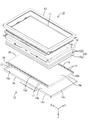
- FIG. 1 is an exploded perspective view showing a schematic configuration of a television receiver according to Embodiment 1 of the present invention.
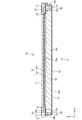
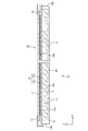
- the exploded perspective view which shows schematic structure of the liquid crystal display device with which a television receiver is equipped Sectional drawing which shows the cross-sectional structure along the short side direction of a liquid crystal display device Sectional drawing which shows the cross-sectional structure along the long side direction of a liquid crystal display device Sectional drawing which shows the cross-sectional structure of a liquid crystal panel roughly
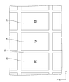
- the top view which shows the plane structure of the display area in the array substrate which comprises a liquid crystal panel
- the top view which shows the plane structure of the display area in CF substrate which comprises a liquid crystal panel
- Cross section of LED and LED board Graph showing excitation spectrum and emission spectrum in green phosphor used for LED
- Graph showing excitation spectrum and emission spectrum of red phosphor used in LED Sectional drawing which shows the structure of LED which concerns on the comparative example in a comparative experiment
- Graph showing excitation spectrum and emission spectrum of yellow phosphor used in LED Sectional drawing of LED which concerns on Embodiment 3 of this invention
- the disassembled perspective view of the liquid crystal display device which concerns on Embodiment 4 of this invention.
- FIGS. 1 A first embodiment of the present invention will be described with reference to FIGS.
- the liquid crystal display device 10 is illustrated.
- a part of each drawing shows an X axis, a Y axis, and a Z axis, and each axis direction is drawn to be a direction shown in each drawing.
- the upper side shown in FIG.3 and FIG.4 be a front side, and let the lower side of the figure be a back side.
- the television receiver TV includes a liquid crystal display device 10, front and back cabinets Ca and Cb that are accommodated so as to sandwich the liquid crystal display device 10, a power source P, a tuner T, And a stand S.
- the liquid crystal display device (display device) 10 has a horizontally long (longitudinal) rectangular shape (rectangular shape) as a whole and is accommodated in a vertically placed state.
- the liquid crystal display device 10 includes a liquid crystal panel 11 that is a display panel and a backlight device (illumination device) 12 that is an external light source, which are integrated by a frame-like bezel 13 or the like. Is supposed to be retained.
- the liquid crystal panel 11 includes a liquid crystal material, which is a substance whose optical characteristics change with application of an electric field, between a pair of transparent (translucent) glass substrates 20 and 21.
- the liquid crystal layer 22 is enclosed.
- the one disposed on the back side (backlight device 12 side) is the array substrate (substrate, active matrix substrate) 20, and is disposed on the front side (light emitting side).
- the substrate is a CF substrate (counter substrate) 21.
- a pair of front and back polarizing plates 23 are respectively attached to the outer surface sides of both the substrates 20 and 21.
- a TFT Thin Film Transistor
- a gate wiring 26 and a source wiring 27 forming a lattice shape are disposed so as to surround them.
- the pixel electrode 25 is made of a transparent conductive film such as ITO (Indium Tin Oxide). Both the gate wiring 26 and the source wiring 27 are made of a conductive material.
- the gate wiring 26 and the source wiring 27 are connected to the gate electrode 24a and the source electrode 24b of the TFT 24, respectively, and the pixel electrode 25 is connected to the drain electrode 24c of the TFT 24 via the drain wiring (not shown).
- the array substrate 20 is provided with a capacitor wiring (auxiliary capacitor wiring, storage capacitor wiring, Cs wiring) 33 that is parallel to the gate wiring 26 and overlaps the pixel electrode 25 in a plan view.
- the capacitor wiring 33 is arranged alternately with the gate wiring 26 in the Y-axis direction.
- the gate wiring 26 is disposed between the pixel electrodes 25 adjacent to each other in the Y-axis direction, whereas the capacitor wiring 33 is disposed at a position that substantially crosses the central portion of each pixel electrode 25 in the Y-axis direction.
- the end portion of the array substrate 20 is provided with a terminal portion routed from the gate wiring 26 and the capacitor wiring 33 and a terminal portion routed from the source wiring 27.
- Each signal or reference potential is input from an external circuit that is not to be operated, and the drive of the TFT 24 is thereby controlled.
- An alignment film 28 for aligning liquid crystal molecules contained in the liquid crystal layer 22 is formed on the inner surface side of the array substrate 20 (FIG. 5).
- each colored portion 29 has a vertically long rectangular shape in plan view following the outer shape of the pixel electrode 25.
- each coloring part 29 which comprises a color filter
- the light-shielding part (black matrix) 30 which makes the grid
- the light shielding portion 30 is disposed so as to overlap with the gate wiring 26, the source wiring 27, and the capacitor wiring 33 on the array substrate 20 in plan view.
- a counter electrode 31 is provided on the surface of each colored portion 29 and the light shielding portion 30 so as to face the pixel electrode 25 on the array substrate 20 side.
- An alignment film 32 for aligning liquid crystal molecules contained in the liquid crystal layer 22 is formed on the inner surface side of the CF substrate 21.
- the backlight device 12 includes a chassis 14 having a substantially box shape having an opening 14 c that opens to the front side, that is, the light emitting side (the liquid crystal panel 11 side), and an opening 14 c of the chassis 14.
- An optical member 15 arranged in a covering manner and a frame 16 for pressing a light guide member 19 described below from the front side are provided.
- the light guide member 19 that leads to the light emission side) is accommodated.
- the backlight device 12 includes LED substrates 18 having LEDs 17 at both ends on the long side, and a light guide member 19 at the center between the LED substrates 18 disposed on both ends. Is a so-called edge light type (side light type). Below, each component of the backlight apparatus 12 is demonstrated in detail.
- the chassis 14 is made of a metal plate such as an aluminum plate or an electrogalvanized steel plate (SECC), for example, and as shown in FIGS. 2 to 4, a bottom plate 14a having a horizontally long rectangular shape similar to the liquid crystal panel 11, and a bottom plate It consists of the side plate 14b which stands
- the long side direction of the chassis 14 (bottom plate 14a) coincides with the X-axis direction (horizontal direction), and the short side direction coincides with the Y-axis direction (vertical direction). Further, the frame 16 and the bezel 13 can be screwed to the side plate 14b.
- SECC electrogalvanized steel plate
- the optical member 15 has a horizontally long rectangular shape when viewed in a plane, like the liquid crystal panel 11 and the chassis 14.
- the optical member 15 is placed on the front side (light emission side) of the light guide member 19 and is disposed between the liquid crystal panel 11 and the light guide member 19 so as to emit light from the light guide member 19.
- the transmitted light is emitted toward the liquid crystal panel 11 while giving a predetermined optical action to the transmitted light.
- the optical member 15 includes a diffusion plate 15a disposed on the back side (light guide member 19 side, opposite to the light emitting side) and an optical sheet 15b disposed on the front side (liquid crystal panel 11 side, light emitting side). Composed.
- the diffusion plate 15a has a structure in which a large number of diffusion particles are dispersed in a substantially transparent synthetic resin base material having a predetermined thickness and has a function of diffusing transmitted light.
- the optical sheet 15b has a sheet shape that is thinner than the diffusion plate 15a, and three optical sheets 15b are laminated (FIG. 2). Specific types of the optical sheet 15b include, for example, a diffusion sheet, a lens sheet, a reflective polarizing sheet, and the like, which can be appropriately selected and used. In FIGS. 3 and 4, for convenience, the three optical sheets 15b are simplified to one.
- the frame 16 is formed in a frame shape (frame shape) extending along the outer peripheral end portion of the light guide member 19, and the outer peripheral end portion of the light guide member 19 extends over substantially the entire circumference. It can be pressed from the front side.
- the frame 16 is made of a synthetic resin and has a light shielding property by having a surface with, for example, a black color.
- first reflective sheets R ⁇ b> 1 that reflect light are respectively formed on the back side surfaces of the long side portions of the frame 16, that is, the surfaces facing the light guide member 19 and the LED substrate 18 (LED 17). It is attached.
- the first reflection sheet R1 has a size extending over almost the entire length of the long side portion of the frame 16, and is in direct contact with the end portion of the light guide member 19 that faces the LED 17 and also guides the light.
- the end portion of the member 19 and the LED substrate 18 are collectively covered from the front side. Further, the frame 16 can receive the outer peripheral end of the liquid crystal panel 11 from the back side.
- the LED 17 is a so-called top type in which the LED 17 is surface-mounted and its light emitting surface 17a faces away from the LED substrate 18 side.
- the detailed configuration of the LED 17 will be described later in detail.
- the LED substrate 18 is made of a synthetic resin (glass epoxy resin or the like) having a white surface with excellent light reflectivity, and as shown in FIG. 2, the long side direction of the chassis 14 (the LED 17 side in the light guide member 19).
- the X-axis direction and a posture in which the plate surface is parallel to the X-axis direction and the Z-axis direction, that is, the liquid crystal panel 11 and the light guide member 19. It is accommodated in the chassis 14 in a posture orthogonal to the plate surface of the (translucent optical member 15).
- the LED substrate 18 has a posture in which the long side direction on the plate surface coincides with the X-axis direction, the short side direction coincides with the Z-axis direction, and the plate thickness direction orthogonal to the plate surface coincides with the Y-axis direction. It is said.
- the LED substrate 18 is arranged in a pair at a position sandwiching the light guide member 19 in the Y-axis direction. Specifically, the long side of the light guide member 19 and the chassis 14 is arranged. Each side plate 14b is interposed so as to be accommodated from the front side with respect to the chassis 14 along the Z-axis direction. A plurality (27 in FIG. 5) of LEDs 17 are provided on the inner side, that is, the surface facing the light guide member 19 side (the surface facing the light guide member 19) of the LED substrate 18.
- the LEDs 17 are arranged intermittently in parallel along the side direction (long side direction of the translucent optical member 15 and the X-axis direction), and an LED group is configured by the LEDs 17 arranged in parallel in this line.
- Each LED 17 is surface-mounted on the surface of the LED substrate 18 facing the light guide member 19 side, and this is the mounting surface.
- the terminal portions formed at both ends of the wiring pattern are connected to an external driving circuit, so that driving power can be supplied to each LED 17.
- the LED substrate 18 is a single-sided mounting type in which only one side of the plate surface is a mounting surface.
- the interval between the LEDs 17 adjacent to each other in the X-axis direction, that is, the arrangement pitch of the LEDs 17 is substantially equal.
- Each LED board 18 is attached such that the plate surface opposite to the mounting surface is in contact with the inner surface of each side plate 14 b on the long side of the chassis 14. Accordingly, the light emitting surfaces 17a of the LEDs 17 mounted on the LED substrates 18 are opposed to each other, and the optical axes of the LEDs 17 substantially coincide with the Y-axis direction.
- a raw material used for the LED board 18 it is also possible to set it as the structure which used metal materials, such as the same aluminum-type material as the chassis 14, for example, and formed the wiring pattern through the insulating layer on the surface.
- the light guide member 19 is made of a synthetic resin material (for example, acrylic or the like) having a refractive index sufficiently higher than that of air and substantially transparent (excellent translucency). As shown in FIG. 2, the light guide member 19 is formed in a plate shape that is horizontally long when viewed in a plane, like the liquid crystal panel 11 and the chassis 14, and the long side direction on the plate surface is the X-axis direction. In addition, the short side direction coincides with the Y-axis direction, and the plate thickness direction orthogonal to the plate surface coincides with the Z-axis direction. As shown in FIG.
- the light guide member 19 is disposed in the chassis 14 immediately below the liquid crystal panel 11 and the optical member 15, and forms a pair of LEDs disposed at both ends of the long side of the chassis 14. They are arranged between the substrates 18 so as to be sandwiched in the Y-axis direction. Therefore, the alignment direction of the LED 17 (LED substrate 18) and the light guide member 19 coincides with the Y-axis direction, whereas the alignment direction of the optical member 15 (liquid crystal panel 11) and the light guide member 19 is the Z-axis direction. And the arrangement directions of the two are orthogonal to each other.
- the light guide member 19 introduces light emitted from the LED 17 in the Y-axis direction, and rises toward the optical member 15 side (front side, light emission side) while propagating the light inside. It has a function to emit light. Since the light guide member 19 is disposed at the center position in the short side direction of the bottom plate 14a of the chassis 14, it can be said that the light guide member 19 is supported from the back side by the center portion in the short side direction of the bottom plate 14a.
- the light guide member 19 is formed to be slightly larger than the optical member 15 described above, and its outer peripheral end projects outward from the outer peripheral end surface of the optical member 15 and is pressed by the frame 16 described above. (FIG. 3).
- the light guide member 19 has a substantially flat plate shape extending along each plate surface of the bottom plate 14 a of the chassis 14 and the optical member 15, and the plate surface is in the X-axis direction. And parallel to the Y-axis direction.
- the surface facing the front side is a light emitting surface 19 a that emits internal light toward the optical member 15 and the liquid crystal panel 11.
- both end surfaces on the long side that are long along the X-axis direction are respectively LED 17 (LED substrate 18) and LED 17, as shown in FIG.
- the first reflection sheet R1 described above is arranged on the front side of the space held between the LED 17 and the light incident surface 19b, whereas the first reflection sheet R1 is arranged on the back side of the space.
- the second reflection sheet R2 is arranged so as to sandwich the same space therebetween. Both reflection sheets R1 and R2 are arranged so as to sandwich the LED 17 side end portion of the light guide member 19 and the LED 17 in addition to the space. Thereby, the light from LED17 can be made to inject efficiently with respect to the light-incidence surface 19b by repeatedly reflecting between both reflection sheet R1, R2.
- the light incident surface 19b is a surface that is parallel to the X-axis direction and the Z-axis direction, and is a surface that is substantially orthogonal to the light emitting surface 19a. Further, the alignment direction of the LED 17 and the light incident surface 19b coincides with the Y-axis direction and is parallel to the light emitting surface 19a.
- the surface 19c opposite to the light exit surface 19a reflects the light in the light guide member 19 and rises to the front side as shown in FIGS.
- a third reflective sheet R3 capable of covering the entire area is provided.
- the third reflection sheet R ⁇ b> 3 is disposed between the bottom plate 14 a of the chassis 14 and the light guide member 19.
- a scattering portion (not shown) that scatters the light in the light guide member 19 is provided on at least one of the light exit surface 19a and the opposite surface 19c of the light guide member 19 or on the surface of the third reflection sheet R3.
- the like are patterned so as to have a predetermined in-plane distribution, whereby the light emitted from the light emitting surface 19a is controlled to have a uniform distribution in the surface.
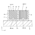
- the LED 17 includes an LED element (LED chip, light emitting element) 40 that is a light source and a sealing material (translucent material) that contains a phosphor that emits light when excited by light from the LED element 40.
- LED element LED chip, light emitting element
- sealing material transparent material
- the emitted light emitted from the light emission surface 17a is made into substantially white light as a whole.
- the components of the LED 17 will be sequentially described in detail with reference to FIG.
- the LED element 40 is a semiconductor made of, for example, an InGaN-based material, and emits light when a voltage is applied in the forward direction.
- the LED element 40 has a main emission wavelength in the emitted light in a blue wavelength region (about 420 nm to about 480 nm), and can be said to be a blue LED element that emits blue light in a single color.
- the main emission wavelength of the LED element 40 is more preferably in the range of 440 nm to 460 nm, and specifically, for example, 451 nm.
- the LED element 40 is connected to a wiring pattern on the LED substrate 18 disposed outside the case 42 by a lead frame (not shown).
- the sealing material 41 is made of a substantially transparent thermosetting resin material, specifically, an epoxy resin material, a silicone resin material, or the like. In the manufacturing process of the LED 17, the sealing material 41 fills the internal space of the case 42 in which the LED element 40 is accommodated, thereby sealing the LED element 40 and the lead frame and protecting them. .
- the encapsulant 41 contains a phosphor described below in a dispersed manner, and functions as a dispersion medium (binder) that holds the phosphor.
- the phosphor emits light existing in a predetermined wavelength region by being excited by light (blue light) from the LED element 40.
- emitted light fluorescence
- the main emission wavelengths are different from each other (a first phosphor and a second phosphor described below) are used.
- the first phosphor is a green phosphor that emits light whose main emission wavelength is in the green wavelength region (about 500 nm to about 570 nm) when excited by the light from the LED element 40.
- the second phosphor is a red phosphor that emits light having a main emission wavelength in a red wavelength region (about 600 nm to about 780 nm) by being excited by light from the LED element 40.
- the LED 17 includes blue light (blue component light) emitted from the LED element 40, green light (green component light) emitted from the green phosphor as the first phosphor, and the second phosphor.
- white light can be emitted by red light (red component light) emitted from the red phosphor.
- red component light red component light
- green light and The emission intensity in red light can be increased, which is excellent in terms of color rendering in the emitted light.
- the chromaticity of the emitted light in the LED 17 changes according to the absolute value or relative value of the content in the green phosphor and the red phosphor, for example, the content of the green phosphor and the red phosphor is changed. It is possible to adjust the chromaticity of the emitted light in the LED 17 by appropriately adjusting.
- ⁇ -SiAlON which is a kind of sialon phosphor
- the sialon-based phosphor is a substance in which a part of silicon atoms of silicon nitride is replaced with aluminum atoms and a part of nitrogen atoms with oxygen atoms, that is, a nitride.
- a sialon-based phosphor that is a nitride is superior in luminous efficiency and durability as compared with other phosphors made of, for example, sulfides or oxides.
- ⁇ -SiAlON which is a kind of sialon-based phosphor, has a general formula Si6-zAlzOzN8-z: Eu (z indicates a solid solution amount) or (Si, Al) in which aluminum and oxygen are dissolved in ⁇ -type silicon nitride crystal. ) 6 (O, N) 8: A substance represented by Eu.
- ⁇ -SiAlON for example, Eu (europium) is used as an activator, and thereby the color purity of green light, which is emitted light, is particularly high.
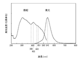
- ⁇ -SiAlON which is the green phosphor according to the present embodiment, has a main emission wavelength of the emitted light of, for example, about 540 nm (see FIG. 9).
- casoon which is a kind of cascading phosphor.
- Cousin-based phosphors are nitrides containing calcium atoms (Ca), aluminum atoms (Al), silicon atoms (Si), and nitrogen atoms (N).
- Ca calcium atoms
- Al aluminum atoms
- Si silicon atoms
- N nitrogen atoms
- other phosphors made of sulfides, oxides, etc.
- the cascading phosphor uses rare earth elements (for example, Tb, Yg, Ag, etc.) as an activator.
- Casun which is a kind of cousin phosphor, uses Eu (europium) as an activator and is represented by the composition formula CaAlSiN3: Eu.
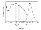
- the main emission wavelength of the emitted light of the red phosphor according to the present embodiment is about 650 nm (see FIG. 10).
- the case 42 is made of a synthetic resin material (for example, a polyamide-based resin material) or a ceramic material having a white surface with excellent light reflectivity.
- the case 42 has a substantially box shape having an opening 42c on the light emitting side (light emitting surface 17a side, opposite to the LED substrate 18 side) as a whole, and roughly along the mounting surface of the LED substrate 18. It has a bottom wall part 42a that extends and a side wall part 42b that rises from the outer edge of the bottom wall part 42a.
- the bottom wall portion 42a has a rectangular shape when viewed from the light emitting side
- the side wall portion 42b has a substantially rectangular tube shape along the outer peripheral edge of the bottom wall portion 42a, and from the light emitting side.
- the LED element 40 is disposed on the inner surface (bottom surface) of the bottom wall portion 42 a constituting the case 42.
- a lead frame is passed through the side wall portion 42b.
- an end portion arranged in the case 42 is connected to the LED element 40, whereas an end portion led out of the case 42 is connected to the wiring pattern of the LED substrate 18.
- the excitation spectrum and emission spectrum in the two types of phosphors included in the LED 17 will be described.
- the excitation spectrum and emission spectrum of the green phosphor (first phosphor) are as shown in FIG. 9, and the excitation spectrum and emission spectrum of the red phosphor (second phosphor) are as shown in FIG.
- the excitation spectrum in the green phosphor is a wavelength region covering the wavelength region of near ultraviolet rays, purple (blue light), and green (part of the short wavelength side) of visible light.
- the emission spectrum includes the entire green wavelength region (including slightly blue and yellow wavelength regions), and the main emission wavelength is about 540 nm. Explaining the latter, as shown in FIG.
- the excitation spectrum of the red phosphor is a wavelength region covering the wavelength region of near ultraviolet rays, the visible light purple, blue, green, and yellow (part of the short wavelength side).
- the emission spectrum includes the entire red wavelength region (including slightly green and yellow wavelength regions), and the main emission wavelength is about 650 nm.
- the green phosphor hardly absorbs red light emitted from the red phosphor as excitation light, but the red phosphor has a property of absorbing green light emitted from the green phosphor to some extent as excitation light. I can say that. This is apparent from the fact that the excitation spectrum of the red phosphor in FIG. 10 includes the main emission wavelength of 540 nm of the green phosphor.
- the LED 17 according to the present embodiment employs a configuration in which two types of phosphors having different main emission wavelengths in the emitted light are arranged unevenly in the LED 17. That is, for each of the two types of phosphors, a dedicated sealing material 41 is prepared for each type, and each phosphor is associated with one type of the dedicated sealing material 41 (one-to-one correspondence). In other words, since each of them is dispersed and blended, different kinds of phosphors in the sealing material 41 are not mixed. Then, two kinds of sealing materials 41 containing different phosphors are filled so as to be unevenly distributed in different regions in the internal space of the case 42.
- the sealing material 41 includes a green sealing material (first sealing material) 41G containing only a green phosphor (first phosphor) of two types of phosphors, and a red phosphor (first phosphor). There are two types of red sealing material (second sealing material) 41R containing only two phosphors.
- the suffix G is added to the code of the green sealing material containing only the green phosphor, and the suffix is added to the code of the red sealing material containing only the red phosphor.
- R is added and generically referred to without distinction, no suffix is added to the reference sign.
- the case 42 is provided with the partition wall portion 43 that divides the internal space into the two partition spaces S1 and S2. It has been.
- the partition wall 43 is formed integrally with the case 42 and is configured to rise from the bottom wall 42a along the side wall 42b.
- the partition wall portion 43 is disposed at the center position in the X-axis direction of the bottom wall portion 42a and has a flat plate shape having plate surfaces along the Y-axis direction and the Z-axis direction. That is, the partition wall 43 partitions the internal space of the case 42 at substantially equal intervals in the X-axis direction, and the pair of partition spaces S1 and S2 arranged side by side in the X-axis direction have substantially the same volume. Has been.
- the rising height from the bottom wall portion 42a of the partition wall portion 43 is substantially equal to the total height of the case 42, and the rising tip portion reaches the opening 42c.
- the rising end surface of the partition wall portion 43 is flush with the front end surface of the side wall portion 42 b and the light emitting surface 17 a of the LED 17.
- the two types of sealing materials 41G and 41R described above are filled individually (corresponding to one to one) into the two partitioned spaces S1 and S2 in the case 42 for each type.
- the first partition space S1 on the left side shown in FIG. 8 is filled with only the green sealing material 41G
- the second partition space S2 on the right side of FIG. Only the material 41R is filled.
- the green sealing material 41G and the red sealing material 41R are unevenly distributed left and right in the X-axis direction.
- the LED elements 40 are individually arranged in the two partitioned spaces S1 and S2 in the case 42, respectively.
- the LED element 40 is sealed with a green sealing material (first sealing material) 41G, and supplies green light to only the green phosphor (first LED element).
- a red LED element (second LED element) 41R which is sealed by a red sealing material (second sealing material) 41R and supplies excitation light only to the red phosphor.
- the red LED element sealed with the red sealing material 41R is used with the suffix G added to the code of the green LED element sealed with the green sealing material 41G.
- the suffix is not added to the reference sign.
- the following comparative experiment was performed.
- the LED 17CO according to the comparative example has a configuration in which a case 40CO is filled with a sealing material 41CO in which a green phosphor and a red phosphor similar to those in the above-described embodiment are randomly dispersed and blended. Is done.
- the LED element 40CO and the case 42CO have substantially the same structure as that described in the present embodiment, except that the case 42CO does not have a partition wall that is one of the features of the present embodiment. It is said that.
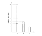
- FIG. 12 shows the emission intensity of blue light and green light when the LED element 40CO emits light with a predetermined emission intensity. Measurement was performed (FIG. 12).
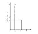
- FIG. 13 shows a graph summarizing changes in the emission intensity of light of each color obtained in the first and second stage experiments. In the graphs shown in FIG.
- the emission intensity of the emitted light in the LED element 40CO as the emission source is a reference value “16”, and the emission intensity of each color light in the emitted light of the LED 17CO is relative to the reference value. It is written as a relative value.
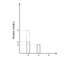
- the blue light and the green light of the emitted light when only the green LED element 40G arranged in the first partitioned space S1 of the LED 17 is turned on (the red LED element 40R is turned off).
- the light emission intensity was measured (FIG. 15).
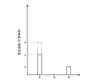
- the emission intensity of the emitted blue light and red light when only the red LED element 40R disposed in the second section space S2 of the LED 17 is turned on (the green LED element 40G is turned off). was measured (FIG. 16).
- the emission intensity of the emitted blue light, green light, and red light when the two LED elements 40G and 40R were both turned on was measured (FIG. 17).
- the emission intensity of the emitted light from each of the LED elements 40G and 40R as the emission source is set to the reference value “8”, and the emission intensity of the light of each color in the emitted light from the LED 17 is as follows. It is described as a relative value with respect to the reference value. Further, in the embodiment, there are two LED elements 40G and 40R, and the number of the LED elements 40G and 40R is twice as large as that of the comparative example. And half of it.
- the green phosphor absorbs about half of the blue light (specifically, about “8”) from the LED element 40CO, and the emission intensity (specifically, about "6") emits green light. Therefore, the luminous efficiency of the green phosphor with respect to blue excitation light is about 75%.
- the red phosphor absorbs a predetermined amount (specifically, about “3”) of the blue light from the LED element 40CO and also the green light from the green phosphor. By absorbing a predetermined amount (specifically, about “3”), the emission intensity (specifically, less than the absorption amount of blue excitation light and green excitation light (specifically, about “6”)).
- the luminous efficiency of the red phosphor with respect to blue excitation light and green excitation light is about 50%. Specifically, the emission efficiency of the red phosphor with respect to blue excitation light is about 67%, whereas the emission efficiency of the red phosphor with respect to green excitation light is about 33%. .
- the luminous efficiency of the entire LED 17CO is such that the blue light and green light in the emitted light of the LED 17CO with respect to the reference value (specifically “16”) of the emitted light intensity of the emitted light in the LED element 40CO.
- the red light intensity can be represented by the sum of the emission intensities (specifically, “11”), and the value is about 69%.
- the green phosphor absorbs about half (specifically, about “4”) of blue light from the green LED element 40G as the first LED element, and more than the absorbed amount. It emits green light with low emission intensity (specifically, about “3”). Accordingly, the luminous efficiency of the green phosphor with respect to the blue excitation light is about 75% as in the comparative example.
- the red phosphor absorbs a predetermined amount (specifically, about “3”) of blue light from the red LED element 40R, which is the second LED element, and the amount of absorption. It emits red light with a lower emission intensity (specifically, about “2”).
- the luminous efficiency of the red phosphor with respect to blue excitation light is about 67%.
- the light emission efficiency of the entire LED 17 is the output efficiency of the LED 17 with respect to a reference value (specifically “16”) obtained by adding the light emission intensities of the two LED elements 40G and 40R. It can be represented by the magnitude (specifically “14”) of the emission intensity of blue light, green light and red light in the incident light, and the value is about 88%.
- the LED 17 according to the example has higher luminous efficiency than the LED 17CO according to the comparative example.
- This is mainly due to the fact that the red phosphor absorbs green light from the green phosphor in the comparative example. That is, the green light absorbed by the red phosphor is emitted from the green phosphor by absorbing the blue light from the LED element 40CO, and the red light emitted from the red phosphor does not emit or emit light.
- processes that have passed through two stages include losses at each stage (light conversion efficiency is poor).
- the luminous efficiency of the red phosphor with respect to the green excitation light is remarkably low (about 50%), which is considered to be a cause of further reducing the luminous efficiency of the entire LED 17CO.
- the green sealing material 41G containing the green phosphor and the red sealing material 41R containing the red phosphor are the case 42.
- the green light emitted from the green phosphor is unevenly distributed in the case 42.
- the light is reflected or absorbed by the partition wall 43 and hardly enters the adjacent second partition space S ⁇ b> 2 and is exclusively emitted from the opening 42 c of the case 42.
- the green light emitted from the green phosphor is hardly absorbed by the red phosphor. Therefore, it can be said that the emitted light from the green phosphor and the red phosphor is one in which only one stage of the excitation / emission process has passed, and is excellent in light conversion efficiency.
- the LED 17 according to the example has higher utilization efficiency and light emission efficiency of blue light from the LED elements 40G and 40R which are light emission sources than the comparative example.
- the color rendering property in the backlight apparatus 12 can be improved, and the improvement of a brightness
- the LED 17 according to the embodiment for the liquid crystal display device 10 the display quality of the display image in the liquid crystal display device 10 can be improved, and the luminance can be improved or the power consumption can be reduced.
- the LED (light source) 17 of the present embodiment emits light when excited by the light from the LED element (light emitting element) 40 and the LED element 40, and the main emission wavelength in the emitted light.
- the LED element (light emitting element) 40 and the LED element 40 are provided with a plurality of types of phosphors that are different from each other and a case (container) 42 in which the LED element 40 is accommodated and the plurality of types of phosphors are unevenly distributed in the internal space.
- the color rendering properties related to the emitted light of the LED 17 are excellent.
- the LED element 40 has Light emitted from each phosphor when excited by light is hardly absorbed by a phosphor of a different type from the light emitting source. Thereby, the light emitted from a plurality of types of phosphors can be used effectively as the emitted light of the LED 17 with low loss, and the luminous efficiency can be increased.
- a partition wall portion 43 that partitions the internal space of the case 42 into a plurality of partition spaces S1 and S2 in which a plurality of types of phosphors are associated with each other is provided.
- the internal space of the case 42 is divided into a plurality of divided spaces S1 and S2 by the divided wall portion 43, and is emitted from the respective phosphors associated with the divided spaces S1 and S2.
- the light is prevented from entering the divided spaces S2 and S1 different from the divided spaces S1 and S2 in which the phosphors of the light emitting sources exist, and is different from the light emitting sources existing in the other divided spaces S2 and S1. It is prevented from being absorbed by the phosphor. Thereby, the light emitted from each phosphor can be utilized with lower loss, and the luminous efficiency can be further increased.
- a plurality of types of phosphors are individually present for each type in each of the plurality of partitioned spaces S1, S2.
- each partition space S1, S2 and the type of phosphor are associated one-to-one, the light emitted from each phosphor in each partition space S1, S2 is the light source. It can be surely prevented from being absorbed by another type of phosphor. Thereby, the light emitted from each phosphor can be utilized with even lower loss, and the luminous efficiency can be further increased.
- the LED elements 40 are individually arranged in each of the plurality of partitioned spaces S1, S2. If it does in this way, it will become possible to control the output of each LED element 40 corresponding to each division space S1 and S2. This is useful for adjusting the color and brightness of the light emitted from the LED 17.
- the same thing is used for the LED element 40 distribute
- the partition wall 43 is formed integrally with the case 42. In this way, as compared with the case where the partition wall portion is a separate part from the case 42, it is possible to reduce the number of assembling steps at the time of manufacture, which is suitable for reducing the manufacturing cost.
- the case 42 is formed with an opening 42c for emitting light from the LED element 40 and the phosphor, and the partition wall 43 has a height to reach the opening 42c.
- the partition wall 43 since the partition wall 43 has a height that reaches the opening 42c, it is different from the light emitting source until the light from each phosphor is emitted from the opening 42c. It can prevent more reliably that it is absorbed by the kind of fluorescent substance.
- partition wall 43 is arranged so as to partition the internal space of the case 42 at substantially equal intervals. In this way, the volumes of the divided spaces S1, S2 in which the respective phosphors are arranged can be made substantially equal.
- a plurality of sealing materials (translucent resin materials) 41 containing a phosphor are provided, and the plurality of sealing materials 41 are filled so as to be unevenly distributed in different regions in the internal space of the case 42. Yes. In this way, since the phosphor is contained in the sealing material 41 filled in the case 42, a plurality of types of phosphors can be easily unevenly distributed in the case 42.
- the plurality of sealing materials 41 individually contain a plurality of types of phosphors for each type. In this way, since each sealing material 41 and the type of phosphor are associated one-to-one, a plurality of types of phosphors are mixed in one of the plurality of sealing materials. Compared with the case where a sealing material is included, the light emitted from each phosphor is less likely to be absorbed by a different type of phosphor from the light emitting source. Thereby, the light emitted from each phosphor can be used as the emitted light with a lower loss, and the luminous efficiency can be further increased.
- the LED element 40 is a blue LED element 40 in which the main emission wavelength in the emitted light is in the blue wavelength region, whereas the plurality of types of phosphors have a wavelength region in which the main emission wavelength in the emitted light is green. And a red phosphor in which the main emission wavelength of the emitted light is in the red wavelength region. In this way, substantially white light excellent in color rendering can be emitted as a whole by the blue light from the blue LED element 40, the green light from the green phosphor, and the red light from the red phosphor. it can.
- the light emitting element is the LED element 40. In this way, low power consumption and long life are achieved.
- Embodiment 2 A second embodiment of the present invention will be described with reference to FIG. 18 or FIG.
- the LED 117 is divided into three internal spaces and a yellow phosphor is added.
- the case 142 is provided with a pair of partition wall portions 143 so that the internal space is partitioned into three partition spaces S1 to S3.
- the three partitioned spaces S1 to S3 are defined as a first partitioned space S1, a second partitioned space S2, and a third partitioned space S3 in order from the left side shown in FIG.
- the first partition space S1 is filled with a green sealing material 141G containing only a green phosphor
- the third sealing space S3 is filled with a red sealing material 141R containing only a red phosphor.
- the second section space S2 is filled with a yellow sealing material (third sealing material) 141Y containing only a yellow phosphor (third phosphor).
- a yellow sealing material third sealing material
- the same LED elements 140 that emit blue monochromatic light are individually accommodated in the same manner as in the first embodiment, and are accommodated in the first partitioned space S1.
- the blue LED element 140G is housed in the second partitioned space S2, and the yellow LED element 140Y is housed in the third partitioned space S3.
- the red LED element 140R is housed in the third partitioned space S3.
- the yellow phosphor will be described in detail.
- the yellow phosphor is excited by light (blue light) from the LED element 140 to emit light having a main emission wavelength in a yellow wavelength region (about 570 nm to about 600 nm).
- ⁇ -SiAlON which is a kind of SiAlON phosphor that is a nitride, is preferably used.
- yellow light can be emitted with high efficiency compared with the case where a phosphor made of sulfide or oxide is used, for example.
- ⁇ -SiAlON uses Eu (europium) as an activator, and has a general formula Mx (Si, Al) 12 (O, N) 16: Eu (M is a metal ion, x is a solid solution amount) Respectively).
- M is a metal ion
- x is a solid solution amount
- Ca is a metal ion
- Ca is a solid solution amount
- the excitation spectrum and emission spectrum in the yellow phosphor are as shown in FIG. As shown in FIG. 19, the excitation spectrum in the yellow phosphor includes a wavelength region ranging from near-ultraviolet wavelength, visible light purple, blue, and green, and the emission spectrum includes the entire yellow wavelength region.
- the yellow phosphor can absorb green light emitted from the green phosphor to some extent as excitation light. This is apparent from the fact that the excitation spectrum of the yellow phosphor in FIG. 19 includes 540 nm, which is the main emission wavelength of the green phosphor. Further, the red phosphor can absorb the yellow light emitted from the yellow phosphor together with the green light emitted from the green phosphor to some extent as excitation light, and this indicates that the excitation spectrum in FIG. 10 includes 580 nm. You can see from that.
- the LED 117 according to the present embodiment includes a yellow phosphor in addition to the red phosphor and the green phosphor. Therefore, compared with the LED 17 described in the first embodiment, the emission intensity in yellow light. Therefore, the color rendering property of the emitted light is further improved.
- the LED 117 can emit substantially white light as a whole by adjusting the content and concentration of each phosphor or adjusting the light emission intensity of each LED element 140G, 140Y, 140R. it can.
- the LED 117 includes three types of sealing materials 141G, 141Y, and 141R that individually contain three types of phosphors having different main emission wavelengths of emitted light for each type.
- the light emitted from each phosphor is reliably prevented from being absorbed by a phosphor other than the light emitting source. Specifically, the green light emitted from the green phosphor is prevented from being absorbed by the yellow phosphor and the red phosphor, and the yellow light emitted from the yellow phosphor is absorbed by the red phosphor. Being prevented. Thereby, the emitted light from each phosphor can be effectively used as the emitted light of the LED 117, and the luminous efficiency of the LED 117 can be increased.
- the plurality of types of phosphors include yellow phosphors whose main emission wavelength in the emitted light is in the yellow wavelength region. If it does in this way, color rendering property can be improved further by adding yellow fluorescent substance to green fluorescent substance and red fluorescent substance as fluorescent substance.
- the LED 217 includes a green encapsulant 241G containing a green phosphor and a red encapsulant containing a red phosphor in three partitioned spaces S1 to S3 in the case 242.
- the stopping material 241R and the transparent sealing material 241T that does not contain the phosphor are respectively filled.
- the first partitioned space S1 is filled with the transparent sealing material 241T and accommodates the transparent LED element 240T.
- the second partition space S2 is filled with a green sealing material 241G and accommodates a green LED element 240G.
- the third section space S3 is filled with a red sealing material 241R and accommodates a red LED element 240R.
- the transparent sealing material 241T is made of a substantially transparent thermosetting resin material and does not contain any phosphor, so that the blue monochromatic light emitted from the transparent LED element 240T is hardly lost. Can be emitted. Thereby, it is possible to further increase the color purity of the blue light in the light emitted from the LED 217.
- the same LED elements 240 are used as in the second embodiment.
- the liquid crystal display device 310 has a configuration in which a liquid crystal panel 311 and a direct backlight device 312 are integrated by a bezel 313 or the like. Note that the configuration of the liquid crystal panel 311 is the same as that of the above-described first embodiment, and thus redundant description is omitted. Hereinafter, the configuration of the direct type backlight device 312 will be described.
- the backlight device 312 is arranged so as to cover a substantially box-shaped chassis 314 having an opening 314c on the light emitting side (liquid crystal panel 311 side) and the opening 314c of the chassis 314. And an optical member 315 arranged along the outer edge of the chassis 314 and a frame 316 that holds the outer edge of the optical member 315 between the chassis 314 and the frame 316.
- an LED 317 disposed in an opposing manner at a position directly below the optical member 315 (liquid crystal panel 311), an LED substrate 318 on which the LED 317 is mounted, and a position corresponding to the LED 317 in the LED substrate 318
- a substrate holding member 45 for holding the LED substrate 318 in an attached state with respect to the chassis 314.
- a reflection sheet 46 that reflects the light in the chassis 314 toward the optical member 315 is provided in the chassis 314.
- the backlight device 312 since the backlight device 312 according to the present embodiment is a direct type, the light guide member 19 used in the edge light type backlight device 12 illustrated in the first embodiment is not provided.
- the configuration of the frame 316 is the same as that of the first embodiment except that the first reflective sheet R1 is not provided, and thus the description thereof is omitted. Next, each component of the backlight device 312 will be described in detail.
- the chassis 314 is made of metal, and as shown in FIGS. 21 and 22, a bottom plate 314a that has a horizontally long rectangular shape like the liquid crystal panel 311, and a front side (light emitting side) from the outer end of each side of the bottom plate 314a. ) And a receiving plate 47 projecting outward from the rising end of each side plate 314b, and as a whole, has a shallow substantially box shape opened toward the front side.
- the long side direction of the chassis 314 matches the X-axis direction (horizontal direction), and the short side direction matches the Y-axis direction (vertical direction).
- a frame 316 and an optical member 315 to be described below can be placed on each receiving plate 47 in the chassis 314 from the front side.
- a frame 316 is screwed to each receiving plate 47.
- the bottom plate 314a of the chassis 314 is provided with attachment holes for attaching the substrate holding members 45, respectively.
- the optical member 315 is composed of a diffusion plate 315a and two optical sheets 315b.
- the LED substrate 318 on which the LEDs 317 are mounted will be described.
- the LED substrate 318 has a base material that is horizontally long when viewed in a plane, and the inside of the chassis 314 is in a state where the long side direction coincides with the X-axis direction and the short side direction coincides with the Y-axis direction. Are accommodated while extending along the bottom plate 314a.
- the LED 317 is surface-mounted on the surface facing the front side (the surface facing the optical member 315 side) among the plate surfaces of the base material of the LED substrate 318.
- the LED 317 has a light emitting surface facing the optical member 315 (the liquid crystal panel 311) and an optical axis that coincides with the Z-axis direction, that is, the direction orthogonal to the display surface of the liquid crystal panel 311.
- the LEDs 317 are arranged in parallel in a matrix along the long side direction (X-axis direction) and the short side direction (Y-axis direction) on the plate surface of the LED substrate 318, and a predetermined wiring pattern (see FIG. Are not connected to each other.
- the diffusion lens 44 is made of a synthetic resin material (for example, polycarbonate, acrylic, etc.) that is substantially transparent (having high translucency) and has a refractive index higher than that of air.
- the diffusing lens 44 has a predetermined thickness and is formed in a substantially circular shape when seen in a plan view, and covers each LED 317 individually from the front side with respect to the LED substrate 318, that is, overlaps with each LED 317 when seen in a plan view. Each is attached to do.
- the diffusion lens 44 can emit light having a strong directivity emitted from the LED 317 while diffusing it.
- the diffusion lens 44 is disposed at a position that is substantially concentric with the LED 317 when seen in a plan view.
- the substrate holding member 45 is made of a synthetic resin such as polycarbonate and has a white surface with excellent light reflectivity.
- the substrate holding member 45 includes a main body portion along the plate surface of the LED substrate 318 and a fixing portion that protrudes from the main body portion to the back side, that is, the chassis 314 side and is fixed to the chassis 314.
- the pair of substrate holding members 45 arranged on the center side of the screen is provided with a support portion that protrudes from the main body portion to the front side, and the optical member 315 is provided from the back side by this support portion. It is possible to support.
- the reflection sheet 46 has a size covering the inner surface of the chassis 314 over almost the entire area.
- the reflection sheet 46 can reflect the light in the chassis 314 toward the optical member 315 side.
- the reflection sheet 46 extends along the bottom plate 314a of the chassis 314 and covers a large portion of the bottom plate 314a.
- the reflection sheet 46 rises from each outer end of the bottom portion 46a to the front side and is inclined with respect to the bottom portion 46a.
- the four rising portions 46b and the extending portions 46c that extend outward from the outer ends of the rising portions 46b and are placed on the receiving plate 47 of the chassis 314.
- the bottom portion 46 a of the reflection sheet 46 is arranged so as to overlap the front side surface of each LED substrate 318, that is, the mounting surface of the LED 317 on the front side.
- holes through which the diffusion lenses 44 pass and holes through which the substrate holding members 45 pass are formed at corresponding positions.
- Embodiment 5 A fifth embodiment of the present invention will be described with reference to FIG. 23 or FIG.
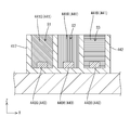
- the LED element 440 in the LED 417 is changed from that in Embodiment 2 described above, and the sealing material 441 that fills each of the divided spaces S1 to S3 of the case 442 is changed.
- the LED element 440 of the LED 417 has a main emission wavelength in the emitted light in a purple wavelength region (about 420 nm to about 480 nm) in visible light, and emits purple light. It can be said that it is a purple LED element emitting monochromatic light.
- the main light emission wavelength of the LED element 440 is preferably about 405 nm, for example.
- a green sealing material 441G containing a green phosphor a red sealing material 441R containing a red phosphor, and main light emission in emitted light.
- a blue sealing material (third sealing material) 441B containing a blue phosphor (third phosphor) having a wavelength in the blue wavelength region is filled.
- the first partitioned space S1 is filled with a green sealing material 441G and contains a green LED element 440G.
- the second section space S2 is filled with a red sealing material 441R and accommodates a red LED element 440R.
- the third section space S3 is filled with the blue sealing material 441B and accommodates the blue LED element 440B.
- the three LED elements 440 are the same as in the second embodiment. Next, the blue phosphor will be described in detail.
- the blue phosphor emits light having a main emission wavelength in a blue wavelength region (about 570 nm to about 600 nm) when excited by light (purple light) from the LED element 440.
- a La oxynitride blue phosphor JEM blue phosphor
- the La oxynitride blue phosphor is an oxynitride represented by the general formula LaAl (Si8-z, Alz) N10-zOz, and is in the (Si, Al)-(O, N) 4 skeleton.
- the structure contains La, and a part of this La is replaced with Ce3 +, whereby a phosphor having Ce3 + as the emission center is obtained.
- the excitation spectrum and emission spectrum of the blue phosphor described above are as shown in FIG.
- the excitation spectrum in the blue phosphor includes a wavelength region ranging from the near-ultraviolet wavelength region to the visible light purple, and the emission spectrum includes the entire blue wavelength region (slightly).
- the main emission wavelength is about 440 nm. Therefore, the blue phosphor does not absorb green light emitted from the green phosphor or red light emitted from the red phosphor.
- the green phosphor can absorb blue light emitted from the blue phosphor as excitation light to some extent (see FIG. 9).
- the red phosphor can absorb the blue light emitted from the blue phosphor together with the green light emitted from the green phosphor to some extent as excitation light (see FIG. 10).
- the LED 417 of the present embodiment configured as described above includes purple light (purple component light) emitted from each LED element 440 (440R, 440G, 440B) and a green phosphor that is the first phosphor. Green light emitted (green component light), red light emitted from the red phosphor as the second phosphor (red component light), and blue light emitted from the blue phosphor as the third phosphor As a whole, it is possible to emit white light as a whole. According to such a configuration, compared with the LED 117 described in the second embodiment, the emission intensity in the violet light, which is the wavelength region on the shorter wavelength side than blue, can be increased, and thus the color rendering property in the emitted light. This is even better.
- the LED element 540 of the LED 517 has a main emission wavelength in the emitted light in the near-ultraviolet wavelength region (about 200 nm to about 380 nm), and emits near-ultraviolet light. It can be said that it is an ultraviolet LED element.
- the main emission wavelength of the LED element 540 is preferably about 380 nm, for example.
- the present invention is not limited to the embodiments described with reference to the above description and drawings.
- the following embodiments are also included in the technical scope of the present invention.
- the LED case in which the LED elements are individually accommodated in each partitioned space is shown.
- the LED elements may be arranged across a plurality of partitioned spaces. Is possible.
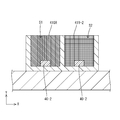
- the LED element 40-1 may be configured to penetrate the partition wall portion 43-1 and to be disposed across the two partition spaces S1 and S2.
- the sealing material filled in each partitioned space in the LED case has been configured to individually contain one type of phosphor.
- the plurality of sealing materials may include a mixture of a plurality of types of phosphors.
- the sealing material 41Y-2 filled in the second section space S2 contains only one kind of yellow phosphor, whereas the seal filled in the first section space S1.
- the stop material 41GR can be configured to contain a green phosphor and a red phosphor.
- the LED elements 40-2 accommodated in the partitioned spaces S1 and S2 emit blue monochromatic light
- the emitted light from the first partitioned space S1 and the emitted light from the second partitioned space S2 are Both are white light. This makes it difficult for color unevenness to occur.
- the case 42-3 constituting the LED 17-3 is divided into two partitioned spaces S1, S2, and the first partitioned space.
- the blue sealing material 41B-3 containing the blue phosphor may be filled in S1
- the yellow sealing material 41Y-3 containing the yellow phosphor may be filled in the second partitioned space S2. Even in such a configuration, the light emitted from the LED 17-3 can be white light with excellent color rendering.
- each sealing material 41-4 is preferably cured at a stage before being accommodated in the case 42-4, so that the different sealing materials 41-4 in the case 42-4. Are difficult to mix.
- the color filters of the color filter included in the liquid crystal panel are exemplified by three colors of R, G, and B.
- the color parts can be four or more colors.
- Y yellow
- R, G, and B which are the three primary colors of light
- a cyan colored portion or the like can be used instead of the yellow colored portion Y.
- the partition wall portion that partitions the internal space of the LED case has the same height as the side wall portion, that is, the height that reaches the opening portion.
- the present invention also includes a relatively low height compared to the portion and a height that does not reach the opening. Conversely, the present invention also includes a configuration in which the partition wall portion is relatively higher than the side wall portion and protrudes outward from the opening portion.
- the partition wall portion that divides the internal space of the LED case is formed integrally with the case.
- the partition wall portion may be a separate part from the case. Included in the invention.
- the internal space of the LED case is divided at approximately equal intervals, but may be divided at unequal pitches.
- the LED elements accommodated in the plurality of partitioned spaces in the LED case are all the same. However, different types (not the same) of LED elements are accommodated. It doesn't matter.
- thermosetting resin material used as the sealing material
- thermoplastic resin material may be used as the sealing material.
- ⁇ -SiAlON is exemplified as the green phosphor used in the LED, but other than that, the green phosphor can be appropriately changed.
- a YAG-based phosphor as the green phosphor because highly efficient light emission can be obtained.
- a YAG-based phosphor has a garnet structure composed of a complex oxide of yttrium and aluminum, and is represented by the chemical formula: Y3Al5O12, and a rare earth element (for example, Ce, Tb, Eu, Nd, etc.) as an activator. Is used.
- Specific YAG phosphors include, for example, Y3Al5O12: Ce, Y3Al5O12: Tb, (Y, Gd) 3Al5O12: Ce, Y3 (Al, Ga) 5O12: Ce, Y3 (Al, Ga) 5O12: Tb, (Y, Gd) 3 (Al, Ga) 5O12: Ce, (Y, Gd) 3 (Al, Ga) 5O12: Tb, Tb3Al5O12: Ce, and the like.
- casoon is exemplified as the red phosphor used in the LED, but the red phosphor can be appropriately changed.
- ⁇ -SiAlON is exemplified as the yellow phosphor used in the LED, but other than that, the yellow phosphor can be appropriately changed.
- BOSE BOSE uses Eu (europium) as an activator, and is represented by (Ba ⁇ Sr) 2 SiO 4: Eu.
- the yellow phosphor can be changed.
- (Y, Gd) 3Al3O12: Ce which is a YAG-based phosphor, is used, highly efficient light emission can be obtained.
- Tb3Al5O12: Ce or the like can be used as the yellow phosphor.
- the TFT is used as the switching element of the liquid crystal display device.
- the present invention can also be applied to a liquid crystal display device using a switching element other than TFT (for example, a thin film diode (TFD)).
- a switching element other than TFT for example, a thin film diode (TFD)
- the present invention can be applied to a liquid crystal display device for monochrome display.
- the liquid crystal display device using the liquid crystal panel as the display panel has been exemplified.
- the present invention can also be applied to display devices using other types of display panels.
- the television receiver provided with the tuner substrate is illustrated, but the present invention can also be applied to a display device that does not include the tuner substrate.
- the LED used in the backlight device constituting the liquid crystal display device has been exemplified.
- an LED that is a light source used for general lighting applications for example, an alternative to an incandescent bulb
- the present invention is also applicable.
- SYMBOLS 10,310 Liquid crystal display device (display device) 11, 311 ... Liquid crystal panel (display panel), 12, 312 ... Backlight device (illumination device) 14, 314 ... Chassis (housing), 14c, 314c ... Opening Part, 15,315 ... optical member, 17, 117, 217, 317, 417, 517 ... LED (light source), 40, 140, 240, 440, 540 ... LED element (light emitting element), 41, 141, 241, 441 , 541 ... Sealing material (translucent resin material), 42, 142, 242, 442, 542 ... Case (container), 42c ... Opening, 43, 143 ... Partition wall, S1 ... First partition space ( Section space), S2 ... Second section space (section space), S3 ... Third section space (section space)
Landscapes
- Physics & Mathematics (AREA)
- Nonlinear Science (AREA)
- Mathematical Physics (AREA)
- Chemical & Material Sciences (AREA)
- Crystallography & Structural Chemistry (AREA)
- General Physics & Mathematics (AREA)
- Optics & Photonics (AREA)
- Led Device Packages (AREA)
- Planar Illumination Modules (AREA)
Abstract
本発明に係る光源は、LED(光源)17は、LED素子(発光素子)40と、LED素子40からの光により励起されて光を発するものであって、その発光光における主発光波長が互いに異なる複数種類の蛍光体と、LED素子40が収容されるとともに、内部空間において複数種類の蛍光体がそれぞれ偏在して配されるケース(収容体)42とを備える。蛍光体としては、緑色蛍光体と赤色蛍光体との2種類が用いられ、これらがケース42内において区分壁部43によって区分された各区分空間S1,S2に種類毎に配されている。
Description
本発明は、光源、照明装置及び表示装置に関する。
近年、白熱電球の代替光源や、液晶表示装置の外部光源として、低消費電力で且つ長寿命なLEDが用いられるケースが増えている。LEDは、LED基板上に実装されており、発光源であるLEDチップと、LEDチップからの光により励起されて所定の色の光を発する蛍光体を含有した封止材と、LEDチップを収容するとともに封止材が充填されるハウジングとからなる。なお、上記のようなLEDの一例として下記特許文献1に記載されたものが知られている。
(発明が解決しようとする課題)
ところで、白色光を発するLEDには様々な構成を採ることが考えられるが、例えばLEDチップとして青色光を発するものを用いるとともに、封止材に緑色光を発する緑色蛍光体と赤色光を発する赤色蛍光体とを混合させたものを用いる構成とすれば、仮に青色光を発するLEDチップに、蛍光体として黄色光を発する黄色蛍光体のみを単一で用いた場合よりも、演色性において優れるというメリットを享受できる。ところが、封止材に2種類の蛍光体を混在させると、発光効率が悪化するおそれがあり、その点において未だ改善の余地があった。
ところで、白色光を発するLEDには様々な構成を採ることが考えられるが、例えばLEDチップとして青色光を発するものを用いるとともに、封止材に緑色光を発する緑色蛍光体と赤色光を発する赤色蛍光体とを混合させたものを用いる構成とすれば、仮に青色光を発するLEDチップに、蛍光体として黄色光を発する黄色蛍光体のみを単一で用いた場合よりも、演色性において優れるというメリットを享受できる。ところが、封止材に2種類の蛍光体を混在させると、発光効率が悪化するおそれがあり、その点において未だ改善の余地があった。
本発明は上記のような事情に基づいて完成されたものであって、発光効率を向上させることを目的とする。
(課題を解決するための手段)
本発明の光源は、発光素子と、前記発光素子からの光により励起されて光を発するものであって、その発光光における主発光波長が互いに異なる複数種類の蛍光体と、前記発光素子が収容されるとともに、内部空間において複数種類の前記蛍光体がそれぞれ偏在して配される収容体とを備える。
本発明の光源は、発光素子と、前記発光素子からの光により励起されて光を発するものであって、その発光光における主発光波長が互いに異なる複数種類の蛍光体と、前記発光素子が収容されるとともに、内部空間において複数種類の前記蛍光体がそれぞれ偏在して配される収容体とを備える。
このようにすれば、発光素子からの光により励起されて光を発する蛍光体として主発光波長が互いに異なる複数種類のものを用いているから、当該光源の出射光に係る演色性を優れたものとすることができる。その上で、収容体の内部空間には、複数種類の蛍光体がそれぞれ偏在して配されているから、仮に複数種類の蛍光体をランダムに混在させた場合に比べると、発光素子からの光により励起されて各蛍光体から発せられる光が、発光元とは別の種類の蛍光体によって吸収され難くなる。これにより、複数種類の蛍光体から発せられる光をそれぞれ低損失でもって当該光源の出射光として有効に利用することができ、もって発光効率を高めることができる。
本発明の実施態様として、次の構成が好ましい。
(1)前記収容体の内部空間を、複数種類の前記蛍光体がそれぞれ対応付けられて存する複数の区分空間に区分する区分壁部が備えられている。このようにすれば、収容体の内部空間が区分壁部によって複数の区分空間に区分されることで、各区分空間に対応付けられて存する各蛍光体から発せられた光が、発光元の蛍光体が存する区分空間とは別の区分空間に入るのが防がれるとともに、その別の区分空間に存する発光元とは別の種類の蛍光体によって吸収されるのが防がれる。これにより、各蛍光体から発せられる光を一層低損失で利用することができ、発光効率を一層高いものとすることができる。
(1)前記収容体の内部空間を、複数種類の前記蛍光体がそれぞれ対応付けられて存する複数の区分空間に区分する区分壁部が備えられている。このようにすれば、収容体の内部空間が区分壁部によって複数の区分空間に区分されることで、各区分空間に対応付けられて存する各蛍光体から発せられた光が、発光元の蛍光体が存する区分空間とは別の区分空間に入るのが防がれるとともに、その別の区分空間に存する発光元とは別の種類の蛍光体によって吸収されるのが防がれる。これにより、各蛍光体から発せられる光を一層低損失で利用することができ、発光効率を一層高いものとすることができる。
(2)複数種類の前記蛍光体は、複数の前記区分空間のそれぞれに各種類毎に個別に存するものとされる。このようにすれば、各区分空間と蛍光体の種類とが一対一で対応付けられているから、各区分空間に存する各蛍光体から発せられた光が、それぞれ発光元とは別の種類の蛍光体によって吸収されるのを確実に防ぐことができる。これにより、各蛍光体から発せられる光をより一層低損失で利用することができ、発光効率をより一層高いものとすることができる。
(3)前記発光素子は、複数の前記区分空間のそれぞれに個別に配されている。このようにすれば、各区分空間に対応して各発光素子の出力を個別に制御することが可能となる。これにより、当該光源の出射光における色味や輝度の調整などを行う上で有用である。
(4)複数の前記区分空間のそれぞれに個別に配される前記発光素子には、同一のものが用いられている。このようにすれば、発光素子の調達コストを低く抑えることができる。また、各発光素子における入出力特性が統一されるから、各発光素子の出力を制御するための回路構成などを簡素化することができる。
(5)前記区分壁部は、前記収容体に一体形成されている。このようにすれば、仮に区分壁部を収容体とは別部品とした場合に比べると、製造時の組付工数などを削減することができて製造コストの低減に好適となる。
(6)前記収容体には、前記発光素子及び前記蛍光体からの光を出射させる開口部が形成されており、前記区分壁部は、前記開口部に至る高さを有している。このようにすれば、区分壁部が開口部に至る高さを有しているから、各蛍光体からの光が開口部から出射されるまでの間に、発光元とは別の種類の蛍光体によって吸収されるのをより確実に防ぐことができる。
(7)前記区分壁部は、前記収容体の内部空間をほぼ等間隔に区分するよう配されている。このようにすれば、各蛍光体が配される各区分空間の容積をほぼ等しくすることができる。
(8)前記蛍光体を含有する透光性樹脂材料が複数備えられており、複数の前記透光性樹脂材料は、前記収容体の内部空間において互いに異なる領域にそれぞれ偏在するよう充填されている。このようにすれば、収容体内に充填される透光性樹脂材料に蛍光体を含有させるようにしているから、複数種類の蛍光体を収容体内において容易に偏在させることができる。
(9)複数の前記透光性樹脂材料は、複数種類の前記蛍光体を各種類毎に個別に含有している。このようにすれば、各透光性樹脂材料と蛍光体の種類とが一対一で対応付けられているから、仮に複数の透光性樹脂材料のうちの1つに、複数種類の蛍光体を混在させた透光性樹脂材料を含ませた場合に比べると、各蛍光体から発せられた光が、それぞれ発光元とは別の種類の蛍光体によってより吸収され難くなる。これにより、各蛍光体から発せられる光をより低損失でもって出射光として利用することができ、発光効率をより高いものとすることができる。
(10)前記発光素子は、発光光における主発光波長が青色の波長領域に存する青色発光素子とされるのに対し、複数種類の前記蛍光体には、発光光における主発光波長が緑色の波長領域に存する緑色蛍光体と、発光光における主発光波長が赤色の波長領域に存する赤色蛍光体とが含まれている。このようにすれば、青色発光素子からの青色光と、緑色蛍光体からの緑色光と、赤色蛍光体からの赤色光とによって、全体として演色性に優れた略白色光を出射することができる。
(11)複数種類の前記蛍光体には、発光光における主発光波長が黄色の波長領域に存する黄色蛍光体が含まれている。このようにすれば、蛍光体として緑色蛍光体及び赤色蛍光体に、さらに黄色蛍光体を加えることで、さらに演色性を向上させることができる。
(12)前記発光素子は、LED素子とされる。このようにすれば、低消費電力になるとともに長寿命となる。
次に、上記課題を解決するために、本発明の照明装置は、上記記載の光源と、前記光源を収容するとともに光出射側に開口部を有する筐体と、前記開口部を覆うようにして配されるとともに前記光源からの光を透過する光学部材とを備える。このような照明装置によると、光源が演色性及び発光効率に優れたものであるから、演色性の向上を図ることができるとともに輝度の向上または低消費電力化を図ることができる。
さらには、上記課題を解決するために、本発明の表示装置は、上記記載の照明装置と、前記照明装置からの光を利用して表示を行う表示パネルとを備える。このような表示装置によると、表示パネルに対して光を供給する照明装置が、演色性の向上を図られるとともに輝度の向上または低消費電力化を図られたものであるから、表示品質の優れた表示を実現することができるとともに、輝度の向上または低消費電力化を図ることができる。
前記表示パネルとしては液晶パネルを例示することができる。このような表示装置は液晶表示装置として、種々の用途、例えばテレビやパソコンのディスプレイ等に適用でき、特に大型画面用として好適である。
(発明の効果)
本発明によれば、発光効率を向上させることができる。
本発明によれば、発光効率を向上させることができる。
<実施形態1>
本発明の実施形態1を図1から図17によって説明する。本実施形態では、液晶表示装置10について例示する。なお、各図面の一部にはX軸、Y軸及びZ軸を示しており、各軸方向が各図面で示した方向となるように描かれている。また、図3及び図4に示す上側を表側とし、同図下側を裏側とする。
本発明の実施形態1を図1から図17によって説明する。本実施形態では、液晶表示装置10について例示する。なお、各図面の一部にはX軸、Y軸及びZ軸を示しており、各軸方向が各図面で示した方向となるように描かれている。また、図3及び図4に示す上側を表側とし、同図下側を裏側とする。
本実施形態に係るテレビ受信装置TVは、図1に示すように、液晶表示装置10と、当該液晶表示装置10を挟むようにして収容する表裏両キャビネットCa,Cbと、電源Pと、チューナーTと、スタンドSとを備えて構成される。液晶表示装置(表示装置)10は、全体として横長(長手)の方形状(矩形状)をなし、縦置き状態で収容されている。この液晶表示装置10は、図2に示すように、表示パネルである液晶パネル11と、外部光源であるバックライト装置(照明装置)12とを備え、これらが枠状のベゼル13などにより一体的に保持されるようになっている。
先に、液晶パネル11について説明する。液晶パネル11は、図5に示すように、一対の透明な(透光性を有する)ガラス製の基板20,21間に、電界印加に伴って光学特性が変化する物質である液晶材料を含む液晶層22を封入してなる。液晶パネル11を構成する両基板20,21のうち裏側(バックライト装置12側)に配されるものが、アレイ基板(基板、アクティブマトリクス基板)20とされ、表側(光出射側)に配されるものが、CF基板(対向基板)21とされている。なお、両基板20,21の外面側には、表裏一対の偏光板23がそれぞれ貼り付けられている。
アレイ基板20における内面側(液晶層22側、CF基板21との対向面側)には、図6に示すように、3つの電極24a~24cを有するスイッチング素子であるTFT(Thin Film Transistor)24及び画素電極25が多数個並んで設けられるとともに、これらTFT24及び画素電極25の周りには、格子状をなすゲート配線26及びソース配線27が取り囲むようにして配設されている。画素電極25は、ITO(Indium Tin Oxide)などの透明導電膜からなる。ゲート配線26及びソース配線27は、共に導電材料からなる。ゲート配線26とソース配線27とがそれぞれTFT24のゲート電極24aとソース電極24bとに接続され、画素電極25がドレイン配線(図示せず)を介してTFT24のドレイン電極24cに接続されている。アレイ基板20には、ゲート配線26に並行するとともに画素電極25に対して平面に視て重畳する容量配線(補助容量配線、蓄積容量配線、Cs配線)33が設けられている。容量配線33は、Y軸方向についてゲート配線26と交互に配されている。ゲート配線26がY軸方向に隣り合う画素電極25の間に配されているのに対し、容量配線33は、各画素電極25におけるY軸方向のほぼ中央部を横切る位置に配されている。このアレイ基板20の端部には、ゲート配線26及び容量配線33から引き回された端子部及びソース配線27から引き回された端子部が設けられており、これらの各端子部には、図示しない外部回路から各信号または基準電位が入力されるようになっており、それによりTFT24の駆動が制御される。また、アレイ基板20の内面側には、液晶層22に含まれる液晶分子を配向させるための配向膜28が形成されている(図5)。
一方、CF基板21における内面側(液晶層22側、アレイ基板20との対向面側)には、図5及び図7に示すように、アレイ基板20側の各画素電極25と平面に視て重畳する位置に多数個のカラーフィルタが並んで設けられている。カラーフィルタは、R(赤色),G(緑色),B(青色)を呈する各着色部29がX軸方向に沿って交互に並ぶ配置とされる。また、各着色部29の外形は、画素電極25の外形に倣って平面に視て縦長の方形状をなしている。カラーフィルタを構成する各着色部29間には、混色を防ぐための格子状をなす遮光部(ブラックマトリクス)30が形成されている。遮光部30は、アレイ基板20側のゲート配線26、ソース配線27及び容量配線33に対して平面視重畳する配置とされる。また、各着色部29及び遮光部30の表面には、アレイ基板20側の画素電極25と対向する対向電極31が設けられている。また、CF基板21の内面側には、液晶層22に含まれる液晶分子を配向させるための配向膜32がそれぞれ形成されている。
続いて、バックライト装置12について詳しく説明する。バックライト装置12は、図2に示すように、表側、つまり光出射側(液晶パネル11側)に開口する開口部14cを有した略箱型をなすシャーシ14と、シャーシ14の開口部14cを覆う形で配される光学部材15と、次述する導光部材19を表側から押さえるフレーム16とを備えている。さらにはシャーシ14内には、光源であるLED(Light Emitting Diode:発光ダイオード)17が実装されたLED基板(光源基板)18と、LED17からの光を導光して光学部材15(液晶パネル11、光出射側)へと導く導光部材19とが収容されている。そして、このバックライト装置12は、その長辺側の両端部に、LED17を有するLED基板18をそれぞれ備えるとともに、両端側に配されたLED基板18間に挟まれた中央側に導光部材19を配置してなる、いわゆるエッジライト型(サイドライト型)とされている。以下では、バックライト装置12の各構成部品について詳しく説明する。
シャーシ14は、例えばアルミニウム板や電気亜鉛めっき綱板(SECC)などの金属板からなり、図2から図4に示すように、液晶パネル11と同様に横長の方形状をなす底板14aと、底板14aにおける各辺(一対の長辺及び一対の短辺)の外端からそれぞれ表側に向けて立ち上がる側板14bとからなる。シャーシ14(底板14a)は、その長辺方向がX軸方向(水平方向)と一致し、短辺方向がY軸方向(鉛直方向)と一致している。また、側板14bには、フレーム16及びベゼル13がねじ止め可能とされる。
光学部材15は、図2に示すように、液晶パネル11及びシャーシ14と同様に平面に視て横長の方形状をなしている。光学部材15は、導光部材19の表側(光出射側)に載せられていて液晶パネル11と導光部材19との間に介在して配されることで、導光部材19からの出射光を透過するとともにその透過光に所定の光学作用を付与しつつ液晶パネル11に向けて出射させる。光学部材15は、裏側(導光部材19側、光出射側とは反対側)に配される拡散板15aと、表側(液晶パネル11側、光出射側)に配される光学シート15bとから構成される。拡散板15aは、所定の厚みを持つほぼ透明な合成樹脂製の基材内に拡散粒子を多数分散して設けた構成とされ、透過する光を拡散させる機能を有する。光学シート15bは、拡散板15aに比べると板厚が薄いシート状をなしており、3枚が積層して配されている(図2)。具体的な光学シート15bの種類としては、例えば拡散シート、レンズシート、反射型偏光シートなどがあり、これらの中から適宜に選択して使用することが可能である。なお、図3及び図4では、都合上3枚の光学シート15bを1枚に簡略化して図示している。
フレーム16は、図2に示すように、導光部材19の外周端部に沿って延在する枠状(額縁状)に形成されており、導光部材19の外周端部をほぼ全周にわたって表側から押さえることが可能とされる。このフレーム16は、合成樹脂製とされるとともに、表面が例えば黒色を呈する形態とされることで、遮光性を有するものとされる。フレーム16のうち両長辺部分における裏側の面、つまり導光部材19及びLED基板18(LED17)との対向面には、図3に示すように、光を反射させる第1反射シートR1がそれぞれ取り付けられている。第1反射シートR1は、フレーム16の長辺部分におけるほぼ全長にわたって延在する大きさを有しており、導光部材19におけるLED17と対向状をなす端部に直接当接されるとともに導光部材19の上記端部とLED基板18とを一括して表側から覆うものとされる。また、フレーム16は、液晶パネル11における外周端部を裏側から受けることができる。
LED17は、図2及び図3に示すように、LED基板18上に表面実装されるとともにその発光面17aがLED基板18側とは反対側を向いた、いわゆるトップ型とされている。なお、LED17の詳しい構成に関しては後に詳しく説明する。LED基板18は、表面が光の反射性に優れた白色を呈する合成樹脂製(ガラスエポキシ樹脂など)とされ、図2に示すように、シャーシ14の長辺方向(導光部材19におけるLED17側の端部、X軸方向)に沿って延在する、長手の板状をなしており、その板面をX軸方向及びZ軸方向に並行させた姿勢、すなわち液晶パネル11及び導光部材19(透光性光学部材15)の板面と直交させた姿勢でシャーシ14内に収容されている。つまり、このLED基板18は、板面における長辺方向がX軸方向と、短辺方向がZ軸方向とそれぞれ一致し、さらには板面と直交する板厚方向がY軸方向と一致した姿勢とされる。
LED基板18は、図2及び図3に示すように、Y軸方向について導光部材19を挟んだ位置に対をなして配されており、詳しくは導光部材19とシャーシ14における長辺側の各側板14bとの間に介在するようそれぞれ配され、シャーシ14に対してはZ軸方向に沿って表側から収容されるようになっている。LED基板18の板面のうち、内側、つまり導光部材19側を向いた面(導光部材19との対向面)には、複数(図5では27個)のLED17がLED基板18の長辺方向(透光性光学部材15の長辺方向、X軸方向)に沿って間欠的に並列して配されており、この一列に並列したLED17によりLED群が構成されている。各LED17は、LED基板18における導光部材19側を向いた面に表面実装されており、ここが実装面とされている。LED基板18の実装面には、X軸方向に沿って延在するとともにLED群を横切って隣り合うLED17同士を直列接続する、金属膜(銅箔など)からなる配線パターン(図示せず)が形成されており、この配線パターンの両端部に形成された端子部が外部の駆動回路に接続されることで、駆動電力を各LED17に供給することが可能とされる。このLED基板18は、板面の片面のみが実装面とされる片面実装タイプとされている。X軸方向について隣り合うLED17間の間隔、つまりLED17の配列ピッチは、ほぼ等しいものとされる。各LED基板18は、実装面とは反対側の板面がシャーシ14における長辺側の各側板14bの内面に接する形でそれぞれ取り付けられている。従って、各LED基板18にそれぞれ実装された各LED17の発光面17aが対向状をなすとともに、各LED17における光軸がY軸方向とほぼ一致する。なお、LED基板18に用いる素材としては、例えばシャーシ14と同じアルミ系材料などの金属材料とし、その表面に絶縁層を介して配線パターンを形成された構成とすることも可能である。
導光部材19は、屈折率が空気よりも十分に高く且つほぼ透明な(透光性に優れた)合成樹脂材料(例えばアクリルなど)からなる。導光部材19は、図2に示すように、液晶パネル11及びシャーシ14と同様に平面に視て横長の方形状をなす板状とされており、その板面における長辺方向がX軸方向と、短辺方向がY軸方向とそれぞれ一致し、且つ板面と直交する板厚方向がZ軸方向と一致している。導光部材19は、図3に示すように、シャーシ14内において液晶パネル11及び光学部材15の直下位置に配されており、シャーシ14における長辺側の両端部に配された対をなすLED基板18間にY軸方向について挟み込まれる形で配されている。従って、LED17(LED基板18)と導光部材19との並び方向がY軸方向と一致するのに対して、光学部材15(液晶パネル11)と導光部材19との並び方向がZ軸方向と一致しており、両並び方向が互いに直交するものとされる。そして、導光部材19は、LED17からY軸方向に向けて発せられた光を導入するとともに、その光を内部で伝播させつつ光学部材15側(表側、光出射側)へ向くよう立ち上げて出射させる機能を有する。この導光部材19は、シャーシ14の底板14aにおいてその短辺方向の中央位置に配されていることから、底板14aにおける短辺方向の中央部分により裏側から支持されていると言える。なお、導光部材19は、上記した光学部材15よりも一回り大きく形成されており、その外周端部が光学部材15の外周端面よりも外側に張り出すとともに既述したフレーム16により押さえられるものとされる(図3)。
導光部材19は、図3及び図4に示すように、シャーシ14の底板14a及び光学部材15の各板面に沿って延在する略平板状をなしており、その板面がX軸方向及びY軸方向に並行するものとされる。導光部材19の板面のうち、表側を向いた面が内部の光を光学部材15及び液晶パネル11に向けて出射させる光出射面19aとなっている。導光部材19における板面に対して隣り合う外周端面のうち、X軸方向に沿って長手状をなす長辺側の両端面は、図3に示すように、それぞれLED17(LED基板18)と所定の空間を空けて対向状をなしており、これらがLED17から発せられた光が入射される光入射面19bとなっている。このLED17と光入射面19bとの間に保有される空間の表側には、既述した第1反射シートR1が配されているのに対し、同空間の裏側には、第1反射シートR1との間で同空間を挟み込む形で第2反射シートR2が配されている。両反射シートR1,R2は、上記空間に加えて導光部材19におけるLED17側の端部及びLED17をも挟み込む形で配されている。これにより、LED17からの光を両反射シートR1,R2間で繰り返し反射することで、光入射面19bに対して効率的に入射させることができる。また、光入射面19bは、X軸方向及びZ軸方向に沿って並行する面とされ、光出射面19aに対して略直交する面とされる。また、LED17と光入射面19bとの並び方向は、Y軸方向と一致しており、光出射面19aに並行している。
導光部材19の板面のうち、光出射面19aとは反対側の面19cには、図3及び図4に示すように、導光部材19内の光を反射して表側へ立ち上げることが可能な第3反射シートR3がその全域を覆う形で設けられている。言い換えると、第3反射シートR3は、シャーシ14の底板14aと導光部材19との間に挟まれた形で配されている。なお、導光部材19における光出射面19aと反対側の面19cとの少なくともいずれか一方、または第3反射シートR3の表面には、導光部材19内の光を散乱させる散乱部(図示せず)などが所定の面内分布を持つようパターニングされており、それにより光出射面19aからの出射光が面内において均一な分布となるよう制御されている。
ここで、LED17の構成について詳しく説明する。LED17は、図8に示すように、発光源であるLED素子(LEDチップ、発光素子)40と、LED素子40からの光によって励起されることで発光する蛍光体を含有する封止材(透光性樹脂材料)41と、LED素子40が収容されるとともに封止材41が充填されるケース(収容体)42とを備える。このLED17は、発光面17aから発せられる出射光が全体として略白色光とされている。以下、図8を参照しつつLED17の構成部品について順次に詳しく説明する。
LED素子40は、例えばInGaN系の材料からなる半導体であり、順方向に電圧が印加されることで発光するものとされる。LED素子40は、その発光光における主発光波長が青色の波長領域(約420nm~約480nm)に存しており、青色光を単色発光する青色LED素子であると言える。LED素子40の主発光波長は、440nm~460nmの範囲とされるのがより好ましく、具体的には例えば451nmとされる。LED素子40は、図示しないリードフレームによってケース42外に配されたLED基板18における配線パターンに接続される。
封止材41は、ほぼ透明な熱硬化性樹脂材料からなるものとされ、具体的にはエポキシ樹脂材料やシリコーン樹脂材料などからなる。封止材41は、LED17の製造工程ではLED素子40が収容されたケース42の内部空間に充填されることで、LED素子40及びリードフレームを封止するとともにこれらの保護を図るものとされる。この封止材41には、次述する蛍光体が分散配合されており、蛍光体を保持する分散媒(バインダ)として機能する。
蛍光体は、LED素子40からの光(青色光)によって励起されることで、所定の波長領域に存する光を発光するものであり、本実施形態に係るLED17においては蛍光体として発光光(蛍光)における主発光波長が互いに異なる2種類のもの(次述する第1の蛍光体及び第2の蛍光体)が用いられている。具体的には、第1の蛍光体は、LED素子40からの光に励起されることで、主発光波長が緑色の波長領域(約500nm~約570nm)に存する光を発する緑色蛍光体とされる。第2の蛍光体は、LED素子40からの光に励起されることで、主発光波長が赤色の波長領域(約600nm~約780nm)に存する光を発する赤色蛍光体とされる。
従って、このLED17は、LED素子40から発せられる青色光(青色成分の光)と、第1の蛍光体である緑色蛍光体から発せられる緑色光(緑色成分の光)と、第2の蛍光体である赤色蛍光体から発せられる赤色光(赤色成分の光)とにより、全体として概ね白色の光を発することが可能とされている。このような構成によれば、仮に蛍光体として、緑色蛍光体及び赤色蛍光体に代えて黄色光を発する黄色蛍光体を用いることで、白色光を発する構成とした場合に比べると、緑色光及び赤色光における発光強度を高くすることができ、もって出射光における演色性の点で優れる。このLED17における出射光の色度は、例えば緑色蛍光体及び赤色蛍光体における含有量の絶対値や相対値に応じて変化するものとされるため、これら緑色蛍光体及び赤色蛍光体の含有量を適宜調整することでLED17における出射光の色度を調整することが可能とされる。
上記した緑色蛍光体としては、サイアロン系蛍光体の一種であるβ-SiAlONを用いるのが好ましい。サイアロン系蛍光体は、窒化ケイ素のシリコン原子の一部がアルミニウム原子に、窒素原子の一部が酸素原子に置換された物質、つまり窒化物である。窒化物であるサイアロン系蛍光体は、例えば硫化物や酸化物などからなる他の蛍光体に比べると、発光効率に優れるとともに耐久性に優れている。ここで言う「耐久性に優れる」とは、具体的には、LED素子40からの高いエネルギーの励起光に曝されても経時的に輝度低下が生じ難いことなどを意味する。サイアロン系蛍光体には、付活剤として希土類元素(例えばTb,Yg,Agなど)が用いられる。サイアロン系蛍光体の一種であるβ-SiAlONは、β型窒化ケイ素結晶にアルミニウムと酸素とが固溶した一般式Si6-zAlzOzN8-z:Eu(zは固溶量を示す)または(Si,Al)6(O,N)8:Euにより表される物質である。本実施形態に係るβ-SiAlONには、付活剤として例えばEu(ユーロピウム)が用いられており、それにより発光光である緑色光の色純度が特に高いものとされる。なお、本実施形態に係る緑色蛍光体であるβ-SiAlONは、その発光光の主発光波長が例えば約540nm程度とされる(図9参照)。
一方、赤色蛍光体としては、カズン系蛍光体の一種であるカズンを用いるのが好ましい。カズン系蛍光体は、カルシウム原子(Ca)、アルミニウム原子(Al)、ケイ素原子(Si)、窒素原子(N)を含む窒化物であり、例えば硫化物や酸化物などからなる他の蛍光体に比べると、発光効率に優れるとともに耐久性に優れている。カズン系蛍光体は、付活剤として希土類元素(例えばTb,Yg,Agなど)が用いられる。カズン系蛍光体の一種であるカズンは、付活剤としてEu(ユーロピウム)が用いられるとともに、組成式CaAlSiN3:Euにより示される。なお、本実施形態に係る赤色蛍光体であるカズンは、その発光光の主発光波長が例えば約650nm程度とされる(図10参照)。
ケース42は、表面が光の反射性に優れた白色を呈する合成樹脂材料(例えばポリアミド系樹脂材料)またはセラミック材料からなる。ケース42は、全体として光出射側(発光面17a側、LED基板18側とは反対側)に開口部42cを有する略箱型をなしており、大まかにはLED基板18の実装面に沿って延在する底壁部42aと、底壁部42aの外縁から立ち上がる側壁部42bとを有している。このうち底壁部42aは、光出射側から視て方形状をなしているのに対し、側壁部42bは、底壁部42aの外周縁に沿う略角筒状をなしていて光出射側から視ると方形の枠状をなしている。ケース42を構成する底壁部42aの内面(底面)には、LED素子40が配置されている。これに対して側壁部42bには、リードフレームが貫通されている。リードフレームのうち、ケース42内に配される端部がLED素子40に接続されるのに対し、ケース42外に導出される端部がLED基板18の配線パターンに接続される。
ここで、LED17に含まれる2種類の蛍光体における励起スペクトル及び発光スペクトルについて説明する。緑色蛍光体(第1の蛍光体)における励起スペクトル及び発光スペクトルは図9に示す通りであり、赤色蛍光体(第2の蛍光体)における励起スペクトル及び発光スペクトルは図10に示す通りである。先に前者について説明すると、緑色蛍光体における励起スペクトルは、図9に示すように、近紫外線の波長領域、可視光線における紫色、青色、緑色の一部(短波長側の一部)にわたる波長領域を含んでおり、発光スペクトルは、緑色の波長領域の全域を含んでいて(僅かに青色、黄色の波長領域をも含む)、その主発光波長が約540nm程度とされる。後者について説明すると、赤色蛍光体における励起スペクトルは、図10に示すように、近紫外線の波長領域、可視光線の紫色、青色、緑色、黄色の一部(短波長側の一部)にわたる波長領域を含んでおり、発光スペクトルは、赤色の波長領域の全域を含んでいて(僅かに緑色、黄色の波長領域をも含む)、その主発光波長が約650nm程度とされる。つまり、緑色蛍光体は、赤色蛍光体から発せられる赤色光を励起光として吸収することは殆どないものの、赤色蛍光体は、緑色蛍光体から発せられる緑色光を励起光としてある程度吸収する性質を有していると言える。このことは、図10において赤色蛍光体の励起スペクトルに緑色蛍光体の主発光波長である540nmが含まれていることから明らかである。このため、従来のように同一の封止材に緑色蛍光体及び赤色蛍光体を混合し、封止材中に緑色蛍光体及び赤色蛍光体がランダムに混在する構成とした場合には、緑色蛍光体から発せられる緑色光が赤色蛍光体によって吸収されてそこで損失が生じるために全体の発光効率が悪化する、という問題が生じるおそれがあった。
そこで、本実施形態に係るLED17においては、発光光における主発光波長が互い異なる2種類の蛍光体が、LED17内においてそれぞれ偏在して配される構成を採用している。すなわち、上記2種類の蛍光体には、それぞれ種類毎に専用の封止材41が用意されており、それら専用の封止材41に対して各蛍光体が1種類ずつ(一対一で対応付けられて)、それぞれ分散配合されているので、封止材41において異なる種類の蛍光体同士が混ざることがないものとされる。そして、互いに異なる蛍光体を含有した2種類の封止材41が、ケース42の内部空間において互いに異なる領域に偏在するよう充填されているのである。これにより、従来のように2種類の蛍光体をランダムに混在させた場合に比べると、緑色蛍光体から発せられた緑色光が赤色蛍光体によって吸収され難くなり、もってLED17の発光効率を向上させることができる。封止材41には、2種類の蛍光体のうちの緑色蛍光体(第1の蛍光体)のみを含有する緑色用封止材(第1の封止材)41Gと、赤色蛍光体(第2の蛍光体)のみを含有する赤色用封止材(第2の封止材)41Rとの2種類が存在していることになる。なお、封止材41を区別する場合には、緑色蛍光体のみを含有する緑色用封止材の符号に添え字Gを、赤色蛍光体のみを含有する赤色用封止材の符号に添え字Rを付し、区別せずに総称する場合には、符号に添え字を付さないものとする。
そして、上記したようにケース42内において2種類の封止材41G,41Rをそれぞれ偏在させるべく、ケース42には、その内部空間を2つの区分空間S1,S2に区分する区分壁部43が設けられている。区分壁部43は、ケース42に一体形成されており、底壁部42aから側壁部42bに沿って立ち上がる形態とされている。これにより、各区分空間S1,S2に充填された2種類の封止材41G,41Rに含まれる各蛍光体から発せられた光のうち、隣り合う区分空間S1,S2へ向かうものは、区分壁部43によって反射または吸収されることで隣り合う区分空間S1,S2内に入ることが確実に防止される。もって、緑色蛍光体から発せられた緑色光が赤色蛍光体によって吸収されるのを確実に防ぐことができる。詳しくは、区分壁部43は、底壁部42aのうちX軸方向の中央位置に配されるとともに、Y軸方向及びZ軸方向に沿った板面を有する平板状をなしている。つまり、区分壁部43は、ケース42の内部空間をX軸方向についてほぼ等間隔に区分しており、X軸方向について左右に並ぶ一対の区分空間S1,S2は、容積が互いにほぼ等しいものとされている。また、区分壁部43は、底壁部42aからの立ち上がり高さがケース42の全高とほぼ等しく、その立ち上がり先端部が開口部42cに達している。区分壁部43は、その立ち上がり先端面が側壁部42bの先端面及びLED17の発光面17aと面一状をなしている。
そして、上記した2種類の封止材41G,41Rは、ケース42における2つの区分空間S1,S2にそれぞれ種類毎に個別に(一対一で対応付けられて)充填されている。具体的には、図8に示す左側の第1区分空間S1には、緑色用封止材41Gのみが充填されるのに対し、同図右側の第2区分空間S2には、赤色用封止材41Rのみが充填されている。これにより、ケース42の内部空間には、緑色用封止材41Gと赤色用封止材41RとがX軸方向について左右にそれぞれ偏在して存するものとされる。その上で、ケース42における2つの区分空間S1,S2には、それぞれLED素子40が個別に配されている。つまり、LED素子40には、緑色用封止材(第1の封止材)41Gにより封止されるとともに緑色蛍光体に対してのみ励起光を供給する緑色用LED素子(第1のLED素子)41Gと、赤色用封止材(第2の封止材)41Rにより封止されるとともに赤色蛍光体に対してのみ励起光を供給する赤色用LED素子(第2のLED素子)41Rとの2つが存在していることになる。これら2つのLED素子40G,40Rは、同一のものであり、共に既述した通り青色の単色光を発するものとされる。なお、LED素子40を区別する場合には、緑色用封止材41Gにより封止される緑色用LED素子の符号に添え字Gを、赤色用封止材41Rにより封止される赤色用LED素子の符号に添え字Rを付し、区別せずに総称する場合には、符号に添え字を付さないものとする。
<比較実験>
続いて、本実施形態に係るLED17の優位性を実証すべく、下記の比較実験を行った。この比較実験では、2種類の蛍光体を1つの封止材に混合したLED17COを用いた比較例と、本実施形態に係るLED17を用いた実施例とで、各LED17,17COの出射光における各色(青色(B)、緑色(G)、赤色(R))の光の発光強度をそれぞれ測定した。比較例に係るLED17COは、図11に示すように、既述した本実施形態と同様の緑色蛍光体及び赤色蛍光体をランダムに分散配合した封止材41COがケース40CO内に充填された構成とされる。なお、ケース42COが本実施形態の特徴の1つである区分壁部を有していない点を除いては、LED素子40CO及びケース42COは、本実施形態にて記載したものと概ね同等の構造とされている。
続いて、本実施形態に係るLED17の優位性を実証すべく、下記の比較実験を行った。この比較実験では、2種類の蛍光体を1つの封止材に混合したLED17COを用いた比較例と、本実施形態に係るLED17を用いた実施例とで、各LED17,17COの出射光における各色(青色(B)、緑色(G)、赤色(R))の光の発光強度をそれぞれ測定した。比較例に係るLED17COは、図11に示すように、既述した本実施形態と同様の緑色蛍光体及び赤色蛍光体をランダムに分散配合した封止材41COがケース40CO内に充填された構成とされる。なお、ケース42COが本実施形態の特徴の1つである区分壁部を有していない点を除いては、LED素子40CO及びケース42COは、本実施形態にて記載したものと概ね同等の構造とされている。
さらに具体的な実験内容について説明する。比較例に関しては、第1段階として、封止材41COに緑色蛍光体のみを分散配合した場合において、LED素子40COを所定の発光強度で発光させたときの青色光及び緑色光の発光強度をそれぞれ測定した(図12)。次に、第2段階として、封止材41COに緑色蛍光体及び赤色蛍光体をランダムに分散配合した場合において、LED素子40COを所定の発光強度で発光させたときの青色光、緑色光及び赤色光の発光強度をそれぞれ測定した(図13)。そして、上記した第1段階及び第2段階の実験で得られた各色の光の発光強度の推移をとりまとめたグラフを図14に示している。なお、図12から図14に示すグラフでは、発光源であるLED素子40COにおける発光光の発光強度を基準値「16」とし、LED17COの出射光における各色の光の発光強度については上記基準値に対する相対値として記している。
一方、実施例に関しては、第1段階として、LED17における第1区分空間S1に配した緑色用LED素子40Gのみを点灯(赤色用LED素子40Rは消灯)させた場合における出射光の青色光及び緑色光の発光強度を測定した(図15)。次に、第2段階として、LED17における第2区分空間S2に配した赤色用LED素子40Rのみを点灯(緑色用LED素子40Gは消灯)させた場合における出射光の青色光及び赤色光の発光強度を測定した(図16)。そして、第3段階として、2つのLED素子40G,40Rを共に点灯させた場合における出射光の青色光、緑色光及び赤色光の発光強度をそれぞれ測定した(図17)。なお、図15から図17に示すグラフでは、発光源である各LED素子40G,40Rにおける発光光の発光強度をそれぞれ基準値「8」とし、LED17の出射光における各色の光の発光強度については上記基準値に対する相対値として記している。また、実施例ではLED素子40G,40Rが2つあって比較例に比べて数が2倍であることから、2つのLED素子40G,40Rにおける出射光の発光強度をそれぞれ比較例のLED素子40COの半分としている。
まず、比較例の実験結果について説明する。緑色蛍光体は、図12に示すように、LED素子40COからの青色光の約半分(具体的には約「8」)を吸収し、その吸収量よりも少ない発光強度(具体的には約「6」)の緑色光を発する。従って、青色の励起光に対する緑色蛍光体の発光効率は、約75%程度とされる。一方、赤色蛍光体は、図13に示すように、LED素子40COからの青色光を所定量(具体的には約「3」)を吸収するのに加え、緑色蛍光体からの緑色光についても所定量(具体的には約「3」)を吸収することで、青色の励起光及び緑色の励起光の吸収量(具体的には約「6」)よりも少ない発光強度(具体的には約「3」)の赤色光を発する。従って、青色の励起光及び緑色の励起光に対する赤色蛍光体の発光効率は、約50%程度とされる。なお、詳細には、青色の励起光に対する赤色蛍光体の発光効率は、約67%程度とされるのに対し、緑色の励起光に対する赤色蛍光体の発光効率は、約33%程度とされる。そして、LED17COの全体における発光効率は、図14に示すように、LED素子40COにおける発光光の発光強度の基準値(具体的には「16」)に対する、LED17COの出射光における青色光、緑色光及び赤色光の各発光強度を足し合わせた大きさ(具体的には「11」)によって表すことができ、その数値は約69%程度とされる。
続いて、実施例の実験結果について説明する。緑色蛍光体は、図15に示すように、第1のLED素子である緑色用LED素子40Gからの青色光の約半分(具体的には約「4」)を吸収し、その吸収量よりも少ない発光強度(具体的には約「3」)の緑色光を発する。従って、青色の励起光に対する緑色蛍光体の発光効率は、比較例と同様に約75%程度とされる。一方、赤色蛍光体は、図16に示すように、第2のLED素子である赤色用LED素子40Rからの青色光を所定量(具体的には約「3」)を吸収し、その吸収量よりも少ない発光強度(具体的には約「2」)の赤色光を発する。従って、青色の励起光に対する赤色蛍光体の発光効率は、約67%程度とされる。そして、LED17の全体における発光効率は、図17に示すように、2つのLED素子40G,40Rにおける発光光の発光強度を足し合わせた基準値(具体的には「16」)に対する、LED17の出射光における青色光、緑色光及び赤色光の各発光強度を足し合わせた大きさ(具体的には「14」)によって表すことができ、その数値は約88%程度とされる。
次に、比較例及び実施例の実験結果について比較・検討する。まず、比較例に係るLED17COに比べて、実施例に係るLED17の方が発光効率が高いことが分かる。これは、比較例において、赤色蛍光体が緑色蛍光体からの緑色光を吸収しているのが主な原因となっている。つまり、赤色蛍光体が吸収する緑色光は、LED素子40COからの青色光を吸収することで緑色蛍光体から発せられたものであり、赤色蛍光体から発せられる赤色光には、励起・発光のプロセスを2段階経過したものが含まれていて各段階において損失が発生している(光の変換効率が悪い)のが原因と推考される。それに加えて、緑色の励起光に対する赤色蛍光体の発光効率が著しく低い(約50%)こともLED17CO全体の発光効率をさらに低下させる一因となっていると推考される。これに対して、実施例に係るLED17では、図8に示すように、緑色蛍光体を含有する緑色用封止材41Gと、赤色蛍光体を含有する赤色用封止材41Rとが、ケース42において区分壁部43を介して区分された第1区分空間S1と第2区分空間S2とに個別に配されることで、ケース42内に偏在しているから、緑色蛍光体から発せられた緑色光は、区分壁部43によって反射されたり吸収されることで、隣り合う第2区分空間S2に対しては殆ど入ることがなく、専らケース42の開口部42cから出射される。このため、緑色蛍光体から発せられる緑色光は、赤色蛍光体によって吸収されることが殆どないものとされる。従って、緑色蛍光体及び赤色蛍光体からの発光光は、それぞれ励起・発光のプロセスを1段階のみ経過したものであると言え、光の変換効率に優れている。以上の理由から、実施例に係るLED17は、比較例に比べて発光源であるLED素子40G,40Rからの青色光の利用効率及び発光効率が高いものとなっている。これにより、実施例に係るLED17をバックライト装置12に使用することで、バックライト装置12における演色性を向上させることができるとともに輝度の向上または低消費電力化を図ることができる。また、実施例に係るLED17を液晶表示装置10に使用することで、液晶表示装置10における表示画像の表示品質を向上させることができるとともに、輝度の向上または低消費電力化を図ることができる。
以上説明したように本実施形態のLED(光源)17は、LED素子(発光素子)40と、LED素子40からの光により励起されて光を発するものであって、その発光光における主発光波長が互いに異なる複数種類の蛍光体と、LED素子40が収容されるとともに、内部空間において複数種類の蛍光体がそれぞれ偏在して配されるケース(収容体)42とを備える。
このようにすれば、LED素子40からの光により励起されて光を発する蛍光体として主発光波長が互いに異なる複数種類のものを用いているから、当該LED17の出射光に係る演色性を優れたものとすることができる。その上で、ケース42の内部空間には、複数種類の蛍光体がそれぞれ偏在して配されているから、仮に複数種類の蛍光体をランダムに混在させた場合に比べると、LED素子40からの光により励起されて各蛍光体から発せられる光が、発光元とは別の種類の蛍光体によって吸収され難くなる。これにより、複数種類の蛍光体から発せられる光をそれぞれ低損失でもって当該LED17の出射光として有効に利用することができ、もって発光効率を高めることができる。
また、ケース42の内部空間を、複数種類の蛍光体がそれぞれ対応付けられて存する複数の区分空間S1,S2に区分する区分壁部43が備えられている。このようにすれば、ケース42の内部空間が区分壁部43によって複数の区分空間S1,S2に区分されることで、各区分空間S1,S2に対応付けられて存する各蛍光体から発せられた光が、発光元の蛍光体が存する区分空間S1,S2とは別の区分空間S2,S1に入るのが防がれるとともに、その別の区分空間S2,S1に存する発光元とは別の種類の蛍光体によって吸収されるのが防がれる。これにより、各蛍光体から発せられる光を一層低損失で利用することができ、発光効率を一層高いものとすることができる。
また、複数種類の蛍光体は、複数の区分空間S1,S2のそれぞれに各種類毎に個別に存するものとされる。このようにすれば、各区分空間S1,S2と蛍光体の種類とが一対一で対応付けられているから、各区分空間S1,S2に存する各蛍光体から発せられた光が、それぞれ発光元とは別の種類の蛍光体によって吸収されるのを確実に防ぐことができる。これにより、各蛍光体から発せられる光をより一層低損失で利用することができ、発光効率をより一層高いものとすることができる。
また、LED素子40は、複数の区分空間S1,S2のそれぞれに個別に配されている。このようにすれば、各区分空間S1,S2に対応して各LED素子40の出力を個別に制御することが可能となる。これにより、当該LED17の出射光における色味や輝度の調整などを行う上で有用である。
また、複数の区分空間S1,S2のそれぞれに個別に配されるLED素子40には、同一のものが用いられている。このようにすれば、LED素子40の調達コストを低く抑えることができる。また、各LED素子40における入出力特性が統一されるから、各LED素子40の出力を制御するための回路構成などを簡素化することができる。
また、区分壁部43は、ケース42に一体形成されている。このようにすれば、仮に区分壁部をケース42とは別部品とした場合に比べると、製造時の組付工数などを削減することができて製造コストの低減に好適となる。
また、ケース42には、LED素子40及び蛍光体からの光を出射させる開口部42cが形成されており、区分壁部43は、開口部42cに至る高さを有している。このようにすれば、区分壁部43が開口部42cに至る高さを有しているから、各蛍光体からの光が開口部42cから出射されるまでの間に、発光元とは別の種類の蛍光体によって吸収されるのをより確実に防ぐことができる。
また、区分壁部43は、ケース42の内部空間をほぼ等間隔に区分するよう配されている。このようにすれば、各蛍光体が配される各区分空間S1,S2の容積をほぼ等しくすることができる。
また、蛍光体を含有する封止材(透光性樹脂材料)41が複数備えられており、複数の封止材41は、ケース42の内部空間において互いに異なる領域にそれぞれ偏在するよう充填されている。このようにすれば、ケース42内に充填される封止材41に蛍光体を含有させるようにしているから、複数種類の蛍光体をケース42内において容易に偏在させることができる。
また、複数の封止材41は、複数種類の蛍光体を各種類毎に個別に含有している。このようにすれば、各封止材41と蛍光体の種類とが一対一で対応付けられているから、仮に複数の封止材のうちの1つに、複数種類の蛍光体を混在させた封止材を含ませた場合に比べると、各蛍光体から発せられた光が、それぞれ発光元とは別の種類の蛍光体によってより吸収され難くなる。これにより、各蛍光体から発せられる光をより低損失でもって出射光として利用することができ、発光効率をより高いものとすることができる。
また、LED素子40は、発光光における主発光波長が青色の波長領域に存する青色LED素子40とされるのに対し、複数種類の蛍光体には、発光光における主発光波長が緑色の波長領域に存する緑色蛍光体と、発光光における主発光波長が赤色の波長領域に存する赤色蛍光体とが含まれている。このようにすれば、青色LED素子40からの青色光と、緑色蛍光体からの緑色光と、赤色蛍光体からの赤色光とによって、全体として演色性に優れた略白色光を出射することができる。
また、発光素子は、LED素子40とされる。このようにすれば、低消費電力になるとともに長寿命となる。
<実施形態2>
本発明の実施形態2を図18または図19によって説明する。この実施形態2では、LED117の内部空間を3つに区分して黄色蛍光体を追加したものを示す。なお、上記した実施形態1と同様の構造、作用及び効果について重複する説明は省略する。
本発明の実施形態2を図18または図19によって説明する。この実施形態2では、LED117の内部空間を3つに区分して黄色蛍光体を追加したものを示す。なお、上記した実施形態1と同様の構造、作用及び効果について重複する説明は省略する。
本実施形態に係るLED117は、図18に示すように、ケース142に一対の区分壁部143が設けられることで、内部空間が3つの区分空間S1~S3に区分されている。3つの区分空間S1~S3は、図18に示す左側から順に第1区分空間S1、第2区分空間S2、第3区分空間S3とされる。このうち、第1区分空間S1には、緑色蛍光体のみを含有する緑色用封止材141Gが充填され、第3区分空間S3には、赤色蛍光体のみを含有する赤色用封止材141Rが充填されるのに対し、第2区分空間S2には、黄色蛍光体(第3の蛍光体)のみを含有した黄色用封止材(第3の封止材)141Yが充填されている。なお、3つの区分空間S1~S3内には、実施形態1と同様に青色の単色光を発する同一のLED素子140がそれぞれ個別に収容されており、第1区分空間S1に収容されるものが青色用LED素子140Gとされ、第2区分空間S2に収容されるものが黄色用LED素子140Yとされ、第3区分空間S3に収容されるものが赤色用LED素子140Rとされる。続いて、黄色蛍光体について詳しく説明する。
黄色蛍光体は、LED素子140からの光(青色光)によって励起されることで、主発光波長が黄色の波長領域(約570nm~約600nm)に存する光を発するものとされる。黄色蛍光体としては、窒化物であるSiAlON系蛍光体の一種であるα-SiAlONを用いるのが好ましい。これにより、例えば硫化物や酸化物からなる蛍光体を用いた場合に比べて高い効率でもって黄色光を発することができる。詳しくは、α-SiAlONは、付活剤としてEu(ユーロピウム)を用いており、一般式Mx(Si,Al)12(O,N)16:Eu(Mは金属イオンを、xは固溶量をそれぞれ示す)により示される。例えば、金属イオンとしてカルシウムを用いた場合には、Ca(Si,Al)12(O,N)16:Euにより示される。黄色蛍光体における励起スペクトル及び発光スペクトルは図19に示す通りである。黄色蛍光体における励起スペクトルは、図19に示すように、近紫外線の波長領域、可視光線の紫色、青色、緑色にわたる波長領域を含んでおり、発光スペクトルは、黄色の波長領域の全域を含んでいて(僅かに緑色、赤色の波長領域をも含む)、その主発光波長が約580nm程度とされる。従って、黄色蛍光体は、緑色蛍光体から発せられる緑色光を励起光としてある程度吸収し得るものとされる。このことは、図19において黄色蛍光体の励起スペクトルに緑色蛍光体の主発光波長である540nmが含まれていることから明らかである。また、赤色蛍光体は、緑色蛍光体から発せられる緑色光と共に黄色蛍光体から発せられる黄色光を励起光としてある程度吸収し得るものとされ、このことは図10における励起スペクトルに580nmが含まれていることからも分かる。
以上のように本実施形態に係るLED117は、赤色蛍光体及び緑色蛍光体に加えて黄色蛍光体をも含んでいるから、上記した実施形態1に記載したLED17に比べると、黄色光における発光強度を高くすることができ、もって出射光における演色性の点でより一層優れる。なお、このLED117は、各蛍光体の含有量や含有濃度を調整したり、各LED素子140G,140Y,140Rの発光強度を調整するなどすることで、全体として概ね白色の光を出射することができる。そして、LED117には、発光光の主発光波長が互いに異なる3種類の蛍光体を種類毎に個別に含有する3種類の封止材141G,141Y,141Rが、ケース142において区分壁部143によって区分された3つの区分空間S1~S3にそれぞれ個別に充填されているから、各蛍光体から発せられた光が発光元とは別の蛍光体によって吸収されることが確実に防がれている。具体的には、緑色蛍光体から発せられた緑色光が、黄色蛍光体及び赤色蛍光体によって吸収されることが防がれ、また黄色蛍光体から発せられた黄色光が、赤色蛍光体によって吸収されることが防がれている。これにより、各蛍光体からの発光光を、LED117の出射光として有効に利用することができ、もってLED117の発光効率を高いものとすることができる。
以上説明したように本実施形態によれば、複数種類の蛍光体には、発光光における主発光波長が黄色の波長領域に存する黄色蛍光体が含まれている。このようにすれば、蛍光体として緑色蛍光体及び赤色蛍光体に、さらに黄色蛍光体を加えることで、さらに演色性を向上させることができる。
<実施形態3>
本発明の実施形態3を図20によって説明する。この実施形態3では、上記した実施形態2から、LED217におけるケース242の各区分空間S1~S3に充填する封止材241を変更したものを示す。なお、上記した実施形態2と同様の構造、作用及び効果について重複する説明は省略する。
本発明の実施形態3を図20によって説明する。この実施形態3では、上記した実施形態2から、LED217におけるケース242の各区分空間S1~S3に充填する封止材241を変更したものを示す。なお、上記した実施形態2と同様の構造、作用及び効果について重複する説明は省略する。
本実施形態に係るLED217は、図20に示すように、ケース242における3つの区分空間S1~S3に、緑色蛍光体を含有する緑色用封止材241Gと、赤色蛍光体を含有する赤色用封止材241Rと、蛍光体が含有しない透明封止材241Tとがそれぞれ充填されている。詳しくは、3つの区分空間S1~S3のうち、第1区分空間S1には、透明封止材241Tが充填されるとともに透明用LED素子240Tが収容されている。第2区分空間S2には、緑色用封止材241Gが充填されるとともに緑色用LED素子240Gが収容されている。第3区分空間S3には、赤色用封止材241Rが充填されるとともに赤色用LED素子240Rが収容されている。透明封止材241Tは、ほぼ透明な熱硬化性樹脂材料からなるとともに、いかなる蛍光体をも含有していないので、透明用LED素子240Tから発せられる青色の単色光を、殆ど損失させることなく外部へと出射させることができる。これにより、LED217の出射光における青色光の色純度をより高めることが可能とされる。なお、3つのLED素子240には、実施形態2と同様に同一のものが用いられている。
<実施形態4>
本発明の実施形態4を図21または図22によって説明する。この実施形態4では、上記した実施形態1からバックライト装置312を直下型に変更したものを示す。なお、上記した実施形態1と同様の構造、作用及び効果について重複する説明は省略する。
本発明の実施形態4を図21または図22によって説明する。この実施形態4では、上記した実施形態1からバックライト装置312を直下型に変更したものを示す。なお、上記した実施形態1と同様の構造、作用及び効果について重複する説明は省略する。
本実施形態に係る液晶表示装置310は、図21に示すように、液晶パネル311と、直下型のバックライト装置312とをベゼル313などにより一体化した構成とされる。なお、液晶パネル311の構成は、上記した実施形態1と同様であるから、重複する説明は省略する。以下、直下型のバックライト装置312の構成について説明する。
バックライト装置312は、図21に示すように、光出射側(液晶パネル311側)に開口部314cを有した略箱型をなすシャーシ314と、シャーシ314の開口部314cを覆うようにして配される光学部材315、シャーシ314の外縁部に沿って配され光学部材315の外縁部をシャーシ314との間で挟んで保持するフレーム316とを備える。さらに、シャーシ314内には、光学部材315(液晶パネル311)の直下となる位置に対向状に配されるLED317と、LED317が実装されたLED基板318と、LED基板318においてLED317に対応した位置に取り付けられる拡散レンズ44と、LED基板318をシャーシ314に対して取付状態に保持するための基板保持部材45とが備えられる。その上、シャーシ314内には、シャーシ314内の光を光学部材315側に反射させる反射シート46とが備えられる。このように本実施形態に係るバックライト装置312は、直下型であるから、実施形態1にて示したエッジライト型のバックライト装置12で用いていた導光部材19が備えられていない。また、フレーム316の構成については、実施形態1とは第1反射シートR1を有していない点以外は同様であるから、説明を省略する。続いて、バックライト装置312の各構成部品について詳しく説明する。
シャーシ314は、金属製とされ、図21及び図22に示すように、液晶パネル311と同様に横長な方形状をなす底板314aと、底板314aの各辺の外端からそれぞれ表側(光出射側)に向けて立ち上がる側板314bと、各側板314bの立ち上がり端から外向きに張り出す受け板47とからなり、全体としては表側に向けて開口した浅い略箱型をなしている。シャーシ314は、その長辺方向がX軸方向(水平方向)と一致し、短辺方向がY軸方向(鉛直方向)と一致している。シャーシ314における各受け板47には、表側からフレーム316及び次述する光学部材315が載置可能とされる。各受け板47には、フレーム316がねじ止めされている。シャーシ314の底板314aには、各基板保持部材45を取り付けるための取付孔がそれぞれ開口して設けられている。また、光学部材315は、拡散板315aと、2枚の光学シート315bとから構成されている。
次に、LED317が実装されるLED基板318について説明する。LED基板318は、平面に視て横長の方形状をなす基材を有しており、その長辺方向がX軸方向と一致し、短辺方向がY軸方向と一致する状態でシャーシ314内において底板314aに沿って延在しつつ収容されている。このLED基板318の基材の板面のうち、表側を向いた面(光学部材315側を向いた面)には、LED317が表面実装されている。LED317は、その発光面が光学部材315(液晶パネル311)と対向状をなすとともに、その光軸がZ軸方向、つまり液晶パネル311の表示面と直交する方向と一致している。LED317は、LED基板318の板面上において長辺方向(X軸方向)及び短辺方向(Y軸方向)に沿って複数ずつマトリクス状に並列して配されており、所定の配線パターン(図示せず)により相互が接続されている。
拡散レンズ44は、ほぼ透明で(高い透光性を有し)且つ屈折率が空気よりも高い合成樹脂材料(例えばポリカーボネートやアクリルなど)からなる。拡散レンズ44は、所定の厚みを有するとともに、平面に視て略円形状に形成されており、LED基板318に対して各LED317を表側から個別に覆うよう、つまり平面に視て各LED317と重畳するようそれぞれ取り付けられている。そして、この拡散レンズ44は、LED317から発せられた指向性の強い光を拡散させつつ出射させることができる。つまり、LED317から発せられた光は、拡散レンズ44を介することにより指向性が緩和されるので、隣り合うLED317間の間隔を広くとってもその間の領域が暗部として視認され難くなる。これにより、LED317の設置個数を少なくすることが可能となっている。この拡散レンズ44は、平面に視てLED317とほぼ同心となる位置に配されている。
基板保持部材45は、ポリカーボネートなどの合成樹脂製とされており、表面が光の反射性に優れた白色を呈する。基板保持部材45は、LED基板318の板面に沿う本体部と、本体部から裏側、つまりシャーシ314側に向けて突出してシャーシ314に固定される固定部とを備える。なお、基板保持部材45のうち、画面中央側に配された一対の基板保持部材45には、本体部から表側に突出する支持部が設けられており、この支持部によって光学部材315を裏側から支持することが可能とされる。
反射シート46は、シャーシ314の内面をほぼ全域にわたって覆う大きさを有している。この反射シート46によりシャーシ314内の光を光学部材315側に向けて反射させることができるようになっている。反射シート46は、シャーシ314の底板314aに沿って延在するとともに底板314aの大部分を覆う大きさの底部46aと、底部46aの各外端から表側に立ち上がるとともに底部46aに対して傾斜状をなす4つの立ち上がり部46bと、各立ち上がり部46bの外端から外向きに延出するとともにシャーシ314の受け板47に載せられる延出部46cとから構成されている。この反射シート46の底部46aが各LED基板318における表側の面、つまりLED317の実装面に対して表側に重なるよう配される。また、反射シート46には、各拡散レンズ44を通す孔と、各基板保持部材45を通す孔とが対応する位置に開口して形成されている。
<実施形態5>
本発明の実施形態5を図23または図24によって説明する。この実施形態5では、上記した実施形態2から、LED417におけるLED素子を440を変更するとともに、ケース442の各区分空間S1~S3に充填する封止材441を変更したものを示す。なお、上記した実施形態2と同様の構造、作用及び効果について重複する説明は省略する。
本発明の実施形態5を図23または図24によって説明する。この実施形態5では、上記した実施形態2から、LED417におけるLED素子を440を変更するとともに、ケース442の各区分空間S1~S3に充填する封止材441を変更したものを示す。なお、上記した実施形態2と同様の構造、作用及び効果について重複する説明は省略する。
本実施形態に係るLED417のLED素子440は、図23に示すように、その発光光における主発光波長が可視光線における紫色の波長領域(約420nm~約480nm)に存しており、紫色光を単色発光する紫色LED素子であると言える。このLED素子440の主発光波長は、具体的には例えば405nm程度とされるのが好ましい。LED417を構成するケース442における3つの区分空間S1~S3には、緑色蛍光体を含有する緑色用封止材441Gと、赤色蛍光体を含有する赤色用封止材441Rと、発光光における主発光波長が青色の波長領域に存する青色蛍光体(第3の蛍光体)を含有する青色用封止材(第3の封止材)441Bとがそれぞれ充填されている。詳しくは、3つの区分空間S1~S3のうち、第1区分空間S1には、緑色用封止材441Gが充填されるとともに緑色用LED素子440Gが収容されている。第2区分空間S2には、赤色用封止材441Rが充填されるとともに赤色用LED素子440Rが収容されている。そして、第3区分空間S3には、青色用封止材441Bが充填されるとともに青色用LED素子440Bが収容されている。なお、3つのLED素子440には、実施形態2と同様に同一のものが用いられている。続いて、青色蛍光体について詳しく説明する。
青色蛍光体は、LED素子440からの光(紫色光)によって励起されることで、主発光波長が青色の波長領域(約570nm~約600nm)に存する光を発するものとされる。青色蛍光体としては、La酸窒化物青色蛍光体(JEM青色蛍光体)を用いるのが好ましい。詳しくは、La酸窒化物青色蛍光体は、一般式LaAl(Si8-z,Alz)N10-zOzで表される酸窒化物であり、(Si,Al)-(O,N)4骨格中にLaを含有した構造とされ、このLaの一部をCe3+に置換することで、Ce3+を発光中心とする蛍光体となっている。上記した青色蛍光体における励起スペクトル及び発光スペクトルは図24に示す通りである。青色蛍光体における励起スペクトルは、図24に示すように、近紫外線の波長領域、可視光線の紫色にわたる波長領域を含んでおり、発光スペクトルは、青色の波長領域の全域を含んでいて(僅かに紫色、緑色の波長領域をも含む)、その主発光波長が約440nm程度とされる。従って、青色蛍光体は、緑色蛍光体から発せられる緑色光や赤色蛍光体から発せられる赤色光を吸収することはないものとされる。その一方で、緑色蛍光体は、青色蛍光体から発せられた青色光を励起光としてある程度吸収し得るものとされる(図9を参照)。同様に、赤色蛍光体は、緑色蛍光体から発せられた緑色光と共に青色蛍光体から発せられた青色光を励起光としてある程度吸収し得るものとされる(図10を参照)。
以上のような構成とされる本実施形態のLED417は、各LED素子440(440R,440G,440B)から発せられる紫色光(紫色成分の光)と、第1の蛍光体である緑色蛍光体から発せられる緑色光(緑色成分の光)と、第2の蛍光体である赤色蛍光体から発せられる赤色光(赤色成分の光)と、第3の蛍光体である青色蛍光体から発せられる青色光(青色成分の光)とにより、全体として概ね白色の光を発することが可能とされている。このような構成によれば、上記した実施形態2に記載したLED117に比べると、青色よりも短波長側の波長領域である紫色光における発光強度を高くすることができ、もって出射光における演色性の点でさらに一層優れる。
<実施形態6>
本発明の実施形態6を図25によって説明する。この実施形態6では、上記した実施形態5から、LED517におけるLED素子を540をさらに変更したものを示す。なお、上記した実施形態5と同様の構造、作用及び効果について重複する説明は省略する。
本発明の実施形態6を図25によって説明する。この実施形態6では、上記した実施形態5から、LED517におけるLED素子を540をさらに変更したものを示す。なお、上記した実施形態5と同様の構造、作用及び効果について重複する説明は省略する。
本実施形態に係るLED517のLED素子540は、図25に示すように、その発光光における主発光波長が近紫外線の波長領域(約200nm~約380nm)に存しており、近紫外線を発する近紫外線LED素子であると言える。このLED素子540の主発光波長は、具体的には例えば380nm程度とされるのが好ましい。そして、ケース542における各区分空間S1~S3に充填された各封止材541(541R,541G,541B)は、上記したLED素子540(540R,540G,540B)から発せられる近紫外線によって励起されることで、それぞれ緑色光、赤色光、青色光を発するものとされる。
<他の実施形態>
本発明は上記記述及び図面によって説明した実施形態に限定されるものではなく、例えば次のような実施形態も本発明の技術的範囲に含まれる。
(1)上記した各実施形態では、LEDのケースにおいて各区分空間にLED素子が個別に収容されるものを示したが、LED素子が複数の区分空間に跨って配される構成とすることも可能である。例えば、図26に示すように、LED素子40‐1が区分壁部43‐1を貫通するとともに2つの区分空間S1,S2に跨って配される構成としても構わない。
本発明は上記記述及び図面によって説明した実施形態に限定されるものではなく、例えば次のような実施形態も本発明の技術的範囲に含まれる。
(1)上記した各実施形態では、LEDのケースにおいて各区分空間にLED素子が個別に収容されるものを示したが、LED素子が複数の区分空間に跨って配される構成とすることも可能である。例えば、図26に示すように、LED素子40‐1が区分壁部43‐1を貫通するとともに2つの区分空間S1,S2に跨って配される構成としても構わない。
(2)上記した各実施形態では、LEDのケースにおける各区分空間に充填される封止材が、蛍光体を1種類ずつ個別に含有する構成としたものを示したが、各区分空間に充填される複数の封止材に、複数種類の蛍光体を混合したものが含まれていても構わない。例えば、図27に示すように、第2区分空間S2に充填される封止材41Y‐2が黄色蛍光体を1種類のみ含有しているのに対し、第1区分空間S1に充填される封止材41GRが緑色蛍光体と赤色蛍光体とを含有する構成とすることができる。各区分空間S1,S2に収容されたLED素子40‐2は、青色の単色光を発するものであるから、第1区分空間S1からの出射光と、第2区分空間S2からの出射光とが共に白色光となる。これにより、色ムラが生じ難くなる。
(3)上記した実施形態5,6のさらなる変形例として、図28に示すように、LED17‐3を構成するケース42‐3を2つの区分空間S1,S2に区分するとともに、第1区分空間S1に青色蛍光体を含有する青色用封止材41B‐3を、第2区分空間S2に黄色蛍光体を含有する黄色用封止材41Y‐3をそれぞれ充填するようにしても構わない。このような構成においても、LED17‐3の出射光を演色性に優れた白色光とすることができる。
(4)上記した各実施形態では、LEDのケースに区分壁部を設けることで、ケースの内部空間を複数に区分するようにしたものを示したが、図29に示すように、区分壁部を省略することも可能である。このような構成であっても、緑色用封止材41G‐4と、赤色封止材41R‐4とがケース42‐4の内部空間において偏在しているのであれば、従来のような異なる種類の蛍光体がランダムに混合される構成のものに比べれば、各蛍光体からの発光光が発光元とは別の蛍光体によって吸収され難くなり、発光効率の点で一定の効果を得ることができる。なお、この場合、各封止材41‐4は、ケース42‐4内に収容する前の段階で硬化させておくのが好ましく、それによりケース42‐4内において異なる封止材41‐4同士が混ざり合い難くなる。
(5)上記した各実施形態では、液晶パネルが有するカラーフィルタの着色部をR,G,Bの3色としたものを例示したが、着色部を4色以上とすることも可能である。例えば、カラーフィルタの着直部を4色にする場合には、図30に示すように、光の三原色であるR,G,BにY(黄色)を加える構成とするのが好ましい。このような構成とすれば、本実施形態に係るLEDが演色性に優れたものであることとも相まって、表示画像における色再現性を一層向上させることが可能となる。
(6)上記した(1)のさらなる変形例としては、LED素子が3つ以上の区分空間に跨って配される構成とすることも可能である。
(7)上記した(1),(2),(4)に記載した構成を、実施形態5,6に記載したLEDにも適用することが可能である。
(8)上記した(5)のさらなる変形例としては、黄色の着色部Yに代えてシアン色の着色部などとすることができる。
(9)上記した各実施形態では、LEDのケースの内部空間を区分する区分壁部が側壁部と同じ高さ、つまり開口部に至る高さを有するものを示したが、区分壁部が側壁部に比べて相対的に低く、開口部に至らない高さとしたものも本発明に含まれる。逆に、区分壁部が側壁部に比べて相対的に高く、開口部から外部に突き出す形態としたものも本発明に含まれる。
(10)上記した各実施形態では、LEDのケースの内部空間を区分する区分壁部がケースに一体形成されたものを示したが、区分壁部がケースとは別部品とされるものも本発明に含まれる。
(11)上記した各実施形態では、LEDのケースの内部空間を2つまたは3つに区分した場合を示したが、4つ以上に区分することも可能である。
(12)上記した各実施形態では、LEDのケースの内部空間をほぼ等間隔に区分したものを示したが、不等ピッチでもって区分するようにしても構わない。
(13)上記した各実施形態では、LEDのケースにおける複数の区分空間に収容するLED素子を全て同一としたものを示したが、異なる種類の(同一ではない)LED素子を収容するようにしても構わない。
(14)上記した各実施形態では、封止材として熱硬化性樹脂材料を用いた場合を示したが、封止材として熱可塑性樹脂材料など他の樹脂材料を用いることも可能である。
(15)上記した各実施形態では、LEDに用いる緑色蛍光体としてβ-SiAlONを例示したが、それ以外にも緑色蛍光体は適宜に変更可能である。その場合には、例えば、緑色蛍光体としてYAG系の蛍光体を用いれば、高効率の発光が得られることから好ましい。YAG系の蛍光体は、イットリウムとアルミニウムの複合酸化物からなるガーネット構造を有するものであり、化学式:Y3Al5O12により表されるとともに、付活剤として希土類元素(例えばCe,Tb,Eu,Ndなど)が用いられる。具体的なYAG系の蛍光体としては、例えば、Y3Al5O12:Ce、Y3Al5O12:Tb、(Y,Gd)3Al5O12:Ce、Y3(Al,Ga)5O12:Ce、Y3(Al,Ga)5O12:Tb、(Y,Gd)3(Al,Ga)5O12:Ce、(Y,Gd)3(Al,Ga)5O12:Tb、Tb3Al5O12:Ceなどが挙げられる。
上記以外にも、緑色蛍光体としては、例えば、(Ba,Mg)Al10O17:Eu,Mn、SrAl2O4:Eu、Ba1.5Sr0.5SiO4:Eu、BaMgAl10O17:Eu,Mn、Ca3(Sc,Mg)2Si3O12:Ce、Lu3Al5O12:Ce、CaSc2O4:Ce、ZnS:Cu,Al、(Zn,Cd)S:Cu,Al、Y2SiO5:Tb、Zn2SiO4:Mn、(Zn,Cd)S:Cu、ZnS:Cu、Gd2O2S:Tb、(Zn,Cd)S:Ag、Y2O2S:Tb、(Zn,Mn)2SiO4、BaAl12O19:Mn、(Ba,Sr,Mg)O・aAl2O3:Mn、LaPO4:Ce,Tb、Zn2SiO4:Mn、CeMgAl11O19:TbおよびBaMgAl10O17:Eu,Mn等の無機系の蛍光体を用いることができる。
(16)上記した各実施形態では、LEDに用いる赤色蛍光体としてカズンを例示したが、それ以外にも赤色蛍光体は適宜に変更可能である。その場合には、例えば、(Sr,Ca)AlSiN3:Eu、Y2O2S:Eu、Y2O3:Eu、Zn3(PO4)2:Mn、(Y,Gd,Eu)BO3、(Y,Gd,Eu)2O3、YVO4:EuおよびLa2O2S:Eu,Sm等の無機系の蛍光体を用いることができる。
(17)上記した各実施形態では、LEDに用いる黄色蛍光体としてα-SiAlONを例示したが、それ以外にも黄色蛍光体は適宜に変更可能である。その場合には、例えば、BOSE系のBOSEを用いるのが好ましい。BOSEは、付活剤としてEu(ユーロピウム)を用いており、(Ba・Sr)2SiO4:Euにより示される。また、α-SiAlON及びBOSE以外にも、黄色蛍光体は、変更可能であり、特にYAG系の蛍光体である(Y,Gd)3Al3O12:Ceを用いると、高効率の発光が得られることから好ましい。それ以外にも、黄色蛍光体としてTb3Al5O12:Ceなどを用いることも可能である。
(18)上記した各実施形態では、液晶表示装置のスイッチング素子としてTFTを用いたが、TFT以外のスイッチング素子(例えば薄膜ダイオード(TFD))を用いた液晶表示装置にも適用可能であり、カラー表示する液晶表示装置以外にも、白黒表示する液晶表示装置にも適用可能である。
(19)上記した各実施形態では、表示パネルとして液晶パネルを用いた液晶表示装置を例示したが、他の種類の表示パネルを用いた表示装置にも本発明は適用可能である。
(20)上記した各実施形態では、チューナ基板を備えたテレビ受信装置を例示したが、チューナ基板を備えない表示装置にも本発明は適用可能である。
(21)上記した各実施形態では、液晶表示装置を構成するバックライト装置に用いるLEDを例示したが、例えば一般的な照明用途(例えば白熱電球の代替品など)に用いられる光源であるLEDにも本発明は適用可能である。
10,310…液晶表示装置(表示装置)、11,311…液晶パネル(表示パネル)、12,312…バックライト装置(照明装置)、14,314…シャーシ(筐体)、14c,314c…開口部、15,315…光学部材、17,117,217,317,417,517…LED(光源)、40,140,240,440,540…LED素子(発光素子)、41,141,241,441,541…封止材(透光性樹脂材料)、42,142,242,442,542…ケース(収容体)、42c…開口部、43,143…区分壁部、S1…第1区分空間(区分空間)、S2…第2区分空間(区分空間)、S3…第3区分空間(区分空間)
Claims (15)
- 発光素子と、
前記発光素子からの光により励起されて光を発するものであって、その発光光における主発光波長が互いに異なる複数種類の蛍光体と、
前記発光素子が収容されるとともに、内部空間において複数種類の前記蛍光体がそれぞれ偏在して配される収容体とを備える光源。 - 前記収容体の内部空間を、複数種類の前記蛍光体がそれぞれ対応付けられて存する複数の区分空間に区分する区分壁部が備えられている請求項1記載の光源。
- 複数種類の前記蛍光体は、複数の前記区分空間のそれぞれに各種類毎に個別に存するものとされる請求項2記載の光源。
- 前記発光素子は、複数の前記区分空間のそれぞれに個別に配されている請求項2または請求項3記載の光源。
- 複数の前記区分空間のそれぞれに個別に配される前記発光素子には、同一のものが用いられている請求項4記載の光源。
- 前記区分壁部は、前記収容体に一体形成されている請求項2から請求項5のいずれか1項に記載の光源。
- 前記収容体には、前記発光素子及び前記蛍光体からの光を出射させる開口部が形成されており、
前記区分壁部は、前記開口部に至る高さを有している請求項2から請求項6のいずれか1項に記載の光源。 - 前記区分壁部は、前記収容体の内部空間をほぼ等間隔に区分するよう配されている請求項2から請求項7のいずれか1項に記載の光源。
- 前記蛍光体を含有する透光性樹脂材料が複数備えられており、
複数の前記透光性樹脂材料は、前記収容体の内部空間において互いに異なる領域にそれぞれ偏在するよう充填されている請求項1から請求項8のいずれか1項に記載の光源。 - 複数の前記透光性樹脂材料は、複数種類の前記蛍光体を各種類毎に個別に含有している請求項9記載の光源。
- 前記発光素子は、発光光における主発光波長が青色の波長領域に存する青色発光素子とされるのに対し、複数種類の前記蛍光体には、発光光における主発光波長が緑色の波長領域に存する緑色蛍光体と、発光光における主発光波長が赤色の波長領域に存する赤色蛍光体とが含まれている請求項1から請求項10のいずれか1項に記載の光源。
- 複数種類の前記蛍光体には、発光光における主発光波長が黄色の波長領域に存する黄色蛍光体が含まれている請求項11記載の光源。
- 前記発光素子は、LED素子とされる請求項1から請求項12のいずれか1項に記載の光源。
- 請求項1から請求項13のいずれか1項に記載された光源と、前記光源を収容するとともに光出射側に開口部を有する筐体と、前記開口部を覆うようにして配されるとともに前記光源からの光を透過する光学部材とを備える照明装置。
- 請求項14に記載された照明装置と、前記照明装置からの光を利用して表示を行う表示パネルとを備える表示装置。
Applications Claiming Priority (2)
| Application Number | Priority Date | Filing Date | Title |
|---|---|---|---|
| JP2011-054393 | 2011-03-11 | ||
| JP2011054393 | 2011-03-11 |
Publications (1)
| Publication Number | Publication Date |
|---|---|
| WO2012124509A1 true WO2012124509A1 (ja) | 2012-09-20 |
Family
ID=46830584
Family Applications (1)
| Application Number | Title | Priority Date | Filing Date |
|---|---|---|---|
| PCT/JP2012/055348 Ceased WO2012124509A1 (ja) | 2011-03-11 | 2012-03-02 | 光源、照明装置及び表示装置 |
Country Status (1)
| Country | Link |
|---|---|
| WO (1) | WO2012124509A1 (ja) |
Cited By (4)
| Publication number | Priority date | Publication date | Assignee | Title |
|---|---|---|---|---|
| US9841552B2 (en) | 2014-09-30 | 2017-12-12 | Nichia Corporation | Backlight device |
| US9851487B2 (en) | 2014-07-09 | 2017-12-26 | Nichia Corporation | Backlight device |
| US10018776B2 (en) | 2013-04-15 | 2018-07-10 | Sharp Kabushiki Kaisha | Illumination device, illumination equipment, and display device |
| WO2025003297A1 (de) * | 2023-06-28 | 2025-01-02 | Würth Elektronik eiSos Gmbh & Co. KG | Lichtemittierende vorrichtung und beleuchtungsvorrichtung |
Citations (8)
| Publication number | Priority date | Publication date | Assignee | Title |
|---|---|---|---|---|
| JP2000031532A (ja) * | 1998-07-14 | 2000-01-28 | Toshiba Electronic Engineering Corp | 半導体発光装置 |
| JP2008060129A (ja) * | 2006-08-29 | 2008-03-13 | Nec Lighting Ltd | フルカラー発光ダイオード |
| JP2008108835A (ja) * | 2006-10-24 | 2008-05-08 | Harison Toshiba Lighting Corp | 半導体発光装置及びその製造方法 |
| JP2009060094A (ja) * | 2007-08-08 | 2009-03-19 | Toshiba Lighting & Technology Corp | 照明装置 |
| JP2009060068A (ja) * | 2007-08-31 | 2009-03-19 | Ledtech Electronics Corp | 高演色性のあるアレイ型発光装置 |
| JP2010129993A (ja) * | 2008-11-27 | 2010-06-10 | Samsung Electro-Mechanics Co Ltd | Ledパッケージ |
| JP2010182878A (ja) * | 2009-02-05 | 2010-08-19 | Sumitomo Metal Electronics Devices Inc | 発光素子搭載用パッケージ |
| JP2010182724A (ja) * | 2009-02-03 | 2010-08-19 | Mitsubishi Electric Corp | 発光装置 |
-
2012
- 2012-03-02 WO PCT/JP2012/055348 patent/WO2012124509A1/ja not_active Ceased
Patent Citations (8)
| Publication number | Priority date | Publication date | Assignee | Title |
|---|---|---|---|---|
| JP2000031532A (ja) * | 1998-07-14 | 2000-01-28 | Toshiba Electronic Engineering Corp | 半導体発光装置 |
| JP2008060129A (ja) * | 2006-08-29 | 2008-03-13 | Nec Lighting Ltd | フルカラー発光ダイオード |
| JP2008108835A (ja) * | 2006-10-24 | 2008-05-08 | Harison Toshiba Lighting Corp | 半導体発光装置及びその製造方法 |
| JP2009060094A (ja) * | 2007-08-08 | 2009-03-19 | Toshiba Lighting & Technology Corp | 照明装置 |
| JP2009060068A (ja) * | 2007-08-31 | 2009-03-19 | Ledtech Electronics Corp | 高演色性のあるアレイ型発光装置 |
| JP2010129993A (ja) * | 2008-11-27 | 2010-06-10 | Samsung Electro-Mechanics Co Ltd | Ledパッケージ |
| JP2010182724A (ja) * | 2009-02-03 | 2010-08-19 | Mitsubishi Electric Corp | 発光装置 |
| JP2010182878A (ja) * | 2009-02-05 | 2010-08-19 | Sumitomo Metal Electronics Devices Inc | 発光素子搭載用パッケージ |
Cited By (4)
| Publication number | Priority date | Publication date | Assignee | Title |
|---|---|---|---|---|
| US10018776B2 (en) | 2013-04-15 | 2018-07-10 | Sharp Kabushiki Kaisha | Illumination device, illumination equipment, and display device |
| US9851487B2 (en) | 2014-07-09 | 2017-12-26 | Nichia Corporation | Backlight device |
| US9841552B2 (en) | 2014-09-30 | 2017-12-12 | Nichia Corporation | Backlight device |
| WO2025003297A1 (de) * | 2023-06-28 | 2025-01-02 | Würth Elektronik eiSos Gmbh & Co. KG | Lichtemittierende vorrichtung und beleuchtungsvorrichtung |
Similar Documents
| Publication | Publication Date | Title |
|---|---|---|
| JP6554593B2 (ja) | 照明装置、表示装置、及びテレビ受信装置 | |
| JP4898332B2 (ja) | 表示装置 | |
| US8210701B2 (en) | Lighting device and display device having the same | |
| JP4679183B2 (ja) | 発光装置及び照明装置 | |
| JP5416270B2 (ja) | 表示装置及びテレビ受信装置 | |
| JP6422572B2 (ja) | 照明装置、表示装置、及びテレビ受信装置 | |
| JP6496023B2 (ja) | 表示装置及びテレビ受信装置 | |
| WO2015152054A1 (ja) | 表示装置及びテレビ受信装置 | |
| US20120281155A1 (en) | Light source unit, lighting device, display device and television receiver | |
| WO2016143682A1 (ja) | 照明装置、表示装置、及びテレビ受信装置 | |
| JP2017069392A (ja) | 装置光源 | |
| WO2015152055A1 (ja) | 照明装置、表示装置及びテレビ受信装置 | |
| US20140240612A1 (en) | Display device, television device, and method of manufacturing display device | |
| WO2012124509A1 (ja) | 光源、照明装置及び表示装置 | |
| US20130002963A1 (en) | Display device and television receiver | |
| WO2011074352A1 (ja) | 表示装置及びテレビ受信装置 | |
| WO2011122122A1 (ja) | 表示装置及びテレビ受信装置 | |
| JP2010258479A (ja) | 発光装置 | |
| JP2008108523A (ja) | 照明装置及びこれを備える表示装置 | |
| JP3118574U (ja) | 側面光源モジュールを備えた液晶パネル装置 | |
| WO2011074353A1 (ja) | 表示装置及びテレビ受信装置 | |
| WO2013065542A1 (ja) | 表示装置、テレビ受信装置、及び表示装置の製造方法 | |
| WO2016158369A1 (ja) | 照明装置、表示装置、及びテレビ受信装置 | |
| US10908348B2 (en) | Lighting device, display device, and television device | |
| WO2011105145A1 (ja) | 表示装置及びテレビ受信装置 |
Legal Events
| Date | Code | Title | Description |
|---|---|---|---|
| 121 | Ep: the epo has been informed by wipo that ep was designated in this application |
Ref document number: 12757454 Country of ref document: EP Kind code of ref document: A1 |
|
| NENP | Non-entry into the national phase |
Ref country code: DE |
|
| 122 | Ep: pct application non-entry in european phase |
Ref document number: 12757454 Country of ref document: EP Kind code of ref document: A1 |
|
| NENP | Non-entry into the national phase |
Ref country code: JP |