WO2012124325A1 - 情報表示用パネル - Google Patents
情報表示用パネル Download PDFInfo
- Publication number
- WO2012124325A1 WO2012124325A1 PCT/JP2012/001785 JP2012001785W WO2012124325A1 WO 2012124325 A1 WO2012124325 A1 WO 2012124325A1 JP 2012001785 W JP2012001785 W JP 2012001785W WO 2012124325 A1 WO2012124325 A1 WO 2012124325A1
- Authority
- WO
- WIPO (PCT)
- Prior art keywords
- display panel
- information display
- substrate
- partition wall
- substrates
- Prior art date
- Legal status (The legal status is an assumption and is not a legal conclusion. Google has not performed a legal analysis and makes no representation as to the accuracy of the status listed.)
- Ceased
Links
Images


Classifications
-
- G—PHYSICS
- G02—OPTICS
- G02F—OPTICAL DEVICES OR ARRANGEMENTS FOR THE CONTROL OF LIGHT BY MODIFICATION OF THE OPTICAL PROPERTIES OF THE MEDIA OF THE ELEMENTS INVOLVED THEREIN; NON-LINEAR OPTICS; FREQUENCY-CHANGING OF LIGHT; OPTICAL LOGIC ELEMENTS; OPTICAL ANALOGUE/DIGITAL CONVERTERS
- G02F1/00—Devices or arrangements for the control of the intensity, colour, phase, polarisation or direction of light arriving from an independent light source, e.g. switching, gating or modulating; Non-linear optics
- G02F1/01—Devices or arrangements for the control of the intensity, colour, phase, polarisation or direction of light arriving from an independent light source, e.g. switching, gating or modulating; Non-linear optics for the control of the intensity, phase, polarisation or colour
- G02F1/165—Devices or arrangements for the control of the intensity, colour, phase, polarisation or direction of light arriving from an independent light source, e.g. switching, gating or modulating; Non-linear optics for the control of the intensity, phase, polarisation or colour based on translational movement of particles in a fluid under the influence of an applied field
- G02F1/166—Devices or arrangements for the control of the intensity, colour, phase, polarisation or direction of light arriving from an independent light source, e.g. switching, gating or modulating; Non-linear optics for the control of the intensity, phase, polarisation or colour based on translational movement of particles in a fluid under the influence of an applied field characterised by the electro-optical or magneto-optical effect
- G02F1/167—Devices or arrangements for the control of the intensity, colour, phase, polarisation or direction of light arriving from an independent light source, e.g. switching, gating or modulating; Non-linear optics for the control of the intensity, phase, polarisation or colour based on translational movement of particles in a fluid under the influence of an applied field characterised by the electro-optical or magneto-optical effect by electrophoresis
-
- G—PHYSICS
- G02—OPTICS
- G02F—OPTICAL DEVICES OR ARRANGEMENTS FOR THE CONTROL OF LIGHT BY MODIFICATION OF THE OPTICAL PROPERTIES OF THE MEDIA OF THE ELEMENTS INVOLVED THEREIN; NON-LINEAR OPTICS; FREQUENCY-CHANGING OF LIGHT; OPTICAL LOGIC ELEMENTS; OPTICAL ANALOGUE/DIGITAL CONVERTERS
- G02F1/00—Devices or arrangements for the control of the intensity, colour, phase, polarisation or direction of light arriving from an independent light source, e.g. switching, gating or modulating; Non-linear optics
- G02F1/01—Devices or arrangements for the control of the intensity, colour, phase, polarisation or direction of light arriving from an independent light source, e.g. switching, gating or modulating; Non-linear optics for the control of the intensity, phase, polarisation or colour
- G02F1/13—Devices or arrangements for the control of the intensity, colour, phase, polarisation or direction of light arriving from an independent light source, e.g. switching, gating or modulating; Non-linear optics for the control of the intensity, phase, polarisation or colour based on liquid crystals, e.g. single liquid crystal display cells
- G02F1/133—Constructional arrangements; Operation of liquid crystal cells; Circuit arrangements
- G02F1/1333—Constructional arrangements; Manufacturing methods
- G02F1/1339—Gaskets; Spacers; Sealing of cells
- G02F1/13394—Gaskets; Spacers; Sealing of cells spacers regularly patterned on the cell subtrate, e.g. walls, pillars
-
- G—PHYSICS
- G02—OPTICS
- G02F—OPTICAL DEVICES OR ARRANGEMENTS FOR THE CONTROL OF LIGHT BY MODIFICATION OF THE OPTICAL PROPERTIES OF THE MEDIA OF THE ELEMENTS INVOLVED THEREIN; NON-LINEAR OPTICS; FREQUENCY-CHANGING OF LIGHT; OPTICAL LOGIC ELEMENTS; OPTICAL ANALOGUE/DIGITAL CONVERTERS
- G02F2201/00—Constructional arrangements not provided for in groups G02F1/00 - G02F7/00
- G02F2201/40—Arrangements for improving the aperture ratio
Definitions
- the present invention relates to an information display panel having a high aperture ratio and improved strength.
- a display medium having a charging property is enclosed in a cell defined by a partition formed between two opposing substrates, and the display medium is moved between the substrates by applying an electric field to the display medium.
- An information display panel that displays information such as images is known (for example, Japanese Patent Application Laid-Open No. 2007-148381).
- an image display device having two opposing substrates 1 and 2 and a partition wall 4 provided between these substrates Discloses a technique for making the end width W2 on the observation side smaller than the end width W1 on the opposite side to the observation side (for example, Japanese Patent Laid-Open No. 2003-208107).
- the aperture ratio can be improved by changing the partition wall section shown by the dotted line to the partition wall section shown by the solid line.
- the partition wall 4 becomes unsatisfactory, or against slight compression during use. There is a possibility that the strength of the image display device, such as deformation, may not be sufficiently ensured.
- An object of the present invention is to provide an information display panel having a high aperture ratio and improved strength.
- the partition wall is a side constituting the side of the cell And the intersection part which comprises the corner
- the side portion is tapered from the observation side substrate toward the rear side substrate, and the width of the observation side end portion of the side portion in the partition wall cross section is the observation side. Is smaller than the opposite end width, and the intersection portion is tapered from the observation side substrate to the back side substrate, and the observation side end width of the intersection portion in the partition wall cross section is It is preferable that the width is smaller than the width of the end opposite to the observation side, the side is formed away from the substrate on the observation side, and the height of the side is lower than the height of the intersection. It is.
- an example of an information display panel using a particle group including a chargeable particle as a display medium having a display memory property among the information display panels of the present invention will be described.
- an electric field is applied to a display medium sealed in a space between two opposing substrates.
- the display medium is attracted by an electric field force or a Coulomb force, and the display medium is moved by a change in the electric field direction, whereby information such as an image is displayed. Therefore, it is necessary to design the information display panel so that the display medium can move uniformly and maintain the stability when the display information is rewritten or when the display information is continuously displayed.
- the force applied to the particles constituting the display medium in addition to the force attracting each other by the Coulomb force between the particles, an electric mirror image force between the electrode and the substrate, an intermolecular force, a liquid cross-linking force, gravity and the like can be considered.
- an example of an information display panel using a particle group containing a chargeable particle as a display medium will be described with reference to FIGS.
- At least two types of display media configured as a particle group including particles having at least optical reflectance and chargeability (here, white configured as a particle group including negatively charged white particles 3Wa).
- a black display medium 3B configured as a particle group including a display medium 3W and positively charged black particles 3Ba is shown.
- an electrode 5 stripe
- Electrode and a transparent electrode 6 (stripe electrode) provided on the transparent substrate 2 on the observation side and an electric field generated by applying a voltage between a pair of pixel electrodes formed by opposing crossing (preferably opposing crossing). Accordingly, the substrate is moved perpendicularly to the substrates 1 and 2.
- the white display medium 3W is visually recognized by the observer as shown in FIG. 1A, or the white display is displayed by the observer, or the black display medium 3B is visually recognized by the observer as shown in FIG. Is displayed in a matrix with black and white dots.
- FIG. 1A an example is shown in which cells 7 and pixels (dots) have a one-to-one correspondence.
- the inside of the cell 7 is filled with air, it may be filled with another gas or may be evacuated.
- At least two types of display media configured as a particle group including particles having at least optical reflectance and chargeability (in this case, white configured as a particle group including negatively charged white particles 3Wa).
- An electrode 5 (TFT) provided on the substrate 1 on the back side in each cell 7 formed of a partition wall 4 is provided with a black display medium 3B configured as a particle group including a display medium 3W and positively charged black particles 3Ba.
- TFT TFT
- a black display medium 3B configured as a particle group including a display medium 3W and positively charged black particles 3Ba.
- the white display is displayed by the observer, or the black display medium 3B is visually recognized by the observer as shown in FIG. Is displayed in a matrix with black and white dots.
- cells 7 and pixels (dots) have a one-to-one correspondence.
- the inside of the cell 7 is filled with air, it may be filled with another gas or may be evacuated.
- FIG. 3A is a plan view for explaining a partition wall of the information display panel of the present invention
- FIG. 3B is a cross-sectional view taken along line AA of FIG.
- the partition wall 4 is composed of a side part 4h constituting the side of the square cell 7 and an intersection part 4k constituting the corner of the cell 7, and the cells 7 are arranged in a lattice pattern.
- the intersection 4k is octagonal, and the width Wk of the intersection 4k is wider than the width Wh of the side 4h. Since the width Wh of the side portion 4h is narrower than usual (preferably 0.1 ⁇ m to 10 ⁇ m), the aperture ratio of the information display panel can be improved.
- the width Wk of the intersection portion 4k is made wider than the width Wh of the side portion 4h.
- the strength of the information display panel is secured by the intersection 4k.
- the width Wk of the intersection 4k is preferably 11 ⁇ m to 50 ⁇ m.
- FIG.3 (c) is a figure for demonstrating the suitable example of the partition of the information display panel of this invention.
- the side 4h is tapered from the observation-side substrate 2 toward the back-side substrate 1, and the back side in which the width Wh2 of the side 4h on the observation side is opposite to the observation side in the partition wall cross section. It is smaller than the side end width Wh1.
- the intersection 4k is also tapered from the observation side substrate 2 toward the back side substrate 1, and the observation side end width Wk2 of the intersection point 4k in the partition wall cross section is the back side end width Wk1. Smaller than.
- the aperture ratio can be improved and the strength of the information display panel can be ensured.
- the taper angles ⁇ h and ⁇ k of the side part 4h and the intersection part 4k are preferably 5 ° or more. This is because when the taper angles ⁇ h and ⁇ k are less than 5 °, the side 4h and the intersection 4k are not much different from the case of the column.
- the side 4h and the intersection 4k are tapered, it is important that the width Wk of the intersection 4k is wider than the width Wh of the side 4h at the same height in the sectional view.
- FIG. 3D is a view for explaining another preferred example of the partition walls of the information display panel of the present invention.
- the side 4h and the intersection 4k are tapered from the observation-side substrate 2 toward the back-side substrate 1, and the side 4h is such that the display medium does not pass from the observation-side substrate 2.
- the distance that does not allow the display medium to pass is, in the case of using chargeable particles as the display medium, a particle diameter d (0.1) or less, preferably a particle diameter d (0) or less obtained from the particle diameter distribution measurement. is there.
- d (0.1) is a numerical value in terms of ⁇ m of a particle size in which the ratio of particles below 10% is expressed
- d (0) is a numerical value in terms of ⁇ m of a particle size in which particles below this value are 0%. is there.
- the side portion 4h does not contribute to the improvement of the strength of the information display panel, but it is sufficient that the necessary strength can be secured by the intersection portion 4k.
- the side portion 4h By separating the side portion 4h from the substrate 2 on the observation side, it is not necessary to provide an adhesive between the side portion 4h and the substrate 2, and manufacturing is facilitated, and a decrease in reflectance due to the adhesive is eliminated. Furthermore, the partition wall cannot be confirmed from the observation side, and higher definition display is possible.
- the side 4h and the intersection 4k may be separated by a distance that does not allow the display medium to pass.
- FIG. 4 shows a modification of the intersection 4k of the partition wall 4.
- the intersection 4k is an arbitrary column such as a cylinder shown in FIG. 4 (a), a quadrangular prism shown in FIG. 4 (b), a hexagonal prism shown in FIG. It can be a column.
- the shape of the cells 7 may be a triangle, a circle, a hexagon, or the like.
- a lattice shape, a honeycomb shape, a mesh shape, or the like is also possible.
- Various modifications can be made by arbitrarily combining the shape and arrangement of the cells 7.
- the height of the partition wall 4 is in the range of 5 ⁇ m to 100 ⁇ m, and the height of the partition wall 4 is in the range of 10 ⁇ m to 100 ⁇ m in the information display panel using the particle group including the chargeable particles as the display medium. Is preferred.
- the partition wall forming method examples include an imprint method, a screen printing method, a relief printing method, an intaglio printing method, a sand blasting method, and a photolithographic method.
- the imprint method is preferable because it has fewer steps than the photolithography method and can shorten the processing time, and is free from the generation of waste liquid and environmentally superior.
- a partition wall material 40 which is an ultraviolet curable resin composition
- the mold 20 having the recesses 21 corresponding to the partition pattern is placed on the substrate 1 coated with the partition material 40 and pressed.
- the uncured partition wall material 40 is filled in the recess 21 of the mold 20.
- ultraviolet rays are irradiated from the transparent member side of the mold 20 or the substrate 1 to cure the uncured partition material 40.
- the substrate 1 is released from the mold 20, whereby the partition wall 4 having a desired pattern is formed on the substrate surface of the substrate 1.
- any ultraviolet curable resin composition as the partition wall material 40 may be used, but a liquid ultraviolet curable resin composition that can be used in an imprint method is particularly preferable.
- the liquid ultraviolet curable resin composition preferably has a viscosity of 0.1 Pa ⁇ s to 100 Pa ⁇ s.
- the ultraviolet curable resin composition is preferably a composition containing an ultraviolet curable resin and a photoinitiator.
- the ultraviolet curable resin include urethane acrylate, polyester acrylate, epoxy acrylate, epoxy resin, imide oligomer, and polyene / thiol oligomer.
- Urethane acrylates include, for example, diisocyanates such as hexamethylene diisocyanate, isophorone diisocyanate, methylene bis (4-cyclohexyl isocyanate), trimethylhexamethylene diisocyanate, tolylene diisocyanate, 4,4-diphenylmethane diisocyanate, xylylene diisocyanate, and poly (propylene oxide).
- diisocyanates such as hexamethylene diisocyanate, isophorone diisocyanate, methylene bis (4-cyclohexyl isocyanate), trimethylhexamethylene diisocyanate, tolylene diisocyanate, 4,4-diphenylmethane diisocyanate, xylylene diisocyanate, and poly (propylene oxide).
- Polyols such as diol, poly (propylene oxide) triol, poly (tetramethylene oxide) diol, ethoxylated bisphenol A and 2-hydroxyethyl acrylate 2-hydroxyethyl methacrylate, 2-hydroxypropyl acrylate, glycidol dimethacrylate, pentaerythritol tri Hydroxy acrylates such as acrylate Obtained by reacting, those having an acryloyl group and a urethane bond as a functional group in the molecule.
- polyester acrylate examples include polyester acrylate composed of phthalic anhydride, propylene oxide and acrylic acid, polyester acrylate composed of adipic acid, 1,6-hexanediol and acrylic acid, trimellitic acid, diethylene glycol and acrylic acid. And polyester acrylate.
- the epoxy acrylate is synthesized by reaction of an epoxy compound such as epichlorohydrin with acrylic acid or methacrylic acid.
- an epoxy compound such as epichlorohydrin with acrylic acid or methacrylic acid.
- bisphenol A type epoxy acrylate and bisphenol S synthesized by reaction of bisphenol A, epichlorohydrin and acrylic acid.
- Bisphenol S-type epoxy acrylate synthesized by reaction of chlorophenol, epichlorohydrin and acrylic acid bisphenol F-type epoxy acrylate synthesized by reaction of bisphenol F, epichlorohydrin and acrylic acid, synthesis by reaction of phenol novolac, epichlorohydrin and acrylic acid And phenol novolac type epoxy acrylate.
- the epoxy resin examples include bisphenol type epoxy resins such as bisphenol A type epoxy resin, bisphenol F type epoxy resin, bisphenol AD type epoxy resin, and bisphenol S type epoxy resin; phenol novolac type epoxy resin, cresol novolak type epoxy resin and the like.
- bisphenol type epoxy resins such as bisphenol A type epoxy resin, bisphenol F type epoxy resin, bisphenol AD type epoxy resin, and bisphenol S type epoxy resin
- phenol novolac type epoxy resin cresol novolak type epoxy resin and the like.
- examples thereof include novolak-type epoxy resins; aromatic epoxy resins such as trisphenolmethane triglycidyl ether, and hydrogenated products and brominated products thereof.
- a radical photopolymerization initiator and a cationic photopolymerization initiator are preferable.
- the radical photopolymerization initiator for example, 4- (2-hydroxyethoxy) phenyl (2-hydroxy-2-propyl) ketone Acetophenone derivatives such as ⁇ -hydroxy- ⁇ - ⁇ '-dimethylacetophenone, methoxyacetophenone and 2,2-dimethoxy-2-phenylacetophenone; benzoin ether compounds such as benzoin ethyl ether and benzoin propyl ether; benzyldimethyl ketal and the like Ketal derivatives; halogenated ketones, acyl phosphine oxides, acyl phosphonates, 2-methyl-1- [4- (methylthio) phenyl] -2-morpholinopropan-1-one, 2-benzyl-2-N, N-dimethylamino-1- (4-morpholinophenyl) -1-
- photocationic polymerization initiator examples include iron-allene complex compounds, aromatic diazonium salts, aromatic iodonium salts, aromatic sulfonium salts, onium salts, pyridinium salts, aluminum complexes / silanol salts, trichloromethyltriazine derivatives, and the like. It is done.
- Examples of the counter anion of the onium salt or pyridinium salt include, for example, SbF6-, PF6-, AsF6-, BF4-, tetrakis (pentafluoro) borate, trifluoromethanesulfonate, methanesulfonate, trifluoroacetate, acetate, Examples thereof include sulfonate, tosylate, and nitrate.
- the addition amount of the photopolymerization initiator is generally 0.1 to 15 parts by mass, preferably 0.5 to 10 parts by mass with respect to 100 parts by mass of the ultraviolet curable resin.
- a reactive diluent may be added to the ultraviolet curable resin composition.
- the reactive diluent include 1,4-butanediol diacrylate, 1,6-hexanediol diacrylate, and neopentyl glycol.
- Diacrylate 2- (2-ethoxyethoxy) ethyl acrylate, tetrahydrofurfuryl acrylate, 2-phenoxyethyl acrylate, diethylene glycol diacrylate, tetraethylene glycol diacrylate, 1,3-butylene glycol diacrylate, tripropylene glycol diacrylate, Examples include trimethylolpropane triacrylate, pentaerythritol tetraacrylate, and hydroxypivalate neopentyl glycol diacrylate.
- the UV curable resin composition may further include a photopolymerization initiation assistant, a thermal polymerization inhibitor, a filler, an adhesion promoter, a thixotropic agent, a plasticizer, a colorant, and the like that are generally added as necessary. It may be added.
- the substrates 1 and 2 of the information display panel are transparent substrates in which at least the display area of the substrate 2 on the observation side can confirm the color of the display medium from the outside of the information display panel, and has a high visible light transmittance and A substrate made of a material having good heat resistance is preferable.
- the back side substrate 1 may be transparent or opaque. However, when a partition is manufactured by the UV imprint method, when an opaque mold is used, UV light is irradiated from the back side substrate 1 side. It is preferably transparent.
- the substrates 1 and 2 for example, resins such as polyethylene terephthalate (PET), polyethylene naphthalate (PEN), polyethersulfone (PES), polyethylene (PE), polycarbonate (PC), polyimide (PI), acrylic, etc.
- PET polyethylene terephthalate
- PEN polyethylene naphthalate
- PES polyethersulfone
- PE polyethylene
- PC polycarbonate
- PI polyimide
- acrylic acrylic, etc.
- a substrate, an insulating-coated metal substrate, a glass substrate, or the like can be used. Any substrate material may be used as long as it can be cut by a blade, laser processing, or ultrasonic processing. In order to facilitate cutting, it is better that the thickness of the substrates 1 and 2 is thin. However, if the thickness is too thin, the handling property in the manufacturing process is deteriorated.
- the range is more preferably 25 ⁇ m to 800 ⁇ m.
- Electrode forming materials include metals such as aluminum, silver, nickel, copper, and gold, indium tin oxide (ITO), indium zinc oxide (IZO), aluminum-doped zinc oxide (AZO), indium oxide, and conductive tin oxide.
- ITO indium tin oxide
- IZO indium zinc oxide
- AZO aluminum-doped zinc oxide
- conductive tin oxide examples thereof include conductive metal oxides such as antimony tin oxide (ATO) and conductive zinc oxide, and conductive polymers such as polythiophene including polyaniline, polypyrrole, PEDOT / PSS, and the like.
- a method for forming an electrode a method of patterning and forming a metal foil (for example, a rolled copper foil) by laminating the above-exemplified materials into a thin film by sputtering, vacuum deposition, CVD (chemical vapor deposition), coating, or the like.
- a method or a method of patterning by mixing a conductive agent with a solvent or a synthetic resin binder and applying it is used.
- the electrodes provided in the display area of the observation-side substrate 2 need to be transparent, but the electrodes provided outside the back-side substrate 1 and the display area need not be transparent.
- the barrier ribs are manufactured by the above-described UV imprinting method, when using an opaque mold, it is preferable to use transparent mold because UV light is irradiated from the substrate 1 on the back side.
- the above-mentioned material that is conductive and capable of pattern formation can be suitably used.
- the thickness of the electrode is determined in view of conductivity and light transmittance, and is 0.01 ⁇ m to 10 ⁇ m, preferably 0.05 ⁇ m to 5 ⁇ m.
- the charging particles When charging particles are used as the display medium of the information display panel, the charging particles (hereinafter also referred to as particles) have an average particle diameter d (0.5) in the range of 1 ⁇ m to 20 ⁇ m, and are uniform and uniform. It is preferable. If the average particle diameter d (0.5) is larger than this range, the display is not clear. If the average particle diameter d (0.5) is smaller than this range, the cohesive force between the particles becomes too large, which hinders movement as a display medium. Become.
- the particle size distribution Span represented by the following formula is less than 5, preferably less than 3.
- Span (d (0.9) ⁇ d (0.1)) / d (0.5)
- d (0.5) is a numerical value indicating the particle diameter in ⁇ m in which 50% of the particles are larger than this and 50% is smaller than this
- d (0.1) is the ratio of particles less than 10%
- d (0.9) is a numerical value representing the particle diameter in which 90% or less of the particles are less than this.
- the particle size distribution and the particle size can be obtained from a laser diffraction / scattering method or the like.
- a light intensity distribution pattern of diffracted / scattered light is spatially generated, and this light intensity pattern has a corresponding relationship with the particle diameter, so that the particle diameter and particle diameter distribution can be measured.
- the particle size and the particle size distribution are obtained from a volume-based distribution. Specifically, using a Mastersizer2000 (Malvern Instruments Ltd.) measuring instrument, put particles into a nitrogen stream and use the attached analysis software (software based on volume-based distribution using Mie theory). The diameter and particle size distribution can be measured.
- this void portion refers to the electrodes 5 and 6 (when electrodes are provided inside the substrate), the occupied portion of the display medium 3, and the partition 4 from the portion sandwiched between the opposing substrates 1 and 2.
- the gas portion in contact with the so-called display medium excluding the occupied portion and the seal portion of the panel.
- the gas in the gap is not limited as long as it is in the humidity region described above, but dry air, dry nitrogen, dry argon, dry helium, dry carbon dioxide, dry methane, and the like are preferable.
- This gas needs to be sealed in the panel so that the humidity is maintained.
- the display medium is filled and the panel is assembled in a predetermined humidity environment. It is important to apply a sealing material and a sealing method to prevent it.
- the volume occupancy of the display medium in the gas (including vacuum) space between the substrates is preferably 5% to 70%, more preferably 5% to 60%.
- 70% the movement of particles as a display medium is hindered, and when it is less than 5%, the contrast tends to be unclear.
- the present invention can also be applied to an information display panel of such a system.
- the information display panels of the inventive example and the comparative example were manufactured by the following steps (1) to (5).
- Table 1 shows the specifications of the partition walls of each manufactured information display panel.
- a partition wall is formed by a UV imprint method on a glass substrate having a thickness of 0.7 mm on which an ITO electrode pattern is formed.
- (3) Remove unnecessary display media on the partition walls.
- An adhesive layer is formed on the partition wall. The curing temperature of the adhesive is 110 ° C. (5) Two substrates are bonded together by hot pressing at 110 ° C. for 1 hour.
- the change in display quality after partitioning, display quality and display after load release were observed, and the results are shown in Table 1.
- the “partition wall warp” was evaluated by observing the state of the partition wall (presence / absence of wall warp) with a microscope.
- Display quality means that a voltage of 80 V is applied between the electrodes of the evaluation panel while changing the direction of the voltage, thereby performing white display and black display on the evaluation panel.
- the optical densitometer The OD value (optical density) was measured using (Sakata Inx Engineering Co., Ltd .: RD19I).
- contrast CR 10 (BOD-WOD) was calculated and used as an index of panel performance.
- “Change in display quality after releasing the load” means that the weight ( ⁇ 53mm, weight 1kg) is placed on each information display panel, and after standing for 1 hour, the display quality after removing the weight is measured and before applying the load.
- the ratio between the display quality (before CR) and the display quality after load release (after CR) (after CR / before CR ⁇ 100) is 80% or more, it is evaluated as ⁇ , and less than 80% is evaluated as ⁇ .
- Inventive Examples 1, 2, and 3 did not cause partitioning, and the display quality was good. Moreover, the display quality change after releasing the load was small and good. In particular, Invention Example 3 was observed as if there were no partition walls, and the entire screen was brightest and very good. In Comparative Examples 1 and 2, the partition wall was swung and the display quality was poor. Moreover, the display quality change of load release was large. In Comparative Example 3, the partition wall did not wobble. The display quality was relatively good, but the entire screen was dark because the partition wall width on the observation side was large. In addition, the display quality did not change after the load was released, which was good.
- Substrate 2 Substrate 3W White Display Medium 3Wa White Particles 3B Black Display Medium 3Ba Black Particles 4 Partition 4h Side 4k Intersection 5 Electrode 6 Electrode 20 Mold 21 Recess 40 Partition Material
Landscapes
- Physics & Mathematics (AREA)
- Nonlinear Science (AREA)
- Health & Medical Sciences (AREA)
- Life Sciences & Earth Sciences (AREA)
- Chemical & Material Sciences (AREA)
- Chemical Kinetics & Catalysis (AREA)
- Electrochemistry (AREA)
- Molecular Biology (AREA)
- General Physics & Mathematics (AREA)
- Optics & Photonics (AREA)
- Electrochromic Elements, Electrophoresis, Or Variable Reflection Or Absorption Elements (AREA)
Abstract
高い開口率を有するとともに強度を向上させた情報表示用パネルを提供する。 互いに対向する2枚の基板間に形成された隔壁で区画されたセル内に、帯電性を有する少なくとも2種類の表示媒体を封入し、前記表示媒体に、前記2枚の基板に設けた電極から電界を付与することにより前記表示媒体を基板間で移動させて画像等の情報を表示する情報表示用パネルにおいて、前記隔壁は、前記セルの辺を構成する辺部と、前記セルの角を構成する交点部と、からなり、前記交点部は、前記辺部より幅が広い。
Description
本発明は、高い開口率を有するとともに強度を向上させた情報表示用パネルに関するものである。
従来、互いに対向する2枚の基板間に形成された隔壁で区画されたセル内に、帯電性を有する表示媒体を封入し、この表示媒体に電界を付与することにより表示媒体を基板間で移動させて画像等の情報を表示する情報表示用パネルが知られている(例えば、特開2007-148381号公報)。
また、開口率を向上するために、図6に示すように、2枚の対向した基板1、2と、これらの基板間に設けられる隔壁4と、を有する画像表示装置であって、隔壁断面における、観察側の端部幅W2を、観察側とは反対側の端部幅W1より小さくする技術が開示されている(例えば、特開2003-208107号公報)。
また、開口率を向上するために、図6に示すように、2枚の対向した基板1、2と、これらの基板間に設けられる隔壁4と、を有する画像表示装置であって、隔壁断面における、観察側の端部幅W2を、観察側とは反対側の端部幅W1より小さくする技術が開示されている(例えば、特開2003-208107号公報)。
図6において、点線で示す隔壁断面を、実線で示す隔壁断面に変更することにより、開口率を向上することはできた。しかしながら、観察側の端部幅W2が小さいため、2枚の基板1、2を圧着して貼り合わせる際に、隔壁4がよれて不良品となる、あるいは、使用中にわずかな圧縮に対して変形するといったような、画像表示装置の強度が十分に確保されないおそれがあった。
そこで、本発明の目的は、高い開口率を有するとともに強度を向上させた情報表示用パネルを提供することにある。
そこで、本発明の目的は、高い開口率を有するとともに強度を向上させた情報表示用パネルを提供することにある。
本発明の情報表示用パネルは、互いに対向する2枚の基板間に形成された隔壁で区画されたセル内に、帯電性を有する少なくとも2種類の表示媒体を封入し、前記表示媒体に、前記2枚の基板に設けた電極から電界を付与することにより前記表示媒体を基板間で移動させて画像等の情報を表示する情報表示用パネルにおいて、前記隔壁は、前記セルの辺を構成する辺部と、前記セルの角を構成する交点部と、からなり、前記交点部は、前記辺部より幅が広い、ことを特徴とするものである。
本発明の情報表示用パネルは、前記辺部が、観察側の基板から背面側の基板に向かってテーパーが形成され、隔壁断面における、前記辺部の観察側の端部幅が、観察側とは反対側の端部幅より小さいこと、また、前記交点部が、観察側の基板から背面側の基板に向かってテーパーが形成され、隔壁断面における、前記交点部の観察側の端部幅が、観察側とは反対側の端部幅より小さいこと、また、前記辺部が、観察側の基板から離れて形成され、前記辺部の高さが、前記交点部の高さより低いことが好適である。
まず、本発明の情報表示用パネルのうち、表示メモリ性のある表示媒体として帯電性粒子を含んだ粒子群を用いる情報表示用パネルの一例について説明する。
情報表示用パネルでは、対向する2枚の基板間の空間に封入した表示媒体に電界が付与される。付与された電界方向に沿って、表示媒体が電界による力やクーロン力などによって引き寄せられ、表示媒体が電界方向の変化によって移動することにより、画像等の情報表示がなされる。従って、表示媒体が、均一に移動し、かつ、繰り返し表示情報を書き換える時あるいは表示情報を継続して表示する時の安定性を維持できるように、情報表示用パネルを設計する必要がある。ここで、表示媒体を構成する粒子にかかる力は、粒子同士のクーロン力により引き付けあう力の他に、電極や基板との電気鏡像力、分子間力、液架橋力、重力などが考えられる。
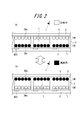
まず、本発明の情報表示用パネルのうち、帯電性粒子を含んだ粒子群を表示媒体として用いる情報表示用パネルの例を、図1および図2に基づき説明する。
図1に示す例では、少なくとも光学的反射率および帯電性を有する粒子を含んだ粒子群として構成した少なくとも2種類の表示媒体(ここでは負帯電性白色粒子3Waを含んだ粒子群として構成した白色表示媒体3Wと正帯電性黒色粒子3Baを含んだ粒子群として構成した黒色表示媒体3Bを示す)を、隔壁4で形成された各セル7において、背面側の基板1に設けた電極5(ストライプ電極)と観察側の透明な基板2に設けた透明電極6(ストライプ電極)とが対向交差(好ましくは対向直交交差)して形成する画素電極対の間に電圧を印加することにより発生する電界に応じて、基板1、2と垂直に移動させる。そして、図1(a)に示すように白色表示媒体3Wを観察者に視認させて白色の表示を、あるいは、図1(b)に示すように黒色表示媒体3Bを観察者に視認させて黒色の表示を、白黒のドットでマトリックス表示している。ここでは、セル7と画素(ドット)とが1対1に対応する例を示している。また、セル7内を空気で満たしているが、他の気体で満たしたり、真空としたりしてもよい。また、絶縁液体を満たしてもよい。
図2に示す例では、少なくとも光学的反射率および帯電性を有する粒子を含んだ粒子群として構成した少なくとも2種類の表示媒体(ここでは負帯電性白色粒子3Waを含んだ粒子群として構成した白色表示媒体3Wと正帯電性黒色粒子3Baを含んだ粒子群として構成した黒色表示媒体3Bを示す)を、隔壁4で形成された各セル7において、背面側の基板1に設けた電極5(TFT(薄膜トランジスタ)付き画素電極)と観察側の透明な基板2に設けた透明電極6(共通電極)との間に電圧を印加することにより発生する電界に応じて、基板1、2との間で垂直に移動させる。そして、図2(a)に示すように白色表示媒体3Wを観察者に視認させて白色の表示を、あるいは、図2(b)に示すように黒色表示媒体3Bを観察者に視認させて黒色の表示を、白黒のドットでマトリックス表示している。ここでは、セル7と画素(ドット)とが1対1に対応する例を示している。また、セル7内を空気で満たしているが、他の気体で満たしたり、真空としたりしてもよい。また、絶縁液体を満たしてもよい。
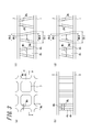
図3(a)は、本発明の情報表示用パネルの隔壁を説明するための平面図であり、図3(b)は、図3(a)のA-A断面図である。隔壁4は、四角形のセル7の辺を構成する辺部4hと、セル7の角を構成する交点部4kと、からなり、セル7は格子状に配置されている。平面図において、交点部4kは八角形であり、交点部4kの幅Wkは辺部4hの幅Whより広い。
辺部4hの幅Whは、通常のものより狭いため(0.1μm~10μmであることが好ましい)、情報表示用パネルの開口率を向上させることができる。ただし、辺部4hの幅Whを単に狭くすると、上述したように、情報表示用パネルの強度が不足するおそれがあるため、交点部4kの幅Wkを、辺部4hの幅Whより広くして、交点部4kにより情報表示用パネルの強度を確保している。なお、交点部4kの幅Wkは、11μm~50μmであることが好ましい。
辺部4hの幅Whは、通常のものより狭いため(0.1μm~10μmであることが好ましい)、情報表示用パネルの開口率を向上させることができる。ただし、辺部4hの幅Whを単に狭くすると、上述したように、情報表示用パネルの強度が不足するおそれがあるため、交点部4kの幅Wkを、辺部4hの幅Whより広くして、交点部4kにより情報表示用パネルの強度を確保している。なお、交点部4kの幅Wkは、11μm~50μmであることが好ましい。
図3(c)は、本発明の情報表示用パネルの隔壁の好適例を説明するための図である。辺部4hは、観察側の基板2から背面側の基板1に向かってテーパーが形成され、隔壁断面における、辺部4hの観察側の端部幅Wh2が、観察側とは反対側である背面側の端部幅Wh1より小さい。さらに、交点部4kも、観察側の基板2から背面側の基板1に向かってテーパーが形成され、隔壁断面における、交点部4kの観察側の端部幅Wk2が、背面側の端部幅Wk1より小さい。このように、辺部4hおよび交点部4kをテーパー状に形成することにより、開口率を向上させるとともに、情報表示用パネルの強度を確保することができる。なお、隔壁4をインプリント法により製造する場合、モールドから離型しやすいという利点も有している。
辺部4hおよび交点部4kのそれぞれのテーパー角θh、θkは、5°以上であることが好ましい。テーパー角θh、θkが5°未満の場合は、辺部4hおよび交点部4kが柱体の場合と大差ないためである。
なお、辺部4hおよび交点部4kにテーパーが形成されている場合は、断面図の同じ高さにおいて、交点部4kの幅Wkが辺部4hの幅Whより広いことが肝要である。
辺部4hおよび交点部4kのそれぞれのテーパー角θh、θkは、5°以上であることが好ましい。テーパー角θh、θkが5°未満の場合は、辺部4hおよび交点部4kが柱体の場合と大差ないためである。
なお、辺部4hおよび交点部4kにテーパーが形成されている場合は、断面図の同じ高さにおいて、交点部4kの幅Wkが辺部4hの幅Whより広いことが肝要である。
図3(d)は、本発明の情報表示用パネルの隔壁のその他の好適例を説明するための図である。辺部4hおよび交点部4kは、観察側の基板2から背面側の基板1に向かってテーパーが形成されており、さらに、辺部4hは、観察側の基板2から、表示媒体が通過しない程度の距離、離れている。すなわち、辺部4hの高さは、交点部4kの高さ(すなわち、基板1と基板2との間隔)より低い。表示媒体が通過しない程度の距離としては、表示媒体として帯電性粒子を用いる場合には、粒子径分布測定より得られる粒子径d(0.1)以下、好ましくは粒子径d(0)以下である。d(0.1)はこれ以下の粒子の比率が10%である粒子径をμmで表した数値、d(0)はこれ以下の粒子が0%である粒子径をμmで表した数値である。この場合、辺部4hは、情報表示用パネルの強度の向上に寄与しないが、交点部4kにより必要な強度を確保できればよい。辺部4hを観察側の基板2から離すことにより、辺部4hと基板2との間に接着剤を設ける必要がなくなり、製造が容易になるとともに、接着剤による反射率の低下がなくなる。さらには観察側から隔壁が確認できなくなり、より高精細な表示が可能になる。
また、図示は省略するが、辺部4hと交点部4kとが、表示媒体が通過しない程度の距離、離れていてもよい。
また、図示は省略するが、辺部4hと交点部4kとが、表示媒体が通過しない程度の距離、離れていてもよい。
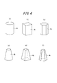
図4に、隔壁4の交点部4kの変形例を示す。交点部4kは、図3(a)に示した八角柱の他、図4(a)に示す円柱、図4(b)に示す四角柱、図4(c)に示す六角柱など、任意の柱体とすることができる。また、図4(d)に示す、円錐の頂点部分を取り除いたような、小円を上面、大円を下面とした形状、図4(e)に示す、四角錐の頂点部分を取り除いたような、小さい正方形を上面、大きい正方形を下面とした形状、図4(f)に示す、六角錐の頂点部分を取り除いたような、小さい正六角形を上面、大きい正六角形を下面とした形状にすることもできる。
上述した例では、四角形のセル7が格子状に配置されている場合を説明したが、セル7の形状は、四角形の他、三角形、円形、六角形なども可能であり、セル7の配置は、格子状やハニカム状や網目状なども可能である。これらのセル7の形状と配置を任意に組み合わせて、各種変形が可能である。
隔壁4の高さは、5μm~100μmの範囲とし、帯電性粒子を含んだ粒子群を表示媒体とする方式の情報表示用パネルでは、隔壁4の高さを、10μm~100μmの範囲とすることが好ましい。
隔壁4の高さは、5μm~100μmの範囲とし、帯電性粒子を含んだ粒子群を表示媒体とする方式の情報表示用パネルでは、隔壁4の高さを、10μm~100μmの範囲とすることが好ましい。
以下、隔壁の形成方法および隔壁材料について説明する。
隔壁の形成方法としては、インプリント法、スクリーン印刷法、凸版印刷法、凹版印刷法、サンドブラスト法、フォトリソ法等がある。そのうち、インプリント法は、フォトリソ法に比べて工程数が少なく加工時間の短縮が可能であり、廃液の発生もなく環境的にも優れた方法であるので好ましい。特に、紫外線硬化性組成物を紫外線により硬化させるUVインプリント法を用いると、隔壁の形成工程が室温で実施可能となり、熱収縮等の影響による寸法ズレを抑制できるので好ましい。
隔壁の形成方法としては、インプリント法、スクリーン印刷法、凸版印刷法、凹版印刷法、サンドブラスト法、フォトリソ法等がある。そのうち、インプリント法は、フォトリソ法に比べて工程数が少なく加工時間の短縮が可能であり、廃液の発生もなく環境的にも優れた方法であるので好ましい。特に、紫外線硬化性組成物を紫外線により硬化させるUVインプリント法を用いると、隔壁の形成工程が室温で実施可能となり、熱収縮等の影響による寸法ズレを抑制できるので好ましい。
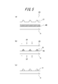
図5を用いて、UVインプリント法による隔壁の形成方法を説明する。
図5(a)に示すように、背面側の基板1の上に、紫外線硬化性樹脂組成物である隔壁材料40を塗布する。次に、隔壁のパターンに対応した凹部21を有するモールド20を、隔壁材料40が塗布された基板1上に載置、押圧する。すると、図5(b)に示すように、モールド20の凹部21内に未硬化状態の隔壁材料40が充填される。次に、モールド20または基板1のうち、透明な部材側から紫外線を照射し、未硬化状態の隔壁材料40を硬化させる。その後、図5(c)に示すように、モールド20から基板1を離型することで、基板1の基板面に所望のパターンの隔壁4が形成される。
図5(a)に示すように、背面側の基板1の上に、紫外線硬化性樹脂組成物である隔壁材料40を塗布する。次に、隔壁のパターンに対応した凹部21を有するモールド20を、隔壁材料40が塗布された基板1上に載置、押圧する。すると、図5(b)に示すように、モールド20の凹部21内に未硬化状態の隔壁材料40が充填される。次に、モールド20または基板1のうち、透明な部材側から紫外線を照射し、未硬化状態の隔壁材料40を硬化させる。その後、図5(c)に示すように、モールド20から基板1を離型することで、基板1の基板面に所望のパターンの隔壁4が形成される。
ここで、隔壁材料40としての紫外線硬化性樹脂組成物はどのようなものを用いてもよいが、特にインプリント法に使用できる液状の紫外線硬化性樹脂組成物が好ましい。液状の紫外線硬化性樹脂組成物は一般に、粘度は0.1Pa・s~100Pa・sが好ましい。
紫外線硬化性樹脂組成物は紫外線硬化性樹脂と光開始剤を含む組成物が好ましい。
紫外線硬化性樹脂としては、例えば、ウレタンアクリレート、ポリエステルアクリレート、エポキシアクリレート、エポキシ樹脂、イミド系オリゴマー、ポリエン・チオール系オリゴマー等が挙げられる。
紫外線硬化性樹脂としては、例えば、ウレタンアクリレート、ポリエステルアクリレート、エポキシアクリレート、エポキシ樹脂、イミド系オリゴマー、ポリエン・チオール系オリゴマー等が挙げられる。
ウレタンアクリレートは、例えば、ヘキサメチレンジイソシアネート、イソホロンジイソシアネート、メチレンビス(4-シクロヘキシルイソシアネート)、トリメチルヘキサメチレンジイソシアネート、トリレンジイソシアネート、4,4-ジフェニルメタンジイソシアネート、キシリレンジイソシアネート等のジイソシアネート類とポリ(プロピレンオキサイド)ジオール、ポリ(プロピレンオキサイド)トリオール、ポリ(テトラメチレンオキサイド)ジオール、エトキシ化ビスフェノールA等のポリオール類と2-ヒドロキシエチルアクリレート2-ヒドロキシエチルメタクリレート、2-ヒドロキシプロピルアクリレート、グリシドールジメタクリレート、ペンタエリスリトールトリアクリレート等のヒドロキシアクリレート類を反応させることによって得られ、分子中に官能基としてアクリロイル基とウレタン結合を有するものである。
ポリエステルアクリレートとしては、例えば、無水フタル酸とプロピレンオキサイドとアクリル酸とからなるポリエステルアクリレート、アジピン酸と1,6-ヘキサンジオールとアクリル酸とからなるポリエステルアクリレート、トリメリット酸とジエチレングリコールとアクリル酸とからなるポリエステルアクリレート等が挙げられる。
エポキシアクリレートは、エピクロルヒドリン等のエポキシ化合物とアクリル酸又はメタクリル酸との反応により合成されたものであり、例えば、ビスフェノールAとエピクロルヒドリンとアクリル酸との反応により合成されるビスフェノールA型エポキシアクリレート、ビスフェノールSとエピクロルヒドリンとアクリル酸との反応により合成されるビスフェノールS型エポキシアクリレート、ビスフェノールFとエピクロルヒドリンとアクリル酸との反応により合成されるビスフェノールF型エポキシアクリレート、フェノールノボラックとエピクロルヒドリンとアクリル酸との反応により合成されるフェノールノボラック型エポキシアクリレート等が挙げられる。
エポキシ樹脂としては、例えば、ビスフェノールA型エポキシ樹脂、ビスフェノールF型エポキシ樹脂、ビスフェノールAD型エポキシ樹脂、ビスフェノールS型エポキシ樹脂等のビスフェノール型エポキシ樹脂;フェノールノボラック型エポキシ樹脂、クレゾールノボラック型エポキシ樹脂等のノボラック型エポキシ樹脂;トリスフェノールメタントリグリシジルエーテル等の芳香族エポキシ樹脂、および、これらの水添化物や臭素化物等が挙げられる。
光重合開始剤としては、光ラジカル重合開始剤および光カチオン重合開始剤が好ましく、光ラジカル重合開始剤としては、例えば、4-(2-ヒドロキシエトキシ)フェニル(2-ヒドロキシ-2-プロピル)ケトン、α-ヒドロキシ-α-α’-ジメチルアセトフェノン、メトキシアセトフェノン、2,2-ジメトキシ-2-フェニルアセトフェノン等のアセトフェノン誘導体;ベンゾインエチルエーテル、ベンゾインプロピルエーテル等のベンゾインエーテル系化合物;ベンジルジメチルケタール等のケタール誘導体;ハロゲン化ケトン、アシルフォスフィンオキシド、アシルフォスフォナート、2-メチル-1-[4-(メチルチオ)フェニル]-2-モルフォリノプロパン-1-オン、2-ベンジル-2-N,N-ジメチルアミノ-1-(4-モルフォリノフェニル)-1-ブタン、ビス(2,4,6-トリメチルベンゾイル)-フェニルフォスフィンオキシドビス-(2,6-ジメトキシベンゾイル)2,4,4-トリメチルペンチルフォスフィンオキシド、ビス(η5-シクロペンタジエニル)-ビス(ペンタフルオロフェニル)-チタニウム、ビス(η5-シクロペンタジエニル)-ビス[2,6-ジフルオロー3-(1H-ピリ-1-イル)フェニル]-チタニウム、アントラセン、ペリレン、コロネン、テトラセン、ベンズアントラセン、フェノチアジン、フラビン、アクリジン、ケトクマリン、チオキサントン誘導体、ベンゾフェノン、アセトフェノン、2-クロロチオキサンソン、2,4-ジメチルチオキサンソン、2,4-ジエチルチオキサンソン、2,4-ジイソプロピルチオキサンソン、イソプロピルチオキサンソン等が挙げられる。光カチオン重合開始剤としては、例えば、鉄-アレン錯体化合物、芳香族ジアゾニウム塩、芳香族ヨードニウム塩、芳香族スルホニウム塩、オニウム塩、ピリジニウム塩、アルミニウム錯体/シラノール塩、トリクロロメチルトリアジン誘導体等が挙げられる。上記オニウム塩やピリジニウム塩の対アニオンとしては、例えば、SbF6-、PF6-、AsF6-、BF4-、テトラキス(ペンタフルオロ)ボレート、トリフルオロメタンスルフォネート、メタンスルフォネート、トリフルオロアセテート、アセテート、スルフォネート、トシレート、ナイトレート等が挙げられる。
光重合開始剤の添加量は、一般に紫外線硬化性樹脂100質量部に対して、0.1~15質量部であり、好ましくは、0.5~10質量部である。
光重合開始剤の添加量は、一般に紫外線硬化性樹脂100質量部に対して、0.1~15質量部であり、好ましくは、0.5~10質量部である。
紫外線硬化性樹脂組成物には、反応性希釈剤が添加されてもよく、反応性希釈剤としては、例えば、1,4-ブタンジオールジアクリレート、1,6-ヘキサンジオールジアクリレート、ネオペンチルグリコールジアクリレート、2-(2-エトキシエトキシ)エチルアクリレート、テトラヒドロフルフリルアクリレート、2-フェノキシエチルアクリレート、ジエチレングリコールジアクリレート、テトラエチレングリコールジアクリレート、1,3-ブチレングリコールジアクリレート、トリプロピレングリコールジアクリレート、トリメチロールプロパントリアクリレート、ペンタエリスリトールテトラアクリレート、ヒドロキシピバリン酸ネオペンチルグリコールジアクリレート等が挙げられる。
紫外線硬化性樹脂組成物には、更に、必要に応じて、一般に添加されている光重合開始助剤、熱重合禁止剤、充填剤、接着付与剤、チクソ付与剤、可塑剤、着色剤等が添加されていてもよい。
紫外線硬化性樹脂組成物には、更に、必要に応じて、一般に添加されている光重合開始助剤、熱重合禁止剤、充填剤、接着付与剤、チクソ付与剤、可塑剤、着色剤等が添加されていてもよい。
以下、情報表示用パネルの各部材について説明する。
情報表示用パネルの基板1、2は、少なくとも観察側の基板2の表示領域が、情報表示用パネルの外側から表示媒体の色が確認できる透明な基板であり、可視光の透過率が高く且つ耐熱性の良い材料から成る基板であることが好ましい。背面側の基板1は、透明でも不透明でも構わないが、UVインプリント法により隔壁を製造する場合、不透明なモールドを用いる際は、UV光を背面側の基板1の側から紫外線を照射するため、透明であることが好ましい。
情報表示用パネルの基板1、2は、少なくとも観察側の基板2の表示領域が、情報表示用パネルの外側から表示媒体の色が確認できる透明な基板であり、可視光の透過率が高く且つ耐熱性の良い材料から成る基板であることが好ましい。背面側の基板1は、透明でも不透明でも構わないが、UVインプリント法により隔壁を製造する場合、不透明なモールドを用いる際は、UV光を背面側の基板1の側から紫外線を照射するため、透明であることが好ましい。
また基板1、2としては、例えば、ポリエチレンテレフタレート(PET)、ポリエチレンナフタレート(PEN)、ポリエーテルサルフォン(PES)、ポリエチレン(PE)、ポリカーボネート(PC)、ポリイミド(PI)、アクリルなどの樹脂基板や、絶縁被覆された金属基板、ガラス基板等を用いることができる。基板材料は何でもよく、刃やレーザー加工、超音波加工によって切断できるものであればよい。切断を容易にするために基板1、2の厚さは薄い方が良いが、薄すぎると製造工程でのハンドリング性が悪化するため、基板1、2の厚さは、好ましくは25μm~1000μmの範囲であり、さらに好ましくは25μm~800μmの範囲である。
電極の形成材料としては、アルミニウム、銀、ニッケル、銅、金等の金属類や酸化インジウム錫(ITO)、酸化インジウム亜鉛(IZO)、アルミニウムドープ酸化亜鉛(AZO)、酸化インジウム、導電性酸化錫、アンチモン錫酸化物(ATO)、導性酸化亜鉛等の導電金属酸化物類、ポリアニリン、ポリピロール、PEDOT/PSS等を含むポリチオフェンなどの導電性高分子類が例示され、適宜選択して用いられる。電極の形成方法としては、上記例示の材料をスパッタリング法、真空蒸着法、CVD(化学蒸着)法、塗布法等で薄膜状にパターニング形成する方法、金属箔(例えば圧延銅箔など)をラミネートする方法や、導電剤を溶媒や合成樹脂バインダーに混合して塗布してパターニング形成する方法が用いられる。観察側の基板2の表示領域に設ける電極は透明である必要があるが、背面側の基板1や表示領域外に設ける電極は透明である必要がない。ただし、上述したUVインプリント法により隔壁を製造する場合、不透明なモールドを使用する際は、UV光を背面側の基板1の側から紫外線を照射するため、透明であることが好ましい。いずれの場合もパターン形成可能である導電性である上記材料を好適に用いることができる。なお、電極の厚みは、導電性や光透過性を鑑みて決定され、0.01μm~10μm、好ましくは0.05μm~5μmである。
情報表示用パネルの表示媒体として帯電性粒子を用いる場合には、帯電性粒子(以下、粒子ともいう)は平均粒子径d(0.5)が、1μm~20μmの範囲であり、均一で揃っていることが好ましい。平均粒子径d(0.5)がこの範囲より大きいと表示上の鮮明さに欠け、この範囲より小さいと粒子同士の凝集力が大きくなりすぎるために表示媒体としての移動に支障をきたすようになる。
さらに、粒子径分布に関して、下記式に示される粒子径分布Spanを5未満、好ましくは3未満とする。
Span=(d(0.9)-d(0.1))/d(0.5)
(但し、d(0.5)は粒子の50%がこれより大きく、50%がこれより小さいという粒子径をμmで表した数値、d(0.1)はこれ以下の粒子の比率が10%である粒子径をμmで表した数値、d(0.9)はこれ以下の粒子が90%である粒子径をμmで表した数値である。)
Spanを5以下の範囲に納めることにより、帯電性粒子のサイズが揃い、均一な表示媒体としての移動が可能となる。
Span=(d(0.9)-d(0.1))/d(0.5)
(但し、d(0.5)は粒子の50%がこれより大きく、50%がこれより小さいという粒子径をμmで表した数値、d(0.1)はこれ以下の粒子の比率が10%である粒子径をμmで表した数値、d(0.9)はこれ以下の粒子が90%である粒子径をμmで表した数値である。)
Spanを5以下の範囲に納めることにより、帯電性粒子のサイズが揃い、均一な表示媒体としての移動が可能となる。
さらにまた、帯電極性の異なる2種類の帯電性粒子を表示媒体として使用する本発明の場合には、平均粒子径d(0.5)が大きい帯電性粒子の平均粒子径d(0.5)に対する、平均粒子径d(0.5)が小さい帯電性粒子の平均粒子径d(0.5)の比を10以下とすることが肝要である。たとえ粒子径分布Spanを小さくしたとしても、互いに帯電極性の異なる帯電性粒子が動くので、互いの粒子サイズを同程度にすることで表示媒体として容易に移動できるようになるので好適であり、それがこの範囲となる。
なお、上記の粒子径分布および粒子径は、レーザー回折/散乱法などから求めることができる。測定対象となる粒子にレーザー光を照射すると空間的に回折/散乱光の光強度分布パターンが生じ、この光強度パターンは粒子径と対応関係があることから、粒子径および粒子径分布が測定できる。
ここで、粒子径および粒子径分布は、体積基準分布から得られたものである。具体的には、Mastersizer2000(Malvern Instruments Ltd.)測定機を用いて、窒素気流中に粒子を投入し、付属の解析ソフト(Mie理論を用いた体積基準分布を基本としたソフト)にて、粒子径および粒子径分布の測定を行なうことができる。
ここで、粒子径および粒子径分布は、体積基準分布から得られたものである。具体的には、Mastersizer2000(Malvern Instruments Ltd.)測定機を用いて、窒素気流中に粒子を投入し、付属の解析ソフト(Mie理論を用いた体積基準分布を基本としたソフト)にて、粒子径および粒子径分布の測定を行なうことができる。
さらに、帯電性粒子を含んだ粒子群として構成する表示媒体を気体中(真空中を含む)空間で駆動させる方式とする場合には、基板間の表示媒体を取り巻く空隙部分の気体の管理が重要であり、表示安定性向上に寄与する。具体的には、空隙部分の気体の湿度について、25℃における相対湿度を60%RH以下、好ましくは50%RH以下とすることが重要である。
この空隙部分とは、図1および図2において、対向する基板1、2に挟まれる部分から、電極5、6(電極を基板の内側に設けた場合)、表示媒体3の占有部分、隔壁4の占有部分、パネルのシール部分を除いた、いわゆる表示媒体が接する気体部分を指すものとする。
空隙部分の気体は、先に述べた湿度領域であれば、その種類は問わないが、乾燥空気、乾燥窒素、乾燥アルゴン、乾燥ヘリウム、乾燥二酸化炭素、乾燥メタンなどが好適である。この気体は、その湿度が保持されるようにパネルに封入することが必要であり、例えば、表示媒体の充填、パネルの組み立てなどを所定湿度環境下にて行い、さらに、外からの湿度侵入を防ぐシール材、シール方法を施すことが肝要である。
また、基板間の気体中(真空中を含む)空間における表示媒体の体積占有率は5%~70%が好ましく、さらに好ましくは5%~60%である。70%を超える場合には表示媒体としての粒子の移動に支障をきたし、5%未満の場合にはコントラストが不明確となり易い。
帯電性粒子を移動させて表示する方式には、この帯電性粒子を絶縁液体とともにセルに封止したものもあるが、本発明は、このような方式の情報表示用パネルにも適用できる。
帯電性粒子を移動させて表示する方式には、この帯電性粒子を絶縁液体とともにセルに封止したものもあるが、本発明は、このような方式の情報表示用パネルにも適用できる。
以下、本発明の実施例について説明するが、本発明はこれだけに限定されるものではない。
以下の工程(1)~(5)によって、発明例および比較例の情報表示用パネルを製作した。製作した各情報表示用パネルの隔壁の仕様を表1に示す。
(1)ITO電極パターンが形成された厚さ0.7mmのガラス基板へ、UVインプリント法により隔壁を形成する。
(2)隔壁を形成したガラス基板へ、表示媒体(d(0)=6μm)を充填する。
(3)隔壁上の不要な表示媒体を除去する。
(4)隔壁上に接着剤層を形成する。接着剤の硬化温度は110℃である。
(5)2枚の基板を、110℃、1時間で熱プレスすることにより貼り合わせる。
以下の工程(1)~(5)によって、発明例および比較例の情報表示用パネルを製作した。製作した各情報表示用パネルの隔壁の仕様を表1に示す。
(1)ITO電極パターンが形成された厚さ0.7mmのガラス基板へ、UVインプリント法により隔壁を形成する。
(2)隔壁を形成したガラス基板へ、表示媒体(d(0)=6μm)を充填する。
(3)隔壁上の不要な表示媒体を除去する。
(4)隔壁上に接着剤層を形成する。接着剤の硬化温度は110℃である。
(5)2枚の基板を、110℃、1時間で熱プレスすることにより貼り合わせる。
工程(1)~(5)によって得られた発明例および比較例の情報表示用パネルについて、隔壁よれ、表示品位および荷重解放後の表示品位変化を観察し、結果をあわせて表1に示す。
「隔壁よれ」は顕微鏡により隔壁状態(隔壁のよれの有無)を観察することで評価した。
「表示品位」は、評価パネルの電極間に80Vの電圧を電圧の向きを変えて印加することで、評価パネルにおいて白表示および黒表示を行い、白表示および黒表示のそれぞれにおいて、光学濃度計(サカタインクスエンジニアリング(株):RD19I)を用いてOD値(光学濃度)の測定を行った。白表示のOD(WOD)と黒表示のOD(BOD)をもとにコントラストCR=10(BOD-WOD)を算出し、これをパネル性能の指標とした。80V駆動時のコントラストCRがCR>8となる場合を◎とし、6<CR≦8となる場合を○、4<CR≦6となる場合を△、CR≦4となる場合を×とした。
「荷重解放後の表示品位変化」は、分銅(Φ53mm、重さ1kg)を各情報表示用パネル上に載せ、1時間放置後、分銅を取り除いた後の表示品位を測定し、荷重を加える前の表示品位(CR前)と、荷重解放後の表示品位(CR後)の割合(CR後/CR前×100)が80%以上であれば○、80%未満は×とした。

発明例1、2、3は隔壁よれが発生せず、表示品位は良好であった。また、荷重解放後の表示品位変化も小さく良好であった。特に、発明例3はあたかも隔壁が存在しないように観察され、画面全体が最も明るく、非常に良好であった。
比較例1、2は隔壁よれが発生し、表示品位は不良であった。また、荷重解放の表示品位変化は大きかった。
比較例3は隔壁よれが発生しなかった。また、表示品位は比較的良好であったが、観察側の隔壁幅が大きいため画面全体が暗かった。また、荷重解放後の表示品位変化は無く良好であった。
比較例1、2は隔壁よれが発生し、表示品位は不良であった。また、荷重解放の表示品位変化は大きかった。
比較例3は隔壁よれが発生しなかった。また、表示品位は比較的良好であったが、観察側の隔壁幅が大きいため画面全体が暗かった。また、荷重解放後の表示品位変化は無く良好であった。
1 基板
2 基板
3W 白色表示媒体
3Wa 白色粒子
3B 黒色表示媒体
3Ba 黒色粒子
4 隔壁
4h 辺部
4k 交点部
5 電極
6 電極
20 モールド
21 凹部
40 隔壁材料
2 基板
3W 白色表示媒体
3Wa 白色粒子
3B 黒色表示媒体
3Ba 黒色粒子
4 隔壁
4h 辺部
4k 交点部
5 電極
6 電極
20 モールド
21 凹部
40 隔壁材料
Claims (4)
- 互いに対向する2枚の基板間に形成された隔壁で区画されたセル内に、帯電性を有する少なくとも2種類の表示媒体を封入し、前記表示媒体に、前記2枚の基板に設けた電極から電界を付与することにより前記表示媒体を前記2枚の基板間で移動させて画像等の情報を表示する情報表示用パネルにおいて、
前記隔壁は、前記セルの辺を構成する辺部と、前記セルの角を構成する交点部と、からなり、前記交点部は、前記辺部より幅が広い、
ことを特徴とする情報表示用パネル。 - 前記辺部は、観察側の基板から背面側の基板に向かってテーパーが形成され、
隔壁断面における、前記辺部の観察側の端部幅が、観察側とは反対側の端部幅より小さい、
ことを特徴とする請求項1に記載の情報表示用パネル。 - 前記交点部は、観察側の基板から背面側の基板に向かってテーパーが形成され、
隔壁断面における、前記交点部の観察側の端部幅が、観察側とは反対側の端部幅より小さい、
ことを特徴とする請求項1または2に記載の情報表示用パネル。 - 前記辺部が、観察側の基板から離れて形成され、
前記辺部の高さが、前記交点部の高さより低い、
ことを特徴とする請求項1~3のいずれかに記載の情報表示用パネル。
Applications Claiming Priority (2)
| Application Number | Priority Date | Filing Date | Title |
|---|---|---|---|
| JP2011-055680 | 2011-03-14 | ||
| JP2011055680A JP2012189963A (ja) | 2011-03-14 | 2011-03-14 | 情報表示用パネル |
Publications (1)
| Publication Number | Publication Date |
|---|---|
| WO2012124325A1 true WO2012124325A1 (ja) | 2012-09-20 |
Family
ID=46830411
Family Applications (1)
| Application Number | Title | Priority Date | Filing Date |
|---|---|---|---|
| PCT/JP2012/001785 Ceased WO2012124325A1 (ja) | 2011-03-14 | 2012-03-14 | 情報表示用パネル |
Country Status (2)
| Country | Link |
|---|---|
| JP (1) | JP2012189963A (ja) |
| WO (1) | WO2012124325A1 (ja) |
Cited By (1)
| Publication number | Priority date | Publication date | Assignee | Title |
|---|---|---|---|---|
| EP4692918A4 (en) * | 2024-04-15 | 2026-05-06 | Wuxi Vision Peak Technology Co Ltd | THIN-FILM TRANSISTOR PLASMA DISPLAY MODULE WITH AN INSULATING STRUCTURE AND A PLASMA DISPLAY SCREEN |
Citations (3)
| Publication number | Priority date | Publication date | Assignee | Title |
|---|---|---|---|---|
| JP2002196376A (ja) * | 2000-12-27 | 2002-07-12 | Fuji Xerox Co Ltd | 画像表示媒体 |
| JP2008051932A (ja) * | 2006-08-23 | 2008-03-06 | Brother Ind Ltd | 電気泳動表示媒体 |
| JP2009251215A (ja) * | 2008-04-04 | 2009-10-29 | Dainippon Printing Co Ltd | 電気泳動表示装置 |
-
2011
- 2011-03-14 JP JP2011055680A patent/JP2012189963A/ja not_active Withdrawn
-
2012
- 2012-03-14 WO PCT/JP2012/001785 patent/WO2012124325A1/ja not_active Ceased
Patent Citations (3)
| Publication number | Priority date | Publication date | Assignee | Title |
|---|---|---|---|---|
| JP2002196376A (ja) * | 2000-12-27 | 2002-07-12 | Fuji Xerox Co Ltd | 画像表示媒体 |
| JP2008051932A (ja) * | 2006-08-23 | 2008-03-06 | Brother Ind Ltd | 電気泳動表示媒体 |
| JP2009251215A (ja) * | 2008-04-04 | 2009-10-29 | Dainippon Printing Co Ltd | 電気泳動表示装置 |
Cited By (1)
| Publication number | Priority date | Publication date | Assignee | Title |
|---|---|---|---|---|
| EP4692918A4 (en) * | 2024-04-15 | 2026-05-06 | Wuxi Vision Peak Technology Co Ltd | THIN-FILM TRANSISTOR PLASMA DISPLAY MODULE WITH AN INSULATING STRUCTURE AND A PLASMA DISPLAY SCREEN |
Also Published As
| Publication number | Publication date |
|---|---|
| JP2012189963A (ja) | 2012-10-04 |
Similar Documents
| Publication | Publication Date | Title |
|---|---|---|
| JP4224227B2 (ja) | 帯電防止性ハードコートフィルム及びその製造方法 | |
| JP4929578B2 (ja) | 液晶表示装置 | |
| JP4276988B2 (ja) | 液晶表示装置およびその製造方法 | |
| JPWO2011027909A1 (ja) | 導電性光学素子、タッチパネル、情報入力装置、表示装置、太陽電池、および導電性光学素子作製用原盤 | |
| TWI411632B (zh) | 環保光學片 | |
| KR20060121812A (ko) | 가요성 몰드, 그의 제조 방법 및 미세 구조체의 제조 방법 | |
| JP2011034060A (ja) | 光学シートの製造方法、光学シート、及び映像表示装置 | |
| WO2004010452A2 (en) | Flexible mold and method of manufacturing microstructure using same | |
| JPWO2004001498A1 (ja) | 画像表示装置及び画像表示装置の製造方法 | |
| JP4488674B2 (ja) | 光硬化性樹脂組成物、液晶パネル用基板、及び、液晶パネル | |
| CN102227475A (zh) | 具有遮光性与粘合性的光固化性树脂组合物及其固化物 | |
| JP4657923B2 (ja) | 画像表示用パネルの製造方法 | |
| JP4533611B2 (ja) | 液晶表示装置 | |
| JP2012189963A (ja) | 情報表示用パネル | |
| JP5490487B2 (ja) | 光学積層体 | |
| JP5753285B2 (ja) | 光学積層体 | |
| JP2012189962A (ja) | 情報表示用パネル | |
| JP2012078547A (ja) | 情報表示用パネルの製造方法及び情報表示用パネル | |
| JP2012018254A (ja) | 情報表示用パネルの製造方法 | |
| JP2012002963A (ja) | 情報表示用パネルの製造方法 | |
| JP2012093469A (ja) | 情報表示用パネルの製造方法及び情報表示用パネル | |
| JP7646758B2 (ja) | 光学デバイス、光学デバイスの製造方法及び電子機器 | |
| JP2011107335A (ja) | 光学積層体 | |
| JP2013156313A (ja) | 情報表示用パネルの製造方法 | |
| CN104155706A (zh) | 紫外线树脂、凹透镜、可切换透镜、立体显示器及其制作方法 |
Legal Events
| Date | Code | Title | Description |
|---|---|---|---|
| 121 | Ep: the epo has been informed by wipo that ep was designated in this application |
Ref document number: 12758095 Country of ref document: EP Kind code of ref document: A1 |
|
| NENP | Non-entry into the national phase |
Ref country code: DE |
|
| 122 | Ep: pct application non-entry in european phase |
Ref document number: 12758095 Country of ref document: EP Kind code of ref document: A1 |